EP0786737A2 - Non-contact type IC card - Google Patents
Non-contact type IC card Download PDFInfo
- Publication number
- EP0786737A2 EP0786737A2 EP97105219A EP97105219A EP0786737A2 EP 0786737 A2 EP0786737 A2 EP 0786737A2 EP 97105219 A EP97105219 A EP 97105219A EP 97105219 A EP97105219 A EP 97105219A EP 0786737 A2 EP0786737 A2 EP 0786737A2
- Authority
- EP
- European Patent Office
- Prior art keywords
- data
- card
- area
- areas
- memory
- Prior art date
- Legal status (The legal status is an assumption and is not a legal conclusion. Google has not performed a legal analysis and makes no representation as to the accuracy of the status listed.)
- Granted
Links
- 230000005764 inhibitory process Effects 0.000 abstract description 23
- 230000002401 inhibitory effect Effects 0.000 abstract description 6
- 230000005856 abnormality Effects 0.000 description 8
- 239000003990 capacitor Substances 0.000 description 8
- 238000004891 communication Methods 0.000 description 6
- 238000010586 diagram Methods 0.000 description 6
- 230000006870 function Effects 0.000 description 6
- 230000008878 coupling Effects 0.000 description 5
- 238000010168 coupling process Methods 0.000 description 5
- 238000005859 coupling reaction Methods 0.000 description 5
- 238000013459 approach Methods 0.000 description 2
- 230000003247 decreasing effect Effects 0.000 description 2
- 238000009499 grossing Methods 0.000 description 2
- 102000004129 N-Type Calcium Channels Human genes 0.000 description 1
- 108090000699 N-Type Calcium Channels Proteins 0.000 description 1
- 238000010276 construction Methods 0.000 description 1
- 238000007599 discharging Methods 0.000 description 1
- 230000005672 electromagnetic field Effects 0.000 description 1
- 230000003628 erosive effect Effects 0.000 description 1
- 230000005669 field effect Effects 0.000 description 1
- 230000002829 reductive effect Effects 0.000 description 1
Images


Classifications
-
- G—PHYSICS
- G07—CHECKING-DEVICES
- G07F—COIN-FREED OR LIKE APPARATUS
- G07F7/00—Mechanisms actuated by objects other than coins to free or to actuate vending, hiring, coin or paper currency dispensing or refunding apparatus
- G07F7/08—Mechanisms actuated by objects other than coins to free or to actuate vending, hiring, coin or paper currency dispensing or refunding apparatus by coded identity card or credit card or other personal identification means
- G07F7/10—Mechanisms actuated by objects other than coins to free or to actuate vending, hiring, coin or paper currency dispensing or refunding apparatus by coded identity card or credit card or other personal identification means together with a coded signal, e.g. in the form of personal identification information, like personal identification number [PIN] or biometric data
- G07F7/1008—Active credit-cards provided with means to personalise their use, e.g. with PIN-introduction/comparison system
-
- G—PHYSICS
- G06—COMPUTING; CALCULATING OR COUNTING
- G06K—GRAPHICAL DATA READING; PRESENTATION OF DATA; RECORD CARRIERS; HANDLING RECORD CARRIERS
- G06K19/00—Record carriers for use with machines and with at least a part designed to carry digital markings
- G06K19/06—Record carriers for use with machines and with at least a part designed to carry digital markings characterised by the kind of the digital marking, e.g. shape, nature, code
- G06K19/067—Record carriers with conductive marks, printed circuits or semiconductor circuit elements, e.g. credit or identity cards also with resonating or responding marks without active components
- G06K19/07—Record carriers with conductive marks, printed circuits or semiconductor circuit elements, e.g. credit or identity cards also with resonating or responding marks without active components with integrated circuit chips
- G06K19/0723—Record carriers with conductive marks, printed circuits or semiconductor circuit elements, e.g. credit or identity cards also with resonating or responding marks without active components with integrated circuit chips the record carrier comprising an arrangement for non-contact communication, e.g. wireless communication circuits on transponder cards, non-contact smart cards or RFIDs
-
- G—PHYSICS
- G06—COMPUTING; CALCULATING OR COUNTING
- G06Q—INFORMATION AND COMMUNICATION TECHNOLOGY [ICT] SPECIALLY ADAPTED FOR ADMINISTRATIVE, COMMERCIAL, FINANCIAL, MANAGERIAL OR SUPERVISORY PURPOSES; SYSTEMS OR METHODS SPECIALLY ADAPTED FOR ADMINISTRATIVE, COMMERCIAL, FINANCIAL, MANAGERIAL OR SUPERVISORY PURPOSES, NOT OTHERWISE PROVIDED FOR
- G06Q20/00—Payment architectures, schemes or protocols
- G06Q20/30—Payment architectures, schemes or protocols characterised by the use of specific devices or networks
- G06Q20/34—Payment architectures, schemes or protocols characterised by the use of specific devices or networks using cards, e.g. integrated circuit [IC] cards or magnetic cards
- G06Q20/341—Active cards, i.e. cards including their own processing means, e.g. including an IC or chip
-
- G—PHYSICS
- G07—CHECKING-DEVICES
- G07F—COIN-FREED OR LIKE APPARATUS
- G07F7/00—Mechanisms actuated by objects other than coins to free or to actuate vending, hiring, coin or paper currency dispensing or refunding apparatus
- G07F7/08—Mechanisms actuated by objects other than coins to free or to actuate vending, hiring, coin or paper currency dispensing or refunding apparatus by coded identity card or credit card or other personal identification means
- G07F7/0806—Details of the card
- G07F7/0813—Specific details related to card security
- G07F7/082—Features insuring the integrity of the data on or in the card
Definitions
- the present invention relates to a non-contact type integrated circuit (IC) card not having contact terminals for a power source and for inputting and outputting signals.
- IC integrated circuit
- the card bearer having the card with him or her need only approach the reader and there is unnecessitated a read operation to insert the card into the reader. Consequently, the card is suitable for a check of sequential passage of many persons, for example, the card is suitably used as a commuter pass or a key for checking entrance an exit for a particular room.
- ID data is read from a memory of the IC card for a collation thereof such that when the collation results in a coincidence, the passage of the gate or the entrance for the room is admitted.
- historical data of uses of the IC card is written in the memory thereof.
- the collation and the write operation of the history are accomplished. Since the accessible area has a range of a certain magnitude, when the card is employed as, for example, a commuter pass, there may occur depending on actions of the card holder a case where an identical card enters two or more times the area accessible to the reader-writer installed at the gate. Namely, it may possible occur, the user puts the card into the area, removes the card from the area, and then puts again the card into the area. In such a case, it is necessary to avoid the write operation of history in the second access.
- the second access of an identical card is detected by the reader-writer to inhibit the write operation of new data on the card.
- the reader-writer since passage of many cards is required to be checked in a short period of time at the gate, it is necessary for the reader-writer, after an access of a card, to wait for passage of a subsequent card. Consequently, there does not exit any marginal time enough to check the second access.
- a card not having a power source therein namely, a card of an external power supply type
- an electromagnetic energy supplied from an external device is rectified to obtain a direct-current (dc) voltage necessary for an internal circuit thereof.
- dc direct-current
- the circuit in the card may be operated by energy resultant from discharge of electric charges accumulated in a smoothing capacitor of the power source circuit.
- the operation of the circuit is determined by a value of a current consumed by the circuit and the energy accumulated in the smoothing capacitor, it is difficult to set the period for inhibiting the operation.
- the present invention aims at providing a non-contact type IC card capable of preventing inappropriate data from being written therein even when the card enters an area accessible to the external device for a plurality of times at a short interval of time.
- another object of the present invention is to provide a non-contact type IC card guaranteeing the normal operation even when an abnormality occurs in the contact state during a write operation of data from the external device.
- a non-contact type IC card achieving communications of signals with an external device in a noncontact manner includes main circuit means for conducting various operations based on functions of the IC card, operation inhibition signal generating means for creating an operation inhibition signal to inhibit the operation of the main circuit means for a predetermined period of time, and control means for controlling the main circuit means and the operation inhibition signal generating means.
- the control means operates the operation inhibition signal generating means when the operation of the main circuit means is finished and inhibits the operation of the main circuit means for a predetermined period of time according to the operation inhibition signal from the operation inhibition signal generating means.
- the operation inhibition signal generating means operates to create an operation inhibition signal, thereby inhibiting the operation of the main circuit means for a predetermined period of time.
- the second and subsequent accesses can be inhibited and hence the improper operation due to the plural accesses can be avoided.
- the inhibition of such accesses need not be monitored by the external device, the load imposed on the external device can be minimized.
- a non-contact type IC card includes communicating means for communicating signals with an external device in a noncontact manner, a memory for storing therein data sent from the external device, and control means for controlling operations of the communicating means and the memory.
- the memory has an area subdivided into a plurality of areas for storing therein data sent from the external device, and the control means reads, when the data is to be read from the memory, the data from one of the plural areas in which the data is normally stored.
- an area of a memory for storing therein data sent from the external device is subdivided into a plurality of areas such that when reading data from the memory, the data is read from an area of the plural areas in which the data is normally stored.
- the data can be read from the other area. Consequently, even when an abnormality occurs in a write operation of data, the data can be read therefrom.
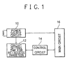
- Fig. 1 shows an embodiment of a non-contact type IC card in accordance with the present invention.
- This IC card is an IC card of an external power supply type receiving power supply from an external device.
- portions not directly related to the present invention are not shown in this embodiment.
- the card has a power source circuit 10.
- the power source circuit 10 is a power supply circuit for transmitting power supplied from a reader-writer to the respective components of the card.
- the power source circuit 10 is coupled with the reader-writer via a magnetic coupling shown in the diagram or a capacitive coupling not shown therein to receive power supplied from the reader-writer.
- the power source circuit 10 is connected to a main circuit 16.
- the main circuit 16 is a circuit accomplishing operations according to various functions of the card and is constituted with a central processing unit (CPU), a memory, etc.
- CPU central processing unit
- memory etc.
- FIG. 5 there are included a memory 32 and a memory control section 36.
- the main circuit 16 has a function to read, when the card is put by the bearer into an area accessible to the reader-writer, ID data from the memory 16 to output the data to the reader-writer and/or a function to collate ID data sent from the reader-writer with data stored in the memory 32. Moreover, the main circuit 16 writes in the memory 32, after the passage of the bearer is admitted by the reader-writer as a result of such a collation of the ID data, an indication that the passage is admitted by the data sent from the reader-writer.
- the card in addition has a re-access inhibition time setting circuit 12.
- the circuit 12 is connected to the power source circuit 10 to set a period of time for inhibiting a re-access based on a voltage supplied from the power source circuit 10 and a control signal sent from the control circuit 14 and then outputs a re-access inhibition time setting signal to the control circuit 14.
- the control circuit 14 is connected to the circuit 12 and the main circuit 16 to inhibit the operation of the main circuit 16 for a predetermined period of time according to the re-access inhibition time setting signal outputted from the circuit 12. Furthermore, the control circuit 14 controls, in accordance with an access operation terminating signal transmitted from the main circuit 16, the setting operation of the circuit 12.
- Fig. 2 shows a more specific construction of the circuit of Fig. 1.
- Four diodes D1, D2, D3, and D4; two capacitors C1 and C2; and a regulator 20 are disposed as elements corresponding to the power source circuit 10 of Fig. 10. Electric energy supplied from the reader-writer via a coil L is rectified by the diodes D1 to D4 and the regulator 20. Alternating-current components are removed therefrom by the capacitors C1 and C2 such that the resultant signal is sent to the main circuit 1 and the re-access inhibition time setting circuit 12.
- the circuit 12 possesses a transistor Q.
- the transistor Q has an emitter region connected to an output of the power source circuit 10 and a base region which is connected via a resistor R2 to the output from the power source 10 and which is connected via a resistor R4 to an output of the control circuit 14.
- the transistor Q has a collector region linked with an anode of the diode D5 having a cathode connected to a resistor R1 and a capacitor C3. Other terminals respectively of the resistor R1 and the capacitor C3 are grounded.
- the cathode of the diode D5 is further connected to a gate region of an field-effect transistor (FET) of an n-type channel 24.
- FET field-effect transistor
- the FET 24 has a drain region which is linked via a resistor R3 to an output of the power source circuit 10 and which is linked to a Schmitt trigger circuit 22, whereas the FET 24 has a source region grounded.
- the Schmitt trigger circuit 22 has an output connected to an input of the control circuit 14.
- the circuit 12 sets an inhibition time for inhibiting the second access.
- power as indicated by A in Fig. 3 is supplied as an output from the power source circuit 10. Namely, when the card enters the accessible area of the reader-writer twice (at points of time t1 and t4), energy is supplied at each point of time from the reader-writer via the power supply circuit 10. When power is supplied at the point A, the power is fed to the main circuit 16, thereby enabling the main circuit 16 to operate.
- the main circuit 16 is powered and a signal B denoting that the main circuit 16 is operable is delivered via the resistor R4 to the base region of the transistor Q (time t1).
- the transistor Q is in a non-conductive state and the power supplied to the point A is not fed to a point C.
- the potential of the point C is hence at a ground level as designated by C in Fig. 3.
- the FET 24 is in a non-conductive state and a point D of the drain region of the FET 24 is supplied with the output from the power source circuit 10 as indicated by D in Fig. 3.
- the output from the Schmitt trigger circuit 22 is also as denoted by E in Fig. 3 and the output E is transmitted to the control circuit 14.
- the control circuit 14 outputs, according to the output E, a signal allowing the operation of the main circuit 16 to the main circuit 16.
- a signal B indicating that power can be supplied to the main circuit 16 is sent from the control circuit 14 to the transistor Q, which sets the transistor Q to a non-conductive state.
- the point C is kept remained in a state where power is not supplied from the power source circuit 10 and hence the potential of the point C continues lowering as shown in Fig. 3.
- the potential of the point D is gradually increased.
- the voltage D inputted to the Schmitt trigger circuit 22 is gradually increased, at a point of time t5 where the voltage D exceeds the predetermined value, a signal E is outputted from the Schmitt trigger circuit 22. According to this output E, the control circuit 14 outputs a signal allowing the operation of the main circuit 16 to the main circuit 16.
- the operation of the main circuit 16 is allowed. Consequently, after the first operation (access to the reader-writer) of the main circuit 16 at the point of time t2 is finished, the operation of the main circuit 16 is not allowed until a point of time t5. In consequence, even in a case where the card is put to the accessible area at the time t4 to supply power from the power source circuit 10, the main circuit 16 does not achieve any operation. As above, after the first access is terminated, the access to the reader-writer can be inhibited for a fixed period of time.
- step 102 Whether or not power is being supplied is judged (step 102). If this is not the case, a wait operation is effected until the power-on state occurs. If the power is being supplied, it is assumed that the card has entered the accessible area of the reader-writer and a check is made to determine whether or not the point of time is during the re-access inhibition period (step 104). If this is the case, whether or not the power is off is judged (step 106). If the power is not off, a wait operation is achieved until the power is turned off. When the power is turned off, it is assumed that the card is removed from the accessible area of the reader-writer and control is returned to the first step 102.
- step 104 if the current point is not in the re-access inhibition period, it is assumed that the access to the reader-writer becomes to be possible and then a predetermined data communication is achieved with the reader-writer (step 108). Whether or not the data communication has been completed is judged (step 110). If this is the case, the re-access inhibition period is set (step 112). Thereafter, whether or not the power is turned off is checked (step 114).
- step 116 determines whether or not the power is turned off.
- the re-access can be inhibited for a fixed period of time.
- the second and subsequent accesses to the reader-writer can be inhibited and hence the inappropriate operation due to a plurality of accesses can be prevented.
- the operation to inhibit the re-access of the card need not be achieved by the reader-writer, thereby minimizing the load imposed on the reader-writer.
- the reader-writer in a case where, for example, it is necessary at a gate to check passages of many cards in a short period of time, the reader-writer is not required to check the re-access. Consequently, after an access of a card, the reader-writer can immediately await a passage of the next card, which enables the accesses to many cards in a smooth manner.
- the operation inhibition signal generating means operates to create an operation inhibition signal, thereby inhibiting the operation of the main circuit means for a predetermined period of time. Consequently, in a case where the card enters an area accessible to the external device a plurality of times in a short period of time, the second and subsequent accesses can be inhibited, thereby preventing the inappropriate operation due to the plural accesses. Furthermore, since the access inhibition above need not be monitored by the external device, the load on the external device can be reduced.
- Fig. 5 shows another embodiment of a non-contact type IC card in accordance with the present invention.
- This card 30 includes a memory 32 of an electrically erasable programmable ROM (EEPROM) or the like.
- the memory 32 has two areas 321 and 322 in this embodiment.
- data items are recorded in these two areas 321 and 322 together with numbers indicating sequence numbers of the data item write operation.
- the data items are read by referencing the numbers in the areas so that data is read from one of the areas last undergone a recording operation.
- the number of areas disposed in the memory 32 is not limited to two, namely, the number may be three or more.
- the card 30 further include a read area deciding section 34 connected to the memory 32.
- the read area deciding section 34 judges to determine from which one of the two areas 321 and 322 of the memory data is to be read.
- the memory 32 and the section 34 are connected to a memory control section 36.
- the section 36 controls according to commands an operation to write in the memory 32 data sent from a reader-writer, not shown, via a noncontact terminal 40 and a modulating and demodulating section 38 and an operation to read data stored in the memory 32 so as to feed the data to the reader-writer.
- the memory control section 36 achieves a control operation to record data sent from the reader-writer alternately in the two areas 321 and 322 together with the numbers indicating the recording order.
- the section 36 controls a data read operation to read data from an area determined by the section 34.
- the modulating and demodulating section 38 modulates data outputted from the memory control section 36 to the reader-writer and demodulates data inputted from the reader-writer via the noncontact terminal 40.
- the terminal 40 is used to communicate data with the reader-writer, not shown, in a noncontact manner.
- the power source circuit 10 is, like in the embodiment described above, a circuit to send power supplied from the reader-writer to the respective sections of the card 30.
- the power source circuit 10 is coupled with the reader-writer via a magnetic coupling shown in the diagram or a capacitive coupling, not shown, to receive power supplied from the reader-writer.
- each of the areas 321 and 322 there are disposed the areas including a data area D in which data is recorded, a number area N in which a number of a write sequence of data is recorded, and a check code area in which a check code is recorded.
- Fig. 6 Immediately after the card 30 is issued, as shown in Fig. 6, there are recorded data 1, "0" as the number denoting the write sequence, and a predetermine code C such as a DDC code in the data areas D, N, and C, respectively.
- the data recorded in the data area D is one of various kinds of data items such as an ID number communicated between the IC card and the reader-writer.
- the number indicating the write sequence recorded in the number area N indicates a write sequential number of data recorded in the data area D of each of two areas.
- "0" is recorded as an initial value.
- the check code recorded in the check code area C is used to determine whether or not the data is normal, and one of the known various codes is employed.
- data inputted from the reader-writer via the noncontact terminal 40 is demodulated by the modulating and demodulating section 38 and is then sent from the memory control section 36 to the memory 32 so as to be stored therein.
- the data to be recorded in the data area D and the code to be recorded in the check code area C are generated by the memory control section 36 and is then sent to the memory 32 to be stored therein.
- a first data write operation is accomplished in the area 322.
- data 2 is recorded in the data area D and a number "1" is recorded as a data record sequential number in the number area N.
- the check code area C there is recorded a predetermined check code.
- the section 34 compares the number recorded in the number area N of the area 321 with that recorded in the number area N of the area 322 to determine that the data recorded in the area 322 is the latest data. Consequently, in the data read operation, the data 2 recorded in the area 322 is read.
- a second data write operation is achieved in the area 321.
- the data write operations are conducted as above in the two areas 321 and 322 in an alternating manner.
- step 202 of Fig. 10 normality or abnormality of the data in the two areas 321 and 322 of the memory 32 is judged by checking the check code by the read area deciding section 34. Whether or not the data of each of the areas 321 and 322 is wrong (NG) is judged (step 204). If this is the case, the section 34 outputs a signal of the condition to the section 36, which then proceeds to the processing of Fig. 11.
- a step 230 of Fig. 11 the section 36 judges to determine whether or not a read operation is to be executed. If this is the case, a signal indicating that the memory 32 is in the destroyed state is outputted from the section 36 to the reader-writer (step 232). Otherwise, whether or not a write operation is to be executed is judged (step 234). If this is the case, data is written in the data area D of the area 321 and a number "0" is recorded in the number area N (Step 236). If the write operation is not assumed in the step 234, control is returned to the step 230 to repeatedly achieve the same operation.
- control is passed to a step 206 such that the section 34 checks to determine whether or not the data in the area 321 is NG. If this is the case, control is transferred to the processing of Fig. 12.
- a step 240 of Fig. 12 the section 36 judges to decide whether or not a read operation is to be executed. If this is the case, data recorded in the area 322 is read to be transmitted to the reader-writer (step 242). Otherwise, whether or not a write operation is to be achieved is judged (step 244). If this is the case, data is written is the data area D of the area 321 and the number to be written in the number area N is updated (step 246). In the step 244, if the write operation is not assumed, control is returned to the step 240 to repeatedly accomplish the same operation.
- control proceeds to a step 208 in which the section 34 judges to determine whether or not the data in the area 322 is NG. If this is the case, control is passed to the processing of Fig. 13.
- the section 36 judges to decide whether or not a read operation is to be executed. If this is the case, data recorded in the area 321 is read to be transmitted to the reader-writer (step 252).
- a write operation data is written in the data area D of the area 322 and a number to be written in the number area N is updated (step 256).
- control is returned to the step 250 to repeatedly accomplish the same operation.
- control proceeds to a step 210 such that the section 34 judges to determine whether or not the number recorded in the number area N of each of the areas is successive. If this is not the case, data of each of the areas is assumed to have been destroyed and control is transferred to the processing of Fig. 11. If the number is consecutive, the number of the area 321 is compared with that of the area 322 (step 212). If the number of the area 321 is larger than that of the area 322, the section 34 assumes that the data recorded in the area 321 is the latest data and then passes control to the processing of Fig. 13 to read data from the area 321. In the step 212, if the number of the area 321 is smaller than that of the area 322, the section 34 assumes that the data recorded in the area 322 is the latest data and then transfers control to the processing of Fig. 12 to read data from the area 322.
- the memory 32 is subdivided into two areas 321 and 322 to record data alternately in these areas with a number indicating a write sequential number assigned to each of the recorded data. In consequence, even when data recorded in one of these areas is wrong, data can be read from the other area and hence the data read operation is not prevented even when an abnormality occurs in the data write operation.
- the card when the card is adopted as a commuter pass or a key for entrance and exit for a place, in a case where the holder moves at a high speed while putting the card in the proximity of the reader-writer, the power supply from the reader-writer is interrupted at an intermediate point of the data write operation and hence the data thus written is wrong.
- data such as the gate check state is kept in the other area; consequently, the disabled state of the data read operation can be avoided by reading the recorded data.
- the memory has an area subdivided into a plurality of areas for storing therein data sent from an external device.
- the data is read from one of the areas in which the data is normally recorded. Consequence, also in a case where data recorded in an area is wrong, data can be read from another area and hence the data read operation is not disabled even when an abnormality takes place in the data write operation.
- Fig. 14 shows further another embodiment of a non-contact type IC card in accordance with the present invention.
- This card includes both configurations of the cards shown in Figs. 1 and 5.
- a re-access can be inhibited for a fixed period of time.
- the card enters an accessible area of the reader-writer two or more times in a short period of time, the second and subsequent accesses to the reader-writer can be inhibited and hence an inappropriate operation due to the plural access can be prevented.
- the card has a function to inhibit the access, the operation to inhibit the re-access of the card need not be accomplished by the reader-writer and hence the load imposed on the reader-writer can be mitigated.
- a memory 32 is subdivided into two areas 321 and 322 such that data is recorded alternately in these areas with a number indicating a write sequence number assigned to the recorded data. Consequently, even when data recorded in one of the areas is wrong, data can be read from the other area and hence the data read operation is not disabled even when an abnormality occurs in the data write operation.
- the respective embodiments have been described in conjunction with non-contact type IC card of an external power supply type to which power is supplied from an external device.
- the present invention is not restricted by the IC card of the external power supply type and is also applicable to an IC card of an integrated power supply type.
- the IC card of the integrated power supply type there is disposed an integrated power source in addition to the power source circuit 10 above.
Landscapes
- Engineering & Computer Science (AREA)
- Physics & Mathematics (AREA)
- General Physics & Mathematics (AREA)
- Theoretical Computer Science (AREA)
- Microelectronics & Electronic Packaging (AREA)
- Computer Networks & Wireless Communication (AREA)
- Business, Economics & Management (AREA)
- Computer Security & Cryptography (AREA)
- Computer Hardware Design (AREA)
- Accounting & Taxation (AREA)
- Strategic Management (AREA)
- General Business, Economics & Management (AREA)
- Credit Cards Or The Like (AREA)
- Storage Device Security (AREA)
- Financial Or Insurance-Related Operations Such As Payment And Settlement (AREA)
Abstract
Description
- The present invention relates to a non-contact type integrated circuit (IC) card not having contact terminals for a power source and for inputting and outputting signals.
- There has been known an IC card which as not contact terminals for receiving signals from an external device or for outputting signals thereto via a magnetic or capacitive coupling therewith. When using the non-contact type IC card, as compared with the card achieving communications of signals via contact terminals, the read operation is facilitated since, for example, when a person having the card in his or her hand approaches the external device, data stored in the card can be read therefrom into the external device. Moreover, there can be prevented such problems associated with the card achieving input and output operations of data via contact terminals as a contact failure due to dirt, erosion, etc. of terminal contact points and wrong operations due to a leakage current.
- For the read operation of the non-contact type IC card, the card bearer having the card with him or her need only approach the reader and there is unnecessitated a read operation to insert the card into the reader. Consequently, the card is suitable for a check of sequential passage of many persons, for example, the card is suitably used as a commuter pass or a key for checking entrance an exit for a particular room.
- In a case where the non-contact type IC card is adopted as a commuter pass or a key for checking entrance and exit for a room, ID data is read from a memory of the IC card for a collation thereof such that when the collation results in a coincidence, the passage of the gate or the entrance for the room is admitted. At the same time, historical data of uses of the IC card is written in the memory thereof.
- When a non-contact type IC card is brought into an area accessible to the reader-writer, the collation and the write operation of the history are accomplished. Since the accessible area has a range of a certain magnitude, when the card is employed as, for example, a commuter pass, there may occur depending on actions of the card holder a case where an identical card enters two or more times the area accessible to the reader-writer installed at the gate. Namely, it may possible occur, the user puts the card into the area, removes the card from the area, and then puts again the card into the area. In such a case, it is necessary to avoid the write operation of history in the second access.
- Conventionally, in the case above, the second access of an identical card is detected by the reader-writer to inhibit the write operation of new data on the card. However, since passage of many cards is required to be checked in a short period of time at the gate, it is necessary for the reader-writer, after an access of a card, to wait for passage of a subsequent card. Consequently, there does not exit any marginal time enough to check the second access.
- In consequence, it is desired that the operation of a card is inhibited for a fixed period of time after a passage thereof. However, in a card not having a power source therein, namely, a card of an external power supply type, an electromagnetic energy supplied from an external device is rectified to obtain a direct-current (dc) voltage necessary for an internal circuit thereof. Consequently, after the external energy supply is interrupted, it is difficult to control the operation inhibition for a fixed period of time. For example, after the external energy supply is stopped, the circuit in the card may be operated by energy resultant from discharge of electric charges accumulated in a smoothing capacitor of the power source circuit. However, since the operation of the circuit is determined by a value of a current consumed by the circuit and the energy accumulated in the smoothing capacitor, it is difficult to set the period for inhibiting the operation.
- Moreover, in such a non-contact type IC card, since the contact (approaching) state between the card and the reader-writer cannot be fixedly established, communications of data and power source become to be unstable in some cases. For example, in a card of the external power supply type which receives supply of power via energy such as an electromagnetic field from an external power source, the card is supplied with power only when the card is in the proximity of the reader-writer. When the card is apart from the reader-writer, the power is not supplied thereto. In consequence, in a case where the bearer of the card puts the card close to the reader-writer to write data received from the reader-writer in the memory of the card, when the contact state is changed because the distance between the card and the reader-writer is increased due to movement or the like of the bearer, the power supply from the reader-writer to the card is interrupted. Consequently, the write operation of data in the memory of the card is stopped at an intermediate point and hence data is stored in the memory in an incomplete state.
- Since such incomplete data is directly stored in the memory, when the data is read therefrom by the reader-writer, it is impossible to accomplish a predetermined check operation. For example, when the card is adopted as a commuter pass, the states of the pass such as a period thereof, a valid period thereof, a station name where the bearer took the train, and time when the bearer took the train are required to be accurate in any case. Otherwise, there arises a problem that the essential object of the card cannot be achieved.
- It is therefore an object of the present invention to provide a non-contact type IC card guaranteeing the normal operation even when an abnormality occurs in an access operation between the card and the external device, thereby solving the problems of the non-contact type IC card.
- Namely, the present invention aims at providing a non-contact type IC card capable of preventing inappropriate data from being written therein even when the card enters an area accessible to the external device for a plurality of times at a short interval of time.
- Moreover, another object of the present invention is to provide a non-contact type IC card guaranteeing the normal operation even when an abnormality occurs in the contact state during a write operation of data from the external device.
- In accordance with the present invention, a non-contact type IC card achieving communications of signals with an external device in a noncontact manner includes main circuit means for conducting various operations based on functions of the IC card, operation inhibition signal generating means for creating an operation inhibition signal to inhibit the operation of the main circuit means for a predetermined period of time, and control means for controlling the main circuit means and the operation inhibition signal generating means. The control means operates the operation inhibition signal generating means when the operation of the main circuit means is finished and inhibits the operation of the main circuit means for a predetermined period of time according to the operation inhibition signal from the operation inhibition signal generating means.
- In accordance with the present invention, when an operation of the main circuit means is finished, the operation inhibition signal generating means operates to create an operation inhibition signal, thereby inhibiting the operation of the main circuit means for a predetermined period of time. In consequence, in a case where the card enters an area accessible to the external device a plurality of times during a short period of time, the second and subsequent accesses can be inhibited and hence the improper operation due to the plural accesses can be avoided. Moreover, since the inhibition of such accesses need not be monitored by the external device, the load imposed on the external device can be minimized.
- In accordance with the present invention, a non-contact type IC card includes communicating means for communicating signals with an external device in a noncontact manner, a memory for storing therein data sent from the external device, and control means for controlling operations of the communicating means and the memory. The memory has an area subdivided into a plurality of areas for storing therein data sent from the external device, and the control means reads, when the data is to be read from the memory, the data from one of the plural areas in which the data is normally stored.
- In accordance with the non-contact type IC card of the present invention, an area of a memory for storing therein data sent from the external device is subdivided into a plurality of areas such that when reading data from the memory, the data is read from an area of the plural areas in which the data is normally stored. In consequence, even when the data recorded in one of the areas is wrong, the data can be read from the other area. Consequently, even when an abnormality occurs in a write operation of data, the data can be read therefrom.
- In consequence, a write operation of wrong data or absence of record data which occurs when the card holder moves therewith at a high speed can be coped with by executing a predetermined processing with the normal data read from the memory.
-
- Fig. 1 is a functional block diagram showing an embodiment of a non-contact type IC card in accordance with the present invention;
- Fig. 2 a circuit diagram showing a specific example of the card of Fig. 1;
- Fig. 3 is a timing chart showing the operation of the circuit of Fig. 2;
- Fig. 4 is a timing chart showing the operation of the control circuit of Fig. 2;
- Fig. 5 is a block diagram showing another embodiment of a non-contact type IC card in accordance with the present invention;
- Fig. 6 shows a write operation of data in a memory of the card of Fig. 5;
- Fig. 7 shows a write operation of data in a memory of the card of Fig. 5;
- Fig. 8 shows a write operation of data in a memory of the card of Fig. 5;
- Fig. 9 shows a write operation of data in a memory of the card of Fig. 5;
- Fig. 10 is a flowchart showing the operation of the card of Fig. 5;
- Fig. 11 is a flowchart showing the operation of the card of Fig. 5;
- Fig. 12 is a flowchart showing the operation of the card of Fig. 5; and
- Fig. 13 is a flowchart showing the operation of the card of Fig. 5
- Referring next to the accompanying drawings, description will be given in detail of a non-contact type IC card in accordance with the present invention.
- Fig. 1 shows an embodiment of a non-contact type IC card in accordance with the present invention. This IC card is an IC card of an external power supply type receiving power supply from an external device. In this connection, portions not directly related to the present invention are not shown in this embodiment.
- The card has a
power source circuit 10. Thepower source circuit 10 is a power supply circuit for transmitting power supplied from a reader-writer to the respective components of the card. Thepower source circuit 10 is coupled with the reader-writer via a magnetic coupling shown in the diagram or a capacitive coupling not shown therein to receive power supplied from the reader-writer. - The
power source circuit 10 is connected to amain circuit 16. Themain circuit 16 is a circuit accomplishing operations according to various functions of the card and is constituted with a central processing unit (CPU), a memory, etc. For example, as shown in Fig. 5, there are included amemory 32 and amemory control section 36. - The
main circuit 16 has a function to read, when the card is put by the bearer into an area accessible to the reader-writer, ID data from thememory 16 to output the data to the reader-writer and/or a function to collate ID data sent from the reader-writer with data stored in thememory 32. Moreover, themain circuit 16 writes in thememory 32, after the passage of the bearer is admitted by the reader-writer as a result of such a collation of the ID data, an indication that the passage is admitted by the data sent from the reader-writer. - The card in addition has a re-access inhibition
time setting circuit 12. Thecircuit 12 is connected to thepower source circuit 10 to set a period of time for inhibiting a re-access based on a voltage supplied from thepower source circuit 10 and a control signal sent from thecontrol circuit 14 and then outputs a re-access inhibition time setting signal to thecontrol circuit 14. - The
control circuit 14 is connected to thecircuit 12 and themain circuit 16 to inhibit the operation of themain circuit 16 for a predetermined period of time according to the re-access inhibition time setting signal outputted from thecircuit 12. Furthermore, thecontrol circuit 14 controls, in accordance with an access operation terminating signal transmitted from themain circuit 16, the setting operation of thecircuit 12. - Fig. 2 shows a more specific construction of the circuit of Fig. 1. Four diodes D1, D2, D3, and D4; two capacitors C1 and C2; and a
regulator 20 are disposed as elements corresponding to thepower source circuit 10 of Fig. 10. Electric energy supplied from the reader-writer via a coil L is rectified by the diodes D1 to D4 and theregulator 20. Alternating-current components are removed therefrom by the capacitors C1 and C2 such that the resultant signal is sent to themain circuit 1 and the re-access inhibitiontime setting circuit 12. - The
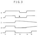
circuit 12 possesses a transistor Q. The transistor Q has an emitter region connected to an output of thepower source circuit 10 and a base region which is connected via a resistor R2 to the output from thepower source 10 and which is connected via a resistor R4 to an output of thecontrol circuit 14. The transistor Q has a collector region linked with an anode of the diode D5 having a cathode connected to a resistor R1 and a capacitor C3. Other terminals respectively of the resistor R1 and the capacitor C3 are grounded. The cathode of the diode D5 is further connected to a gate region of an field-effect transistor (FET) of an n-type channel 24. TheFET 24 has a drain region which is linked via a resistor R3 to an output of thepower source circuit 10 and which is linked to aSchmitt trigger circuit 22, whereas theFET 24 has a source region grounded. TheSchmitt trigger circuit 22 has an output connected to an input of thecontrol circuit 14. - Referring to the timing chart of Fig. 3, the operation of the
circuit 12 will be described. In a case where the card is used as a commuter pass and is put into an accessible area of the reader-writer at a gate twice in a short period of time, thecircuit 12 sets an inhibition time for inhibiting the second access. - At a point A of Fig. 2, power as indicated by A in Fig. 3 is supplied as an output from the
power source circuit 10. Namely, when the card enters the accessible area of the reader-writer twice (at points of time t1 and t4), energy is supplied at each point of time from the reader-writer via thepower supply circuit 10. When power is supplied at the point A, the power is fed to themain circuit 16, thereby enabling themain circuit 16 to operate. During the operation of themain circuit 16, as indicated by B in Fig. 3, themain circuit 16 is powered and a signal B denoting that themain circuit 16 is operable is delivered via the resistor R4 to the base region of the transistor Q (time t1). Consequently, the transistor Q is in a non-conductive state and the power supplied to the point A is not fed to a point C. The potential of the point C is hence at a ground level as designated by C in Fig. 3. In consequence, since any signal is not inputted to the gate region of theFET 24, theFET 24 is in a non-conductive state and a point D of the drain region of theFET 24 is supplied with the output from thepower source circuit 10 as indicated by D in Fig. 3. As a result, the output from theSchmitt trigger circuit 22 is also as denoted by E in Fig. 3 and the output E is transmitted to thecontrol circuit 14. Thecontrol circuit 14 outputs, according to the output E, a signal allowing the operation of themain circuit 16 to themain circuit 16. - When the operation of the
main circuit 16 is finished (time t2), the output of the signal B from thecontrol circuit 14 is stopped. This sets the base region of the transistor Q to a low level and hence the transistor Q becomes to be conductive, which increases the potential at the point C as denoted by C in Fig. 3. At the time t3 when the power supply A from thepower source circuit 10 is interrupted, the power from thepower source circuit 10 is not supplied to the point C. However, according to a discharging operation of electric charge accumulated in the capacitor C3 during the power supply period, the potential of the point C is gradually decreased in accordance with the time constant of the capacitor and the resistor as indicated by C in Fig. 3. - At a point of time T4, when the card is again put into the accessible area of the reader-writer and the second power is supplied from the
power source circuit 10, a signal B indicating that power can be supplied to themain circuit 16 is sent from thecontrol circuit 14 to the transistor Q, which sets the transistor Q to a non-conductive state. In consequence, the point C is kept remained in a state where power is not supplied from thepower source circuit 10 and hence the potential of the point C continues lowering as shown in Fig. 3. As a result, since the potential inputted to the gate region of theFET 24 continues decreasing and the current flowing from the drain region to the source region of theFET 24 is minimized, the potential of the point D is gradually increased. In consequence, the voltage D inputted to theSchmitt trigger circuit 22 is gradually increased, at a point of time t5 where the voltage D exceeds the predetermined value, a signal E is outputted from theSchmitt trigger circuit 22. According to this output E, thecontrol circuit 14 outputs a signal allowing the operation of themain circuit 16 to themain circuit 16. - As above, after the output E from the
Schmitt trigger circuit 22 is set to a high level, the operation of themain circuit 16 is allowed. Consequently, after the first operation (access to the reader-writer) of themain circuit 16 at the point of time t2 is finished, the operation of themain circuit 16 is not allowed until a point of time t5. In consequence, even in a case where the card is put to the accessible area at the time t4 to supply power from thepower source circuit 10, themain circuit 16 does not achieve any operation. As above, after the first access is terminated, the access to the reader-writer can be inhibited for a fixed period of time. - Subsequently, the operation of the
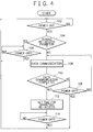
control circuit 14 will be described by reference to the flowchart of Fig. 4. Whether or not power is being supplied is judged (step 102). If this is not the case, a wait operation is effected until the power-on state occurs. If the power is being supplied, it is assumed that the card has entered the accessible area of the reader-writer and a check is made to determine whether or not the point of time is during the re-access inhibition period (step 104). If this is the case, whether or not the power is off is judged (step 106). If the power is not off, a wait operation is achieved until the power is turned off. When the power is turned off, it is assumed that the card is removed from the accessible area of the reader-writer and control is returned to thefirst step 102. - In the
step 104, if the current point is not in the re-access inhibition period, it is assumed that the access to the reader-writer becomes to be possible and then a predetermined data communication is achieved with the reader-writer (step 108). Whether or not the data communication has been completed is judged (step 110). If this is the case, the re-access inhibition period is set (step 112). Thereafter, whether or not the power is turned off is checked (step 114). - If the power is not turned off, a wait operation is executed until the power is turned off. When the power is turned off, it is assumed that the card is removed from the accessible area of the reader-writer and then control is returned to the
first step 102. - Also in the case where the data communication is not completed in the
step 110, whether or not the power is turned off is judged (step 116) such that if this is the case, control is passed to thestep 102. - As above, in accordance with the card of the present embodiment, after an access is finished, the re-access can be inhibited for a fixed period of time. In consequence, in a case where the card enters the accessible area of the reader-writer two or more times in a short period of time, the second and subsequent accesses to the reader-writer can be inhibited and hence the inappropriate operation due to a plurality of accesses can be prevented. Moreover, since the card has the function to inhibit the access, the operation to inhibit the re-access of the card need not be achieved by the reader-writer, thereby minimizing the load imposed on the reader-writer.
- In accordance with the card, in a case where, for example, it is necessary at a gate to check passages of many cards in a short period of time, the reader-writer is not required to check the re-access. Consequently, after an access of a card, the reader-writer can immediately await a passage of the next card, which enables the accesses to many cards in a smooth manner.
- In accordance with the present invention as described above, when the operation of the main circuit means is terminated, the operation inhibition signal generating means operates to create an operation inhibition signal, thereby inhibiting the operation of the main circuit means for a predetermined period of time. Consequently, in a case where the card enters an area accessible to the external device a plurality of times in a short period of time, the second and subsequent accesses can be inhibited, thereby preventing the inappropriate operation due to the plural accesses. Furthermore, since the access inhibition above need not be monitored by the external device, the load on the external device can be reduced.
- Fig. 5 shows another embodiment of a non-contact type IC card in accordance with the present invention. This
card 30 includes amemory 32 of an electrically erasable programmable ROM (EEPROM) or the like. Thememory 32 has twoareas areas areas memory 32 is not limited to two, namely, the number may be three or more. - The
card 30 further include a readarea deciding section 34 connected to thememory 32. The readarea deciding section 34 judges to determine from which one of the twoareas memory 32 and thesection 34 are connected to amemory control section 36. Thesection 36 controls according to commands an operation to write in thememory 32 data sent from a reader-writer, not shown, via anoncontact terminal 40 and a modulating anddemodulating section 38 and an operation to read data stored in thememory 32 so as to feed the data to the reader-writer. Thememory control section 36 achieves a control operation to record data sent from the reader-writer alternately in the twoareas section 36 controls a data read operation to read data from an area determined by thesection 34. - The modulating and
demodulating section 38 modulates data outputted from thememory control section 36 to the reader-writer and demodulates data inputted from the reader-writer via thenoncontact terminal 40. The terminal 40 is used to communicate data with the reader-writer, not shown, in a noncontact manner. - The
power source circuit 10 is, like in the embodiment described above, a circuit to send power supplied from the reader-writer to the respective sections of thecard 30. Thepower source circuit 10 is coupled with the reader-writer via a magnetic coupling shown in the diagram or a capacitive coupling, not shown, to receive power supplied from the reader-writer. - Referring to the changes in the recording state of the
memory 32 shown in Figs. 6 to 9, description will be given of the operation to write data in thememory 32. In each of theareas - Immediately after the
card 30 is issued, as shown in Fig. 6, there are recordeddata 1, "0" as the number denoting the write sequence, and a predetermine code C such as a DDC code in the data areas D, N, and C, respectively. The data recorded in the data area D is one of various kinds of data items such as an ID number communicated between the IC card and the reader-writer. The number indicating the write sequence recorded in the number area N indicates a write sequential number of data recorded in the data area D of each of two areas. As shown in Fig. 6, immediately after the issuance of thecard 30, "0" is recorded as an initial value. - The check code recorded in the check code area C is used to determine whether or not the data is normal, and one of the known various codes is employed.
- For the data to be recorded in the data area D, data inputted from the reader-writer via the
noncontact terminal 40 is demodulated by the modulating anddemodulating section 38 and is then sent from thememory control section 36 to thememory 32 so as to be stored therein. Moreover, the data to be recorded in the data area D and the code to be recorded in the check code area C are generated by thememory control section 36 and is then sent to thememory 32 to be stored therein. - Immediately after the issuance of the
card 30, any data is not recorded in thearea 322. Consequently, in a data read operation, the data in thearea 322 is assumed to be in a destroyed state by the readarea deciding section 34 such that data recorded in thearea 321 is read by thememory control section 36. - Next, as shown in Fig. 7, a first data write operation is accomplished in the
area 322. As shown in this diagram,data 2 is recorded in the data area D and a number "1" is recorded as a data record sequential number in the number area N. In the check code area C, there is recorded a predetermined check code. In a state in which the first data write operation has been conducted, thesection 34 compares the number recorded in the number area N of thearea 321 with that recorded in the number area N of thearea 322 to determine that the data recorded in thearea 322 is the latest data. Consequently, in the data read operation, thedata 2 recorded in thearea 322 is read. - In addition, as shown in Fig. 8, a second data write operation is achieved in the
area 321. The data write operations are conducted as above in the twoareas - As a result of the second data write operation of Fig. 8, in the
area 321,data 3 is recorded in the data area D, a number "2" is recorded as a data record sequential number in the number area N, and a predetermined check code is recorded in the check code area C. In a state where the second data write operation is achieved as above, the data recorded in thearea 321 is the latest data and hence thedata 3 recorded in thearea 321 is read in the data read operation. - Subsequently, in a similar manner, data write operations are conducted in the two
areas area 322, if the (n + 1)-th data write operation in thearea 321 results in a failure, the data in thearea 321 is in the destroyed state. Consequently, in this case, the readarea deciding section 34 assumes, without achieving the comparison between the numbers stored in the number areas N of the two areas, that the data recorded in thearea 322 is the latest data such that the data is read by thememory control unit 36. - Subsequently, the operation of the
IC card 30 will be described according to the flowcharts shown in Figs. 10 to 13. - First, in a
step 202 of Fig. 10, normality or abnormality of the data in the twoareas memory 32 is judged by checking the check code by the readarea deciding section 34. Whether or not the data of each of theareas section 34 outputs a signal of the condition to thesection 36, which then proceeds to the processing of Fig. 11. - In a
step 230 of Fig. 11, thesection 36 judges to determine whether or not a read operation is to be executed. If this is the case, a signal indicating that thememory 32 is in the destroyed state is outputted from thesection 36 to the reader-writer (step 232). Otherwise, whether or not a write operation is to be executed is judged (step 234). If this is the case, data is written in the data area D of thearea 321 and a number "0" is recorded in the number area N (Step 236). If the write operation is not assumed in thestep 234, control is returned to thestep 230 to repeatedly achieve the same operation. - In the
step 204 of Fig. 10, if data of both of the twoareas step 206 such that thesection 34 checks to determine whether or not the data in thearea 321 is NG. If this is the case, control is transferred to the processing of Fig. 12. - In a
step 240 of Fig. 12, thesection 36 judges to decide whether or not a read operation is to be executed. If this is the case, data recorded in thearea 322 is read to be transmitted to the reader-writer (step 242). Otherwise, whether or not a write operation is to be achieved is judged (step 244). If this is the case, data is written is the data area D of thearea 321 and the number to be written in the number area N is updated (step 246). In thestep 244, if the write operation is not assumed, control is returned to thestep 240 to repeatedly accomplish the same operation. - In the
step 206 of Fig. 10, when the data in thearea 321 is not NG, control proceeds to astep 208 in which thesection 34 judges to determine whether or not the data in thearea 322 is NG. If this is the case, control is passed to the processing of Fig. 13. In astep 250 of Fig. 13, thesection 36 judges to decide whether or not a read operation is to be executed. If this is the case, data recorded in thearea 321 is read to be transmitted to the reader-writer (step 252). In the case of a write operation, data is written in the data area D of thearea 322 and a number to be written in the number area N is updated (step 256). In thestep 254, when the write operation is not assumed, control is returned to thestep 250 to repeatedly accomplish the same operation. - In the
step 208 of Fig. 10, when the data in thearea 322 is not NG, control proceeds to astep 210 such that thesection 34 judges to determine whether or not the number recorded in the number area N of each of the areas is successive. If this is not the case, data of each of the areas is assumed to have been destroyed and control is transferred to the processing of Fig. 11. If the number is consecutive, the number of thearea 321 is compared with that of the area 322 (step 212). If the number of thearea 321 is larger than that of thearea 322, thesection 34 assumes that the data recorded in thearea 321 is the latest data and then passes control to the processing of Fig. 13 to read data from thearea 321. In thestep 212, if the number of thearea 321 is smaller than that of thearea 322, thesection 34 assumes that the data recorded in thearea 322 is the latest data and then transfers control to the processing of Fig. 12 to read data from thearea 322. - As above, according to the IC card of the present embodiment, the
memory 32 is subdivided into twoareas - For example, when the card is adopted as a commuter pass or a key for entrance and exit for a place, in a case where the holder moves at a high speed while putting the card in the proximity of the reader-writer, the power supply from the reader-writer is interrupted at an intermediate point of the data write operation and hence the data thus written is wrong. However, also in such a case, data such as the gate check state is kept in the other area; consequently, the disabled state of the data read operation can be avoided by reading the recorded data.
- In addition, when the data recorded in each of the areas is normal, the numbers recorded in the number areas N of the two areas are compared with each other to select and to read the last recorded data. Consequently, although data items are recorded in two areas, it will not occur that the old data is read by mistake.
- In accordance with the non-contact type IC card of the present invention, the memory has an area subdivided into a plurality of areas for storing therein data sent from an external device. In a case of an operation to read data from the memory, the data is read from one of the areas in which the data is normally recorded. Consequence, also in a case where data recorded in an area is wrong, data can be read from another area and hence the data read operation is not disabled even when an abnormality takes place in the data write operation.
- Consequently, a write operation of wrong data and absence of record data caused, for example, when the card holder moves at a high speed with the card can be coped with by reading the normal data so as to conduct a predetermined processing.
- Fig. 14 shows further another embodiment of a non-contact type IC card in accordance with the present invention. This card includes both configurations of the cards shown in Figs. 1 and 5. According to this card, as can be appreciated from the explanation above, after an access is finished, a re-access can be inhibited for a fixed period of time. In consequence, when the card enters an accessible area of the reader-writer two or more times in a short period of time, the second and subsequent accesses to the reader-writer can be inhibited and hence an inappropriate operation due to the plural access can be prevented. Moreover, since the card has a function to inhibit the access, the operation to inhibit the re-access of the card need not be accomplished by the reader-writer and hence the load imposed on the reader-writer can be mitigated.
- Furthermore, a
memory 32 is subdivided into twoareas - Moreover, in a case where data written in each of the areas is normal, the numbers recorded in the number areas N of the two areas are compared with each other so as to select and to read the latest record data. Consequently, although data items are recorded in two areas, the old data cannot be read by mistake.
- In this regard, the respective embodiments have been described in conjunction with non-contact type IC card of an external power supply type to which power is supplied from an external device. However, the present invention is not restricted by the IC card of the external power supply type and is also applicable to an IC card of an integrated power supply type. In a case of the IC card of the integrated power supply type, there is disposed an integrated power source in addition to the
power source circuit 10 above.
Claims (4)
- A non-contact type IC card, comprising:communicating means for communicating signals with an external device in a noncontact manner;a memory for storing therein data sent from the external device; andcontrol means for controlling operations of the communicating means and the memory,characterized in that:the memory has an area subdivided into a plurality of areas for storing therein data sent from the external device; andthe control means reads, when the data is to be read from the memory, the data from one of the plural areas in which the data is normally stored.
- A non-contact type IC card in accordance with claim 1, characterized in that the control means reads, when there are a plurality of areas in which the data is normally stored, the data from one of the areas in which the data is last stored.
- A non-contact type IC card in accordance with claim 2, characterized in that number data indicating a recording sequence number of the data is recorded in each of the plural areas of the memory.
- A non-contact type IC card in accordance with claim 1, 2, or 3, characterized by further including a power source circuit for receiving power from an external device and supplying the power to each section of the card.
Applications Claiming Priority (7)
| Application Number | Priority Date | Filing Date | Title |
|---|---|---|---|
| JP14676091 | 1991-05-22 | ||
| JP146760/91 | 1991-05-22 | ||
| JP3146760A JPH04344993A (en) | 1991-05-22 | 1991-05-22 | Non-contact type ic card |
| JP3169169A JP2942809B2 (en) | 1991-06-14 | 1991-06-14 | Non-contact IC card |
| JP169169/91 | 1991-06-14 | ||
| JP16916991 | 1991-06-14 | ||
| EP92910459A EP0541818B1 (en) | 1991-05-22 | 1992-05-21 | Non-contact type ic card |
Related Parent Applications (2)
| Application Number | Title | Priority Date | Filing Date |
|---|---|---|---|
| EP92910459A Division EP0541818B1 (en) | 1991-05-22 | 1992-05-21 | Non-contact type ic card |
| EP92910459.4 Division | 1992-12-04 |
Publications (3)
| Publication Number | Publication Date |
|---|---|
| EP0786737A2 true EP0786737A2 (en) | 1997-07-30 |
| EP0786737A3 EP0786737A3 (en) | 2000-11-02 |
| EP0786737B1 EP0786737B1 (en) | 2003-04-16 |
Family
ID=26477497
Family Applications (2)
| Application Number | Title | Priority Date | Filing Date |
|---|---|---|---|
| EP97105219A Expired - Lifetime EP0786737B1 (en) | 1991-05-22 | 1992-05-21 | Non-contact type IC card |
| EP92910459A Expired - Lifetime EP0541818B1 (en) | 1991-05-22 | 1992-05-21 | Non-contact type ic card |
Family Applications After (1)
| Application Number | Title | Priority Date | Filing Date |
|---|---|---|---|
| EP92910459A Expired - Lifetime EP0541818B1 (en) | 1991-05-22 | 1992-05-21 | Non-contact type ic card |
Country Status (5)
| Country | Link |
|---|---|
| US (1) | US5378887A (en) |
| EP (2) | EP0786737B1 (en) |
| CA (1) | CA2087611C (en) |
| DE (2) | DE69223381T2 (en) |
| WO (1) | WO1992021104A1 (en) |
Families Citing this family (27)
| Publication number | Priority date | Publication date | Assignee | Title |
|---|---|---|---|---|
| WO1993011509A1 (en) † | 1991-12-04 | 1993-06-10 | Citizen Watch Co., Ltd. | Data carrier |
| JP2891136B2 (en) * | 1994-07-19 | 1999-05-17 | 株式会社デンソー | In-vehicle equipment with automatic toll collection system |
| JP2907048B2 (en) * | 1995-02-17 | 1999-06-21 | 株式会社デンソー | Mobile communication roadside unit, mobile communication mobile unit, and mobile communication system |
| US5847447A (en) * | 1996-07-09 | 1998-12-08 | Ambient Corporation | Capcitively coupled bi-directional data and power transmission system |
| US5812942A (en) * | 1996-09-24 | 1998-09-22 | Motorola, Inc. | Balanced differential radio receiver and method of operation |
| US5815020A (en) * | 1996-09-24 | 1998-09-29 | Motorola, Inc. | Balance differential receiver |
| JPH10135882A (en) * | 1996-10-24 | 1998-05-22 | Toshiba Corp | Contactless information recording medium and its data transmission system |
| US6164532A (en) * | 1997-05-15 | 2000-12-26 | Hitachi, Ltd. | Power transmission system, power transmission/communication system and reader and/or writer |
| US5963144A (en) * | 1997-05-30 | 1999-10-05 | Single Chip Systems Corp. | Cloaking circuit for use in a radiofrequency identification and method of cloaking RFID tags to increase interrogation reliability |
| JP3721725B2 (en) * | 1997-07-09 | 2005-11-30 | ソニー株式会社 | Information processing method and information processing apparatus |
| US6074312A (en) * | 1997-07-28 | 2000-06-13 | Dynamic Solutions International | Golf handicap system and methods |
| US6079619A (en) * | 1997-08-05 | 2000-06-27 | Denso Corporation | Identification tag for wireless communication with remote controller |
| JP3824451B2 (en) * | 1999-07-29 | 2006-09-20 | 富士通株式会社 | Non-contact IC card presence / absence detection circuit |
| US6362972B1 (en) | 2000-04-13 | 2002-03-26 | Molex Incorporated | Contactless interconnection system |
| US6612852B1 (en) | 2000-04-13 | 2003-09-02 | Molex Incorporated | Contactless interconnection system |
| JP4208557B2 (en) * | 2002-11-28 | 2009-01-14 | キヤノン株式会社 | Contactless communication method card |
| JP3988995B2 (en) * | 2003-03-14 | 2007-10-10 | ソニー・エリクソン・モバイルコミュニケーションズ株式会社 | Information processing apparatus and method, recording medium, and program |
| JP4717381B2 (en) * | 2004-06-11 | 2011-07-06 | 株式会社エヌ・ティ・ティ・ドコモ | Mobile device and access control method |
| US7581678B2 (en) | 2005-02-22 | 2009-09-01 | Tyfone, Inc. | Electronic transaction card |
| EP1959377A4 (en) * | 2005-11-16 | 2009-12-02 | Kyodo Printing Co Ltd | Noncontact ic card |
| JP4235236B2 (en) * | 2006-09-12 | 2009-03-11 | 東芝テック株式会社 | Wireless communication device |
| EP2009575B1 (en) * | 2007-06-27 | 2013-06-12 | Research In Motion Limited | System and method for improving smart card reader reconnections |
| US9741027B2 (en) | 2007-12-14 | 2017-08-22 | Tyfone, Inc. | Memory card based contactless devices |
| US8451122B2 (en) | 2008-08-08 | 2013-05-28 | Tyfone, Inc. | Smartcard performance enhancement circuits and systems |
| US7961101B2 (en) | 2008-08-08 | 2011-06-14 | Tyfone, Inc. | Small RFID card with integrated inductive element |
| US20100033310A1 (en) * | 2008-08-08 | 2010-02-11 | Narendra Siva G | Power negotation for small rfid card |
| US8231061B2 (en) | 2009-02-24 | 2012-07-31 | Tyfone, Inc | Contactless device with miniaturized antenna |
Citations (2)
| Publication number | Priority date | Publication date | Assignee | Title |
|---|---|---|---|---|
| JPS62234459A (en) * | 1986-04-04 | 1987-10-14 | Casio Comput Co Ltd | Electronic blackboard device |
| EP0282926A2 (en) * | 1987-03-16 | 1988-09-21 | Omron Tateisi Electronics Co. | ID system and method of writing data in an ID system |
Family Cites Families (22)
| Publication number | Priority date | Publication date | Assignee | Title |
|---|---|---|---|---|
| IT1063465B (en) * | 1976-11-03 | 1985-02-11 | Mesdan Spa | AUTOMATIC KNOTTER FOR THE FORMATION OF THE FISHER'S KNOT PARTICULARLY FOR LARGE TITLE YARNS |
| JPS5737228Y2 (en) * | 1976-12-23 | 1982-08-17 | ||
| JPS6168681A (en) * | 1984-09-12 | 1986-04-09 | Toshiba Corp | Portable medium |
| JPS61273689A (en) * | 1985-05-29 | 1986-12-03 | Toppan Moore Co Ltd | Integrated circuit card containing discriminating means between history information and replacement information |
| GB8522418D0 (en) * | 1985-09-10 | 1985-10-16 | Shorrock Security Systems Ltd | Non-contact personal identification system |
| JP2557838B2 (en) * | 1986-02-18 | 1996-11-27 | 株式会社東芝 | IC card |
| JPS62287389A (en) * | 1986-06-05 | 1987-12-14 | Omron Tateisi Electronics Co | Id card |
| JPS63273979A (en) * | 1987-05-06 | 1988-11-11 | Mitsubishi Electric Corp | Non-contact card system |
| JPS6482194A (en) * | 1987-09-24 | 1989-03-28 | Fuji Electric Co Ltd | Non-contact communication device for contact identification card |
| JPH01123269U (en) * | 1988-02-16 | 1989-08-22 | ||
| JPH02226390A (en) * | 1989-02-27 | 1990-09-07 | Omron Tateisi Electron Co | Transponding card |
| JP2645163B2 (en) * | 1990-03-13 | 1997-08-25 | 三菱電機株式会社 | Non-contact IC card |
| JP2822624B2 (en) * | 1990-07-03 | 1998-11-11 | 三菱電機株式会社 | Non-contact IC card |
| JP2549189B2 (en) * | 1990-07-17 | 1996-10-30 | 三菱電機株式会社 | IC card |
| JPH04113489A (en) * | 1990-09-04 | 1992-04-14 | Mitsubishi Electric Corp | Non-contact ic card |
| US5191192A (en) * | 1990-09-10 | 1993-03-02 | Mitsubishi Denki Kabushiki Kaisha | Non-contact type information card and communication system |
| JP2549192B2 (en) * | 1990-09-19 | 1996-10-30 | 三菱電機株式会社 | Non-contact IC card and method of using the same |
| JP2872793B2 (en) * | 1990-10-01 | 1999-03-24 | 株式会社日立製作所 | IC card |
| JPH04171592A (en) * | 1990-11-06 | 1992-06-18 | Mitsubishi Electric Corp | Non-contact type information card |
| JP2543440B2 (en) * | 1990-12-17 | 1996-10-16 | 三菱電機株式会社 | IC card and IC card system |
| EP0492482B1 (en) * | 1990-12-28 | 1996-10-23 | Mitsubishi Denki Kabushiki Kaisha | Non contact type IC-card |
| JP3027019B2 (en) * | 1991-03-26 | 2000-03-27 | 東京エレクトロン株式会社 | Heat treatment equipment |
-
1992
- 1992-05-21 DE DE69223381T patent/DE69223381T2/en not_active Expired - Fee Related
- 1992-05-21 CA CA002087611A patent/CA2087611C/en not_active Expired - Fee Related
- 1992-05-21 US US07/961,882 patent/US5378887A/en not_active Expired - Lifetime
- 1992-05-21 DE DE69233019T patent/DE69233019T2/en not_active Expired - Fee Related
- 1992-05-21 EP EP97105219A patent/EP0786737B1/en not_active Expired - Lifetime
- 1992-05-21 EP EP92910459A patent/EP0541818B1/en not_active Expired - Lifetime
- 1992-05-21 WO PCT/JP1992/000653 patent/WO1992021104A1/en active IP Right Grant
Patent Citations (2)
| Publication number | Priority date | Publication date | Assignee | Title |
|---|---|---|---|---|
| JPS62234459A (en) * | 1986-04-04 | 1987-10-14 | Casio Comput Co Ltd | Electronic blackboard device |
| EP0282926A2 (en) * | 1987-03-16 | 1988-09-21 | Omron Tateisi Electronics Co. | ID system and method of writing data in an ID system |
Non-Patent Citations (1)
| Title |
|---|
| PATENT ABSTRACTS OF JAPAN vol. 012, no. 106 (E-596), 6 April 1988 (1988-04-06) & JP 62 234459 A (CASIO COMPUT CO LTD), 14 October 1987 (1987-10-14) * |
Also Published As
| Publication number | Publication date |
|---|---|
| US5378887A (en) | 1995-01-03 |
| DE69223381T2 (en) | 1998-06-10 |
| CA2087611C (en) | 1996-09-17 |
| EP0541818A4 (en) | 1994-08-24 |
| DE69233019T2 (en) | 2004-02-05 |
| EP0541818A1 (en) | 1993-05-19 |
| EP0786737B1 (en) | 2003-04-16 |
| EP0786737A3 (en) | 2000-11-02 |
| DE69233019D1 (en) | 2003-05-22 |
| DE69223381D1 (en) | 1998-01-15 |
| WO1992021104A1 (en) | 1992-11-26 |
| EP0541818B1 (en) | 1997-12-03 |
Similar Documents
| Publication | Publication Date | Title |
|---|---|---|
| EP0541818B1 (en) | Non-contact type ic card | |
| US4795898A (en) | Personal memory card having a contactless interface using differential data transfer | |
| US4798322A (en) | Card reader/writer station for use with a personal memory card using differential data transfer | |
| US6462647B1 (en) | Rechargeable active transponder | |
| EP0762321B1 (en) | Non contact IC card system | |
| EP0475716B1 (en) | Non-contact type information card and communication system | |
| KR100593272B1 (en) | Minimum voltage radio frequency identification | |
| JP3631958B2 (en) | Non-contact proximity automatic data collection system and method | |
| EP1012784B1 (en) | Data transaction device having contact and contactless modes of operation | |
| EP1042731B1 (en) | Contact/contactless smart card having customizable antenna interface | |
| KR100275167B1 (en) | Chip card with field strength detector | |
| US7000835B2 (en) | Noncontact type IC card and system thereof | |
| US5999713A (en) | Chip card with a contactless energy supply and data transmission devices | |
| GB2197107A (en) | Communicating with a data-storing device | |
| KR19980081575A (en) | Smart card with adjustable level of external input voltage | |
| EP0159530B1 (en) | Card reader | |
| JP2002064402A (en) | Non-contact transponder | |
| US20040180637A1 (en) | Wireless communication IC and wireless communication information storage medium using the same | |
| JPH06511342A (en) | Communication method between twin contact chip card and card reader | |
| EP1083517A2 (en) | Data processing device for switching between terminal mode and RF mode with a digital circuit | |
| JP2942809B2 (en) | Non-contact IC card | |
| JP3497527B2 (en) | Data carrier communication control system | |
| JP2002222399A (en) | Non-contact ic card | |
| JP2003076964A (en) | Non-contact id tag | |
| JPH06101870B2 (en) | Card-based control system |
Legal Events
| Date | Code | Title | Description |
|---|---|---|---|
| PUAI | Public reference made under article 153(3) epc to a published international application that has entered the european phase |
Free format text: ORIGINAL CODE: 0009012 |
|
| AC | Divisional application: reference to earlier application |
Ref document number: 541818 Country of ref document: EP |
|
| AK | Designated contracting states |
Kind code of ref document: A2 Designated state(s): DE FR GB |
|
| PUAL | Search report despatched |
Free format text: ORIGINAL CODE: 0009013 |
|
| AK | Designated contracting states |
Kind code of ref document: A3 Designated state(s): DE FR GB |
|
| 17P | Request for examination filed |
Effective date: 20010305 |
|
| 17Q | First examination report despatched |
Effective date: 20011012 |
|
| GRAH | Despatch of communication of intention to grant a patent |
Free format text: ORIGINAL CODE: EPIDOS IGRA |
|
| GRAH | Despatch of communication of intention to grant a patent |
Free format text: ORIGINAL CODE: EPIDOS IGRA |
|
| GRAA | (expected) grant |
Free format text: ORIGINAL CODE: 0009210 |
|
| AC | Divisional application: reference to earlier application |
Ref document number: 0541818 Country of ref document: EP Kind code of ref document: P |
|
| AK | Designated contracting states |
Designated state(s): DE FR GB |
|
| REG | Reference to a national code |
Ref country code: GB Ref legal event code: FG4D |
|
| REF | Corresponds to: |
Ref document number: 69233019 Country of ref document: DE Date of ref document: 20030522 Kind code of ref document: P |
|
| ET | Fr: translation filed | ||
| PLBE | No opposition filed within time limit |
Free format text: ORIGINAL CODE: 0009261 |
|
| STAA | Information on the status of an ep patent application or granted ep patent |
Free format text: STATUS: NO OPPOSITION FILED WITHIN TIME LIMIT |
|
| 26N | No opposition filed |
Effective date: 20040119 |
|
| PGFP | Annual fee paid to national office [announced via postgrant information from national office to epo] |
Ref country code: FR Payment date: 20060519 Year of fee payment: 15 |
|
| PGFP | Annual fee paid to national office [announced via postgrant information from national office to epo] |
Ref country code: GB Payment date: 20060524 Year of fee payment: 15 |
|
| PGFP | Annual fee paid to national office [announced via postgrant information from national office to epo] |
Ref country code: DE Payment date: 20060731 Year of fee payment: 15 |
|
| GBPC | Gb: european patent ceased through non-payment of renewal fee |
Effective date: 20070521 |
|
| REG | Reference to a national code |
Ref country code: FR Ref legal event code: ST Effective date: 20080131 |
|
| PG25 | Lapsed in a contracting state [announced via postgrant information from national office to epo] |
Ref country code: DE Free format text: LAPSE BECAUSE OF NON-PAYMENT OF DUE FEES Effective date: 20071201 |
|
| PG25 | Lapsed in a contracting state [announced via postgrant information from national office to epo] |
Ref country code: GB Free format text: LAPSE BECAUSE OF NON-PAYMENT OF DUE FEES Effective date: 20070521 |
|
| PG25 | Lapsed in a contracting state [announced via postgrant information from national office to epo] |
Ref country code: FR Free format text: LAPSE BECAUSE OF NON-PAYMENT OF DUE FEES Effective date: 20070531 |