EP0782077A1 - Procédé et arrangement pour convertir des adresses de mémoire en signaux de commande de mémoire - Google Patents
Procédé et arrangement pour convertir des adresses de mémoire en signaux de commande de mémoire Download PDFInfo
- Publication number
- EP0782077A1 EP0782077A1 EP96119487A EP96119487A EP0782077A1 EP 0782077 A1 EP0782077 A1 EP 0782077A1 EP 96119487 A EP96119487 A EP 96119487A EP 96119487 A EP96119487 A EP 96119487A EP 0782077 A1 EP0782077 A1 EP 0782077A1
- Authority
- EP
- European Patent Office
- Prior art keywords
- memory
- capacity
- information
- logical
- configuration information
- Prior art date
- Legal status (The legal status is an assumption and is not a legal conclusion. Google has not performed a legal analysis and makes no representation as to the accuracy of the status listed.)
- Granted
Links
Images


Classifications
-
- G—PHYSICS
- G06—COMPUTING; CALCULATING OR COUNTING
- G06F—ELECTRIC DIGITAL DATA PROCESSING
- G06F12/00—Accessing, addressing or allocating within memory systems or architectures
- G06F12/02—Addressing or allocation; Relocation
- G06F12/06—Addressing a physical block of locations, e.g. base addressing, module addressing, memory dedication
- G06F12/0646—Configuration or reconfiguration
- G06F12/0684—Configuration or reconfiguration with feedback, e.g. presence or absence of unit detected by addressing, overflow detection
-
- G—PHYSICS
- G06—COMPUTING; CALCULATING OR COUNTING
- G06F—ELECTRIC DIGITAL DATA PROCESSING
- G06F12/00—Accessing, addressing or allocating within memory systems or architectures
- G06F12/02—Addressing or allocation; Relocation
- G06F12/06—Addressing a physical block of locations, e.g. base addressing, module addressing, memory dedication
- G06F12/0646—Configuration or reconfiguration
- G06F12/0653—Configuration or reconfiguration with centralised address assignment
Definitions
- a memory usually dynamic or static RAM's (Random Access Memory) - is provided for storing programs and data.
- the processor In order to write data into memory areas of the memory or to read data from the individual memory areas, the processor generates a memory area address and transfers it to a memory controller - known in the art as SRAM or DRAM controller.
- the memory controller forwards this memory area address via address lines to address inputs of the memory.
- the memory area addresses usually represent a dual number, the smallest addressable memory area usually comprising one or more bytes.
- the memory is formed by a plurality of insertion areas, in each of which at least one memory module - usually an integrated memory module - can be inserted.
- the application areas realized by plug-in devices are often designed in such a way that memory modules or memory modules with different memory capacities can be used - for example memory modules with 1 or 4 Kbytes or Mbytes.
- By fitting the application areas differently an optimal adaptation of the storage capacity of the memory to the respective application is possible.
- the memory modules depending on their memory capacity, have to be inserted in the address-conforming application areas in order to ensure error-free memory addressing. Incorrect loading of the memory capacity and the application areas leads to considerable malfunctions of the processor system or to its failure.
- the object on which the invention is based is to ensure addressing of the memory in accordance with the memory configuration, starting from the memory area address generated by the processor, taking into account a flexible configuration of the memory.
- the object is solved by the features of claim 1.
- each of the memory modules assigned and information about the capacity indicating the memory capacity of the respective memory modules and the presence of memory modules used are detected configuration information of all application areas and from the detected capacity information and the configuration information as a function of the detected configuration information indicating the address space logical capacity information and the virtual configuration of the logical configuration information indicating the memory.
- the logical capacity information together with the configuration information represent the conversion information.
- the memory modules with the larger memory capacity are successively inserted, beginning with the insertion area with the smallest, assigned memory area addresses, into the insertion areas with the next higher-value assigned memory area addresses.
- the detected capacity information is represented by binary capacity information indicating the small or large storage capacity and the configuration information by binary configuration information indicating the presence or absence of an inserted memory module - claim 3.
- this restriction which permits incorrect loading, increases the storage capacity of the incorrectly populated memory modules reduced.
- the restriction means that a conversion device can be implemented more easily, ie more economically.
- n + k locations of the current m-digit memory area address relating to the configuration of the memory with the aid of logical capacity information derived from capacity information indicating the memory capacity and logical configuration information derived from the configuration information indicating the virtual memory configuration, becomes an application area-related logic memory drive signal and with the help of the configuration information, a physical memory control signal is derived from the application-related logical memory control signal for the application area concerned.
- the remaining nm address lines ADL2..m which are also routed in parallel to the insertion areas EB1..4, are routed directly to the memory SP.
- the conversion device KVE is connected to a device EBK for forming conversion information, in which supplied capacity and configuration information ki, koi is recorded, via two lines which transmit a logical capacity and a logical configuration information lki, lkoi.
- the conversion device KVE or the device EBK for forming configuration information each represent a separate unit or a subunit of a memory controller SPA, the other functions of which, not shown, correspond to the known DRAM or SRAM controllers.
- the memory modules SM with the larger and then with the smaller memory capacity K4, 1 should be inserted into the insertion areas EB1.4, starting with the first insertion area EB1.
- the current configuration which is tailored to an application, is determined by a memory module SM with a large storage capacity K4 used in the first and third application areas EB1,3 and by a memory module SM with a small memory capacity K1 used in the fourth application area EB4, with the second application area EB2 no memory module SM is used.
- FIG. 2 shows the device EBK for forming conversion information with a first shift stage VS1, to the capacity information indicating the storage capacity K1.4 ki and the presence of configuration information (koi) indicating the presence of memory modules (SM) inserted in the respective application areas EB1..4.
- Logical capacity information lki is ascertained via a first output A1 of the first shift stage VS1 and logical configuration information lkoi is transmitted to a capacitance correction stage KKS arranged in a conversion device KVE via a second output A2.
- the corrected capacity information klki is sent to a second input E2 of a module selection unit MAE which is also arranged in the conversion device KVE and to whose first input E1 those n address lines AD0.1 are routed, through which the input lines EB1..4 used memory modules SM are addressed.
- the four most significant address lines ADL0..3 are routed to the module selection unit MAE.
- the logic memory control signals lsas formed in it arrive at a first input E1 of a second shift stage VS2, likewise arranged in the conversion device KVE, at whose output A the memory control signal sas is present, through which the respective application area EB1 .. 4 is addressed as a function of the currently available memory area address AD0..m.
- FIG. 3 shows a block diagram of the first shift stage VS1, with four capacitance information items ki each indicating the small or large storage capacity K1.4 per insertion area EB1..4 via four capacitance lines SZ0..3 and four indicating the presence of memory modules SM in the insertion areas EB1. .4 indicating configuration information can be routed to a multiplexer MUX via four existing instructions VL0..3.
- the multiplexer MUX has three shift stages S1..3, the third shift stage S3 two two (1..4), the second shift stage S2 three (5..10) and first shift stage S1 four (11..18) Contains multiplex elements MX.
- Half of the MX multiplex elements is assigned to the capacity lines SZ0..3 and the other half to the existing discharges VL0..3.
- a multiplex element MX has two inputs - indicated by arrows -, an output and a control input - indicated by the designation ST - whereby when a binary 0 information is applied to the control input ST, the inputs at the upper input and when a binary 1- Information to the control input ST, the signals present at the lower input are switched to the output.
- the fourth introduction VL3 is routed to an input of a first multiplex element MX (1), the second input of which is connected to O potential, and to an input of a second multiplex element MX (2), the second input of which third presence initiation VL2 is connected.
- the fourth capacitance line SZ3 is also connected to a third multiplex element MX (3), the second input of which is connected to zero potential, and to a fourth multiplex element MX (4), the second input of which is connected to the third capacitance line SZ2 connected is.
- the output of the first multiplex element MX (1) is connected to the upper input of the fifth and the lower input of the sixth multiplex element MX (5,6), whereby at the lower input of the fifth multiplex element MX (5) 0- Potential is switched.
- the output of the second multiplex element MX (2) is connected to the upper input of the sixth and the lower input of the seventh multiplex element MX (6,7), the upper input of which is connected to the second introduction VL1.
- the inputs of the eighth to tenth multiplex element MX (8..10) are connected to the outputs of the third and fourth multiplex element MX (3.4) in the same way as described above.
- the third shift stage S3 is the output of the fifth multiplex element MX (5) with the upper input of the eleventh and the lower input of the twelfth multiplex element MX (11, 12), the lower input of the eleventh multiplex element MX (11) being switched to zero potential.
- the output of the sixth multiplex element MX (6) is on the upper input of the twelfth and lower input of the thirteenth multiplex element MX (12, 13) and the output of the seventh multiplex element MX (7) is on the upper input of the thirteenth and the lower input of the fourteenth multiplex element MX (13, 14), the upper input of the fourteenth multiplex element MX (14) being connected to the first introduction VL0.
- the outputs of the eighth to tenth multiplex elements MX (8..10) and the first capacitance line SZ0 are connected in an analogous manner to the upper and lower inputs of the fifteenth to eighteenth multiplex elements MX (15..18).
- An inverter IN1 is connected to the first introduction VL0, the output of which is led to all control inputs ST of the multiplex elements MX (11.18) arranged in the first shift stage S1.
- the control inputs ST of the second shift stage S2 are connected to the second presence initiation VL1 via a second inverter IN2 and the control inputs ST of the third shift stage S3 are connected to the third presence initiation VL2 via a third inverter IN3.
- the outputs of the fourteenth to eleventh multiplexing elements MX represent the logical initiations LVL0..3, at which the logical configuration information lkoi is available.
- the outputs of the eighteenth to fifteenth multiplex elements MX (18..15) represent the logical capacitance lines LSZ0..3, on which the logical capacitance information lki are present.
- binary 1 information represents a storage capacity of 4 Mbytes and 0 information represents a storage capacity of 1 Mbytes
- a binary 1 information is due to the first introduction VL0 and to the second introduction VL1 binary 0 information, at the third presence initiation VL2 binary 1 information and at the fourth presence initiation VL3 binary 1 information.
- a logical capacitance information Iki formed by binary information on the logical capacitance lines LSZ (0..3) - a binary 1100-bit combination.
- the logical configuration information lkoi is also available in binary form at the logical introductions LVL0..3 - a binary 1110 bit combination.
- FIG. 4 shows the capacity correction stage KKS in a block diagram.
- each of the logical capacitance lines LSZ0..3 is connected to a first to fourth AND gate & (1-4).
- the four logical introductions LV0..3 are each connected to a further input of the first to fourth AND gates & (1..4) and an input of a fifth to eighth AND gate & (5-8).
- the output of the first AND gate & (1) is connected to a further input of the second and a further inverting input of the fifth AND gate & (2,5).
- the output of the second AND gate & (2) is on a further input of the third and connected to a further inverting input of the sixth AND gate & (3,6).
- the output of the third AND gate & (3) is connected to a further input of the fourth and to a further inverting input of the seventh AND gate & (4,7).
- the output of the fourth AND gate & (4) is connected to a further inverting input of the eighth AND gate & (8).
- the four outputs K4 (0..3) of the four AND gates & (1..4) represent capacitance lines on which logical capacitance information klki related to the large storage capacity K4 is displayed. These capacitance lines are referred to below as K4 lines.
- the outputs of the fifth to eighth AND gate & (5..8) represent capacitance lines K1 (0..3) related to the small storage capacity K1, on which there are logical capacitance information klki related to the small storage capacity.
- the information available at the eight outputs of the eight AND gates & (1..8) usually represents the corrected logical capacity information klki, only the logical capacity information klki relating to the large memory area being required in the exemplary embodiment.
- a binary 1100 bit combination is present on the K4 lines K4 (0..3) provided for this purpose, based on the exemplary embodiment.
- a correction is also effected to the effect that an incorrect assembly is corrected with regard to the assembly conditions - insertion of memory modules SM starting with the address-most significant insertion area EB1..4. If, for example, a memory module SM with a low storage capacity K1 is used in the second insertion area EB2, then memory modules SM used with a low storage capacity K1 are taken into account for the third and fourth insertion areas EB3,4, although memory modules SM with a large storage capacity K4 may be used. This means a storage capacity correction from the actual to logically available storage capacity K1.4.
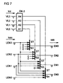
- FIG. 5 and FIG. 6 together show the module selection unit MAE - see FIG. 2.
- the two address lines ADL0.1, ADL2.3 are each decoded on four output lines A1..4, each assigned to an insertion area EB1..4.
- the output lines A1..4 of the second decoding unit DK-4 are each connected to an input of four AND gates & (1..4).
- the second to fourth output lines A2..4 are each additionally connected to an input of fifth to seventh AND gates & (5..7).
- the four output lines A1..4 of the first decoding unit DK-1 are routed to a first shift stage S1 and in each of these are connected to an input of two multiplex elements MX.
- the still free input of the fourth multiplex element MX is coupled to zero potential 0.
- the output of the least significant multiplex element MX is connected to an input of an eighth AND gate & (8) and the outputs of the three further multiplex elements MX are each connected to an input of multiplex elements MX of a second shift stage S2.
- the output of the least significant multiplex element MX is routed with a ninth AND gate & (9) and the outputs of the two remaining multiplex elements MX each with an input of two further multiplex elements MX forming a third shift stage S3.
- the output of the lower-order multiplex element MX is connected to the input of a tenth AND gate & (10) and the output of the remaining multiplex element MX connected to an input of an eleventh AND gate & (11).
- the further input of the fourth AND gate & (4) is connected to the fourth K4 line K4 (3) and a further input of the third AND gate & (3) is connected to the further input of the seventh AND gate & (7) , the third K4 line K4 (2) and connected to the control input ST of the third shift stage S3.
- a further input of the second AND gate & (2) is routed to a further input of the sixth AND gate & (6), to the second K4 line K4 (1) and to the control input ST of the second shift stage S2.
- Another input of the first AND gate & (1) has a connection to a further input of the fifth AND gate & (5), the first K4 line K4 (0) and a control input ST of the first shift stage S1.
- the outputs of the fifth to seventh AND gates & (5..7) are combined in a first OR gate OD1, the output of which is connected to an enable input EN of the first decoding unit DK-1.
- the outputs of the first to fourth AND gates & (1..4) are coupled to a second OR gate OD2, the inverting output of which is connected to a further input of the eighth to eleventh AND gates & (8..11) .
- a binary information is present at the outputs EN4 (0..3) of the four AND gates & (1..4), which indicates whether a memory module SM is also present for the address information AD0.1 currently occurring on the address lines ADL0.1 the capacity K4 is available in one of the four application areas EB1..4.
- the outputs EN1 (0..3) of the eighth to eleventh AND gates & (8..11) there is also logical information as to whether a memory module SM is present in the address information AD2.3 currently present on the address lines ADL2.3 small capacity K1 is available in one of the four application areas EB1..4.
- Figure 6 shows four OR gates OD (1..4), at one input of which the respective output EN4 (0..3) of the first to fourth AND gate & (1..4) - see Figure 5 - and at their other input an output EN1 (0..3) of the eighth to eleventh AND gate & (8..11) is carried.
- the outputs of the four OR gates OD1 (1..4) are each connected to an input of four AND gates & (1..4).
- One of the four logical introductions LVL0..3 is routed to the other inputs of the four AND gates & (1..4).
- the logic memory drive signal lsas is now present at the outputs LEN0..3 of the four AND gates & (1..4).
- This logic memory control signal lsas shows in binary form which application area EB1..4 is to be controlled logically.
- the conversion of the logic memory drive signal lsas into the physical memory drive signal sas is shown in FIG.
- the four introductions VL0..3 - see FIG. 3 - are routed to a third decoding unit DK-3.
- the four outputs A1..A4 of the third decoding unit DK-3 are each connected to a control input ST of four shift stages S1..4.
- the sliding stages S1..4 are implemented in the same way as shown in FIG. 3 or 5.
- a decoding table is stored, by means of which the shift stages S1..4 are controlled in this way be that the memory control signal sas is present in binary form at the four outputs EN0..3 of the four shift stages S1..4, each output EN0..3 being separately connected to an insertion range EB1..4.
- the sub-memory area in the released memory module SM is controlled and data transmitted by the microprocessor MP is stored or data is read and transmitted to the microprocessor MP.
- the memory module SM used in the third application area EB3 is released, that is, addressed.
Landscapes
- Engineering & Computer Science (AREA)
- Theoretical Computer Science (AREA)
- Physics & Mathematics (AREA)
- General Engineering & Computer Science (AREA)
- General Physics & Mathematics (AREA)
- Memory System (AREA)
- Static Random-Access Memory (AREA)
- Image Input (AREA)
Applications Claiming Priority (2)
| Application Number | Priority Date | Filing Date | Title |
|---|---|---|---|
| DE19549061 | 1995-12-29 | ||
| DE19549061 | 1995-12-29 |
Publications (2)
| Publication Number | Publication Date |
|---|---|
| EP0782077A1 true EP0782077A1 (fr) | 1997-07-02 |
| EP0782077B1 EP0782077B1 (fr) | 2003-08-20 |
Family
ID=7781601
Family Applications (1)
| Application Number | Title | Priority Date | Filing Date |
|---|---|---|---|
| EP96119487A Expired - Lifetime EP0782077B1 (fr) | 1995-12-29 | 1996-12-04 | Procédé et arrangement pour convertir des adresses de mémoire en signaux de commande de mémoire |
Country Status (5)
| Country | Link |
|---|---|
| US (1) | US6003110A (fr) |
| EP (1) | EP0782077B1 (fr) |
| JP (1) | JP3266529B2 (fr) |
| DE (1) | DE59610672D1 (fr) |
| SG (1) | SG46760A1 (fr) |
Cited By (1)
| Publication number | Priority date | Publication date | Assignee | Title |
|---|---|---|---|---|
| GB2357602A (en) * | 1999-12-22 | 2001-06-27 | Nokia Mobile Phones Ltd | Memory controller for a memory array comprising different memory types |
Families Citing this family (5)
| Publication number | Priority date | Publication date | Assignee | Title |
|---|---|---|---|---|
| JPH09293015A (ja) * | 1996-04-24 | 1997-11-11 | Mitsubishi Electric Corp | メモリシステムおよびそれに用いられる半導体記憶装置 |
| JP3365283B2 (ja) * | 1997-11-14 | 2003-01-08 | 日本電気株式会社 | 半導体記憶装置 |
| JP3498021B2 (ja) | 1999-10-07 | 2004-02-16 | エヌイーシーコンピュータテクノ株式会社 | メモリ制御方式 |
| US7339837B2 (en) * | 2004-05-18 | 2008-03-04 | Infineon Technologies Ag | Configurable embedded processor |
| US7308527B2 (en) * | 2005-01-24 | 2007-12-11 | International Business Machines Corporation | System for indicating a plug position for a memory module in a memory system |
Citations (2)
| Publication number | Priority date | Publication date | Assignee | Title |
|---|---|---|---|---|
| EP0285986A2 (fr) * | 1987-04-01 | 1988-10-12 | International Business Machines Corporation | Système de traitement de données avec moyens d'adressage en contigu d'une mémoire |
| EP0289899A2 (fr) * | 1987-05-04 | 1988-11-09 | Prime Computer, Inc. | Système de commande de mémoire |
Family Cites Families (5)
| Publication number | Priority date | Publication date | Assignee | Title |
|---|---|---|---|---|
| US5119486A (en) * | 1989-01-17 | 1992-06-02 | Prime Computer | Memory board selection method and apparatus |
| JPH0715665B2 (ja) * | 1991-06-10 | 1995-02-22 | インターナショナル・ビジネス・マシーンズ・コーポレイション | パーソナルコンピユータ |
| DE59206051D1 (de) * | 1992-02-28 | 1996-05-23 | Siemens Ag | Verfahren zur hierarchisch administrierbaren kennungsorientierten Freigabesteuerung für bedieneraufgabenbezogene Zugriffsanweisungen auf eine Datenbasis einer programmgesteuerten Kommunikationsanlage |
| US5446860A (en) * | 1993-01-11 | 1995-08-29 | Hewlett-Packard Company | Apparatus for determining a computer memory configuration of memory modules using presence detect bits shifted serially into a configuration register |
| EP0629952B1 (fr) * | 1993-06-16 | 1999-09-01 | Bull HN Information Systems Italia S.p.A. | Mémoire avec niveau d'entrelacement variable et unité de configuration apparentée |
-
1996
- 1996-12-04 DE DE59610672T patent/DE59610672D1/de not_active Expired - Lifetime
- 1996-12-04 EP EP96119487A patent/EP0782077B1/fr not_active Expired - Lifetime
- 1996-12-10 SG SG1996011616A patent/SG46760A1/en unknown
- 1996-12-25 JP JP34590196A patent/JP3266529B2/ja not_active Expired - Fee Related
- 1996-12-30 US US08/774,459 patent/US6003110A/en not_active Expired - Lifetime
Patent Citations (2)
| Publication number | Priority date | Publication date | Assignee | Title |
|---|---|---|---|---|
| EP0285986A2 (fr) * | 1987-04-01 | 1988-10-12 | International Business Machines Corporation | Système de traitement de données avec moyens d'adressage en contigu d'une mémoire |
| EP0289899A2 (fr) * | 1987-05-04 | 1988-11-09 | Prime Computer, Inc. | Système de commande de mémoire |
Non-Patent Citations (1)
| Title |
|---|
| "DYNAMIC SELF-CONFIGURATION FOR MEMEORY CARDS ARRANGEMENT", IBM TECHNICAL DISCLOSURE BULLETIN, vol. 31, no. 12, 1 May 1989 (1989-05-01), pages 213 - 216, XP000110911 * |
Cited By (2)
| Publication number | Priority date | Publication date | Assignee | Title |
|---|---|---|---|---|
| GB2357602A (en) * | 1999-12-22 | 2001-06-27 | Nokia Mobile Phones Ltd | Memory controller for a memory array comprising different memory types |
| US6563739B2 (en) | 1999-12-22 | 2003-05-13 | Nokia Mobile Phones Limited | System and method for transferring data between different types of memory using a common data bus |
Also Published As
| Publication number | Publication date |
|---|---|
| EP0782077B1 (fr) | 2003-08-20 |
| US6003110A (en) | 1999-12-14 |
| SG46760A1 (en) | 1998-02-20 |
| JPH09212413A (ja) | 1997-08-15 |
| JP3266529B2 (ja) | 2002-03-18 |
| DE59610672D1 (de) | 2003-09-25 |
Similar Documents
| Publication | Publication Date | Title |
|---|---|---|
| DE2803989C2 (de) | Digitaldatenspeicher mit wahlfreiem Zugriff | |
| DE3015875A1 (de) | Speicherzugriffssystem und verfahren fuer einen zugriff zu einem digitalen speichersystem | |
| DE3618136C2 (fr) | ||
| DE3043100C2 (fr) | ||
| DE2926322C2 (de) | Speicher-Subsystem | |
| DE2527062C3 (de) | Anpassungsfähiger Adressendecodierer | |
| DE2364253A1 (de) | Schaltungsanordnung fuer mikroprogrammierte geraete der datenverarbeitung | |
| DE2213953C3 (de) | Schaltungsanordnung zum Darstellen von Zeichen auf dem Bildschirm eines Sichtgerätes | |
| EP0782077A1 (fr) | Procédé et arrangement pour convertir des adresses de mémoire en signaux de commande de mémoire | |
| DE3526521C2 (fr) | ||
| DE3024153A1 (de) | Speicher-subsystem | |
| DE1234054B (de) | Byte-Umsetzer | |
| DE10036643A1 (de) | Verfahren und Vorrichtung zur Steuerung von Betriebsabläufen | |
| DE2365778A1 (de) | Rechner | |
| DE2233164A1 (de) | Schaltungsanordnung zur ausblendung eines beliebig waehlbaren bereichs einer bitfolge bei deren uebertragung zwischen zwei registern | |
| EP0494329B1 (fr) | Circuit électrique pour le mappage de l'espace d'adressage logique d'une unité de traitement vers l'espace d'adressage physique d'une mémoire | |
| DE3105503A1 (de) | Assoziativer zugriffsspeicher | |
| EP0880092B1 (fr) | Dispositif à commande programmée avec possibilité de chargement et de mise en opération d'un deuxième système d'exploitation, sans interruption de l'exécution du dispositif | |
| DE3149905A1 (de) | Elektronisches geraet | |
| DE1499284B2 (de) | Datenverarbeitungsanlage | |
| DE2017879B2 (de) | Speicheranordnung mit freiem Zugriff | |
| DE3331043C2 (fr) | ||
| DE10208073A1 (de) | Treiberschaltung für eine LCD-Anzeige | |
| EP0480331A2 (fr) | Système de traitement de données avec terminaux d'affichage | |
| DE3538452A1 (de) | Verfahren und anordnung zum meiden defekter abschnitte in speicherfeldern und verfahren zum adressieren solcher speicherfelder |
Legal Events
| Date | Code | Title | Description |
|---|---|---|---|
| PUAI | Public reference made under article 153(3) epc to a published international application that has entered the european phase |
Free format text: ORIGINAL CODE: 0009012 |
|
| AK | Designated contracting states |
Kind code of ref document: A1 Designated state(s): DE FR GB IT NL |
|
| 17P | Request for examination filed |
Effective date: 19970721 |
|
| 17Q | First examination report despatched |
Effective date: 20010730 |
|
| GRAH | Despatch of communication of intention to grant a patent |
Free format text: ORIGINAL CODE: EPIDOS IGRA |
|
| GRAS | Grant fee paid |
Free format text: ORIGINAL CODE: EPIDOSNIGR3 |
|
| GRAA | (expected) grant |
Free format text: ORIGINAL CODE: 0009210 |
|
| AK | Designated contracting states |
Designated state(s): DE FR GB IT NL |
|
| PG25 | Lapsed in a contracting state [announced via postgrant information from national office to epo] |
Ref country code: NL Free format text: LAPSE BECAUSE OF FAILURE TO SUBMIT A TRANSLATION OF THE DESCRIPTION OR TO PAY THE FEE WITHIN THE PRESCRIBED TIME-LIMIT Effective date: 20030820 |
|
| REG | Reference to a national code |
Ref country code: GB Ref legal event code: FG4D Free format text: NOT ENGLISH |
|
| REF | Corresponds to: |
Ref document number: 59610672 Country of ref document: DE Date of ref document: 20030925 Kind code of ref document: P |
|
| GBT | Gb: translation of ep patent filed (gb section 77(6)(a)/1977) | ||
| NLV1 | Nl: lapsed or annulled due to failure to fulfill the requirements of art. 29p and 29m of the patents act | ||
| ET | Fr: translation filed | ||
| PLBE | No opposition filed within time limit |
Free format text: ORIGINAL CODE: 0009261 |
|
| STAA | Information on the status of an ep patent application or granted ep patent |
Free format text: STATUS: NO OPPOSITION FILED WITHIN TIME LIMIT |
|
| REG | Reference to a national code |
Ref country code: HK Ref legal event code: WD Ref document number: 1000843 Country of ref document: HK |
|
| 26N | No opposition filed |
Effective date: 20040524 |
|
| REG | Reference to a national code |
Ref country code: GB Ref legal event code: 732E Free format text: REGISTERED BETWEEN 20121025 AND 20121031 |
|
| REG | Reference to a national code |
Ref country code: FR Ref legal event code: TP Owner name: SIEMENS ENTERPRISE COMMUNICATIONS GMBH & CO. K, DE Effective date: 20130108 |
|
| REG | Reference to a national code |
Ref country code: DE Ref legal event code: R082 Ref document number: 59610672 Country of ref document: DE Representative=s name: FRITZSCHE PATENT, DE |
|
| REG | Reference to a national code |
Ref country code: DE Ref legal event code: R082 Ref document number: 59610672 Country of ref document: DE Representative=s name: FRITZSCHE PATENTANWAELTE, DE Effective date: 20130313 Ref country code: DE Ref legal event code: R082 Ref document number: 59610672 Country of ref document: DE Representative=s name: FRITZSCHE PATENT, DE Effective date: 20130313 Ref country code: DE Ref legal event code: R081 Ref document number: 59610672 Country of ref document: DE Owner name: UNIFY GMBH & CO. KG, DE Free format text: FORMER OWNER: SIEMENS AKTIENGESELLSCHAFT, 80333 MUENCHEN, DE Effective date: 20130313 Ref country code: DE Ref legal event code: R081 Ref document number: 59610672 Country of ref document: DE Owner name: SIEMENS ENTERPRISE COMMUNICATIONS GMBH & CO. K, DE Free format text: FORMER OWNER: SIEMENS AKTIENGESELLSCHAFT, 80333 MUENCHEN, DE Effective date: 20130313 |
|
| REG | Reference to a national code |
Ref country code: DE Ref legal event code: R082 Ref document number: 59610672 Country of ref document: DE Representative=s name: FRITZSCHE PATENT, DE |
|
| REG | Reference to a national code |
Ref country code: DE Ref legal event code: R082 Ref document number: 59610672 Country of ref document: DE Representative=s name: FRITZSCHE PATENTANWAELTE, DE Effective date: 20131112 Ref country code: DE Ref legal event code: R082 Ref document number: 59610672 Country of ref document: DE Representative=s name: FRITZSCHE PATENT, DE Effective date: 20131112 Ref country code: DE Ref legal event code: R081 Ref document number: 59610672 Country of ref document: DE Owner name: UNIFY GMBH & CO. KG, DE Free format text: FORMER OWNER: SIEMENS ENTERPRISE COMMUNICATIONS GMBH & CO. KG, 81379 MUENCHEN, DE Effective date: 20131112 |
|
| REG | Reference to a national code |
Ref country code: FR Ref legal event code: CD Owner name: UNIFY GMBH & CO.KG, DE Effective date: 20140429 |
|
| PGFP | Annual fee paid to national office [announced via postgrant information from national office to epo] |
Ref country code: GB Payment date: 20141216 Year of fee payment: 19 |
|
| PGFP | Annual fee paid to national office [announced via postgrant information from national office to epo] |
Ref country code: FR Payment date: 20141212 Year of fee payment: 19 |
|
| PGFP | Annual fee paid to national office [announced via postgrant information from national office to epo] |
Ref country code: IT Payment date: 20141218 Year of fee payment: 19 |
|
| PGFP | Annual fee paid to national office [announced via postgrant information from national office to epo] |
Ref country code: DE Payment date: 20151217 Year of fee payment: 20 |
|
| GBPC | Gb: european patent ceased through non-payment of renewal fee |
Effective date: 20151204 |
|
| REG | Reference to a national code |
Ref country code: DE Ref legal event code: R082 Ref document number: 59610672 Country of ref document: DE Representative=s name: FRITZSCHE PATENTANWAELTE, DE Ref country code: DE Ref legal event code: R081 Ref document number: 59610672 Country of ref document: DE Owner name: UNIFY GMBH & CO. KG, DE Free format text: FORMER OWNER: UNIFY GMBH & CO. KG, 81379 MUENCHEN, DE |
|
| REG | Reference to a national code |
Ref country code: FR Ref legal event code: ST Effective date: 20160831 |
|
| PG25 | Lapsed in a contracting state [announced via postgrant information from national office to epo] |
Ref country code: GB Free format text: LAPSE BECAUSE OF NON-PAYMENT OF DUE FEES Effective date: 20151204 |
|
| PG25 | Lapsed in a contracting state [announced via postgrant information from national office to epo] |
Ref country code: FR Free format text: LAPSE BECAUSE OF NON-PAYMENT OF DUE FEES Effective date: 20151231 |
|
| REG | Reference to a national code |
Ref country code: DE Ref legal event code: R071 Ref document number: 59610672 Country of ref document: DE |
|
| PG25 | Lapsed in a contracting state [announced via postgrant information from national office to epo] |
Ref country code: IT Free format text: LAPSE BECAUSE OF NON-PAYMENT OF DUE FEES Effective date: 20151204 |