EP0773689A1 - Videodatenverabeitungsvorrichtung mit Pufferspeicher - Google Patents
Videodatenverabeitungsvorrichtung mit Pufferspeicher Download PDFInfo
- Publication number
- EP0773689A1 EP0773689A1 EP96402376A EP96402376A EP0773689A1 EP 0773689 A1 EP0773689 A1 EP 0773689A1 EP 96402376 A EP96402376 A EP 96402376A EP 96402376 A EP96402376 A EP 96402376A EP 0773689 A1 EP0773689 A1 EP 0773689A1
- Authority
- EP
- European Patent Office
- Prior art keywords
- buffer memory
- packet
- data
- circuit
- pointer
- Prior art date
- Legal status (The legal status is an assumption and is not a legal conclusion. Google has not performed a legal analysis and makes no representation as to the accuracy of the status listed.)
- Granted
Links
Images
Classifications
-
- H—ELECTRICITY
- H04—ELECTRIC COMMUNICATION TECHNIQUE
- H04N—PICTORIAL COMMUNICATION, e.g. TELEVISION
- H04N19/00—Methods or arrangements for coding, decoding, compressing or decompressing digital video signals
- H04N19/10—Methods or arrangements for coding, decoding, compressing or decompressing digital video signals using adaptive coding
- H04N19/134—Methods or arrangements for coding, decoding, compressing or decompressing digital video signals using adaptive coding characterised by the element, parameter or criterion affecting or controlling the adaptive coding
- H04N19/146—Data rate or code amount at the encoder output
- H04N19/152—Data rate or code amount at the encoder output by measuring the fullness of the transmission buffer
-
- H—ELECTRICITY
- H04—ELECTRIC COMMUNICATION TECHNIQUE
- H04N—PICTORIAL COMMUNICATION, e.g. TELEVISION
- H04N19/00—Methods or arrangements for coding, decoding, compressing or decompressing digital video signals
- H04N19/50—Methods or arrangements for coding, decoding, compressing or decompressing digital video signals using predictive coding
Definitions
- the invention relates to a data processing device comprising a buffer memory in order to allow circuits having access to this memory to work at different speeds.
- the invention is particularly applicable in a digital packet data transmission system such as a digital television transmission and reception system such as DVB ("Digital Video Broadcast").
- a digital television receiver comprises a reception and demodulation part and a part for processing the information proper.
- the data at the output of the reception part is generally in the form of binary word packets of given length.
- the information processing part does not necessarily process the data packets at the same speed as they are transmitted from the reception part: the processing speed can be much higher than the reception speed.
- a buffer memory is then inserted between the two parts which decouples the writing by the receiving part and the reading by the processing part, each of the two parts working asynchronously.
- the means for resetting said pointer to zero comprise a comparator which compares a packet start synchronization word with the data received.
- the device comprises means for resetting the second circuit when the reading in said buffer memory has not started for a determined time interval after the start of writing a data packet in said buffer.
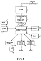
- Figure 1 shows a block diagram of a digital satellite television receiver.
- FIG. 2 illustrates the memory in accordance with the exemplary embodiment with respect to the size of a data packet.
- FIG. 1 shows a block diagram of a digital television decoder.
- This decoder has a tuner 1 connected to a low noise frequency converter which converts the signals received by a satellite dish.
- the tuner makes it possible to obtain a signal modulated in baseband, which will be demodulated and corrected by a demodulator-corrector of errors 2.
- the correction of errors is of Reed-Solomon type according to the present example.
- the digital signal is available at the output of block 2.
- the data stream transported by this signal comprises data packets called transport packets, having a fixed length of 188 bytes.
- the organization of the packets is described in the ISO / IEC 13818-1 to ISO / IEC 13818-3 standards, commonly known as MPEG II. Systems, Video and Audio. We will consider for example in this context appendix F of MPEG II Systems, which shows the types and lengths of the data fields in the different packets.
- the demodulator and error corrector 2 writes to a synchronization memory 3, which has the structure of a FIFO stack.
- the data processing part (references 4 and following) reads data from memory at its own pace.
- a demultiplexer circuit 4 has filters intended to signal the presence of certain types of predetermined data in the received packets.
- the types of data for example audio, video, access control data, etc., are identified by identification words, compared by the filters to a certain number of predetermined words. Depending on the filtering result, the packets or pieces of packets are then routed to the appropriate application decoders.
- the demultiplexer 4 is controlled by a microcontroller 5 which on the one hand writes to the internal registers of the demultiplexer and manages a RAM memory 6 containing in particular the reprogrammable filters.
- the demultiplexer 4 addresses this RAM memory as a function of the binary words to be filtered and reads there the result of a filtering. Such filtering is described in more detail in French patent application FR 95 02348.
- the application decoders include an MPEG II video decoder 8 and an MPEG II audio decoder 9, implemented for example with integrated circuits manufactured by SGS Thomson.
- An interface 10 for a smart card 11 is also connected to the demultiplexer 4, which transmits to the smart card access control management data linked to the specific address of this card, as well as authorization messages from the card of which determines the control words necessary for descrambling the transmissions.
- the communication protocol between the interface 10 and the card 11 conforms to the ISO 7816-3 standard.
- a "Teletext" reinsertion circuit 12 reinserts the teletext data transmitted in separate packets from the video data into the video signal.
- the "Teletext" circuit is a circuit such as that described in French patent application FR 94 08195.
- the demultiplexer shares with the application decoders, the smart card interface and the "Teletext" circuit the resources of a RAM 7. Buffers are allocated to the different circuits. The demultiplexer temporarily stores data which is subsequently read back by these circuits.
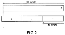
- the MPEG II System transport packet is 188 bytes long.
- the choice of the size of the FIFO 3 memory depends on this value. In fact, it is sought to use a FIFO the size of which is less than the size of an entire packet, for the purpose of economy.
- FIFO memory 3 is managed by a write address pointer and a read address pointer. When the pointers reach the end of memory, they are automatically reset to zero. As regards the present exemplary embodiment, the pointers are an integral part of the memory 3.
- the size of the memory is chosen according to the following constraint: when the end of a packet is written to a given address, the distance between this address and the address from which the next packet will be written must be maximum. This makes it possible to maximize the time available to the demultiplexer 4 for reading the data in this memory before it is erased by writing the next packet.
- the memory size is 63 bytes. This corresponds to a third of the size of the data packet, rounded up to the nearest integer, since the size of the packet divided by three does not give an integer.
- FIG. 2 illustrates the method of writing a typical packet, that is to say a packet written without interruption, in memory 3.
- the writing of a packet begins at a fixed address, by convention address 0.
- the write pointer is reset to zero when the demodulator and corrector circuit 2 sends a data validation signal whose rising edge signals the start of a transport packet or after an interruption in the operation of the system.
- the validation signal is also transmitted to components of the demultiplexer to inform it that a packet can be read.
- the first pass (digit 1), the first 63 bytes of the packet are written, the write pointer looping back to address 0 at the end of memory. Similarly, the next 63 bytes are written on the second pass. During the third pass, the end of the packet is written to the penultimate address in memory, leaving one byte free before the write counter is reset to zero for writing the next packet.
- the distance between the last byte of a packet and the first byte of the following packet is optimized.
- the read pointer is reset to zero at the end of the packet or after a system interruption (erroneous data, power failure, etc.), since the start address of the next packet is fixed at address 0.
- a reset signal of the demultiplexer is generated when the latter has not started to read the buffer memory a certain number of clock cycles after the start of writing a packet.
- This signal forces the demultiplexer to start processing the packet in progress, the reinitialization having the effect of bringing the demultiplexer out of a possible abnormal state.
- This variant makes it possible to obtain rapid synchronization on a demultiplexer on the data written in the buffer memory. Indeed, the data validation signal transmitted by circuit 2 to circuit 4 only informs the latter of the presence of a new packet, without however forcing it to consider this new packet immediately. This allows circuit 4 if necessary to finish processing the previous packet.
- the reset signal is generated when the first 58 bytes of a packet have been written without the reader having started.
- the present invention is not limited to the numerical values given in the description of the exemplary embodiment.
- the division factor used to determine the size of the memory relative to the size of a data packet can be different from 3. In this case, depending on whether this factor is or not a packet size divider, rounding up may not be necessary.
Applications Claiming Priority (2)
| Application Number | Priority Date | Filing Date | Title |
|---|---|---|---|
| FR9513281A FR2741172B1 (fr) | 1995-11-09 | 1995-11-09 | Dispositif de traitement de donnees comportant une memoire tampon |
| FR9513281 | 1995-11-09 |
Publications (2)
| Publication Number | Publication Date |
|---|---|
| EP0773689A1 true EP0773689A1 (de) | 1997-05-14 |
| EP0773689B1 EP0773689B1 (de) | 2002-05-02 |
Family
ID=9484403
Family Applications (1)
| Application Number | Title | Priority Date | Filing Date |
|---|---|---|---|
| EP19960402376 Expired - Lifetime EP0773689B1 (de) | 1995-11-09 | 1996-11-07 | Videodatenverabeitungsvorrichtung mit Pufferspeicher |
Country Status (5)
| Country | Link |
|---|---|
| EP (1) | EP0773689B1 (de) |
| JP (1) | JP3734578B2 (de) |
| CN (1) | CN1110160C (de) |
| DE (1) | DE69620978T2 (de) |
| FR (1) | FR2741172B1 (de) |
Cited By (2)
| Publication number | Priority date | Publication date | Assignee | Title |
|---|---|---|---|---|
| CN100366022C (zh) * | 2004-04-02 | 2008-01-30 | 华为技术有限公司 | 一种缓存分配方法及装置 |
| CN101309261B (zh) * | 2008-07-14 | 2011-04-06 | 成都卫士通信息产业股份有限公司 | 一种网络数据报文处理方法及系统、设备 |
Families Citing this family (4)
| Publication number | Priority date | Publication date | Assignee | Title |
|---|---|---|---|---|
| EP0946053A1 (de) * | 1998-03-27 | 1999-09-29 | CANAL+ Société Anonyme | Speicherverwaltung in einem Empfänger/Decoder |
| JP2004171411A (ja) * | 2002-11-21 | 2004-06-17 | Hitachi Global Storage Technologies Netherlands Bv | データ記憶装置及びバッファメモリの管理方法 |
| CN102023821A (zh) * | 2010-12-16 | 2011-04-20 | 成都市华为赛门铁克科技有限公司 | 一种磁盘空间管理方法及系统 |
| CN103491426A (zh) * | 2013-08-31 | 2014-01-01 | 中山大学 | 一种iptv的视频点播系统 |
Citations (4)
| Publication number | Priority date | Publication date | Assignee | Title |
|---|---|---|---|---|
| JPS62177647A (ja) * | 1986-01-31 | 1987-08-04 | Toshiba Corp | 通信制御装置におけるバツフア管理方式 |
| EP0309280A1 (de) * | 1987-09-23 | 1989-03-29 | BRITISH TELECOMMUNICATIONS public limited company | Videokoder |
| EP0430051A2 (de) * | 1989-12-01 | 1991-06-05 | National Semiconductor Corporation | Bytebreite elastische Puffereinrichtung |
| EP0598346A2 (de) * | 1992-11-19 | 1994-05-25 | General Instrument Corporation Of Delaware | Doppelpufferschema für Dekodierer variabler Länge |
-
1995
- 1995-11-09 FR FR9513281A patent/FR2741172B1/fr not_active Expired - Fee Related
-
1996
- 1996-11-07 JP JP29552096A patent/JP3734578B2/ja not_active Expired - Fee Related
- 1996-11-07 DE DE1996620978 patent/DE69620978T2/de not_active Expired - Lifetime
- 1996-11-07 EP EP19960402376 patent/EP0773689B1/de not_active Expired - Lifetime
- 1996-11-09 CN CN96121933A patent/CN1110160C/zh not_active Expired - Lifetime
Patent Citations (4)
| Publication number | Priority date | Publication date | Assignee | Title |
|---|---|---|---|---|
| JPS62177647A (ja) * | 1986-01-31 | 1987-08-04 | Toshiba Corp | 通信制御装置におけるバツフア管理方式 |
| EP0309280A1 (de) * | 1987-09-23 | 1989-03-29 | BRITISH TELECOMMUNICATIONS public limited company | Videokoder |
| EP0430051A2 (de) * | 1989-12-01 | 1991-06-05 | National Semiconductor Corporation | Bytebreite elastische Puffereinrichtung |
| EP0598346A2 (de) * | 1992-11-19 | 1994-05-25 | General Instrument Corporation Of Delaware | Doppelpufferschema für Dekodierer variabler Länge |
Non-Patent Citations (3)
| Title |
|---|
| ISO 7816-3: "Le protocole de communication entre l'interface 10 et la carte 11" |
| ISO/IEC 13818-1 À ISO/IEC 13818-3: "MPEG II Systèmes, Vidéo et Audio" |
| PATENT ABSTRACTS OF JAPAN vol. 12, no. 23 (P - 658) 23 January 1988 (1988-01-23) * |
Cited By (2)
| Publication number | Priority date | Publication date | Assignee | Title |
|---|---|---|---|---|
| CN100366022C (zh) * | 2004-04-02 | 2008-01-30 | 华为技术有限公司 | 一种缓存分配方法及装置 |
| CN101309261B (zh) * | 2008-07-14 | 2011-04-06 | 成都卫士通信息产业股份有限公司 | 一种网络数据报文处理方法及系统、设备 |
Also Published As
| Publication number | Publication date |
|---|---|
| JP3734578B2 (ja) | 2006-01-11 |
| FR2741172A1 (fr) | 1997-05-16 |
| CN1152244A (zh) | 1997-06-18 |
| DE69620978T2 (de) | 2002-10-31 |
| CN1110160C (zh) | 2003-05-28 |
| FR2741172B1 (fr) | 1997-12-12 |
| JPH09261279A (ja) | 1997-10-03 |
| DE69620978D1 (de) | 2002-06-06 |
| EP0773689B1 (de) | 2002-05-02 |
Similar Documents
| Publication | Publication Date | Title |
|---|---|---|
| EP0426923B1 (de) | Verfahren und Vorrichtung zur Verschleierung und Entschleierung zusammengesetzter Videosignale | |
| EP0078185B1 (de) | Rundfunk-Datenpakete-Empfänger | |
| FR2525420A1 (fr) | Systeme de transmission de donnees sur un reseau de cables | |
| EP0113307A1 (de) | Anpassungseinrichtung für digitale Informationsblöcke fester Länge | |
| FR2500249A1 (de) | ||
| EP0019545A1 (de) | Mit Mitteln zum Schutz gegen Übertragungsfehler versehenes Videotextsystem | |
| EP0328440A1 (de) | Selektionssystem zum Empfang von Radio- oder Fernsehübertragungen | |
| EP0268481A2 (de) | Verfahren zum Aufzeichnen von synchronisierter Audio- und Videoinformation | |
| EP0773689B1 (de) | Videodatenverabeitungsvorrichtung mit Pufferspeicher | |
| EP0238382B1 (de) | Vorrichtung zum Demultiplexieren von Datenpaketen eines Funkübertragungssignals nach der MAC-Paketennorm | |
| EP0772361B1 (de) | Verfahren zur Hintereinanderschaltung von austauschbaren, bedingungsabhängigen Zugangsmodulen, Schaltung zur Eingabe einer vorbestimmten Reihenfolge und Schaltung zur Erkennung dieser Reihenfolge zum Starten dieses Verfahrens | |
| US4908812A (en) | Synchronizing signal reproducing circuit in a disc playback device | |
| EP1217831B1 (de) | Verfahren und Anordnung zur Filterung von Daten bezüglich einer elektronischen Programmübersicht für Fernseher | |
| EP0097579A1 (de) | Funkverbindungssystem nach dem Frequenzsprungverfahren mit Redundanz zwischen den einzelnen Frequenzstufen | |
| FR2643766A1 (fr) | Circuit pour former une information de synchronisation a partir d'un signal video numerique | |
| EP0130899A2 (de) | Programmierbare Serien-/Parallelumsetzerschaltung für ein digitales Signal und ihre Anwendung in einem Empfänger für digitale Videosignale | |
| US7522223B2 (en) | Audio signal delay apparatus and method | |
| EP0341166A1 (de) | Verfahren und Vorrichtung zur asynchronen Übertragung von Datenpaketen | |
| EP1112658B1 (de) | Dekoder für ein system mit bedingtem zugang und verfahren zum laden von benutzerrechten in einem solchen system | |
| EP0044780B1 (de) | Digitales Kommunikationssystem auf einem Kanal mit kontinuierlichem Datenfluss | |
| EP0148098A2 (de) | Schaltung zur Regeneration von periodischen Signalen | |
| JP3194281B2 (ja) | 光空間伝送システム | |
| FR2780228A1 (fr) | Dispositif de transmission d'informations audio et video | |
| WO2000030017A1 (fr) | Procede de transmission numerique | |
| EP0517556B1 (de) | Verfahren zur Demodulation von RDS-Signalen auf numerische Weise, und Demodulator zur Durchführung dieses Verfahrens |
Legal Events
| Date | Code | Title | Description |
|---|---|---|---|
| PUAI | Public reference made under article 153(3) epc to a published international application that has entered the european phase |
Free format text: ORIGINAL CODE: 0009012 |
|
| AK | Designated contracting states |
Kind code of ref document: A1 Designated state(s): DE FR GB IT |
|
| 17P | Request for examination filed |
Effective date: 19970912 |
|
| RAP1 | Party data changed (applicant data changed or rights of an application transferred) |
Owner name: THOMSON MULTIMEDIA |
|
| 17Q | First examination report despatched |
Effective date: 19991026 |
|
| GRAG | Despatch of communication of intention to grant |
Free format text: ORIGINAL CODE: EPIDOS AGRA |
|
| GRAG | Despatch of communication of intention to grant |
Free format text: ORIGINAL CODE: EPIDOS AGRA |
|
| GRAH | Despatch of communication of intention to grant a patent |
Free format text: ORIGINAL CODE: EPIDOS IGRA |
|
| REG | Reference to a national code |
Ref country code: GB Ref legal event code: IF02 |
|
| GRAH | Despatch of communication of intention to grant a patent |
Free format text: ORIGINAL CODE: EPIDOS IGRA |
|
| GRAA | (expected) grant |
Free format text: ORIGINAL CODE: 0009210 |
|
| AK | Designated contracting states |
Kind code of ref document: B1 Designated state(s): DE FR GB IT |
|
| REG | Reference to a national code |
Ref country code: GB Ref legal event code: FG4D Free format text: NOT ENGLISH |
|
| REF | Corresponds to: |
Ref document number: 69620978 Country of ref document: DE Date of ref document: 20020606 |
|
| GBT | Gb: translation of ep patent filed (gb section 77(6)(a)/1977) |
Effective date: 20020719 |
|
| PLBE | No opposition filed within time limit |
Free format text: ORIGINAL CODE: 0009261 |
|
| STAA | Information on the status of an ep patent application or granted ep patent |
Free format text: STATUS: NO OPPOSITION FILED WITHIN TIME LIMIT |
|
| 26N | No opposition filed |
Effective date: 20030204 |
|
| REG | Reference to a national code |
Ref country code: DE Ref legal event code: R082 Ref document number: 69620978 Country of ref document: DE Representative=s name: MANFRED ROSSMANITH, DE |
|
| REG | Reference to a national code |
Ref country code: DE Ref legal event code: R084 Ref document number: 69620978 Country of ref document: DE Effective date: 20111116 |
|
| REG | Reference to a national code |
Ref country code: DE Ref legal event code: R082 Ref document number: 69620978 Country of ref document: DE Representative=s name: ROSSMANITH, MANFRED, DIPL.-PHYS. DR.RER.NAT., DE Effective date: 20120111 Ref country code: DE Ref legal event code: R081 Ref document number: 69620978 Country of ref document: DE Owner name: THOMSON LICENSING, FR Free format text: FORMER OWNER: THOMSON MULTIMEDIA, BOULOGNE, FR Effective date: 20120111 |
|
| PGFP | Annual fee paid to national office [announced via postgrant information from national office to epo] |
Ref country code: GB Payment date: 20141121 Year of fee payment: 19 Ref country code: DE Payment date: 20141120 Year of fee payment: 19 |
|
| PGFP | Annual fee paid to national office [announced via postgrant information from national office to epo] |
Ref country code: FR Payment date: 20141118 Year of fee payment: 19 |
|
| PGFP | Annual fee paid to national office [announced via postgrant information from national office to epo] |
Ref country code: IT Payment date: 20151124 Year of fee payment: 20 |
|
| REG | Reference to a national code |
Ref country code: DE Ref legal event code: R119 Ref document number: 69620978 Country of ref document: DE |
|
| GBPC | Gb: european patent ceased through non-payment of renewal fee |
Effective date: 20151107 |
|
| REG | Reference to a national code |
Ref country code: FR Ref legal event code: ST Effective date: 20160729 |
|
| PG25 | Lapsed in a contracting state [announced via postgrant information from national office to epo] |
Ref country code: GB Free format text: LAPSE BECAUSE OF NON-PAYMENT OF DUE FEES Effective date: 20151107 Ref country code: DE Free format text: LAPSE BECAUSE OF NON-PAYMENT OF DUE FEES Effective date: 20160601 |
|
| PG25 | Lapsed in a contracting state [announced via postgrant information from national office to epo] |
Ref country code: FR Free format text: LAPSE BECAUSE OF NON-PAYMENT OF DUE FEES Effective date: 20151130 |