EP0769754B1 - Monolithic fingerprint sensor - Google Patents
Monolithic fingerprint sensor Download PDFInfo
- Publication number
- EP0769754B1 EP0769754B1 EP96402200A EP96402200A EP0769754B1 EP 0769754 B1 EP0769754 B1 EP 0769754B1 EP 96402200 A EP96402200 A EP 96402200A EP 96402200 A EP96402200 A EP 96402200A EP 0769754 B1 EP0769754 B1 EP 0769754B1
- Authority
- EP
- European Patent Office
- Prior art keywords
- layer
- pressure
- microsensors
- fingerprint sensor
- microsensor
- Prior art date
- Legal status (The legal status is an assumption and is not a legal conclusion. Google has not performed a legal analysis and makes no representation as to the accuracy of the status listed.)
- Expired - Lifetime
Links
- 239000011159 matrix material Substances 0.000 claims description 32
- 238000004519 manufacturing process Methods 0.000 claims description 22
- 229910021420 polycrystalline silicon Inorganic materials 0.000 claims description 20
- 239000000758 substrate Substances 0.000 claims description 19
- 238000000034 method Methods 0.000 claims description 18
- 238000005516 engineering process Methods 0.000 claims description 15
- 230000008021 deposition Effects 0.000 claims description 12
- 238000001514 detection method Methods 0.000 claims description 12
- 229910052581 Si3N4 Inorganic materials 0.000 claims description 11
- 229910052751 metal Inorganic materials 0.000 claims description 11
- 239000002184 metal Substances 0.000 claims description 11
- HQVNEWCFYHHQES-UHFFFAOYSA-N silicon nitride Chemical compound N12[Si]34N5[Si]62N3[Si]51N64 HQVNEWCFYHHQES-UHFFFAOYSA-N 0.000 claims description 11
- 239000011810 insulating material Substances 0.000 claims description 9
- 230000008569 process Effects 0.000 claims description 8
- 239000000463 material Substances 0.000 claims description 6
- 229920001296 polysiloxane Polymers 0.000 claims description 5
- 239000003990 capacitor Substances 0.000 claims description 4
- 238000012546 transfer Methods 0.000 claims description 4
- 230000000284 resting effect Effects 0.000 claims description 3
- 230000009471 action Effects 0.000 claims description 2
- 238000005259 measurement Methods 0.000 claims description 2
- 239000010410 layer Substances 0.000 description 63
- XUIMIQQOPSSXEZ-UHFFFAOYSA-N Silicon Chemical compound [Si] XUIMIQQOPSSXEZ-UHFFFAOYSA-N 0.000 description 14
- 238000000151 deposition Methods 0.000 description 12
- 230000000694 effects Effects 0.000 description 8
- 239000012528 membrane Substances 0.000 description 8
- 238000005530 etching Methods 0.000 description 7
- 238000012545 processing Methods 0.000 description 7
- 229910052710 silicon Inorganic materials 0.000 description 7
- 239000010703 silicon Substances 0.000 description 7
- 150000004767 nitrides Chemical class 0.000 description 5
- 230000006870 function Effects 0.000 description 4
- 230000002787 reinforcement Effects 0.000 description 4
- 238000001039 wet etching Methods 0.000 description 3
- VYPSYNLAJGMNEJ-UHFFFAOYSA-N Silicium dioxide Chemical compound O=[Si]=O VYPSYNLAJGMNEJ-UHFFFAOYSA-N 0.000 description 2
- 238000010586 diagram Methods 0.000 description 2
- 229910052737 gold Inorganic materials 0.000 description 2
- 238000002161 passivation Methods 0.000 description 2
- 238000000206 photolithography Methods 0.000 description 2
- 230000000704 physical effect Effects 0.000 description 2
- 238000003825 pressing Methods 0.000 description 2
- 239000011241 protective layer Substances 0.000 description 2
- 230000009897 systematic effect Effects 0.000 description 2
- 238000011282 treatment Methods 0.000 description 2
- 229910052782 aluminium Inorganic materials 0.000 description 1
- XAGFODPZIPBFFR-UHFFFAOYSA-N aluminium Chemical compound [Al] XAGFODPZIPBFFR-UHFFFAOYSA-N 0.000 description 1
- 238000013528 artificial neural network Methods 0.000 description 1
- 230000004888 barrier function Effects 0.000 description 1
- 230000005540 biological transmission Effects 0.000 description 1
- 238000013479 data entry Methods 0.000 description 1
- 230000008034 disappearance Effects 0.000 description 1
- 238000001312 dry etching Methods 0.000 description 1
- 238000010438 heat treatment Methods 0.000 description 1
- 239000012535 impurity Substances 0.000 description 1
- 238000009413 insulation Methods 0.000 description 1
- 239000012212 insulator Substances 0.000 description 1
- 230000010354 integration Effects 0.000 description 1
- 238000012423 maintenance Methods 0.000 description 1
- 238000005459 micromachining Methods 0.000 description 1
- 230000003287 optical effect Effects 0.000 description 1
- 238000007639 printing Methods 0.000 description 1
- 230000035945 sensitivity Effects 0.000 description 1
- 239000000377 silicon dioxide Substances 0.000 description 1
- 230000001131 transforming effect Effects 0.000 description 1
Images

Classifications
-
- A—HUMAN NECESSITIES
- A61—MEDICAL OR VETERINARY SCIENCE; HYGIENE
- A61B—DIAGNOSIS; SURGERY; IDENTIFICATION
- A61B5/00—Measuring for diagnostic purposes; Identification of persons
- A61B5/117—Identification of persons
- A61B5/1171—Identification of persons based on the shapes or appearances of their bodies or parts thereof
- A61B5/1172—Identification of persons based on the shapes or appearances of their bodies or parts thereof using fingerprinting
-
- G—PHYSICS
- G01—MEASURING; TESTING
- G01L—MEASURING FORCE, STRESS, TORQUE, WORK, MECHANICAL POWER, MECHANICAL EFFICIENCY, OR FLUID PRESSURE
- G01L1/00—Measuring force or stress, in general
- G01L1/20—Measuring force or stress, in general by measuring variations in ohmic resistance of solid materials or of electrically-conductive fluids; by making use of electrokinetic cells, i.e. liquid-containing cells wherein an electrical potential is produced or varied upon the application of stress
- G01L1/205—Measuring force or stress, in general by measuring variations in ohmic resistance of solid materials or of electrically-conductive fluids; by making use of electrokinetic cells, i.e. liquid-containing cells wherein an electrical potential is produced or varied upon the application of stress using distributed sensing elements
-
- G—PHYSICS
- G01—MEASURING; TESTING
- G01L—MEASURING FORCE, STRESS, TORQUE, WORK, MECHANICAL POWER, MECHANICAL EFFICIENCY, OR FLUID PRESSURE
- G01L9/00—Measuring steady of quasi-steady pressure of fluid or fluent solid material by electric or magnetic pressure-sensitive elements; Transmitting or indicating the displacement of mechanical pressure-sensitive elements, used to measure the steady or quasi-steady pressure of a fluid or fluent solid material, by electric or magnetic means
- G01L9/0041—Transmitting or indicating the displacement of flexible diaphragms
- G01L9/0042—Constructional details associated with semiconductive diaphragm sensors, e.g. etching, or constructional details of non-semiconductive diaphragms
-
- G—PHYSICS
- G06—COMPUTING; CALCULATING OR COUNTING
- G06V—IMAGE OR VIDEO RECOGNITION OR UNDERSTANDING
- G06V40/00—Recognition of biometric, human-related or animal-related patterns in image or video data
- G06V40/10—Human or animal bodies, e.g. vehicle occupants or pedestrians; Body parts, e.g. hands
- G06V40/12—Fingerprints or palmprints
- G06V40/13—Sensors therefor
- G06V40/1306—Sensors therefor non-optical, e.g. ultrasonic or capacitive sensing
Landscapes
- Engineering & Computer Science (AREA)
- Physics & Mathematics (AREA)
- Health & Medical Sciences (AREA)
- General Physics & Mathematics (AREA)
- Life Sciences & Earth Sciences (AREA)
- Surgery (AREA)
- General Health & Medical Sciences (AREA)
- Multimedia (AREA)
- Biophysics (AREA)
- Pathology (AREA)
- Biomedical Technology (AREA)
- Heart & Thoracic Surgery (AREA)
- Medical Informatics (AREA)
- Molecular Biology (AREA)
- Human Computer Interaction (AREA)
- Animal Behavior & Ethology (AREA)
- Theoretical Computer Science (AREA)
- Public Health (AREA)
- Veterinary Medicine (AREA)
- Chemical & Material Sciences (AREA)
- Analytical Chemistry (AREA)
- Image Input (AREA)
- Measurement Of Length, Angles, Or The Like Using Electric Or Magnetic Means (AREA)
- Pressure Sensors (AREA)
- Measurement Of The Respiration, Hearing Ability, Form, And Blood Characteristics Of Living Organisms (AREA)
- Measuring Fluid Pressure (AREA)
- Force Measurement Appropriate To Specific Purposes (AREA)
- Semiconductor Integrated Circuits (AREA)
Description
L'invention concerne le domaine de l'authentification des personnes par le biais de la reconnaissance de leurs empreintes digitales.The invention relates to the field of authenticating people through the recognition of their fingerprints.
On sait que les empreintes digitales sont utilisées depuis longtemps, en raison du lien pratiquement biunivoque qui existe entre une empreinte et une personne, c'est-à-dire que deux personnes différentes ont en principe des empreintes digitales différentes.We know that fingerprints are long used, due to the link practically one-to-one that exists between an imprint and one person, that is to say that two people different in principle have fingerprints different.
La méthode traditionnelle pour utiliser cette particularité de la nature est une méthode d'impression à base d'encre. Elle consiste à appuyer le doigt sur une surface encrée et reporter ce doigt sur une surface de papier blanche. Les lignes de crête appuient sur la surface blanche plus que les vallées; l'encre des lignes de crête se reporte mieux sur le papier que celle des vallées, et un dessin des lignes de crête apparaít nettement sur la surface blanche.The traditional method to use this peculiarity of nature is a printing method ink-based. It consists of pressing the finger on an inked surface and put this finger on a surface of white paper. The ridge lines press on the white surface more than the valleys; the ink of ridge lines carries better on paper than that of the valleys, and a drawing of the ridge lines appears clearly on the white surface.
Cette méthode traditionnelle n'est pas agréable pour la personne qui doit encrer son doigt et le nettoyer après; et elle ne permet pas directement un traitement automatique de reconnaissance d'image.This traditional method is not pleasant for the person who has to ink his finger and clean up after; and it does not directly allow a automatic image recognition processing.
D'autres méthodes ont été imaginées, à partir de systèmes optiques et électroniques, pour effectuer d'une part une prise d'image de l'empreinte et d'autre part un traitement par ordinateur de cette empreinte.Other methods have been devised, starting from optical and electronic systems, to perform on the one hand an image capture of the imprint and on the other apart from a computer processing of this imprint.
Ces méthodes impliquent en général un équipement important et des coûts élevés. Les méthodes optiques souffrent également de la sensibilité aux salissures, ce qui affecte la qualité du signal et introduit une baisse sensible de la fiabilité du système d'acquisition et d'identification. These methods generally involve a large equipment and high costs. The methods optics also suffer from sensitivity to soiling, which affects the signal quality and introduces a significant drop in the reliability of the acquisition and identification system.
Elles sont d'un usage peu commode du fait de l'entretien régulier qu'elles exigent.They are inconvenient to use because of the regular maintenance they require.
D'autres systèmes de saisie d'empreinte existent, basés sur la transformation de l'empreinte digitale en un signal électrique qui, après mise en forme, peut être traité par un ordinateur.Other fingerprint capture systems exist, based on transforming the footprint digital into an electrical signal which, after switching on form, can be processed by a computer.
Le brevet US 4 577 345 décrit un procédé et un dispositif de saisie et d'identification de l'empreinte utilisant un réseau de points de contact sur une puce de circuit intégré.US Patent 4,577,345 describes a method and a fingerprint capture and identification device using a network of contact points on a chip integrated circuit.
Des contacts électriques ponctuels peuvent être établis à chaque point du réseau par simple pression au dessus de ce point.Occasional electrical contacts may be established at each point of the network by simply pressing the above this point.
Les lignes de crête des empreintes digitales exercent une pression plus élevée que les vallées, et par conséquent, la pression du doigt peut établir un motif de contacts électriques correspondant aux lignes de crête, alors que les vallées définissent un motif sans points de contact.Ridge lines of fingerprints exert higher pressure than the valleys, and therefore, finger pressure can establish a pattern of electrical contacts corresponding to the lines ridge, while the valleys define a pattern without contact points.
Le motif ainsi dessiné peut être détecté par un réseau de transistors reliés aux points de contact possibles.The pattern thus drawn can be detected by a network of transistors connected to the contact points possible.
Dans la pratique, une membrane conductrice souple est tendue au dessus de la surface supérieure du circuit intégré et collée sur toute la périphérie de celui-ci. C'est elle qui établit les contacts électriques en chaque point du réseau en fonction du motif de pression exercé par le doigt.In practice, a conductive membrane flexible is stretched over the top surface of the integrated circuit and bonded over the entire periphery of this one. It is she who makes the contacts at each point of the network depending on the pressure pattern exerted by the finger.
Ce type de solution présente plusieurs inconvénients, parmi lesquels notamment le fait que le processus de fabrication est hétérogène puisqu'on mélange des technologies de circuit intégré et d'autres technologies. This type of solution presents several disadvantages, including the fact that the manufacturing process is heterogeneous since we mix of integrated circuit technologies and others technologies.
L'assemblage de la membrane en particulier est une opération qui n'appartient pas à la technologie des circuits intégrés et qui est délicate à réaliser. Le coût de production reste donc élevé.The membrane assembly in particular is an operation that does not belong to the technology of integrated circuits and which is difficult to produce. The production cost therefore remains high.
Par ailleurs, l'utilisation d'une membrane fragilise le système d'acquisition de l'empreinte. La membrane peut facilement se casser après quelques utilisations. Enfin, les membranes actuelles ne possèdent pas la finesse de grain requise pour une résolution suffisante permettant un traitement adéquat de l'image de l'empreinte.In addition, the use of a membrane weakens the fingerprint acquisition system. The membrane can easily break after a few uses. Finally, current membranes do not lack the fineness of grain required for a sufficient resolution for adequate processing of the footprint image.
L'invention a pour objet un capteur d'empreinte digitale qui ne présente pas les inconvénients rencontrés dans la technique antérieure.The subject of the invention is a fingerprint sensor which does not have the disadvantages encountered in the prior art.
Selon l'invention, on propose un capteur d'empreinte digitale qui comprend un moyen de détection de pression sensible au motif de l'empreinte et des circuits électroniques couplés à ce moyen de détection et permettant de fournir des signaux électriques représentant ce motif. Ce capteur est monolithique (sans pièce rapportée) et réalisé entièrement selon une technologie de fabrication de circuit intégré électronique aussi bien pour le moyen de détection de pression que pour les circuits électroniques couplés à ce moyen.According to the invention, a sensor is proposed. fingerprint which includes a means of detection pressure sensitive to the pattern of the imprint and electronic circuits coupled to this detection means and to provide electrical signals representing this motif. This sensor is monolithic (without insert) and produced entirely according to a integrated circuit manufacturing technology electronic as well for the way of detecting pressure than for electronic circuits coupled to this way.
Les technologies de fabrication de circuit-intégré sont des techniques de dépôt en couches minces, photolithographie et gravure sèche ou humide de ces couches, dopage éventuel par des impuretés, et traitements thermiques divers. Elles sont effectuées par lots sur des tranches comportant plusieurs circuits-intégrés identiques. Integrated circuit manufacturing technologies are thin layer deposition techniques, photolithography and dry or wet etching of these layers, possible doping with impurities, and various heat treatments. They are performed in batches on slices comprising several identical integrated circuits.
Le capteur d'empreinte est donc constitué par un circuit intégré unique qui regroupe toutes les fonctions nécessaires pour transformer les reliefs de la peau du doigt (crêtes et vallées) en signaux électriques qui de préférence sont émis sous forme numérique (suite de signaux binaires). Il n'y a pas de membrane rapportée sur le circuit par un procédé de fixation mécanique; tous les éléments du capteur sont réalisés par dépôts et gravure de couches minces.The fingerprint sensor therefore consists of a single integrated circuit which brings together all functions necessary to transform the reliefs of finger skin (ridges and valleys) in signals electrics which are preferably emitted in the form digital (sequence of binary signals). There is no membrane attached to the circuit by a process of mechanical fixing; all elements of the sensor are produced by deposition and etching of thin layers.
Le composant selon l'invention est de préférence réalisé selon un processus CMOS standard et utilisant les techniques de micro-usinage actuellement bien maítrisées. Aucun assemblage de pièces réalisées séparément n'est nécessaire.The component according to the invention is preferably performed according to a standard CMOS process and currently using micro-machining techniques well controlled. No assembly of parts made separately is not necessary.
Le capteur d'empreinte constituera le point d'entrée d'un système d'identification et/ou d'authentification d'empreintes implanté sur un ordinateur personnel (PC) ou sur une station de travail raccordée à un ordinateur central.The fingerprint sensor will constitute the point entry of an identification system and / or fingerprint authentication installed on a personal computer (PC) or on a workstation connected to a central computer.
Le système procède à une reconstitution de l'image de l'empreinte en utilisant les coordonnées (X,Y) de chaque point du motif relevé par le moyen de détection de pression.The system reconstructs the image of the footprint using the coordinates (X, Y) of each point of the pattern identified by means of pressure detection.
L'ordinateur fournit au capteur des signaux de commande tels qu'une horloge, un signal de réinitialisation ("reset"). Le capteur étant en principe matriciel, le micro-ordinateur peut contrôler l'accès point par point aux différents points de la matrice. Les points de la matrice sont des microcapteurs de pression, l'ensemble des microcapteurs fournissant une image matricielle globale du motif de pressions résultant de l'application du doigt sur le capteur. The computer provides signals to the sensor control such as a clock, a signal reset. The sensor being in matrix principle, the microcomputer can control point-by-point access to the different points of the matrix. The points of the matrix are pressure microsensors, all microsensors providing an overall matrix image of the pattern pressure resulting from the application of the finger on the sensor.
L'ordinateur reçoit du capteur un signal de mesure représentant la pression en chaque point, et les corrèle avec des signaux de comptage représentant la position de ce point dans une trame d'image.The computer receives a signal from the sensor measurement representing the pressure at each point, and the correlates with count signals representing the position of this point in an image frame.
L'image établie peut être traitée par un algorithme spécialisé et comparée à d'autres images stockées dans une base de données.The established image can be processed by a specialized algorithm and compared to other images stored in a database.
L'invention a donc pour objet un capteur d'empreinte digitale comprenant une matrice de microcapteurs de pression (12) sensible au motif de l'empreinte d'un doigt le capteur étant réalisé sur un substrat selon une technologie de fabrication de circuit intégré, principalement caractérisé en ce que chaque microcapteur de la matrice comprend une cavité (44) fermée par un diaphragme (46) constitué d'un matériau isolant pour porter des éléments conducteurs du microcapteur et permettre leurs déformations sous l'action d'une pression.The invention therefore relates to a sensor fingerprint including a matrix of pressure microsensors (12) sensitive to the pattern of the fingerprint the sensor being made on a substrate according to a manufacturing technology of integrated circuit, mainly characterized in that each microsensor in the matrix includes a cavity (44) closed by a diaphragm (46) consisting of a insulating material for carrying conductive elements of the microsensor and allow their deformations under the action of pressure.
Elle a également pour objet un procédé de réalisation d'un capteur d'empreinte digitale comprenant une matrice de microcapteurs de détection de pression (12) sensible au motif de l'empreinte d'un doigt et des circuits électroniques (14, 16, 18, 20) couplés à ce moyen de détection et permettant de fournir des signaux électriques représentant ce motif, le capteur étant réalisé entièrement selon une technologie de fabrication de circuit intégré aussi bien pour la matrice de microcapteurs que pour les circuits électroniques couplés à la matrice caractérisé en ce qu'il comprend les étapes suivantes :
- dépôt d'une couche de silicium polycristallin (35) sur le substrat (30);
- photogravure de cette couche sauf dans les endroits de chaque microcapteurs;
- dépôt d'une couche d'isolant (36) sur toute la surface du substrat;
- dépôt d'une deuxième couche de silicium polycristallin (38);
- gravure de cette deuxième couche de silicium polycristallin (38) pour réaliser des ponts de résistances piézoélectriques correspondant chacun à un microcapteur;
- dépôt d'une deuxième couche d'isolant (40) pour protéger les résistances;
- attaque de la première couche de silicium polycristallin aux endroits non protégés formant ainsi une cavité sous les résistances piézoélectrique de manière à être suspendues à la couche isolante formée par les couches de nitrure de silicium (36, 40)
- depositing a layer of polycrystalline silicon (35) on the substrate (30);
- photogravure of this layer except in the places of each microsensors;
- depositing an insulating layer (36) over the entire surface of the substrate;
- depositing a second layer of polycrystalline silicon (38);
- etching of this second layer of polycrystalline silicon (38) to produce bridges of piezoelectric resistors each corresponding to a microsensor;
- depositing a second layer of insulator (40) to protect the resistors;
- etching of the first layer of polycrystalline silicon in unprotected places thus forming a cavity under the piezoelectric resistors so as to be suspended from the insulating layer formed by the layers of silicon nitride (36, 40)
Elle a aussi pour objet un procédé de réalisation d'un capteur d'empreinte digitale comprenant une matrice de microcapteurs de détection de pression (12) sensible au motif de l'empreinte d'un doigt et des circuits électroniques (14, 16, 18, 20) couplés à ce moyen de détection et permettant de fournir des signaux électriques représentant ce motif, le capteur étant réalisé entièrement selon une technologie de fabrication de circuit intégré aussi bien pour la matrice de microcapteurs que pour les circuits électroniques couplés à la matrice caractérisé en ce qu'il comprend les étapes suivantes :
- dépôt d'une couche de métal et gravure pour former une première armature (51) de microcontacteur,
- dépôt d'une couche de silicium polycristallin (35) ou de métal;
- photogravure de cette couche pour obtenir un diaphragme de géométrie désirée;
- dépôt d'une couche de matériau isolant (36) sur toute la surface du substrat;
- dépôt d'une deuxième couche de métal et gravure pour former une deuxième armature (52) de microcontacteur;
- dépôt d'une couche d'isolant pour protéger les armatures;
- attaque de la couche de silicium polycristallin aux endroits non protégés formant ainsi une cavité à l'intérieur de laquelle se trouvent les armatures en vis à vis.
- depositing a layer of metal and etching to form a first armature (51) of microswitch,
- depositing a layer of polycrystalline silicon (35) or metal;
- photogravure of this layer to obtain a diaphragm of desired geometry;
- depositing a layer of insulating material (36) over the entire surface of the substrate;
- depositing a second layer of metal and etching to form a second microswitch armature (52);
- deposition of an insulating layer to protect the reinforcements;
- attack of the polycrystalline silicon layer at unprotected places thus forming a cavity inside which the reinforcements are facing each other.
Selon un premier mode de réalisation les microcapteurs de pression fonctionnent selon un effet piézorésistif : ce sont des résistances dont la valeur varie avec la pression exercée.According to a first embodiment, the pressure microsensors operate according to an effect piezoresistive: these are resistors whose value varies with the pressure exerted.
D'autres effets physiques sont également envisagés pour détecter la pression en chaque point de la matrice. Selon un deuxième mode de réalisation chaque microcapteur de pression est constitué par un microcontacteur.Other physical effects are also envisaged to detect the pressure at each point of the matrix. According to a second embodiment each pressure microsensor consists of a microswitch.
Selon un troisième mode de réalisation chaque élément microcapteur de pression est constitué par une capacité variable.According to a third embodiment each microsensor pressure element consists of a variable capacity.
Dans le cas de résistances piézoélectriques, les microcapteurs sont formés d'un pont de résistances piézo déposées sur un diaphragme tendu au-dessus d'une cavité. La déformation du diaphragme, sous l'effet de la pression, provoque la déformation des résistances et donc une variation de leurs valeurs.In the case of piezoelectric resistors, the microsensors are formed by a resistance bridge piezo deposited on a diaphragm stretched over a cavity. Deformation of the diaphragm, under the effect of the pressure, causes the deformation of the resistances and therefore a variation of their values.
Dans le cas de microcontacteurs ou de condensateurs à capacité variable, le microcapteur est constitué de deux couches de métal distantes formant soit les armatures du condensateur à capacité variable, soit les bornes du microcontacteur, et une couche d'isolant (36) tendue au-dessus d'une cavité et formant un diaphragme, l'armature supérieure étant solidaire de ce diaphragme.In the case of microswitches or variable capacitors, the microsensor is made up of two distant metal layers forming either the armatures of the variable capacitor, either the terminals of the microswitch, and a layer insulation (36) stretched over a cavity and forming a diaphragm, the upper reinforcement being integral with this diaphragm.
Le capteur selon la présente invention procure les avantages suivants par rapport aux solutions connues :
- meilleures précision,
- meilleure tenue mécanique,
- fabrication simplifiée (car il n'y a pas de problème d'assemblage d'une membrane ou de matériau piézo-électrique) donc coûts plus faibles,
- insensibilité à la température, par rapport à une technologie utilisant un matériau piézo-électrique, d'où une meilleure fiabilité.
- better accuracy,
- better mechanical strength,
- simplified manufacturing (because there is no problem of assembling a membrane or piezoelectric material) therefore lower costs,
- insensitivity to temperature, compared to a technology using a piezoelectric material, hence better reliability.
D'autres caractéristiques et avantages de l'invention apparaítront à la lecture de la description détaillée qui suit et qui est faite en référence aux dessins annexés dans lesquels :
- la figure 1 représente une vue générale du capteur ;
- la figure 2 représente la configuration électrique générale du capteur ;
- la figure 3 représente un diagramme de signaux électriques ;
- la figure 4 représente une coupe de la structure d'un microcapteur individuel ;
- la figure 5 représente un procédé de fabrication de cette première structure ;
- et la figure 6 représente un procédé de fabrication d'une deuxième structure conforme à l'invention.
- Figure 1 shows a general view of the sensor;
- FIG. 2 represents the general electrical configuration of the sensor;
- FIG. 3 represents a diagram of electrical signals;
- FIG. 4 represents a section of the structure of an individual microsensor;
- FIG. 5 represents a method of manufacturing this first structure;
- and Figure 6 shows a method of manufacturing a second structure according to the invention.
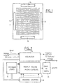
Sur la figure 1, on voit la constitution générale d'un capteur selon l'invention. Il comporte essentiellement une matrice de 128x128 éléments individuels qui sont des microcapteurs de pression disposés en réseau de lignes et colonnes.In Figure 1, we see the constitution general of a sensor according to the invention. It comprises basically a matrix of 128x128 elements individual that are pressure microsensors arranged in a network of rows and columns.
Chaque élément occupe une surface carrée d'environ 50 micromètres par 50 micromètres, ou un cercle de 50 micromètres de diamètre environ.Each element occupies a square surface about 50 microns by 50 microns, or one circle of approximately 50 micrometers in diameter.
Le pas du réseau est de préférence d'au plus 65 micromètres, c'est-à-dire que les centres de deux éléments adjacents sont séparés de 65 micromètres au plus : la surface globale de la matrice est de 8,3x8,3 millimètres carrés, suffisante pour saisir la partie centrale d'une empreinte digitale, qui est la zone la plus riche en informations. Les dimensions données ci-dessus correspondent à un exemple de réalisation; elles donnent une définition suffisamment précise de l'empreinte et sont réalisables technologiquement sans problème particulier.The pitch of the network is preferably at most 65 micrometers, that is, the centers of two adjacent elements are separated by 65 micrometers at plus: the overall surface of the matrix is 8.3x8.3 square millimeters, sufficient to grasp the part central of a fingerprint, which is the area richer in information. The dimensions given above correspond to an exemplary embodiment; they give a sufficiently precise definition of footprint and are technologically feasible without particular problem.
Les microcapteurs peuvent être réalisés selon plusieurs techniques, utilisant des effets physiques différents pour la détection de pression. Les capteurs peuvent fonctionner sur un effet capacitif, ou un effet piézoélectrique, ou un simple microcontacteur intégré dans le circuit monolithique.The microsensors can be produced according to several techniques, using physical effects different for pressure detection. The sensors can operate on a capacitive effect, or an effect piezoelectric, or a simple integrated micro-switch in the monolithic circuit.
Chaque élément peut contenir une électronique simple permettant, par comparaison avec un seuil, de transformer la variation de pression en niveau logique binaire. Each element can contain electronics simple allowing, by comparison with a threshold, to transform the pressure variation into a logic level binary.
Dans le cas d'un microcapteur à effet capacitif, l'électronique de détection des variations de pression est cependant plus complexe et ne peut pas véritablement être incorporée dans chaque microcapteur; elle doit plutôt être installée à la périphérie du capteur. On peut prévoir éventuellement d'associer un point mémoire à chaque microcapteur à l'intérieur de la matrice.In the case of an effect microsensor capacitive, electronic variation detection pressure however is more complex and cannot truly be incorporated into each microsensor; it should rather be installed on the periphery of the sensor. We can possibly plan to associate a memory point to each microsensor inside the matrix.
Dans le cas d'un microcapteur à microcontacteur, l'électronique de détection est la plus simple à réaliser. L'information binaire est fabriquée dans le microcapteur même (l'interrupteur fermé ou ouvert selon la présence ou l'absence d'une pression).In the case of a microsensor with micro switch, the detection electronics is the easier to do. Binary information is manufactured in the microsensor itself (the switch closed or open depending on the presence or absence of a pressure).
Dans les deux cas de microcapteurs à effet capacitif et piézorésistif, il est possible d'obtenir un signal analogique. Cette possibilité permet d'effecteur des traitements plus élaborés sur l'image de l'empreinte (affichage en plusieurs niveaux de gris, traitement par réseaux de neurones, etc...).In both cases of effect microsensors capacitive and piezoresistive, it is possible to obtain an analog signal. This possibility allows to perform more elaborate treatments on the image of the imprint (display in several gray levels, neural network processing, etc.).
La zone couverte de microcapteurs est désignée par la référence 12 au centre du circuit intégré monolithique. La périphérie est entourée de différents circuits qui sont notamment :
un séquenceur 14, assurant le déroulement de la saisie d'information au moment de l'application du doigt. Le séquenceur comporte au moins un compteur (14 bits de préférence), un générateur de signaux d'horloge, et un sélecteur d'adresses ;- un décodeur d'adresses de ligne 16;
- un décodeur d'adresses de colonne 18;
- un étage de sortie 20 qui comporte des circuits électroniques de détection et de traitement de signal analogique, dans le cas où les microcapteurs individuels ne comportent pas cette fonction, et des amplificateurs de sortie, pour transmettre à la sortie du capteur des informations représentant le motif de pression détecté par le réseau matriciel de microcapteurs.
- a
sequencer 14, ensuring the sequence of data entry at the time of application of the finger. The sequencer comprises at least one counter (preferably 14 bits), a clock signal generator, and an address selector; - a
line address decoder 16; - a
column address decoder 18; - an
output stage 20 which includes electronic circuits for detecting and processing analog signal, in the case where the individual microsensors do not include this function, and output amplifiers, for transmitting information representing the pattern to the output of the sensor pressure detected by the matrix network of microsensors.
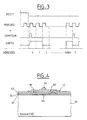
La figure 2 représente le schéma électrique du
capteur d'empreintes digitales. Le séquenceur 14 reçoit
le signal de réinitialisation (reset), une horloge
externe, et éventuellement des adresses pour
l'exploration point par point ou ligne par ligne de
l'image matricielle recueillie par les microcapteurs ;
l'image peut cependant être transmise à l'extérieur du
circuit intégré par un balayage systématique ligne par
ligne analogue à un balayage d'image vidéo, le
séquenceur comportant alors les éléments de circuit
nécessaires pour réaliser ce balayage.Figure 2 shows the electrical diagram of the
fingerprint sensor. The
Le séquenceur transmet les adresses de ligne et
de colonne aux décodeurs de ligne et de colonne (16
et 18) qui permettent d'accéder point par point aux
microcapteurs de pression de la matrice 12. Le signal
électrique en provenance d'un microcapteur adressé par
ces décodeurs est transmis sur une sortie du capteur
monolithique, à travers l'étage de sortie 20.The sequencer transmits the line addresses and
from column to row and column decoders (16
and 18) which allow point-to-point access to
La figure 3 représente les signaux de sortie du capteur, et les signaux de commande associés. Le signal de réinitialisation (Reset) définit le début d'une exploration systématique de la matrice.Figure 3 shows the output signals of the sensor, and associated control signals. The signal Reset defines the start of a systematic exploration of the matrix.
L'horloge définit le rythme d'exploration (par exemple un coup d'horloge pour chaque point de la matrice) ; les adresses successives sont incrémentées, par exemple ligne par ligne ; pour une matrice 128x128 il y a 16384 adresses successives à explorer. Le compteur de trame fournit une impulsion de remise à zéro pour définir chaque nouveau départ de transmission d'une image complète.The clock defines the pace of exploration (by example a clock tick for each point of the matrix); successive addresses are incremented, for example line by line; for a 128x128 matrix There are 16,384 successive addresses to explore. The frame counter provides a reset pulse to zero to define each new transmission start of a complete picture.
Les signaux de sortie transmis, dans le cas de résistances piézo, sont des signaux binaires représentant le dépassement ou le non dépassement d'un seuil de pression en chaque point de la matrice. Les signaux peuvent être transmis en série ou en parallèle par mots de 8 bits, 16 bits ou plus.The output signals transmitted, in the case of piezo resistors, are binary signals representing the exceeding or not exceeding of a pressure threshold at each point of the matrix. The signals can be transmitted in series or in parallel by words of 8 bits, 16 bits or more.
Dans le cas de microcontacteurs ou de condensateurs à capacité variable, le signal de sortie est analogique.In the case of microswitches or variable capacitors, the output signal is analog.
Lors d'une saisie d'empreinte digitale, le capteur entre en contact direct avec un milieu hostile. Il faut donc le protéger. Outre une couche de passivation qui termine le procédé de fabrication des circuits CMOS, on peut déposer une couche souple (de silicone par exemple) en protection finale.When entering a fingerprint, the sensor comes into direct contact with a hostile environment. It must therefore be protected. Besides a layer of passivation which completes the manufacturing process CMOS circuits, a flexible layer (of silicone for example) as final protection.
Cette couche peut être utilisée également pour améliorer la fonction de transfert de pression entre le doigt et les microcapteurs. Dans ce cas, on peut réaliser dans cette couche un plot en surépaisseur au centre de chaque microcapteur, également pour améliorer cette fonction de transfert.This layer can also be used for improve the pressure transfer function between the finger and microsensors. In this case, we can make an extra thickness in this layer at center of each microsensor, also to improve this transfer function.
La figure 4 représente une coupe d'une telle
structure avec une couche souple de protection 32
déposée sur la surface d'un substrat de circuit
intégré 30 dans lequel ont été préalablement réalisés
les microcapteurs de pression et toute l'électronique
de traitement de signal correspondante.Figure 4 shows a section of such
structure with a flexible
La couche 32 présente, au centre de chaque
microcapteur, une surépaisseur formant un plot
central 34. La surépaisseur peut être obtenue par dépôt
successif de deux couches, la première étant uniforme
et la deuxième étant déposée à travers un masque
délimitant les plots en surépaisseur.
Le matériau de la couche 32 est de préférence
du silicone, à la fois souple et résistant.The material of
Plusieurs techniques permettent de faire un capteur monolithique comportant des microcapteurs en silicium micro-usiné, compatibles avec la réalisation de circuits électroniques intégrés (de préférence en technologie CMOS).Several techniques make it possible to make a monolithic sensor comprising microsensors in micro-machined silicon, compatible with the production integrated electronic circuits (preferably in CMOS technology).
L'exemple qui suit donne une réalisation détaillée pour des microcapteurs de pression utilisant un effet piézorésistif. Le procédé est compatible avec une technologie CMOS et permet donc l'intégration sur la même puce de circuit intégré des microcapteurs et des circuits électroniques de commande et de traitement de signal.The following example gives an embodiment detailed for pressure microsensors using a piezoresistive effect. The process is compatible with CMOS technology and therefore allows integration on the same microsensors integrated circuit chip and electronic control and processing circuits signal.
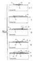
La figure 5 donne les principales étapes de réalisation.Figure 5 gives the main stages of production.
Sur un substrat de silicium 30 éventuellement
revêtu d'une fine couche d'arrêt de gravure 33 (en
nitrure de silicium), on dépose une couche
sacrificielle ou couche sacrifiée de silicium
polycristallin 35.Optionally on a
Cette couche est photogravée pour laisser subsister une zone de silicium polycristallin à l'endroit de chaque microcapteur.This layer is photo-etched to leave remain a polycrystalline silicon zone at the location of each microsensor.
On dépose ensuite une fine couche de nitrure de
silicium 36 sur toute la surface du substrat, puis une
deuxième couche de silicium polycristallin 38. Cette
deuxième couche est gravée pour réaliser des ponts de
résistances piézoélectriques (un pont de Weathstone de
4 résistances) correspondant chacun à un microcapteur
de pression.Then a thin layer of nitride of
Une ou plusieurs résistances d'un pont sont
déposées au-dessus des zones de silicium polycristallin
de la première couche. Puis, une deuxième couche de
nitrure de silicium 40 est déposée pour protéger les
résistances.One or more resistors of a bridge are
deposited above the polycrystalline silicon zones
of the first layer. Then a second layer of
L'étape suivante consiste à pratiquer des
trous 42 dans les couches de nitrure de silicium, à
côté des résistances mais au dessus des zones de la
première couche de silicium polycristallin 35.The next step is to practice
Par ces trous on accède à la première couche de
silicium polycristallin 35, à travers les deux couches
de nitrure 36 et 40.Through these holes we access the first layer of
Une gravure humide (KOH) est réalisée pour
attaquer le silicium polycristallin partout où il n'est
pas protégé. L'attaque se fait par les trous 42 et la
totalité de la couche sacrificielle 35 est enlevée à
travers ces trous. Le silicium est protégé ailleurs par
les couches de nitrure et par la couche d'arrêt de
gravure 33.Wet etching (KOH) is performed to
attack polycrystalline silicon wherever it is
not protected. The attack is made through
Une cavité 44 subsiste alors sous les
résistances piézoélectriques qui sont alors suspendues
sur une couche isolante tendue et qui peuvent subir des
déformations lorsqu'une pression est exercée sur elles.A
La couche isolante tendue est ici constituée
par les couches de nitrure de silicium 36 et 40 formant
un diaphragme 46 suspendu au dessus de la cavité 44.
Les parois latérales de la cavité sont en nitrure de
silicium. Le fond est constitué par la fine couche
d'arrêt de gravure 33 reposant sur le substrat.The stretched insulating layer is here constituted
by the layers of
La gravure terminée, on peut redéposer du
nitrure de silicium 48 pour boucher les trous 42 et
sceller ainsi les cavités. After the engraving, you can redeposit
Les circuits électroniques de commande et de traitement sont formés simultanément par des opérations de dépôt et de gravure classiques en technologie CMOS, certaines des étapes ci-dessus étant communes avec des étapes de réalisation de circuits CMOS, et toutes les étapes étant de toutes façons compatibles avec la réalisation de circuits CMOS sur le même substrat.The electronic control and treatment are formed simultaneously by operations classic CMOS deposition and engraving, some of the above steps being common with steps for making CMOS circuits, and all anyway being compatible with the creation of CMOS circuits on the same substrate.
La couche souple 32 de protection (figure 4) en silicone ou matériau analogue est déposée en fin de procédé, après les étapes de passivation finale (couches de silice ou autres) classiques dans les circuits intégrés.The flexible protective layer 32 (FIG. 4) in silicone or similar material is deposited at the end of process, after the final passivation steps (layers of silica or others) conventional in integrated circuits.
L'exemple qui suit donne une réalisation détaillée des microcapteurs de pression utilisant un effet capacitif ou des microcontacteurs. Dans les deux cas le processus de réalisation est le même, seule l'épaisseur du diaphragme change pour permettre ou non l'établissement d'un contact. Un ordre de grandeur de cette épaisseur est de 0,5 µm.The following example gives an embodiment detailed microsensor pressure using a capacitive effect or microswitches. In both case the realization process is the same, only the thickness of the diaphragm changes to allow or not establishing contact. An order of magnitude of this thickness is 0.5 µm.
Dans cet exemple de réalisation illustré par la figure 6, on a repris les même références pour désigner les mêmes éléments que ceux entrant dans la description de la figure 5.In this exemplary embodiment illustrated by the Figure 6, we used the same references to designate the same elements as those entering in the description in Figure 5.
Sur un substrat de silicium on dépose une
couche de métal (par exemple Au ou Ti) qui sera
utilisée soit comme première armature 51 d'une capacité
variable, soit comme première borne d'un
microcontacteur.On a silicon substrate is deposited a
metal layer (for example Au or Ti) which will
used either as the
Cette couche 51 est gravée pour former la
géométrie (circulaire dans cette réalisation) et
l'emplacement de l'armature.This
On dépose ensuite une couche intermédiaire de
silicium polycristallin 35 ou une couche de métal tel
que de l'aluminium (Al) (couche sacrifiée). Cette
couche 35 subit une photolithogravure pour obtenir la
géométrie (circulaire) et l'emplacement du
diaphragme 46 du microcapteur.Then an intermediate layer of
Le diaphragme 46 et l'armature 52 sont
concentriques. Une deuxième couche de
métal 52 (Au ou Ti) est déposée pour former soit la
deuxième armature de la capacité, soit la deuxième
borne du microcontacteur. Cette couche est gravée pour
laisser subsister la deuxième armature dans
l'alignement vertical de la première.The
La deuxième étape consiste à déposer une couche
fine de nitrure de silicium 36 sur toute la surface du
substrat.The second step is to deposit a
La troisième étape consiste à pratiquer un trou
sur le bord du diaphragme 36 et qui traverse la couche
de nitrure pour atteindre la couche sacrifiée. Ensuite,
une gravure humide est effectuée sur le substrat. La
solution attaque à travers le trou la couche sacrifiée.
La gravure continue jusqu'à disparition totale de la
couche sacrifiée. Une cavité est donc formée. Le
diaphragme 46 et l'armature supérieure 52 se trouvent
complètement dégagés.The third step is to practice a hole
on the edge of the
La gravure étant terminée, on effectue un dépôt
de nitrure de silicium 48 sous vide pour fermer le trou
et sceller la cavité (bouchon 48).The engraving being finished, a deposit is made
of
La dernière étape consiste à déposer une couche
de silicone 32 pour protéger l'ensemble et réaliser un
plot centré au milieu de chaque microcapteur (étape V).The last step is to deposit a layer
of
Claims (16)
- Fingerprint sensor comprising a matrix of pressure microsensors (12) sensitive to the pattern of the print of a finger, the sensor being produced on a substrate according to an integrated circuit manufacturing technology, characterised in that each microsensor of the matrix comprises a cavity (44) closed by a diaphragm (46) constituted by an insulating material to carry conducting elements of the microsensor and allow their deformations under the action of a pressure.
- Fingerprint sensor according to claim 1,
characterised in that each pressure microsensor is constituted by a bridge of piezo-electric resistors (38) deposited on a first layer of insulating material (36) forming the diaphragm. - Fingerprint sensor according to claim 2,
characterised in that the bridge of piezo-electric resistors is constituted by strips of polycrystalline silicon (38) deposited on the first insulating layer (36) stretched over the cavity (44). - Fingerprint sensor according to claim 3,
characterised in that the cavity is delimited by walls formed by this first insulating layer, the piezo-electric resistors resting on the diaphragm (46) suspended over the cavity. - Fingerprint sensor according to claim 1,
characterised in that each pressure microsensor is constituted by a microswitch the armatures of which are in the cavity, one being locked to the diaphragm (46), the other being on the substrate (30). - Fingerprint sensor according to claim 1,
characterised in that each pressure microsensor is constituted by a variable capacitor the armatures of which are in the cavity, one being locked to the diaphragm, the other being on the substrate. - Fingerprint sensor according to claims 5 or 6,
characterised in that the cavity is delimited by walls made of silicon nitride (36), a layer of metal (52) resting on the diaphragm (46) suspended over the cavity. - Fingerprint sensor according to one of the preceding claims, characterised in that the matrix comprises at least 128X128 microsensors arranged in a network with a pitch less than or equal to 65 micrometres.
- Sensor according to any one of the preceding claims,
characterised in that the microsensors are produced on a monolithic substrate and are covered with a layer (32) of flexible material such as silicone protecting the microsensors and facilitating the pressure transfer function between the finger and the microsensors. - Sensor according to claim 9, characterised in that the thickness of the layer of flexible material is reinforced in the centre of each microsensor to form a contact (34) and thus improve the pressure transfer function between the finger and the microsensors.
- Fingerprint sensor according to any one of the preceding claims, characterised in that it comprises electronic circuits comprising means (20) for transmitting electrical signals representing the pressure detected by each microsensor at an output of the sensor.
- Fingerprint sensor according to claim 11,
characterised in that the electrical signals representing the pressure detected by a microsensor are binary signals representing the overshooting or non-overshooting of a pressure threshold. - Fingerprint sensor according to any one of the preceding claims, characterised in that the output signal is analogue permitting more precise measurement of the pressure of the finger.
- Process for production of a fingerprint sensor comprising a matrix of pressure-detecting microsensors (12) sensitive to the pattern of the print of a finger and electronic circuits (14, 16, 18, 20) coupled to this means of detection and making it possible to supply electrical signals representing this pattern, the sensor being produced entirely according to an integrated circuit manufacturing technology both for the matrix of microsensors and for the electronic circuits coupled to the matrix, characterised in that it comprises the following steps:deposition of a layer of polycrystalline silicon (35) over the substrate (30) ;photo-engraving of this layer except in the locations of each microsensor;deposition of a layer of insulating material (36) over the entire surface of the substrate;deposition of a second layer of polycrystalline silicon (38);engraving of the second layer of polycrystalline silicon (38) to produce bridges of piezo-electric resistors each corresponding to a microsensor;deposition of a second layer of insulating material (40) to protect the resistors;attacking the first layer of polycrystalline silicon in the unprotected locations thus forming a cavity under the piezo-electric resistors so as to be suspended from the insulating layer formed by the layers of silicon nitride (36, 40).
- Process for producing a fingerprint sensor comprising a matrix of pressure-detecting microsensors (12) sensitive to the pattern of the print of a finger and electronic circuits (14, 16, 18, 20) coupled to this means of detection and making it possible to supply electrical signals representing this pattern, the sensor being produced according to an integrated circuit manufacturing technology both for the matrix of microsensors and for the electronic circuits coupled to the matrix, characterised in that it comprises the following steps:deposition of a layer of metal and engraving to form a first microswitch armature (51);deposition of a layer of polycrystalline silicon (35) or of metal;photo-engraving of this layer to obtain a diaphragm of desired geometry;deposition of a layer of insulating material (36) over the entire surface of the substrate;deposition of a second layer of metal and engraving to form a second microswitch armature (52);deposition of a layer of insulating material to protect the armatures;attacking the layer of polycrystalline silicon in the unprotected locations thus forming a cavity inside which the armatures are located facing one another.
- Process according to claims 14 or 15, characterised in that the layers of insulating material are layers of silicon nitride.
Applications Claiming Priority (2)
| Application Number | Priority Date | Filing Date | Title |
|---|---|---|---|
| FR9512168A FR2739977B1 (en) | 1995-10-17 | 1995-10-17 | MONOLITHIC FINGERPRINT SENSOR |
| FR9512168 | 1995-10-17 |
Publications (2)
| Publication Number | Publication Date |
|---|---|
| EP0769754A1 EP0769754A1 (en) | 1997-04-23 |
| EP0769754B1 true EP0769754B1 (en) | 2000-05-24 |
Family
ID=9483604
Family Applications (1)
| Application Number | Title | Priority Date | Filing Date |
|---|---|---|---|
| EP96402200A Expired - Lifetime EP0769754B1 (en) | 1995-10-17 | 1996-10-15 | Monolithic fingerprint sensor |
Country Status (5)
| Country | Link |
|---|---|
| US (1) | US5844287A (en) |
| EP (1) | EP0769754B1 (en) |
| JP (1) | JPH09126918A (en) |
| DE (1) | DE69608521T2 (en) |
| FR (1) | FR2739977B1 (en) |
Families Citing this family (87)
| Publication number | Priority date | Publication date | Assignee | Title |
|---|---|---|---|---|
| US5658698A (en) * | 1994-01-31 | 1997-08-19 | Canon Kabushiki Kaisha | Microstructure, process for manufacturing thereof and devices incorporating the same |
| US7613659B1 (en) | 1994-11-28 | 2009-11-03 | Yt Acquisition Corporation | System and method for processing tokenless biometric electronic transmissions using an electronic rule module clearinghouse |
| US7882032B1 (en) | 1994-11-28 | 2011-02-01 | Open Invention Network, Llc | System and method for tokenless biometric authorization of electronic communications |
| US20040128249A1 (en) | 1994-11-28 | 2004-07-01 | Indivos Corporation, A Delaware Corporation | System and method for tokenless biometric electronic scrip |
| FR2762389B1 (en) * | 1997-04-17 | 1999-05-21 | Commissariat Energie Atomique | FLEXIBLE MEMBRANE MICROSYSTEM FOR PRESSURE SENSOR AND METHOD FOR PRODUCING THE SAME |
| US6088585A (en) * | 1997-05-16 | 2000-07-11 | Authentec, Inc. | Portable telecommunication device including a fingerprint sensor and related methods |
| JP3592487B2 (en) * | 1997-07-02 | 2004-11-24 | 日本電信電話株式会社 | Fingerprint recognition integrated circuit |
| US6240199B1 (en) * | 1997-07-24 | 2001-05-29 | Agere Systems Guardian Corp. | Electronic apparatus having improved scratch and mechanical resistance |
| JP3053007B2 (en) * | 1997-07-28 | 2000-06-19 | 日本電気株式会社 | Fingerprint sensor |
| JP3102395B2 (en) * | 1997-11-27 | 2000-10-23 | 日本電気株式会社 | Fingerprint detection device |
| US6317508B1 (en) * | 1998-01-13 | 2001-11-13 | Stmicroelectronics, Inc. | Scanning capacitive semiconductor fingerprint detector |
| US5982608A (en) * | 1998-01-13 | 1999-11-09 | Stmicroelectronics, Inc. | Semiconductor variable capacitor |
| DE69922722T2 (en) * | 1998-03-05 | 2005-12-15 | Nippon Telegraph And Telephone Corp. | Surface shape recognition sensor and its manufacturing method |
| JP3873454B2 (en) * | 1998-05-29 | 2007-01-24 | 株式会社デンソー | Semiconductor pressure sensor |
| US6131464A (en) * | 1998-06-16 | 2000-10-17 | Smarttouch, Inc. | Pressure sensitive biometric input apparatus |
| JP3356401B2 (en) * | 1998-07-02 | 2002-12-16 | 日本電信電話株式会社 | Surface shape recognition sensor |
| EP0969477B1 (en) | 1998-07-02 | 2006-09-27 | Nippon Telegraph and Telephone Corporation | Small capacitance change detection device |
| RU2195048C2 (en) * | 1998-07-09 | 2002-12-20 | Инфинеон Текнолоджиз Аг | Semiconductor component with passivating layer |
| US6100107A (en) * | 1998-08-06 | 2000-08-08 | Industrial Technology Research Institute | Microchannel-element assembly and preparation method thereof |
| ATE444709T1 (en) * | 1999-08-09 | 2009-10-15 | Sonavation Inc | PIEZOELECTRIC THIN FILM FINGERPRINT SCANNER |
| JP4308376B2 (en) * | 1999-08-09 | 2009-08-05 | セイコーインスツル株式会社 | Fingerprint reader |
| CA2293118A1 (en) | 1999-12-24 | 2001-06-24 | Francis Picard | Bolometric fingerprint sensor |
| US20030001459A1 (en) * | 2000-03-23 | 2003-01-02 | Cross Match Technologies, Inc. | Secure wireless sales transaction using print information to verify a purchaser's identity |
| US7067962B2 (en) | 2000-03-23 | 2006-06-27 | Cross Match Technologies, Inc. | Multiplexer for a piezo ceramic identification device |
| AU2001245936A1 (en) * | 2000-03-23 | 2001-10-03 | Cross Match Technologies, Inc. | Piezoelectric identification device and applications thereof |
| US6578436B1 (en) | 2000-05-16 | 2003-06-17 | Fidelica Microsystems, Inc. | Method and apparatus for pressure sensing |
| US7316167B2 (en) * | 2000-05-16 | 2008-01-08 | Fidelica, Microsystems, Inc. | Method and apparatus for protection of contour sensing devices |
| US7565329B2 (en) | 2000-05-31 | 2009-07-21 | Yt Acquisition Corporation | Biometric financial transaction system and method |
| US9165323B1 (en) | 2000-05-31 | 2015-10-20 | Open Innovation Network, LLC | Biometric transaction system and method |
| NO315017B1 (en) * | 2000-06-09 | 2003-06-23 | Idex Asa | Sensor chip, especially for measuring structures in a finger surface |
| US6860154B2 (en) * | 2001-01-16 | 2005-03-01 | Fujikura Ltd. | Pressure sensor and manufacturing method thereof |
| US6515402B2 (en) * | 2001-01-24 | 2003-02-04 | Koninklijke Philips Electronics N.V. | Array of ultrasound transducers |
| KR100393191B1 (en) * | 2001-05-12 | 2003-07-31 | 삼성전자주식회사 | Fingerprint sensor using piezoelectric membrane |
| US7293467B2 (en) * | 2001-07-09 | 2007-11-13 | Nartron Corporation | Anti-entrapment system |
| US6672174B2 (en) * | 2001-07-23 | 2004-01-06 | Fidelica Microsystems, Inc. | Fingerprint image capture device with a passive sensor array |
| KR100432490B1 (en) | 2001-09-17 | 2004-05-22 | (주)니트 젠 | Optical fingerprint acquisition apparatus |
| EP1541086B1 (en) | 2002-09-17 | 2010-11-10 | Fujitsu Limited | Biological information acquiring apparatus and authentication apparatus using biological information |
| DE10245627B3 (en) * | 2002-09-30 | 2004-05-06 | Infineon Technologies Ag | fingerprint sensor |
| DE10246664A1 (en) * | 2002-10-07 | 2004-04-15 | Dorma Gmbh + Co. Kg | Access control unit has a modular design with exchangeable plug-in units that can be assembled to form an essentially autonomous unit that can also be connected to a bus system if necessary |
| JP2004138416A (en) * | 2002-10-16 | 2004-05-13 | Nihon Kaiheiki Industry Co Ltd | Pressure-sensitive fingerprint sensor |
| US7340960B2 (en) | 2004-01-30 | 2008-03-11 | Analatom Inc. | Miniature sensor |
| US8131026B2 (en) | 2004-04-16 | 2012-03-06 | Validity Sensors, Inc. | Method and apparatus for fingerprint image reconstruction |
| JP2005346271A (en) | 2004-06-01 | 2005-12-15 | Fujitsu Ltd | Fingerprint sensor package |
| EP1800243B1 (en) | 2004-10-04 | 2010-08-11 | Validity Sensors, Inc. | Fingerprint sensing assemblies comprising a substrate |
| EP1707931B1 (en) * | 2005-03-31 | 2013-03-27 | STMicroelectronics Srl | Analog data-input device provided with a microelectromechanical pressure sensor |
| US7373843B2 (en) * | 2005-06-02 | 2008-05-20 | Fidelica Microsystems | Flexible imaging pressure sensor |
| EP1762925B1 (en) * | 2005-09-09 | 2016-12-21 | STMicroelectronics Srl | Analog input device with integrated pressure sensor and electronic apparatus equipped with said input device. |
| FR2897937B1 (en) * | 2006-02-24 | 2008-05-23 | Commissariat Energie Atomique | PRESSURE SENSOR WITH RESISTIVE GAUGES |
| JP4427039B2 (en) * | 2006-08-18 | 2010-03-03 | 富士通株式会社 | Biometric information acquisition apparatus and biometric information authentication apparatus |
| WO2008088898A1 (en) | 2007-01-19 | 2008-07-24 | Sierra Scientific Instruments, Inc. | Micro-remote gastrointestinal physiological measurement device |
| CA2695489A1 (en) * | 2007-04-23 | 2008-11-06 | Sierra Scientific Instruments, Inc. | Suspended membrane pressure sensing array |
| DE102007025947B4 (en) * | 2007-06-04 | 2009-02-26 | Fraunhofer-Gesellschaft zur Förderung der angewandten Forschung e.V. | Integrated capacitive sensor |
| US8073204B2 (en) * | 2007-12-31 | 2011-12-06 | Authentec, Inc. | Hybrid multi-sensor biometric identification device |
| US8582837B2 (en) * | 2007-12-31 | 2013-11-12 | Authentec, Inc. | Pseudo-translucent integrated circuit package |
| US8116540B2 (en) | 2008-04-04 | 2012-02-14 | Validity Sensors, Inc. | Apparatus and method for reducing noise in fingerprint sensing circuits |
| EP2321764A4 (en) | 2008-07-22 | 2012-10-10 | Validity Sensors Inc | System, device and method for securing a device component |
| US8600122B2 (en) | 2009-01-15 | 2013-12-03 | Validity Sensors, Inc. | Apparatus and method for culling substantially redundant data in fingerprint sensing circuits |
| NO20093601A1 (en) | 2009-12-29 | 2011-06-30 | Idex Asa | surface Sensor |
| US8716613B2 (en) | 2010-03-02 | 2014-05-06 | Synaptics Incoporated | Apparatus and method for electrostatic discharge protection |
| US8471345B2 (en) * | 2010-03-05 | 2013-06-25 | Authentec, Inc. | Biometric sensor assembly with integrated visual indicator |
| US8378508B2 (en) | 2010-03-05 | 2013-02-19 | Authentec, Inc. | Integrally molded die and bezel structure for fingerprint sensors and the like |
| US9001040B2 (en) | 2010-06-02 | 2015-04-07 | Synaptics Incorporated | Integrated fingerprint sensor and navigation device |
| JP5213908B2 (en) * | 2010-06-03 | 2013-06-19 | 日立オムロンターミナルソリューションズ株式会社 | Biometric authentication unit |
| FR2965377A1 (en) | 2010-09-24 | 2012-03-30 | Univ D Avignon Et Des Pays De Vaucluse | METHOD FOR CLASSIFYING BIOMETRIC DATA |
| US8594393B2 (en) | 2011-01-26 | 2013-11-26 | Validity Sensors | System for and method of image reconstruction with dual line scanner using line counts |
| US8538097B2 (en) | 2011-01-26 | 2013-09-17 | Validity Sensors, Inc. | User input utilizing dual line scanner apparatus and method |
| US10112556B2 (en) | 2011-11-03 | 2018-10-30 | Ford Global Technologies, Llc | Proximity switch having wrong touch adaptive learning and method |
| US9559688B2 (en) * | 2012-04-11 | 2017-01-31 | Ford Global Technologies, Llc | Proximity switch assembly having pliable surface and depression |
| US9520875B2 (en) | 2012-04-11 | 2016-12-13 | Ford Global Technologies, Llc | Pliable proximity switch assembly and activation method |
| US9831870B2 (en) | 2012-04-11 | 2017-11-28 | Ford Global Technologies, Llc | Proximity switch assembly and method of tuning same |
| US9531379B2 (en) * | 2012-04-11 | 2016-12-27 | Ford Global Technologies, Llc | Proximity switch assembly having groove between adjacent proximity sensors |
| US9944237B2 (en) | 2012-04-11 | 2018-04-17 | Ford Global Technologies, Llc | Proximity switch assembly with signal drift rejection and method |
| US9660644B2 (en) | 2012-04-11 | 2017-05-23 | Ford Global Technologies, Llc | Proximity switch assembly and activation method |
| US9568527B2 (en) | 2012-04-11 | 2017-02-14 | Ford Global Technologies, Llc | Proximity switch assembly and activation method having virtual button mode |
| DE102012021413B4 (en) * | 2012-10-30 | 2016-06-02 | Infineon Technologies Ag | Sensor with masking |
| NO20131423A1 (en) | 2013-02-22 | 2014-08-25 | Idex Asa | Integrated fingerprint sensor |
| DE112015000883T5 (en) | 2014-02-21 | 2017-01-12 | G. Benkley Fred III | A sensor using overlapping grid lines and conductive probes to extend a sensor area from the grid lines |
| CN104134063B (en) * | 2014-08-26 | 2018-01-30 | 南昌欧菲生物识别技术有限公司 | Fingerprint recognition detection components and its electronic installation |
| US10038443B2 (en) | 2014-10-20 | 2018-07-31 | Ford Global Technologies, Llc | Directional proximity switch assembly |
| CN104700079A (en) * | 2015-03-06 | 2015-06-10 | 南昌欧菲生物识别技术有限公司 | Fingerprint recognition module and touch screen based on fingerprint recognition |
| CN104700081A (en) * | 2015-03-06 | 2015-06-10 | 南昌欧菲生物识别技术有限公司 | Fingerprint recognition device, touch screen with same and terminal device |
| US9654103B2 (en) | 2015-03-18 | 2017-05-16 | Ford Global Technologies, Llc | Proximity switch assembly having haptic feedback and method |
| US9548733B2 (en) | 2015-05-20 | 2017-01-17 | Ford Global Technologies, Llc | Proximity sensor assembly having interleaved electrode configuration |
| USD776664S1 (en) * | 2015-05-20 | 2017-01-17 | Chaya Coleena Hendrick | Smart card |
| CN106527829A (en) * | 2015-09-15 | 2017-03-22 | 神盾股份有限公司 | Capacitive sensing device and signal processing method thereof |
| US10549982B2 (en) | 2016-02-15 | 2020-02-04 | Stmicroelectronics S.R.L. | Pressure sensor encapsulated in elastomeric material, and system including the pressure sensor |
| CN110419047A (en) * | 2018-01-29 | 2019-11-05 | 华为技术有限公司 | A kind of transparent cover plate, display screen and terminal |
Family Cites Families (12)
| Publication number | Priority date | Publication date | Assignee | Title |
|---|---|---|---|---|
| US4394773A (en) * | 1980-07-21 | 1983-07-19 | Siemens Corporation | Fingerprint sensor |
| DE3114076A1 (en) * | 1981-04-08 | 1982-11-04 | M.A.N.- Roland Druckmaschinen AG, 6050 Offenbach | "BOW ROTATION PRINTING MACHINE WITH A TRANSPORT CHAIN SYSTEM" |
| US4577345A (en) * | 1984-04-05 | 1986-03-18 | Igor Abramov | Fingerprint sensor |
| GB2215914B (en) * | 1988-03-17 | 1991-07-03 | Emi Plc Thorn | A microengineered diaphragm pressure switch and a method of manufacture thereof |
| GB2244164A (en) * | 1990-05-18 | 1991-11-20 | Philips Electronic Associated | Fingerprint sensing |
| CN1018844B (en) * | 1990-06-02 | 1992-10-28 | 中国科学院兰州化学物理研究所 | Antirust dry film lubricant |
| FR2674051A1 (en) * | 1991-03-14 | 1992-09-18 | Gemplus Card Int | Device for identifying a person, especially by fingerprint detection |
| US5220838A (en) * | 1991-03-28 | 1993-06-22 | The Foxboro Company | Overpressure-protected, differential pressure sensor and method of making the same |
| JPH0758234B2 (en) * | 1992-04-16 | 1995-06-21 | 株式会社エニックス | Semiconductor matrix type fine surface pressure distribution sensor |
| JP2769661B2 (en) * | 1992-09-29 | 1998-06-25 | 三菱電機株式会社 | Semiconductor device and manufacturing method thereof |
| DE4236133C1 (en) * | 1992-10-26 | 1994-03-10 | Siemens Ag | Sensor arrangement for recording fingerprints and method for their production |
| US5637905A (en) * | 1996-02-01 | 1997-06-10 | New Jersey Institute Of Technology | High temperature, pressure and displacement microsensor |
-
1995
- 1995-10-17 FR FR9512168A patent/FR2739977B1/en not_active Expired - Fee Related
-
1996
- 1996-10-10 US US08/728,329 patent/US5844287A/en not_active Expired - Fee Related
- 1996-10-15 DE DE69608521T patent/DE69608521T2/en not_active Expired - Fee Related
- 1996-10-15 EP EP96402200A patent/EP0769754B1/en not_active Expired - Lifetime
- 1996-10-17 JP JP8295757A patent/JPH09126918A/en active Pending
Also Published As
| Publication number | Publication date |
|---|---|
| FR2739977A1 (en) | 1997-04-18 |
| US5844287A (en) | 1998-12-01 |
| DE69608521D1 (en) | 2000-06-29 |
| FR2739977B1 (en) | 1998-01-23 |
| EP0769754A1 (en) | 1997-04-23 |
| DE69608521T2 (en) | 2000-09-14 |
| JPH09126918A (en) | 1997-05-16 |
Similar Documents
| Publication | Publication Date | Title |
|---|---|---|
| EP0769754B1 (en) | Monolithic fingerprint sensor | |
| EP0813164B1 (en) | System and method for reading fingerprints | |
| US6633656B1 (en) | Microthermistor based fingerprint sensor | |
| US6759264B2 (en) | Pressure type fingerprint sensor fabrication method | |
| US6333989B1 (en) | Contact imaging device | |
| FR2755526A1 (en) | SYSTEM FOR READING DIGITAL IMPRESSIONS WITH INTEGRATED HEATING RESISTORS | |
| JPH09218006A (en) | Fingerprint sensor | |
| CN106711320A (en) | Ultrasonic fingerprint collecting device and preparation method thereof | |
| US20010028253A1 (en) | Sensor array for a capacitance measuring fingerprint sensor, and method for producing such a sensor array | |
| US5577309A (en) | Method for forming electrical contact to the optical coating of an infrared detector | |
| FR2912531A1 (en) | METHOD OF BIOMETRY BASED ON A THERMAL IMAGE OF A FINGER | |
| FR2736179A1 (en) | Access authorisation based on finger print recognition | |
| KR100914026B1 (en) | The Method for Manufacturing Fingerprint Sensor Using Piezoelectric Thin Film | |
| FR3069938A1 (en) | THERMO-RESISTIVE CAPSULE CAPTURE DEVICE ADAPTED TO PASSIVE ADDRESSING | |
| WO2004061757A1 (en) | Method of determining the living character of an element bearing a fingerprint | |
| US11237058B2 (en) | Thermal pattern sensor with pyroelectric capacitance | |
| JP2002213911A (en) | Mounting package | |
| US5552326A (en) | Method for forming electrical contact to the optical coating of an infrared detector using conductive epoxy | |
| KR100495802B1 (en) | The pixel for IR detector and method for manufacturing the same | |
| JPH10256565A (en) | Manufacture of semiconductor device having micromechanical structure | |
| FR2839173A1 (en) | Capacitive fingerprint sensor for real-time identification of fingerprint, inputs pulse control voltage to signal reading circuit comprising shutter switch to enable sense and reference capacitors to share charges | |
| US10734566B2 (en) | Thermal pattern sensor with pyroelectric capacitance and hard protective layer | |
| WO2016027028A1 (en) | Device for obtaining fingerprints | |
| CA2311914C (en) | Microthermistor based fingerprint sensor | |
| CN105556261B (en) | Infrared-ray detecting element and the infra-red ray detection device for having it |
Legal Events
| Date | Code | Title | Description |
|---|---|---|---|
| PUAI | Public reference made under article 153(3) epc to a published international application that has entered the european phase |
Free format text: ORIGINAL CODE: 0009012 |
|
| AK | Designated contracting states |
Kind code of ref document: A1 Designated state(s): DE FR GB IT |
|
| 17P | Request for examination filed |
Effective date: 19971022 |
|
| GRAG | Despatch of communication of intention to grant |
Free format text: ORIGINAL CODE: EPIDOS AGRA |
|
| 17Q | First examination report despatched |
Effective date: 19990723 |
|
| GRAG | Despatch of communication of intention to grant |
Free format text: ORIGINAL CODE: EPIDOS AGRA |
|
| GRAH | Despatch of communication of intention to grant a patent |
Free format text: ORIGINAL CODE: EPIDOS IGRA |
|
| GRAH | Despatch of communication of intention to grant a patent |
Free format text: ORIGINAL CODE: EPIDOS IGRA |
|
| GRAA | (expected) grant |
Free format text: ORIGINAL CODE: 0009210 |
|
| ITF | It: translation for a ep patent filed |
Owner name: BOTTI & FERRARI S.R.L. |
|
| AK | Designated contracting states |
Kind code of ref document: B1 Designated state(s): DE FR GB IT |
|
| REF | Corresponds to: |
Ref document number: 69608521 Country of ref document: DE Date of ref document: 20000629 |
|
| GBT | Gb: translation of ep patent filed (gb section 77(6)(a)/1977) |
Effective date: 20000620 |
|
| PLBE | No opposition filed within time limit |
Free format text: ORIGINAL CODE: 0009261 |
|
| STAA | Information on the status of an ep patent application or granted ep patent |
Free format text: STATUS: NO OPPOSITION FILED WITHIN TIME LIMIT |
|
| 26N | No opposition filed | ||
| REG | Reference to a national code |
Ref country code: GB Ref legal event code: IF02 |
|
| PGFP | Annual fee paid to national office [announced via postgrant information from national office to epo] |
Ref country code: GB Payment date: 20080926 Year of fee payment: 13 |
|
| PGFP | Annual fee paid to national office [announced via postgrant information from national office to epo] |
Ref country code: DE Payment date: 20081030 Year of fee payment: 13 |
|
| PGFP | Annual fee paid to national office [announced via postgrant information from national office to epo] |
Ref country code: IT Payment date: 20081016 Year of fee payment: 13 |
|
| PGFP | Annual fee paid to national office [announced via postgrant information from national office to epo] |
Ref country code: FR Payment date: 20081028 Year of fee payment: 13 |
|
| REG | Reference to a national code |
Ref country code: FR Ref legal event code: ST Effective date: 20100630 |
|
| PG25 | Lapsed in a contracting state [announced via postgrant information from national office to epo] |
Ref country code: FR Free format text: LAPSE BECAUSE OF NON-PAYMENT OF DUE FEES Effective date: 20091102 Ref country code: DE Free format text: LAPSE BECAUSE OF NON-PAYMENT OF DUE FEES Effective date: 20100501 |
|
| PG25 | Lapsed in a contracting state [announced via postgrant information from national office to epo] |
Ref country code: GB Free format text: LAPSE BECAUSE OF NON-PAYMENT OF DUE FEES Effective date: 20091015 |
|
| PG25 | Lapsed in a contracting state [announced via postgrant information from national office to epo] |
Ref country code: IT Free format text: LAPSE BECAUSE OF NON-PAYMENT OF DUE FEES Effective date: 20091015 |