EP0750331A2 - Procédé de fabrication d'un écran fluorescent pour un tube à rayons cathodiques - Google Patents
Procédé de fabrication d'un écran fluorescent pour un tube à rayons cathodiques Download PDFInfo
- Publication number
- EP0750331A2 EP0750331A2 EP96109791A EP96109791A EP0750331A2 EP 0750331 A2 EP0750331 A2 EP 0750331A2 EP 96109791 A EP96109791 A EP 96109791A EP 96109791 A EP96109791 A EP 96109791A EP 0750331 A2 EP0750331 A2 EP 0750331A2
- Authority
- EP
- European Patent Office
- Prior art keywords
- phosphor layer
- cathode ray
- ray tube
- forming
- water
- Prior art date
- Legal status (The legal status is an assumption and is not a legal conclusion. Google has not performed a legal analysis and makes no representation as to the accuracy of the status listed.)
- Granted
Links
Images

Classifications
-
- C—CHEMISTRY; METALLURGY
- C03—GLASS; MINERAL OR SLAG WOOL
- C03C—CHEMICAL COMPOSITION OF GLASSES, GLAZES OR VITREOUS ENAMELS; SURFACE TREATMENT OF GLASS; SURFACE TREATMENT OF FIBRES OR FILAMENTS MADE FROM GLASS, MINERALS OR SLAGS; JOINING GLASS TO GLASS OR OTHER MATERIALS
- C03C17/00—Surface treatment of glass, not in the form of fibres or filaments, by coating
- C03C17/34—Surface treatment of glass, not in the form of fibres or filaments, by coating with at least two coatings having different compositions
- C03C17/36—Surface treatment of glass, not in the form of fibres or filaments, by coating with at least two coatings having different compositions at least one coating being a metal
- C03C17/3602—Surface treatment of glass, not in the form of fibres or filaments, by coating with at least two coatings having different compositions at least one coating being a metal the metal being present as a layer
- C03C17/3607—Coatings of the type glass/inorganic compound/metal
-
- C—CHEMISTRY; METALLURGY
- C03—GLASS; MINERAL OR SLAG WOOL
- C03C—CHEMICAL COMPOSITION OF GLASSES, GLAZES OR VITREOUS ENAMELS; SURFACE TREATMENT OF GLASS; SURFACE TREATMENT OF FIBRES OR FILAMENTS MADE FROM GLASS, MINERALS OR SLAGS; JOINING GLASS TO GLASS OR OTHER MATERIALS
- C03C17/00—Surface treatment of glass, not in the form of fibres or filaments, by coating
- C03C17/34—Surface treatment of glass, not in the form of fibres or filaments, by coating with at least two coatings having different compositions
- C03C17/36—Surface treatment of glass, not in the form of fibres or filaments, by coating with at least two coatings having different compositions at least one coating being a metal
- C03C17/3602—Surface treatment of glass, not in the form of fibres or filaments, by coating with at least two coatings having different compositions at least one coating being a metal the metal being present as a layer
- C03C17/3649—Surface treatment of glass, not in the form of fibres or filaments, by coating with at least two coatings having different compositions at least one coating being a metal the metal being present as a layer made of metals other than silver
-
- C—CHEMISTRY; METALLURGY
- C03—GLASS; MINERAL OR SLAG WOOL
- C03C—CHEMICAL COMPOSITION OF GLASSES, GLAZES OR VITREOUS ENAMELS; SURFACE TREATMENT OF GLASS; SURFACE TREATMENT OF FIBRES OR FILAMENTS MADE FROM GLASS, MINERALS OR SLAGS; JOINING GLASS TO GLASS OR OTHER MATERIALS
- C03C17/00—Surface treatment of glass, not in the form of fibres or filaments, by coating
- C03C17/34—Surface treatment of glass, not in the form of fibres or filaments, by coating with at least two coatings having different compositions
- C03C17/42—Surface treatment of glass, not in the form of fibres or filaments, by coating with at least two coatings having different compositions at least one coating of an organic material and at least one non-metal coating
-
- H—ELECTRICITY
- H01—ELECTRIC ELEMENTS
- H01J—ELECTRIC DISCHARGE TUBES OR DISCHARGE LAMPS
- H01J29/00—Details of cathode-ray tubes or of electron-beam tubes of the types covered by group H01J31/00
- H01J29/02—Electrodes; Screens; Mounting, supporting, spacing or insulating thereof
- H01J29/10—Screens on or from which an image or pattern is formed, picked up, converted or stored
- H01J29/18—Luminescent screens
- H01J29/28—Luminescent screens with protective, conductive or reflective layers
-
- H—ELECTRICITY
- H01—ELECTRIC ELEMENTS
- H01J—ELECTRIC DISCHARGE TUBES OR DISCHARGE LAMPS
- H01J9/00—Apparatus or processes specially adapted for the manufacture, installation, removal, maintenance of electric discharge tubes, discharge lamps, or parts thereof; Recovery of material from discharge tubes or lamps
- H01J9/20—Manufacture of screens on or from which an image or pattern is formed, picked up, converted or stored; Applying coatings to the vessel
- H01J9/22—Applying luminescent coatings
- H01J9/221—Applying luminescent coatings in continuous layers
- H01J9/224—Applying luminescent coatings in continuous layers by precipitation
Definitions
- the present invention relates to a method of producing a cathode-ray tube, more particularly relates to a method of forming a fluorescent screen of a cathode ray tube in which improves a process of pouring covering water performed between a process of forming a phosphor layer by a precipitation process and a process of forming a lacquer intermediate film.
- a cathode ray tuba is provided with a glass bulb comprising a panel portion, a funnel portion, and a neck portion and is configured so that a phosphor layer formed on an inner surface of the panel portion is irradiated by electrons from an electron gun to cause the phosphor to emit light.
- cathode ray tube for example, a cathode ray tube for a projection television or a cathode ray tube for a monochrome television is produced in for example the following way.
- the inner surface of the glass bulb on which the phosphor layer is formed is washed by using pure water etc., then an aqueous electrolyte solution such as an aqueous solution of barium acetate is poured, then a suspension obtained by dispersing the phosphor in an aqueous solution of water glass is poured in as a binder and the assembly is allowed to stand for a predetermined time to cause the phosphor to precipitate. After the precipitation of the phosphor, the glass bulb is slowly moved and inclined (tilted) so as to form the phosphor layer.
- an aqueous electrolyte solution such as an aqueous solution of barium acetate
- a suspension obtained by dispersing the phosphor in an aqueous solution of water glass is poured in as a binder and the assembly is allowed to stand for a predetermined time to cause the phosphor to precipitate.
- the glass bulb is slowly moved and inclined (tilted) so as to form the phosphor layer.
- the phosphor layer is moistened by pure water or the like, the majority of the phosphor layer is covered by a film of the water, then an organic solvent lacquer mainly composed of an acrylic resin is sprayed to form a very thin lacquer intermediate film on the film of water.
- the phosphor layer is not formed on the inner surface of the funnel portion and neck portion, so the lacquer intermediate film formed on the portion is removed by pouring pure water. This is because, when the lacquer intermediate film is formed in a region not coated with the phosphor layer, the aluminum vapor deposited film formed on this region swells by the subsequent baking step and peeling is caused from the funnel portion of the cathode ray tube.
- the phosphor layer is dried by using dehumidified air etc. and a carbon film is coated on the predetermined region and dried. Finally, the aluminum is vapor deposited to form the aluminum vapor deposited film, then the organic material used when forming the phosphor layer is heated to 400 to 440°C to decompose and remove it. The phosphor layer is formed after these steps.
- the dried phosphor is adhered to the panel glass by the water glass. For this reason, when the amount of the water glass is too small, the phosphor becomes apt to peel off due to the lowering of the bonding force with the panel glass. Conversely, if it is too large, burning occurs with aging after the fabrication of the CRT. This becomes a cause of the lowering of the luminance.
- the present invention was made in consideration with such disadvantages and has as an object thereof to provide a method of producing a cathode ray tube which forms a phosphor layer having a good surface quality by properly managing the dissolution of the water glass and barium acetate occurring in the covering water step and can improve the uniformity.
- a method of forming a fluorescent screen for a cathode ray tube having a glass bulb comprising the steps of: cleaning an inner surface of the glass bulb having a Panel portion by using at least pure water; injecting an aqueous solution of electrolyte into the glass bulb; depositing a suspension of water glass and phosphor slurry on an inner surface of the panel portion; drying the suspension to form a phosphor layer; coating a whole surface of the phosphor layer with pure water from 30 to 180 seconds; spraying a lacquer comprising an acrylic resin on the wetted phosphor layer to form a lacquer film layer; forming a metal backing layer on the lacquer film layer; and heating the glass bulb to remove the lacquer film layer at a temperature at 400 °C to 420 °C.
- the cleaning process comprises the step of cleaning the inner surface of the glass bulb by using an aqueous solution of fluorhydric acid before using the pure water, or the step of cleaning the inner surface of the glass bulb by using nitric acid before using the pure water.
- the aqueous solution of electrolyte comprises an aqueous solution of barium acetate.
- the drying process is drying the suspension by using dehumidified air.
- the coating process includes the step of coating a whole surface of the phosphor layer with pure water for 40 to 150 seconds or the step of coating process includes the step of coating a hole surface of the phosphor layer with pure water for 80 to 120 seconds.
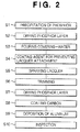
- a cathode ray tube (CRT) to which the present embodiment is applied is a CRT used in for example a projection television or a monochrome television such as a black and white television.
- the CRT hag a glass bulb 10 comprising a panel portion 12, a funnel portion 14, and a neck portion 16 and is configured so that a phosphor layer 2 formed on the inner surface of the panel portion 12 is irradiated by electrons from an electron gun (not illustrated) to cause the phosphor included in the phosphor layer 2 to emit light.
- the lacquer intermediate film 4 is formed on the front surface of this phosphor layer 2.
- the lacquer intermediate film 4 is constituted by a organic solvent lacquer comprised mainly of an acrylic resin which is dissolved into organic solvent such as toluene.
- a carbon film 8 for conduction is formed on a predetermined region of the inner surface of the funnel portion 14. Further, on the inner surface of the panel portion 12 and the funnel portion 14, an aluminum vapor deposited film 6 is formed for the purpose of prevention of ion burning of the phosphor due to the electron beam, of increase of the light emission efficiency, etc.
- the inner surface of the glass bulb 10 forming the phosphor layer 2 is washed (cleaned) by using an aqueous solution of hydrofluoric acid, an aqueous solution of nitric acid, and pure water. Subsequently, the panel portion 12 of the glass bulb 10 is turned downward, and a predetermined amount of an aqueous electrolyte solution such as an aqueous solution of barium acetate is poured (injected) into the glass bulb 10. Thereafter, a suspension obtained by dispersing a predetermined phosphor is poured (injected) into an aqueous solution of water glass serving as a binder and the assembly is allowed to stand for a predetermined time to cause the phosphor to precipitate (step 1: S1). After the precipitation of the phosphor, the glass bulb is slowly moved and inclined, to thereby form the phosphor layer 2. In this case, the drying of the phosphor layer 2 is carried out by vacuum drying etc (step 2:S2),
- the phosphor layer 2 is moistened by pure water (covering water) etc. and the whole surface of the phosphor layer 2 is covered by a film of water (step 3:S3).
- the agent (liquid) for preventing adhesion of the lacquer on the inner surface of the funnel 14, is coated below the connection portion 18 of the panel 12 and the funnel 14 and on the neck 16 (step 4:S4).
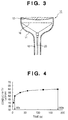
- the barium acetate and the water glass contained in the phosphor layer 2 are dissolved in the pure water, so the electric conductivity in the covering water is increased along with an increase of the time of moistening by the pure water as shown in Fig. 4.
- the production of the best cathode ray tube is made possible.
- the best cathode ray tube can be obtained when the conductivity of the electrolyte remaining in the phosphor layer after the covering water pouring process (injection process) is 6.0 ⁇ 4.0 ⁇ S/cm in 200 ml of pure water of 20°C ⁇ 1°C.
- the moistening time was set so that the conductivity of the electrolyte remaining in the phosphor layer in the covering water pouring process satisfied the above conductivity range.
- the covering water pouring process was carried out by pure water for 30 to 180 seconds.
- the panel portion 12 of the glass bulb 10 is turned upward as shown in Fig. 3 and an organic solvent lacquer mainly composed of an acrylic resin is sprayed to the inner surface of the panel portion 12 and the funnel portion 14 by using a nozzle 20 (step 5:S5) so as to form a very thin lacquer intermediate film 4 on the film of water.
- the lacquer intermediate film 4 Since if the lacquer intermediate film 4 were formed on a region on which the phosphor layer 2 was not coated, the aluminum vapor deposited film 6 deposited on this region by vapor deposition would blister in the baking process after this and peel from the funnel portion 14 of the cathode ray tube, as indicated by two dot chain line in Fig. 1, the lacquer intermediate film 4 from the funnel portion 14 to the neck portion 16 on which the phosphor layer 2 is not formed is removed by spraying pure water (trimming step 6:S6).
- the phosphor layer 2 is dried by using dehumidified air etc. (step 7:S7), then carbon for conduction is coated on a predetermined region of the inner surface of the glass bulb 10 and dried to form the carbon film 8 (step 8:S8)
- the aluminum is vapor deposited on the phosphor layer 2 to form the aluminum vapor deposited film 6, then the organic material used when forming the phosphor layer 2 is heated to 400 to 420°C to decompose and remove it (step 9:S9).
- a phosphor layer is formed on an inner surface of a panel portion of a glass bulb by a precipitation process and a lacquer intermediate film is formed on the phosphor layer in a state where the phosphor layer is moistened by covering water, characterized in that after the phosphor layer is moistened by the covering water, an electrolyte remaining in the phosphor layer has a conductivity of 6.0 ⁇ 4.0 ⁇ s/cm in 200 ml of pure water of 20°C ⁇ 1°C.
- the phosphor layer is preferably moistened by the covering water for 30 to 180 seconds.
- a phosphor layer is formed on the inner surface of the panel portion of the glass bulb by a precipitation process and a lacquer intermediate film is formed on the phosphor layer in a state where the phosphor layer is moistened by covering water.
- covering water such as pure water
- the electrolyte remaining in the phosphor layer after moistening the phosphor layer by the covering water is given a conductivity of 6.0+4.0 ⁇ s/cm in 200 ml of pure water of 20°C ⁇ 1°C.
- the amount of the electrolyte dissolved in the covering water is maintained in a proper range.
- the deterioration of the luminance of the peripheral portions of the screen after the fabrication of the CRT due to the shortage of the amount of dissolution of the electrolyte in other words, the residual presence of a large amount of the electrolyte in the phosphor layer, can be prevented.
- the detachment of the phosphor due to an excessive amount of dissolution of the electrolyte in other words, a shortage of the electrolyte remaining in the phosphor layer, can be prevented.
- the amount of the electrolyte contained in the phosphor layer dissolved in the covering water is correlated with the time of moistening with the covering water, therefore when the change of the conductivity of the electrolyte remaining in the phosphor layer with respect to the time of moistening by the covering water is preliminarily measured and the conductivity is managed by a moistening time (for example 30 to 180 seconds) satisfying the conductivity of 6.0 ⁇ 4.0 ⁇ s/cm with which the screen quality becomes the best, the management of production of the cathode ray tube becomes easier.
- a moistening time for example 30 to 180 seconds
- the luminance was improved by about 10 percent compared with a conventional cathode ray tube.
Landscapes
- Chemical & Material Sciences (AREA)
- Engineering & Computer Science (AREA)
- Life Sciences & Earth Sciences (AREA)
- Chemical Kinetics & Catalysis (AREA)
- General Chemical & Material Sciences (AREA)
- Geochemistry & Mineralogy (AREA)
- Materials Engineering (AREA)
- Organic Chemistry (AREA)
- Manufacturing & Machinery (AREA)
- Inorganic Chemistry (AREA)
- Formation Of Various Coating Films On Cathode Ray Tubes And Lamps (AREA)
- Manufacture Of Electron Tubes, Discharge Lamp Vessels, Lead-In Wires, And The Like (AREA)
Applications Claiming Priority (3)
| Application Number | Priority Date | Filing Date | Title |
|---|---|---|---|
| JP7154802A JPH097517A (ja) | 1995-06-21 | 1995-06-21 | 陰極線管の製造方法 |
| JP154802/95 | 1995-06-21 | ||
| JP15480295 | 1995-06-21 |
Publications (3)
| Publication Number | Publication Date |
|---|---|
| EP0750331A2 true EP0750331A2 (fr) | 1996-12-27 |
| EP0750331A3 EP0750331A3 (fr) | 1997-05-28 |
| EP0750331B1 EP0750331B1 (fr) | 2002-09-11 |
Family
ID=15592216
Family Applications (1)
| Application Number | Title | Priority Date | Filing Date |
|---|---|---|---|
| EP96109791A Expired - Lifetime EP0750331B1 (fr) | 1995-06-21 | 1996-06-18 | Procédé de fabrication d'un écran fluorescent pour un tube à rayons cathodiques |
Country Status (6)
| Country | Link |
|---|---|
| US (1) | US5723170A (fr) |
| EP (1) | EP0750331B1 (fr) |
| JP (1) | JPH097517A (fr) |
| CN (1) | CN1146063A (fr) |
| DE (1) | DE69623542T2 (fr) |
| SG (1) | SG67353A1 (fr) |
Cited By (2)
| Publication number | Priority date | Publication date | Assignee | Title |
|---|---|---|---|---|
| CN101840825B (zh) * | 2009-03-17 | 2011-12-28 | 东莞市兆显电子科技有限公司 | 扁平管丝印荧光粉的调制工艺 |
| WO2012037589A3 (fr) * | 2010-09-23 | 2012-06-21 | Inova Lisec Technologiezentrum Gmbh | Procédé et agent de traitement d'objets en verre |
Families Citing this family (4)
| Publication number | Priority date | Publication date | Assignee | Title |
|---|---|---|---|---|
| US6015587A (en) * | 1998-03-16 | 2000-01-18 | Industrial Technology Research Institute | Low temperature method for phosphor screen formation |
| JP3509778B2 (ja) * | 2001-06-01 | 2004-03-22 | ソニー株式会社 | 陰極線管及び陰極線管の製造方法 |
| US9234128B2 (en) * | 2012-08-27 | 2016-01-12 | General Electric Company | Chemical bleaching for improved performance of recycled lamp phosphors |
| CN115156009A (zh) * | 2022-06-13 | 2022-10-11 | 无锡机电高等职业技术学校 | 一种提高电子束荧光屏亮度的工艺方法 |
Citations (6)
| Publication number | Priority date | Publication date | Assignee | Title |
|---|---|---|---|---|
| JPS5835860A (ja) * | 1981-08-27 | 1983-03-02 | Mitsubishi Electric Corp | 光源用陰極線管 |
| DE3427009A1 (de) * | 1984-07-21 | 1986-01-23 | Licentia Patent-Verwaltungs-Gmbh, 6000 Frankfurt | Sedimentationsverfahren zum herstellen eines leuchtschirms |
| JPS61207483A (ja) * | 1985-03-11 | 1986-09-13 | Toshiba Corp | 投写管用白色発光スクリ−ン及びその製造方法 |
| EP0261732A2 (fr) * | 1986-09-20 | 1988-03-30 | Philips Patentverwaltung GmbH | Procédé de fabrication d'écrans luminescents |
| JPH01122544A (ja) * | 1987-11-06 | 1989-05-15 | Hitachi Ltd | 陰極線管の蛍光膜形成方法 |
| JPH02230630A (ja) * | 1989-03-02 | 1990-09-13 | Toshiba Corp | 陰極線管の蛍光面形成方法 |
Family Cites Families (5)
| Publication number | Priority date | Publication date | Assignee | Title |
|---|---|---|---|---|
| JPS5650031A (en) * | 1979-09-28 | 1981-05-07 | Hitachi Ltd | Manufacture of fluorescent film of picture tube |
| JP2983585B2 (ja) * | 1990-07-19 | 1999-11-29 | 三菱レイヨン株式会社 | Crtアルミバック用アンダーコート被膜の形成方法 |
| DE4036239A1 (de) * | 1990-11-14 | 1992-05-21 | Nokia Unterhaltungselektronik | Verfahren zum lackieren der leuchtstoffschicht einer farbbildroehre |
| US5366759A (en) * | 1990-11-14 | 1994-11-22 | Nokia (Deutschland) Gmbh | Method of lacquering the luminophore layer of a color picture tube |
| JPH06264054A (ja) * | 1993-03-11 | 1994-09-20 | Nichia Chem Ind Ltd | 陰極線管用蛍光体の製造方法 |
-
1995
- 1995-06-21 JP JP7154802A patent/JPH097517A/ja not_active Abandoned
-
1996
- 1996-06-18 US US08/665,442 patent/US5723170A/en not_active Expired - Fee Related
- 1996-06-18 DE DE69623542T patent/DE69623542T2/de not_active Expired - Fee Related
- 1996-06-18 EP EP96109791A patent/EP0750331B1/fr not_active Expired - Lifetime
- 1996-06-20 SG SG1996010113A patent/SG67353A1/en unknown
- 1996-06-21 CN CN96110423A patent/CN1146063A/zh active Pending
Patent Citations (6)
| Publication number | Priority date | Publication date | Assignee | Title |
|---|---|---|---|---|
| JPS5835860A (ja) * | 1981-08-27 | 1983-03-02 | Mitsubishi Electric Corp | 光源用陰極線管 |
| DE3427009A1 (de) * | 1984-07-21 | 1986-01-23 | Licentia Patent-Verwaltungs-Gmbh, 6000 Frankfurt | Sedimentationsverfahren zum herstellen eines leuchtschirms |
| JPS61207483A (ja) * | 1985-03-11 | 1986-09-13 | Toshiba Corp | 投写管用白色発光スクリ−ン及びその製造方法 |
| EP0261732A2 (fr) * | 1986-09-20 | 1988-03-30 | Philips Patentverwaltung GmbH | Procédé de fabrication d'écrans luminescents |
| JPH01122544A (ja) * | 1987-11-06 | 1989-05-15 | Hitachi Ltd | 陰極線管の蛍光膜形成方法 |
| JPH02230630A (ja) * | 1989-03-02 | 1990-09-13 | Toshiba Corp | 陰極線管の蛍光面形成方法 |
Non-Patent Citations (5)
| Title |
|---|
| DATABASE WPI Section Ch, Week 8126 Derwent Publications Ltd., London, GB; Class L03, AN 81-46460D XP002028377 & JP 56 050 031 A (HITACHI KK) , 7 May 1981 * |
| PATENT ABSTRACTS OF JAPAN vol. 007, no. 115 (E-176), 19 May 1983 & JP 58 035860 A (MITSUBISHI DENKI KK), 2 March 1983, * |
| PATENT ABSTRACTS OF JAPAN vol. 011, no. 043 (C-402), 7 February 1987 & JP 61 207483 A (TOSHIBA CORP), 13 September 1986, * |
| PATENT ABSTRACTS OF JAPAN vol. 013, no. 366 (E-806), 15 August 1989 & JP 01 122544 A (HITACHI LTD;OTHERS: 01), 15 May 1989, * |
| PATENT ABSTRACTS OF JAPAN vol. 014, no. 541 (E-1007), 29 November 1990 & JP 02 230630 A (TOSHIBA CORP), 13 September 1990, * |
Cited By (2)
| Publication number | Priority date | Publication date | Assignee | Title |
|---|---|---|---|---|
| CN101840825B (zh) * | 2009-03-17 | 2011-12-28 | 东莞市兆显电子科技有限公司 | 扁平管丝印荧光粉的调制工艺 |
| WO2012037589A3 (fr) * | 2010-09-23 | 2012-06-21 | Inova Lisec Technologiezentrum Gmbh | Procédé et agent de traitement d'objets en verre |
Also Published As
| Publication number | Publication date |
|---|---|
| JPH097517A (ja) | 1997-01-10 |
| DE69623542D1 (de) | 2002-10-17 |
| EP0750331B1 (fr) | 2002-09-11 |
| DE69623542T2 (de) | 2003-01-09 |
| CN1146063A (zh) | 1997-03-26 |
| SG67353A1 (en) | 1999-09-21 |
| EP0750331A3 (fr) | 1997-05-28 |
| US5723170A (en) | 1998-03-03 |
Similar Documents
| Publication | Publication Date | Title |
|---|---|---|
| US5723170A (en) | Method of forming fluorescent screen of cathode ray tube | |
| US3979632A (en) | Cathode ray tube having surface charge inhibiting means therein | |
| US5820921A (en) | Method of producing a cathode ray tube | |
| US5820920A (en) | Method of producing cathode ray tube | |
| JPH02306525A (ja) | メタルバックカラーブラウン管のパネル及びその製造方法 | |
| JP2650924B2 (ja) | 電子ビーム管およびその製造方法 | |
| GB2221087A (en) | Method of manufacturing phosphor screens for cathode ray tubes | |
| JPH11283530A (ja) | 陰極線管及びその製造方法 | |
| US4463075A (en) | Process for forming conductive bridge in cathode ray tubes | |
| US3893877A (en) | Method and structure for metalizing a cathode ray tube screen | |
| JP2536409B2 (ja) | 陰極線管の蛍光面形成方法 | |
| JPS6329947B2 (fr) | ||
| JP2509354B2 (ja) | 薄膜elパネルの製造方法 | |
| JPS60254536A (ja) | 陰極線管の製造方法 | |
| JPH0220749Y2 (fr) | ||
| KR940007646B1 (ko) | 필르밍액 조성물 및 이를 사용한 음극선관의 형광면 제조방법 | |
| KR100228785B1 (ko) | 칼라브라운관의 형광면 | |
| KR100189418B1 (ko) | 패널의 알루미늄막 증착방법 | |
| JPS6084737A (ja) | 光源用陰極線管の製造方法 | |
| KR100228786B1 (ko) | 칼라브라운관의 형광면 | |
| KR100258916B1 (ko) | 칼라음극선관과 그 형광막 형성방법 | |
| JPH07147130A (ja) | 陰極線管の製造方法 | |
| KR0179122B1 (ko) | 칼라 수상관의 스크린 형성 방법 | |
| JPH0311057B2 (fr) | ||
| JP2003317614A (ja) | 蛍光面基板の製造方法および蛍光面基板 |
Legal Events
| Date | Code | Title | Description |
|---|---|---|---|
| PUAI | Public reference made under article 153(3) epc to a published international application that has entered the european phase |
Free format text: ORIGINAL CODE: 0009012 |
|
| AK | Designated contracting states |
Kind code of ref document: A2 Designated state(s): DE GB |
|
| PUAL | Search report despatched |
Free format text: ORIGINAL CODE: 0009013 |
|
| AK | Designated contracting states |
Kind code of ref document: A3 Designated state(s): DE GB |
|
| 17P | Request for examination filed |
Effective date: 19971029 |
|
| 17Q | First examination report despatched |
Effective date: 19980309 |
|
| GRAG | Despatch of communication of intention to grant |
Free format text: ORIGINAL CODE: EPIDOS AGRA |
|
| GRAG | Despatch of communication of intention to grant |
Free format text: ORIGINAL CODE: EPIDOS AGRA |
|
| GRAH | Despatch of communication of intention to grant a patent |
Free format text: ORIGINAL CODE: EPIDOS IGRA |
|
| GRAH | Despatch of communication of intention to grant a patent |
Free format text: ORIGINAL CODE: EPIDOS IGRA |
|
| GRAA | (expected) grant |
Free format text: ORIGINAL CODE: 0009210 |
|
| AK | Designated contracting states |
Kind code of ref document: B1 Designated state(s): DE GB |
|
| REG | Reference to a national code |
Ref country code: GB Ref legal event code: FG4D |
|
| REF | Corresponds to: |
Ref document number: 69623542 Country of ref document: DE Date of ref document: 20021017 |
|
| PLBE | No opposition filed within time limit |
Free format text: ORIGINAL CODE: 0009261 |
|
| STAA | Information on the status of an ep patent application or granted ep patent |
Free format text: STATUS: NO OPPOSITION FILED WITHIN TIME LIMIT |
|
| 26N | No opposition filed |
Effective date: 20030612 |
|
| PGFP | Annual fee paid to national office [announced via postgrant information from national office to epo] |
Ref country code: DE Payment date: 20080626 Year of fee payment: 13 |
|
| PGFP | Annual fee paid to national office [announced via postgrant information from national office to epo] |
Ref country code: GB Payment date: 20080618 Year of fee payment: 13 |
|
| GBPC | Gb: european patent ceased through non-payment of renewal fee |
Effective date: 20090618 |
|
| PG25 | Lapsed in a contracting state [announced via postgrant information from national office to epo] |
Ref country code: GB Free format text: LAPSE BECAUSE OF NON-PAYMENT OF DUE FEES Effective date: 20090618 |
|
| PG25 | Lapsed in a contracting state [announced via postgrant information from national office to epo] |
Ref country code: DE Free format text: LAPSE BECAUSE OF NON-PAYMENT OF DUE FEES Effective date: 20100101 |