EP0748051A2 - Système et procédé pour la reconfiguration dynamique d'un réseau de portes programmables - Google Patents
Système et procédé pour la reconfiguration dynamique d'un réseau de portes programmables Download PDFInfo
- Publication number
- EP0748051A2 EP0748051A2 EP96480061A EP96480061A EP0748051A2 EP 0748051 A2 EP0748051 A2 EP 0748051A2 EP 96480061 A EP96480061 A EP 96480061A EP 96480061 A EP96480061 A EP 96480061A EP 0748051 A2 EP0748051 A2 EP 0748051A2
- Authority
- EP
- European Patent Office
- Prior art keywords
- programming
- array
- logic
- word
- logic cell
- Prior art date
- Legal status (The legal status is an assumption and is not a legal conclusion. Google has not performed a legal analysis and makes no representation as to the accuracy of the status listed.)
- Withdrawn
Links
Images


Classifications
-
- H—ELECTRICITY
- H03—ELECTRONIC CIRCUITRY
- H03K—PULSE TECHNIQUE
- H03K19/00—Logic circuits, i.e. having at least two inputs acting on one output; Inverting circuits
- H03K19/02—Logic circuits, i.e. having at least two inputs acting on one output; Inverting circuits using specified components
- H03K19/173—Logic circuits, i.e. having at least two inputs acting on one output; Inverting circuits using specified components using elementary logic circuits as components
- H03K19/177—Logic circuits, i.e. having at least two inputs acting on one output; Inverting circuits using specified components using elementary logic circuits as components arranged in matrix form
- H03K19/17748—Structural details of configuration resources
- H03K19/17752—Structural details of configuration resources for hot reconfiguration
-
- H—ELECTRICITY
- H03—ELECTRONIC CIRCUITRY
- H03K—PULSE TECHNIQUE
- H03K19/00—Logic circuits, i.e. having at least two inputs acting on one output; Inverting circuits
- H03K19/02—Logic circuits, i.e. having at least two inputs acting on one output; Inverting circuits using specified components
- H03K19/173—Logic circuits, i.e. having at least two inputs acting on one output; Inverting circuits using specified components using elementary logic circuits as components
- H03K19/177—Logic circuits, i.e. having at least two inputs acting on one output; Inverting circuits using specified components using elementary logic circuits as components arranged in matrix form
- H03K19/17704—Logic circuits, i.e. having at least two inputs acting on one output; Inverting circuits using specified components using elementary logic circuits as components arranged in matrix form the logic functions being realised by the interconnection of rows and columns
-
- H—ELECTRICITY
- H03—ELECTRONIC CIRCUITRY
- H03K—PULSE TECHNIQUE
- H03K19/00—Logic circuits, i.e. having at least two inputs acting on one output; Inverting circuits
- H03K19/02—Logic circuits, i.e. having at least two inputs acting on one output; Inverting circuits using specified components
- H03K19/173—Logic circuits, i.e. having at least two inputs acting on one output; Inverting circuits using specified components using elementary logic circuits as components
- H03K19/177—Logic circuits, i.e. having at least two inputs acting on one output; Inverting circuits using specified components using elementary logic circuits as components arranged in matrix form
- H03K19/17748—Structural details of configuration resources
- H03K19/17756—Structural details of configuration resources for partial configuration or partial reconfiguration
Definitions
- This invention relates in general to programmable integrated circuit devices. More particularly, the present invention relates to a programmable array having dynamic reconfiguration capability.
- Programmable integrated circuits are known in the art and include programmable logic devices ("PLDs”), Programmable Array Logic (“PALs”), and Programmable Logic Arrays (“PLAs"). Each of these programmable circuits provides an input AND logic plane followed by an OR logic plane. An output function comprising the sum of the products of the input terms can thus be calculated.
- the logic planes are usually programmable such that the initial general layout of the planes may be customized for a particular application.
- a more general approach to programmable circuits involves providing an array of distinct, uncommitted logic cells in a Programmable Gate Array ("PGA").
- PGA Programmable Gate Array
- a programmable interconnect network is usually provided to interconnect the cells, and to provide data input to, and output from, the array.
- Customization or programming of the otherwise generally-designed logic cells and interconnect network is performed for a particular application.
- One such array is a Mask Programmable Gate Array (“MPGA”), in which the configuration of the cells and the wiring network occurs when adding the final layers of metallization to an integrated circuit.
- MPGA Mask Programmable Gate Array
- a modified approach involves the use of laser-directed energy to customize the metallization pattern.
- FPGA Field Programmable Gate Array
- Such configuration may be effected by using electrically programmable fusible links, antifuses, memory-controlled transistors, or floating-gate transistors. All of the above referenced types of programmable logic integrated circuits are referred to herein as "programmable arrays.”
- a state machine 17 within an FPGA 13 reads a parallel or sequential programming bit stream from a Read Only Memory (“ROM”) 11 external to FPGA 13.
- ROM Read Only Memory
- the programming bit stream is read into the FPGA over data path 23 and is appropriately directed to individual programming cells of each logic cell 19 within the FPGA over data path 21.
- Conventional control communications are implemented between RAM 11 and state machine 17 to facilitate the data transfer.
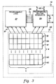
- FPGAs contain an array 15 of logic cells 19 interconnected by horizontal and vertical interconnects 25. These horizontal and vertical interconnects 25 comprise inter-cell programmable routing resources which facilitate communications between logic cells.
- a programming word 31 Connected within each logic cell 19 of the FPGA is a programming word 31 ( Fig. 2 ).
- This programming word includes the above-described programming cells as bits (33a-33h) therein. Although, as an example, an 8 bit programming word is shown, programming words may comprise 1xN (N>1) bit register structures, wherein N is sized as needed to adequately control the logic cell.
- N is sized as needed to adequately control the logic cell.
- Conventional logic cell 19 can only be used for a single programmed function at a time. Reconfiguration of the logic cell requires reactivation of the state machine and rewriting of the programming words. Such reprogramming during functional operation of the FPGA is possible, but requires relatively large delays and at least partial disruption of operations of the particular logic cell being reloaded.
- FPGAs are more flexible than their prior mask programmed counterparts, even moderately complex logic functions can only be implemented using large silicon areas. This results from the data-flow oriented nature of FPGAs. Specifically, data is passed from programmed logic cell to programmed logic cell with a preprogrammed logic function applied at each logic cell. Because each logic cell has a large overhead for providing a single programmed function, not to mention the large overhead associated with the programmable routing resources, overall FPGA logic densities remain low. Furthermore, these conventional datapath-oriented implementations suffer penalties in the areas of timing and performance due to inconsistencies in signal routing for different bits in the datapath.
- the present invention is directed toward solving the above-noted problems.
- the present invention includes a configuration system for a logic cell within a programmable array ("PA").
- the configuration system comprises a plurality of programming words simultaneously stored in the PA, of which each programming word is engagable to control a configuration of the logic cell. Further included is a means to engage a selected programming word of the plurality of programming words to control the configuration of the logic cell.
- the plurality of programming words may comprise a programming array within which each programming word may have, for example, N bits (N > 1). Further, the programming array may comprise a static random access memory (“SRAM”) array having M x N bits.
- SRAM static random access memory
- the means to engage may comprise a programmable counter for sequentially engaging different programming words of the programming array.
- the programmable counter may even comprise at least one other logic cell of the PA.
- the present invention comprises a method for configuring a logic cell within a programmable array.
- the logic cell is controllable by each programming word of a plurality of programming words associated with the logic cell and simultaneously stored in the PA.
- the method includes determining a selected programming word of the plurality of programming words and engaging it to control the configuration of the logic cell.
- the method may include engaging a different selected programming word, or engaging a sequence of selected programming words.
- the plurality of programming words may be preprogrammed, and further, reprogrammed. Individual programming words may be reprogrammed without reprogramming other programming words.
- the logic cell of the present invention may be within an IC chip.
- the IC chip may comprise many different types of IC chips within which the logic cell would be useful including, for example, a Field Programmable Gate Array, a microprocessor, or an Application Specific Integrated Circuit.
- the present invention has many advantages and features associated with it.
- the FPGA architecture disclosed resolves problems in both density and timing that are associated with data-flow based FPGA architectures.
- By providing alternate configurations of an array of logic cells many more virtual logic cells are provided. This greatly enhances the functionality and capabilities of even a moderately sized array of logic cells.
- the reduction in actual physical logic cells needed to implement a function means that data spends more time resident in a single cell, and less time in transit between cells in the unpredictable timing environment of the inter-cell routing.
- the control-flow architecture of the present invention therefore yields significant timing improvements.
- the features of the present invention expand and enhance the capabilities of field programmable gate arrays.
- a logic cell is coupled to an array of programming words referred to herein as a programming array.
- the output of the programming array comprises a selected programming word that serves as a configuration input to the programmable logic and programmable routing resources in the logic cell thereby facilitating configuration thereof.
- a logic cell 19 includes a programming array 50 including, for example, programming words 31, 39, 41, . . . 43 and 45.
- programming array 50 comprises an array of M programming words of N bits each, forming an M x N programming array.
- a selected programming word of the programming array is coupled to the programmable logic 27 and programmable routing resources 29 through data paths 37 such that the logic cell is appropriately configured.
- Such selective coupling can be performed by many techniques that will be apparent to one of ordinary skill in the art such as, for example, multiplexing and transfer gate coupling.
- FIG. 3A further details regarding programming bits in the programming words of the programming array are shown in Fig. 3A.
- the individual memory cells (81a-f) may comprise, for example, conventional dual ported memory cells employing transfer gates (write transfer gates 65 and read transfer gates 67) at each of their data input and output.
- each "column" of memory cells are connected together as read bitlines 69a-c and are routed to either the programmable logic 27 or programmable routing resources 29 depending on the particular FPGA design.
- a Read Word Line (“RWL” - 73 or 77)
- the corresponding programming word i.e., row of memory cells
- the read word lines may be coupled to, for example, a programmable counter or the interconnect network as discussed further hereinbelow.
- each "column" of memory cells are connected together as write bitlines 71a-c and are routed to a state machine to facilitate programming by the data retrieved from a ROM.
- a state machine When one of the Write Word Lines ("WWL" - 75 or 79) is engaged, the data presented on the write bitlines is written into the memory cells of the programming word corresponding to the selected WWL. For example, if WWL0 75 is engaged, programming word 0 (61) will be written with the data presented on the write bitlines 71a-c.
- the state machine writes each programming word in such a manner. Conventional programming is performed in a similar manner, although only a single programming word is present for each logic cell.
- the write wordlines may be coupled to the state machine by conventional multiplexing to facilitate programming of selected programming words.
- the ability to dynamically engage a selected programming word from a programming array allows near instantaneous reconfiguration of logic cell 19. This obviates, for example, previously required download times for reloading SRAM based programming words.
- SRAM based programming array it is also applicable to other storage techniques known to be used in connection with FPGAs. If, for example, fuse/antifuse architectures are used, reprogrammability of the array is lost, but density improvements are achieved.
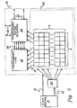
- FIG. 4 Shown in Fig. 4 is a diagram of FPGA 13 coupled to ROM 11.
- Each of the logic cells 19 includes the programming array of the present invention.
- the FPGA 13 reads configuration information into the programming arrays associated with the logic cells 19 as discussed above.
- a state machine 17 within FPGA 13 reads a parallel or sequential programming bit stream from ROM 11 that is disposed external to FPGA 13.
- the programming bit stream is appropriately directed to the programming words of the programming array of each logic cell 19 within the FPGA over data path 21.
- the state machine is coupled to the wordline of each programming word through, for example, conventional multiplexing circuitry such that each programming word may be loaded.
- the programming array maintains the ability to be reprogrammed in whole or in part, even during functional operation of the FPGA.
- Such reprogramming for the single programming word of conventional logic cells is available in some FPGAs and implementation thereof in connection with the present invention will be apparent to one of ordinary skill in the art.
- One example of such reconfiguration can be found in U.S. Patent number 5,336,950, entitled “CONFIGURATION FEATURES IN A CONFIGURABLE LOGIC ARRAY,” issued August 9, 1994 which is expressly incorporated herein by reference in its entirety.
- non-selected programming words of the array may be reprogrammed without any interruption in operation of the FPGA. Such reprogramming is performed by presenting data to be written on the write bitlines and latching the data into the desired programming word by engaging its write wordline.
- programmable counters 53 may be coupled to the programming arrays of the logic cells.
- a FPGA of the present invention can be implemented having a single, shared programmable counter 53 with its output coupled to the read wordlines of the logic cells.
- the FPGA functions conventionally, with the selected programming word for each logic cell determining the particular logic cell's configuration.
- the counter sequences in a preprogrammed manner through the address range of the programming array 50 of each logic cell, changing the logic cell's configuration.
- programming array 50 updates to provide a selected programming word to logic cell 19, thereby updating the logic cell's configuration.
- Data from the previous clock cycle is held undisturbed in logic cell latches (not shown) and is then processed against the new logic cell function and latched before the end of the new clock cycle. After that, the cell function is again updated by the programmable counter.
- the individual techniques for such latching will be apparent to one of ordinary skill in the art and are used in many different applications including, for example, other FPGAs and pipelined processors.
- programmable counters can be organized. There could be one programmable counter per column of logic cells ( Fig. 4 ), one programmable counter for the entire FPGA or any other useful organization of programmable counters. Of course, having more programmable counters per logic cell will provide greater operational flexibility, but at the expense of silicon real estate.
- the ability to dynamically change the programming of the logic cells in the FPGA as data passes therethrough facilitates the creation of many additional logic cell configurations. In this way, a few programmable logic cells can be used to emulate many fixed logic cells. A large virtual circuit density is thus created which more than accounts for the additional silicon real estate used by the programming arrays and programmable counters.
- the programming capability thereof provides, for example, the ability to:
- the programmable counter functions as a programmable state machine whose outputs control the address inputs to the programming arrays. Accordingly, with each change in state of the programmable counter, a corresponding programming word is coupled to the logic cell changing the configuration thereof.
- the counter itself may be implemented using dedicated logic, or even with programmed logic cells of the FPGA.
- portions of the array can be updated while not being accessed by the counter.
- the programming of the counter could be changed as well, or, in the case where multiple counters exist, the address connections from the programming array could be routed to a differently programmed counter.
- Many more such configuration variations are possible.
- the individual techniques required for such routing and configuration control are well known in the FPGA art and include, for example, multiplexing, transfer gates and tri-state circuits driven by programming word bits.
- each of the M programming words of the programming array 50 has a wordline 61.
- wordline 61 When a signal is asserted on the wordline of an individual programming word, that word is used to control the configuration of the logic cell 19.
- wordlines are programmably connected to the interconnect matrix within the FPGA such that connections thereto can be effected by logic cells therein (and external sources). This facilitates, for example, creating the programmable counter from logic cells of the FPGA as discussed hereinabove.
- Mask programming techniques include customizing the deposition of the final layers of metallization of an otherwise generally designed integrated circuit (see, for example, U.S. Patent No. 3,993,919 to Cox et al. entitled “PROGRAMMABLE LATCH AND OTHER CIRCUITS FOR LOGIC ARRAYS,” November 23, 1976; and U.S. Patent No. 4,742,383 to Fitzgerald entitled “MULTI-FUNCTION FET MASTERSLICE CELL,” May 3, 1988; both patents assigned to the same assignee as the present application).
- EPROM Erasable programmable read only memory
- EEPROM electrically erasable programmable read only memory
- EPROMS and EEPROMS are both electrically programmable and hold their states, even if power is removed. Special erase procedures can be used, however, to reconfigure the devices (see, for example, Wood et al., "AN ELECTRICALLY ALTERABLE PLA FOR FAST TURNAROUND TIME VLSI DEVELOPMENT HARDWARE," IEEE Journal of Solid-State Circuits, Vol. SC-16, No.
- RAM volatile random access memory
- SRAM memory cells programmed by a user.
- the SRAM memory cells can be configured in accordance with the techniques disclosed in the publication entitled “APPLICATION NOTE AT6000 SERIES CONFIGURATION", May 1993, Revision 1B, Atmel Corporation, which is hereby incorporated by reference in its entirety.
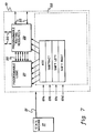
- a programmed logic cell 19 of an FPGA is shown in Fig. 7.
- the logic cell is programmed to perform one of four selectable math functions. Each of the four functions has been programmed into the logic cell by way of four selectable programming words. If wordline 61a is engaged, a programming word comprising the appropriate programming such that the cell performs an addition function is selected for logic cell 19. Similarly, engaging wordline 61b will effect a subtraction function in the cell while engaging wordlines 61c or 61d will effect a shift left or shift right function in the cell, respectively. In this example, the wordlines would be coupled to other logic cells in the FPGA that would select the appropriate wordline to engage the desired mathematical functions.
- the logic cell and its associated programming array are usable as a programmable core within other integrated circuits, such as, for example, an Application Specific Integrated Circuit ("ASIC") or a microprocessor.
- ASIC Application Specific Integrated Circuit
- the programmable core would comprise a programmable array as disclosed herein. Such a use would facilitate flexibility concerning reconfiguration for, and performance of, new computational tasks.
- the present invention has many advantages and features associated with it.
- the FPGA architecture disclosed resolves problems in both density and timing that are associated with data-flow based FPGA architectures.
- By providing alternate configurations of an array of logic cells many virtual logic cells are provided. This greatly enhances the functionality and capabilities of even a moderately sized array of logic cells.
- the reduction in actual physical logic cells needed to implement a function means that data spends more time resident in a single cell, and less time in transit between cells in the unpredictable timing environment of the inter-cell routing.
- the control-flow architecture of the present invention therefore yields significant timing improvements.
- the techniques of the present invention expand and enhance the capabilities of field programmable gate arrays.
Applications Claiming Priority (2)
| Application Number | Priority Date | Filing Date | Title |
|---|---|---|---|
| US462392 | 1995-06-05 | ||
| US08/462,392 US5646544A (en) | 1995-06-05 | 1995-06-05 | System and method for dynamically reconfiguring a programmable gate array |
Publications (2)
| Publication Number | Publication Date |
|---|---|
| EP0748051A2 true EP0748051A2 (fr) | 1996-12-11 |
| EP0748051A3 EP0748051A3 (fr) | 1997-12-17 |
Family
ID=23836277
Family Applications (1)
| Application Number | Title | Priority Date | Filing Date |
|---|---|---|---|
| EP96480061A Withdrawn EP0748051A3 (fr) | 1995-06-05 | 1996-05-07 | Système et procédé pour la reconfiguration dynamique d'un réseau de portes programmables |
Country Status (3)
| Country | Link |
|---|---|
| US (1) | US5646544A (fr) |
| EP (1) | EP0748051A3 (fr) |
| JP (1) | JPH08330945A (fr) |
Cited By (24)
| Publication number | Priority date | Publication date | Assignee | Title |
|---|---|---|---|---|
| WO1998029952A1 (fr) * | 1996-12-27 | 1998-07-09 | Pact Informationstechnologie Gmbh | Procede pour le transfert dynamique automatique de processeurs a flux de donnees (dfp) ainsi que de modules a deux ou plusieurs structures cellulaires programmables bidimensionnelles ou multidimensionnelles (epga, dpga ou analogues) |
| WO1998031102A1 (fr) * | 1996-12-20 | 1998-07-16 | Pact Informationstechnologie Gmbh | Procede de reconfiguration pour composants programmables pendant leur duree de fonctionnement |
| US5821776A (en) * | 1997-01-31 | 1998-10-13 | Actel Corporation | Field programmable gate array with mask programmed analog function circuits |
| WO1999034515A1 (fr) * | 1997-12-29 | 1999-07-08 | Advanced Micro Devices, Inc. | Memoire integree remanente electriquement effaçable et reprogrammable, avec fonctions de programmation et de verification dans le systeme (ispav) pour prendre en charge la reconfiguration dans le systeme d'unites logiques programmables |
| US6038650A (en) * | 1997-02-04 | 2000-03-14 | Pactgmbh | Method for the automatic address generation of modules within clusters comprised of a plurality of these modules |
| US6081903A (en) * | 1997-02-08 | 2000-06-27 | Pact Gmbh | Method of the self-synchronization of configurable elements of a programmable unit |
| GB2346240A (en) * | 1999-01-28 | 2000-08-02 | Nec Corp | Programmable device |
| US6119181A (en) * | 1996-12-20 | 2000-09-12 | Pact Gmbh | I/O and memory bus system for DFPs and units with two- or multi-dimensional programmable cell architectures |
| GB2350456A (en) * | 1999-05-13 | 2000-11-29 | Jpc Technology Ltd | Data processing |
| EP1198888A1 (fr) * | 1999-06-30 | 2002-04-24 | Chameleon Systems, Inc. | Systeme d'acces memoire et procede pour puce reconfigurable |
| US6405299B1 (en) | 1997-02-11 | 2002-06-11 | Pact Gmbh | Internal bus system for DFPS and units with two- or multi-dimensional programmable cell architectures, for managing large volumes of data with a high interconnection complexity |
| US6425068B1 (en) | 1996-12-09 | 2002-07-23 | Pact Gmbh | Unit for processing numeric and logic operations for use in central processing units (cpus), multiprocessor systems, data-flow processors (dsps), systolic processors and field programmable gate arrays (epgas) |
| US6480937B1 (en) | 1998-02-25 | 2002-11-12 | Pact Informationstechnologie Gmbh | Method for hierarchical caching of configuration data having dataflow processors and modules having two-or multidimensional programmable cell structure (FPGAs, DPGAs, etc.)-- |
| EP1329816A2 (fr) * | 1996-12-27 | 2003-07-23 | Pact Informationstechnologie GmbH | Procédé pour le transfert dynamique automatique de processeurs à flux de données (dfp) ainsi que de modules à deux ou plusieurs structures cellulaires programmables bidimensionnelles ou multidimensionnelles (fpga, dpga ou analogues) |
| US6859869B1 (en) | 1995-11-17 | 2005-02-22 | Pact Xpp Technologies Ag | Data processing system |
| WO2005111842A1 (fr) * | 2004-04-30 | 2005-11-24 | Xilinx, Inc. | Reconfigration dynamique |
| US7109750B2 (en) | 2004-04-30 | 2006-09-19 | Xilinx, Inc. | Reconfiguration port for dynamic reconfiguration-controller |
| US7126372B2 (en) | 2004-04-30 | 2006-10-24 | Xilinx, Inc. | Reconfiguration port for dynamic reconfiguration—sub-frame access for reconfiguration |
| US7218137B2 (en) | 2004-04-30 | 2007-05-15 | Xilinx, Inc. | Reconfiguration port for dynamic reconfiguration |
| US7233532B2 (en) | 2004-04-30 | 2007-06-19 | Xilinx, Inc. | Reconfiguration port for dynamic reconfiguration-system monitor interface |
| USRE44365E1 (en) | 1997-02-08 | 2013-07-09 | Martin Vorbach | Method of self-synchronization of configurable elements of a programmable module |
| US9037807B2 (en) | 2001-03-05 | 2015-05-19 | Pact Xpp Technologies Ag | Processor arrangement on a chip including data processing, memory, and interface elements |
| US9047440B2 (en) | 2000-10-06 | 2015-06-02 | Pact Xpp Technologies Ag | Logical cell array and bus system |
| US9075605B2 (en) | 2001-03-05 | 2015-07-07 | Pact Xpp Technologies Ag | Methods and devices for treating and processing data |
Families Citing this family (182)
| Publication number | Priority date | Publication date | Assignee | Title |
|---|---|---|---|---|
| US5367208A (en) | 1986-09-19 | 1994-11-22 | Actel Corporation | Reconfigurable programmable interconnect architecture |
| JPH09231788A (ja) * | 1995-12-19 | 1997-09-05 | Fujitsu Ltd | シフトレジスタ及びプログラマブル論理回路並びにプログラマブル論理回路システム |
| US7266725B2 (en) | 2001-09-03 | 2007-09-04 | Pact Xpp Technologies Ag | Method for debugging reconfigurable architectures |
| WO2002029600A2 (fr) * | 2000-10-06 | 2002-04-11 | Pact Informationstechnologie Gmbh | Procede et dispositif |
| US6020758A (en) * | 1996-03-11 | 2000-02-01 | Altera Corporation | Partially reconfigurable programmable logic device |
| US5784636A (en) * | 1996-05-28 | 1998-07-21 | National Semiconductor Corporation | Reconfigurable computer architecture for use in signal processing applications |
| JP2000513523A (ja) * | 1996-06-21 | 2000-10-10 | オーガニック システムズ インコーポレイテッド | プロセスの即時制御を行う動的に再構成可能なハードウェアシステム |
| US5838165A (en) * | 1996-08-21 | 1998-11-17 | Chatter; Mukesh | High performance self modifying on-the-fly alterable logic FPGA, architecture and method |
| US6338106B1 (en) | 1996-12-20 | 2002-01-08 | Pact Gmbh | I/O and memory bus system for DFPS and units with two or multi-dimensional programmable cell architectures |
| US5959466A (en) | 1997-01-31 | 1999-09-28 | Actel Corporation | Field programmable gate array with mask programmed input and output buffers |
| US6150837A (en) | 1997-02-28 | 2000-11-21 | Actel Corporation | Enhanced field programmable gate array |
| JP3106998B2 (ja) | 1997-04-11 | 2000-11-06 | 日本電気株式会社 | メモリ付加型プログラマブルロジックlsi |
| US6011407A (en) * | 1997-06-13 | 2000-01-04 | Xilinx, Inc. | Field programmable gate array with dedicated computer bus interface and method for configuring both |
| US9092595B2 (en) | 1997-10-08 | 2015-07-28 | Pact Xpp Technologies Ag | Multiprocessor having associated RAM units |
| US8686549B2 (en) | 2001-09-03 | 2014-04-01 | Martin Vorbach | Reconfigurable elements |
| DE19861088A1 (de) | 1997-12-22 | 2000-02-10 | Pact Inf Tech Gmbh | Verfahren zur Reparatur von integrierten Schaltkreisen |
| US6198303B1 (en) * | 1998-03-25 | 2001-03-06 | Altera Corporation | Configuration eprom with programmable logic |
| WO2002013000A2 (fr) | 2000-06-13 | 2002-02-14 | Pact Informationstechnologie Gmbh | Protocoles et communication d'unites de configuration de pipeline |
| AU5805300A (en) | 1999-06-10 | 2001-01-02 | Pact Informationstechnologie Gmbh | Sequence partitioning in cell structures |
| JP3520810B2 (ja) | 1999-07-02 | 2004-04-19 | 日本電気株式会社 | バックアップ機能を有するデータ保持回路 |
| GB2352548B (en) * | 1999-07-26 | 2001-06-06 | Sun Microsystems Inc | Method and apparatus for executing standard functions in a computer system |
| US8160864B1 (en) | 2000-10-26 | 2012-04-17 | Cypress Semiconductor Corporation | In-circuit emulator and pod synchronized boot |
| US6724220B1 (en) | 2000-10-26 | 2004-04-20 | Cyress Semiconductor Corporation | Programmable microcontroller architecture (mixed analog/digital) |
| US8103496B1 (en) | 2000-10-26 | 2012-01-24 | Cypress Semicondutor Corporation | Breakpoint control in an in-circuit emulation system |
| US8176296B2 (en) | 2000-10-26 | 2012-05-08 | Cypress Semiconductor Corporation | Programmable microcontroller architecture |
| US8149048B1 (en) | 2000-10-26 | 2012-04-03 | Cypress Semiconductor Corporation | Apparatus and method for programmable power management in a programmable analog circuit block |
| US7765095B1 (en) | 2000-10-26 | 2010-07-27 | Cypress Semiconductor Corporation | Conditional branching in an in-circuit emulation system |
| US9250908B2 (en) | 2001-03-05 | 2016-02-02 | Pact Xpp Technologies Ag | Multi-processor bus and cache interconnection system |
| US7581076B2 (en) * | 2001-03-05 | 2009-08-25 | Pact Xpp Technologies Ag | Methods and devices for treating and/or processing data |
| US7844796B2 (en) | 2001-03-05 | 2010-11-30 | Martin Vorbach | Data processing device and method |
| US9552047B2 (en) | 2001-03-05 | 2017-01-24 | Pact Xpp Technologies Ag | Multiprocessor having runtime adjustable clock and clock dependent power supply |
| US9436631B2 (en) | 2001-03-05 | 2016-09-06 | Pact Xpp Technologies Ag | Chip including memory element storing higher level memory data on a page by page basis |
| US9141390B2 (en) | 2001-03-05 | 2015-09-22 | Pact Xpp Technologies Ag | Method of processing data with an array of data processors according to application ID |
| US7752419B1 (en) | 2001-03-22 | 2010-07-06 | Qst Holdings, Llc | Method and system for managing hardware resources to implement system functions using an adaptive computing architecture |
| US7624204B2 (en) * | 2001-03-22 | 2009-11-24 | Nvidia Corporation | Input/output controller node in an adaptable computing environment |
| US6836839B2 (en) | 2001-03-22 | 2004-12-28 | Quicksilver Technology, Inc. | Adaptive integrated circuitry with heterogeneous and reconfigurable matrices of diverse and adaptive computational units having fixed, application specific computational elements |
| US7962716B2 (en) | 2001-03-22 | 2011-06-14 | Qst Holdings, Inc. | Adaptive integrated circuitry with heterogeneous and reconfigurable matrices of diverse and adaptive computational units having fixed, application specific computational elements |
| US7325123B2 (en) * | 2001-03-22 | 2008-01-29 | Qst Holdings, Llc | Hierarchical interconnect for configuring separate interconnects for each group of fixed and diverse computational elements |
| US7433909B2 (en) | 2002-06-25 | 2008-10-07 | Nvidia Corporation | Processing architecture for a reconfigurable arithmetic node |
| US7653710B2 (en) | 2002-06-25 | 2010-01-26 | Qst Holdings, Llc. | Hardware task manager |
| US7249242B2 (en) | 2002-10-28 | 2007-07-24 | Nvidia Corporation | Input pipeline registers for a node in an adaptive computing engine |
| US7489779B2 (en) * | 2001-03-22 | 2009-02-10 | Qstholdings, Llc | Hardware implementation of the secure hash standard |
| US6577678B2 (en) | 2001-05-08 | 2003-06-10 | Quicksilver Technology | Method and system for reconfigurable channel coding |
| US6618434B2 (en) * | 2001-05-31 | 2003-09-09 | Quicksilver Technology, Inc. | Adaptive, multimode rake receiver for dynamic search and multipath reception |
| US10031733B2 (en) | 2001-06-20 | 2018-07-24 | Scientia Sol Mentis Ag | Method for processing data |
| EP2224330B1 (fr) | 2001-06-20 | 2012-05-09 | Krass, Maren | Procede et systeme pour decouper des logiciels volumineux |
| US7996827B2 (en) | 2001-08-16 | 2011-08-09 | Martin Vorbach | Method for the translation of programs for reconfigurable architectures |
| US7434191B2 (en) | 2001-09-03 | 2008-10-07 | Pact Xpp Technologies Ag | Router |
| US8686475B2 (en) | 2001-09-19 | 2014-04-01 | Pact Xpp Technologies Ag | Reconfigurable elements |
| US7420392B2 (en) | 2001-09-28 | 2008-09-02 | Xilinx, Inc. | Programmable gate array and embedded circuitry initialization and processing |
| US7406674B1 (en) | 2001-10-24 | 2008-07-29 | Cypress Semiconductor Corporation | Method and apparatus for generating microcontroller configuration information |
| US8078970B1 (en) | 2001-11-09 | 2011-12-13 | Cypress Semiconductor Corporation | Graphical user interface with user-selectable list-box |
| US8042093B1 (en) | 2001-11-15 | 2011-10-18 | Cypress Semiconductor Corporation | System providing automatic source code generation for personalization and parameterization of user modules |
| US6971004B1 (en) | 2001-11-19 | 2005-11-29 | Cypress Semiconductor Corp. | System and method of dynamically reconfiguring a programmable integrated circuit |
| US7774190B1 (en) | 2001-11-19 | 2010-08-10 | Cypress Semiconductor Corporation | Sleep and stall in an in-circuit emulation system |
| US8069405B1 (en) | 2001-11-19 | 2011-11-29 | Cypress Semiconductor Corporation | User interface for efficiently browsing an electronic document using data-driven tabs |
| US7770113B1 (en) | 2001-11-19 | 2010-08-03 | Cypress Semiconductor Corporation | System and method for dynamically generating a configuration datasheet |
| US7844437B1 (en) | 2001-11-19 | 2010-11-30 | Cypress Semiconductor Corporation | System and method for performing next placements and pruning of disallowed placements for programming an integrated circuit |
| US7046635B2 (en) | 2001-11-28 | 2006-05-16 | Quicksilver Technology, Inc. | System for authorizing functionality in adaptable hardware devices |
| US6986021B2 (en) | 2001-11-30 | 2006-01-10 | Quick Silver Technology, Inc. | Apparatus, method, system and executable module for configuration and operation of adaptive integrated circuitry having fixed, application specific computational elements |
| US8412915B2 (en) * | 2001-11-30 | 2013-04-02 | Altera Corporation | Apparatus, system and method for configuration of adaptive integrated circuitry having heterogeneous computational elements |
| US7644279B2 (en) * | 2001-12-05 | 2010-01-05 | Nvidia Corporation | Consumer product distribution in the embedded system market |
| US7215701B2 (en) | 2001-12-12 | 2007-05-08 | Sharad Sambhwani | Low I/O bandwidth method and system for implementing detection and identification of scrambling codes |
| US7403981B2 (en) | 2002-01-04 | 2008-07-22 | Quicksilver Technology, Inc. | Apparatus and method for adaptive multimedia reception and transmission in communication environments |
| WO2003060747A2 (fr) | 2002-01-19 | 2003-07-24 | Pact Xpp Technologies Ag | Processeur reconfigurable |
| US8127061B2 (en) | 2002-02-18 | 2012-02-28 | Martin Vorbach | Bus systems and reconfiguration methods |
| US8914590B2 (en) | 2002-08-07 | 2014-12-16 | Pact Xpp Technologies Ag | Data processing method and device |
| US9170812B2 (en) | 2002-03-21 | 2015-10-27 | Pact Xpp Technologies Ag | Data processing system having integrated pipelined array data processor |
| US8103497B1 (en) | 2002-03-28 | 2012-01-24 | Cypress Semiconductor Corporation | External interface for event architecture |
| US6732354B2 (en) * | 2002-04-23 | 2004-05-04 | Quicksilver Technology, Inc. | Method, system and software for programming reconfigurable hardware |
| US7308608B1 (en) | 2002-05-01 | 2007-12-11 | Cypress Semiconductor Corporation | Reconfigurable testing system and method |
| US7328414B1 (en) | 2003-05-13 | 2008-02-05 | Qst Holdings, Llc | Method and system for creating and programming an adaptive computing engine |
| US7660984B1 (en) | 2003-05-13 | 2010-02-09 | Quicksilver Technology | Method and system for achieving individualized protected space in an operating system |
| US7620678B1 (en) | 2002-06-12 | 2009-11-17 | Nvidia Corporation | Method and system for reducing the time-to-market concerns for embedded system design |
| US20040133709A1 (en) * | 2002-07-09 | 2004-07-08 | International Business Machines Corporation | Method and system for personalized I/O device initialization |
| US7802108B1 (en) | 2002-07-18 | 2010-09-21 | Nvidia Corporation | Secure storage of program code for an embedded system |
| AU2003286131A1 (en) | 2002-08-07 | 2004-03-19 | Pact Xpp Technologies Ag | Method and device for processing data |
| US7657861B2 (en) | 2002-08-07 | 2010-02-02 | Pact Xpp Technologies Ag | Method and device for processing data |
| US8108656B2 (en) | 2002-08-29 | 2012-01-31 | Qst Holdings, Llc | Task definition for specifying resource requirements |
| WO2004038599A1 (fr) | 2002-09-06 | 2004-05-06 | Pact Xpp Technologies Ag | Structure de sequenceur reconfigurable |
| US7761845B1 (en) | 2002-09-09 | 2010-07-20 | Cypress Semiconductor Corporation | Method for parameterizing a user module |
| US6803787B1 (en) * | 2002-09-25 | 2004-10-12 | Lattice Semiconductor Corp. | State machine in a programmable logic device |
| US7502915B2 (en) * | 2002-09-30 | 2009-03-10 | Nvidia Corporation | System and method using embedded microprocessor as a node in an adaptable computing machine |
| US7937591B1 (en) | 2002-10-25 | 2011-05-03 | Qst Holdings, Llc | Method and system for providing a device which can be adapted on an ongoing basis |
| US8949576B2 (en) * | 2002-11-01 | 2015-02-03 | Nvidia Corporation | Arithmetic node including general digital signal processing functions for an adaptive computing machine |
| US8276135B2 (en) | 2002-11-07 | 2012-09-25 | Qst Holdings Llc | Profiling of software and circuit designs utilizing data operation analyses |
| US7225301B2 (en) | 2002-11-22 | 2007-05-29 | Quicksilver Technologies | External memory controller node |
| US8296764B2 (en) | 2003-08-14 | 2012-10-23 | Nvidia Corporation | Internal synchronization control for adaptive integrated circuitry |
| US7174432B2 (en) | 2003-08-19 | 2007-02-06 | Nvidia Corporation | Asynchronous, independent and multiple process shared memory system in an adaptive computing architecture |
| JP4700611B2 (ja) | 2003-08-28 | 2011-06-15 | ペーアーツェーテー イクスペーペー テクノロジーズ アクチエンゲゼルシャフト | データ処理装置およびデータ処理方法 |
| US7126373B1 (en) | 2004-02-14 | 2006-10-24 | Herman Schmit | Configurable logic circuits with commutative properties |
| US7193440B1 (en) * | 2004-02-14 | 2007-03-20 | Herman Schmit | Configurable circuits, IC's, and systems |
| US7109752B1 (en) * | 2004-02-14 | 2006-09-19 | Herman Schmit | Configurable circuits, IC's, and systems |
| US7284222B1 (en) * | 2004-06-30 | 2007-10-16 | Tabula, Inc. | Method and apparatus for identifying connections between configurable nodes in a configurable integrated circuit |
| US7167025B1 (en) * | 2004-02-14 | 2007-01-23 | Herman Schmit | Non-sequentially configurable IC |
| US7425841B2 (en) | 2004-02-14 | 2008-09-16 | Tabula Inc. | Configurable circuits, IC's, and systems |
| US7157933B1 (en) | 2004-02-14 | 2007-01-02 | Herman Schmit | Configurable circuits, IC's, and systems |
| US7193432B1 (en) | 2004-02-14 | 2007-03-20 | Herman Schmit | VPA logic circuits |
| US7126381B1 (en) | 2004-02-14 | 2006-10-24 | Herman Schmit | VPA interconnect circuit |
| US7295049B1 (en) | 2004-03-25 | 2007-11-13 | Cypress Semiconductor Corporation | Method and circuit for rapid alignment of signals |
| JP2006011825A (ja) * | 2004-06-25 | 2006-01-12 | Fujitsu Ltd | 再構成可能演算装置および半導体装置 |
| US7282950B1 (en) | 2004-11-08 | 2007-10-16 | Tabula, Inc. | Configurable IC's with logic resources with offset connections |
| US7449915B2 (en) * | 2004-06-30 | 2008-11-11 | Tabula Inc. | VPA logic circuits |
| US7408382B2 (en) * | 2004-06-30 | 2008-08-05 | Tabula, Inc. | Configurable circuits, IC's, and systems |
| US7193438B1 (en) | 2004-06-30 | 2007-03-20 | Andre Rohe | Configurable integrated circuit with offset connection |
| US7439766B2 (en) * | 2004-06-30 | 2008-10-21 | Tabula, Inc. | Configurable logic circuits with commutative properties |
| US7312630B2 (en) * | 2004-06-30 | 2007-12-25 | Tabula, Inc. | Configurable integrated circuit with built-in turns |
| US7145361B1 (en) | 2004-06-30 | 2006-12-05 | Andre Rohe | Configurable integrated circuit with different connection schemes |
| CN100545827C (zh) | 2004-07-30 | 2009-09-30 | 富士通株式会社 | 可重配置电路及可重配置电路的控制方法 |
| US8069436B2 (en) | 2004-08-13 | 2011-11-29 | Cypress Semiconductor Corporation | Providing hardware independence to automate code generation of processing device firmware |
| US7317331B2 (en) | 2004-11-08 | 2008-01-08 | Tabula, Inc. | Reconfigurable IC that has sections running at different reconfiguration rates |
| US7917559B2 (en) * | 2004-11-08 | 2011-03-29 | Tabula, Inc. | Configurable IC's with configurable logic circuits that perform adder and/or subtractor operations |
| US7743085B2 (en) * | 2004-11-08 | 2010-06-22 | Tabula, Inc. | Configurable IC with large carry chains |
| US7573296B2 (en) | 2004-11-08 | 2009-08-11 | Tabula Inc. | Configurable IC with configurable routing resources that have asymmetric input and/or outputs |
| US7268586B1 (en) | 2004-11-08 | 2007-09-11 | Tabula, Inc. | Method and apparatus for accessing stored data in a reconfigurable IC |
| US7342415B2 (en) * | 2004-11-08 | 2008-03-11 | Tabula, Inc. | Configurable IC with interconnect circuits that also perform storage operations |
| US7242216B1 (en) | 2004-11-08 | 2007-07-10 | Herman Schmit | Embedding memory between tile arrangement of a configurable IC |
| US7224181B1 (en) * | 2004-11-08 | 2007-05-29 | Herman Schmit | Clock distribution in a configurable IC |
| US7259587B1 (en) | 2004-11-08 | 2007-08-21 | Tabula, Inc. | Configurable IC's with configurable logic resources that have asymetric inputs and/or outputs |
| US7301368B2 (en) | 2005-03-15 | 2007-11-27 | Tabula, Inc. | Embedding memory within tile arrangement of a configurable IC |
| US7276933B1 (en) * | 2004-11-08 | 2007-10-02 | Tabula, Inc. | Reconfigurable IC that has sections running at different looperness |
| US7295037B2 (en) * | 2004-11-08 | 2007-11-13 | Tabula, Inc. | Configurable IC with routing circuits with offset connections |
| US7330050B2 (en) | 2004-11-08 | 2008-02-12 | Tabula, Inc. | Storage elements for a configurable IC and method and apparatus for accessing data stored in the storage elements |
| US20070244958A1 (en) * | 2004-11-08 | 2007-10-18 | Jason Redgrave | Configurable IC's with carry bypass circuitry |
| US7496879B2 (en) * | 2004-12-01 | 2009-02-24 | Tabula, Inc. | Concurrent optimization of physical design and operational cycle assignment |
| US7236009B1 (en) | 2004-12-01 | 2007-06-26 | Andre Rohe | Operational time extension |
| US7428721B2 (en) * | 2004-12-01 | 2008-09-23 | Tabula, Inc. | Operational cycle assignment in a configurable IC |
| JP2006186774A (ja) * | 2004-12-28 | 2006-07-13 | Hitachi Ltd | 半導体集積装置、それを用いた電子機器、および、その使用に関する課金方法 |
| US7332976B1 (en) | 2005-02-04 | 2008-02-19 | Cypress Semiconductor Corporation | Poly-phase frequency synthesis oscillator |
| US7224182B1 (en) * | 2005-03-15 | 2007-05-29 | Brad Hutchings | Hybrid configurable circuit for a configurable IC |
| US7530033B2 (en) | 2005-03-15 | 2009-05-05 | Tabula, Inc. | Method and apparatus for decomposing functions in a configurable IC |
| US7230869B1 (en) | 2005-03-15 | 2007-06-12 | Jason Redgrave | Method and apparatus for accessing contents of memory cells |
| US20070244959A1 (en) * | 2005-03-15 | 2007-10-18 | Steven Teig | Configurable IC's with dual carry chains |
| US7310003B2 (en) * | 2005-03-15 | 2007-12-18 | Tabula, Inc. | Configurable IC with interconnect circuits that have select lines driven by user signals |
| US7298169B2 (en) * | 2005-03-15 | 2007-11-20 | Tabula, Inc | Hybrid logic/interconnect circuit in a configurable IC |
| US7825684B2 (en) * | 2005-03-15 | 2010-11-02 | Tabula, Inc. | Variable width management for a memory of a configurable IC |
| US7400183B1 (en) | 2005-05-05 | 2008-07-15 | Cypress Semiconductor Corporation | Voltage controlled oscillator delay cell and method |
| JP4720436B2 (ja) * | 2005-11-01 | 2011-07-13 | 株式会社日立製作所 | リコンフィギュラブルプロセッサまたは装置 |
| US7818361B1 (en) | 2005-11-07 | 2010-10-19 | Tabula, Inc. | Method and apparatus for performing two's complement multiplication |
| US7765249B1 (en) | 2005-11-07 | 2010-07-27 | Tabula, Inc. | Use of hybrid interconnect/logic circuits for multiplication |
| US7372297B1 (en) | 2005-11-07 | 2008-05-13 | Tabula Inc. | Hybrid interconnect/logic circuits enabling efficient replication of a function in several sub-cycles to save logic and routing resources |
| US8463836B1 (en) | 2005-11-07 | 2013-06-11 | Tabula, Inc. | Performing mathematical and logical operations in multiple sub-cycles |
| US7489162B1 (en) | 2005-12-01 | 2009-02-10 | Tabula, Inc. | Users registers in a reconfigurable IC |
| US7679401B1 (en) * | 2005-12-01 | 2010-03-16 | Tabula, Inc. | User registers implemented with routing circuits in a configurable IC |
| US7461362B1 (en) | 2005-12-01 | 2008-12-02 | Tabula, Inc. | Replacing circuit design elements with their equivalents |
| US8085067B1 (en) | 2005-12-21 | 2011-12-27 | Cypress Semiconductor Corporation | Differential-to-single ended signal converter circuit and method |
| EP1974265A1 (fr) | 2006-01-18 | 2008-10-01 | PACT XPP Technologies AG | Procédé de définition de matériels |
| US7797497B1 (en) | 2006-03-08 | 2010-09-14 | Tabula, Inc. | System and method for providing more logical memory ports than physical memory ports |
| US7609085B1 (en) | 2006-03-08 | 2009-10-27 | Tabula, Inc. | Configurable integrated circuit with a 4-to-1 multiplexer |
| US7518400B1 (en) | 2006-03-08 | 2009-04-14 | Tabula, Inc. | Barrel shifter implemented on a configurable integrated circuit |
| US7504858B1 (en) | 2006-03-08 | 2009-03-17 | Tabula, Inc. | Configurable integrated circuit with parallel non-neighboring offset connections |
| US7694083B1 (en) | 2006-03-08 | 2010-04-06 | Tabula, Inc. | System and method for providing a virtual memory architecture narrower and deeper than a physical memory architecture |
| US7529992B1 (en) | 2006-03-27 | 2009-05-05 | Tabula, Inc. | Configurable integrated circuit with error correcting circuitry |
| US8067948B2 (en) | 2006-03-27 | 2011-11-29 | Cypress Semiconductor Corporation | Input/output multiplexer bus |
| US7669097B1 (en) | 2006-03-27 | 2010-02-23 | Tabula, Inc. | Configurable IC with error detection and correction circuitry |
| US7930666B1 (en) | 2006-12-12 | 2011-04-19 | Tabula, Inc. | System and method of providing a memory hierarchy |
| US7587697B1 (en) | 2006-12-12 | 2009-09-08 | Tabula, Inc. | System and method of mapping memory blocks in a configurable integrated circuit |
| EP2140548A4 (fr) * | 2007-03-20 | 2010-06-09 | Tabula Inc | Ci configurable possédant un tissu de routage avec des éléments de stockage |
| US8112468B1 (en) | 2007-03-22 | 2012-02-07 | Tabula, Inc. | Method and apparatus for performing an operation with a plurality of sub-operations in a configurable IC |
| US8092083B2 (en) | 2007-04-17 | 2012-01-10 | Cypress Semiconductor Corporation | Temperature sensor with digital bandgap |
| US7987065B1 (en) | 2007-04-17 | 2011-07-26 | Nvidia Corporation | Automatic quality testing of multimedia rendering by software drivers |
| US8130025B2 (en) | 2007-04-17 | 2012-03-06 | Cypress Semiconductor Corporation | Numerical band gap |
| US7737724B2 (en) | 2007-04-17 | 2010-06-15 | Cypress Semiconductor Corporation | Universal digital block interconnection and channel routing |
| US8026739B2 (en) | 2007-04-17 | 2011-09-27 | Cypress Semiconductor Corporation | System level interconnect with programmable switching |
| US8040266B2 (en) | 2007-04-17 | 2011-10-18 | Cypress Semiconductor Corporation | Programmable sigma-delta analog-to-digital converter |
| US9564902B2 (en) | 2007-04-17 | 2017-02-07 | Cypress Semiconductor Corporation | Dynamically configurable and re-configurable data path |
| US8516025B2 (en) | 2007-04-17 | 2013-08-20 | Cypress Semiconductor Corporation | Clock driven dynamic datapath chaining |
| US8266575B1 (en) | 2007-04-25 | 2012-09-11 | Cypress Semiconductor Corporation | Systems and methods for dynamically reconfiguring a programmable system on a chip |
| US8065653B1 (en) | 2007-04-25 | 2011-11-22 | Cypress Semiconductor Corporation | Configuration of programmable IC design elements |
| US9720805B1 (en) | 2007-04-25 | 2017-08-01 | Cypress Semiconductor Corporation | System and method for controlling a target device |
| US8049569B1 (en) | 2007-09-05 | 2011-11-01 | Cypress Semiconductor Corporation | Circuit and method for improving the accuracy of a crystal-less oscillator having dual-frequency modes |
| EP2201569A4 (fr) | 2007-09-06 | 2011-07-13 | Tabula Inc | Commutateur de contexte de configuration |
| US8863067B1 (en) | 2008-02-06 | 2014-10-14 | Tabula, Inc. | Sequential delay analysis by placement engines |
| GB2457912A (en) * | 2008-02-27 | 2009-09-02 | Silicon Basis Ltd | An FPGA which is reconfigured between each clock cycle |
| US8166435B2 (en) | 2008-06-26 | 2012-04-24 | Tabula, Inc. | Timing operations in an IC with configurable circuits |
| WO2010033263A1 (fr) | 2008-09-17 | 2010-03-25 | Tabula, Inc. | Éléments de stockage contrôlables pour un circuit intégré |
| US9448964B2 (en) | 2009-05-04 | 2016-09-20 | Cypress Semiconductor Corporation | Autonomous control in a programmable system |
| JP5990466B2 (ja) | 2010-01-21 | 2016-09-14 | スビラル・インコーポレーテッド | ストリームに基づく演算を実装するための汎用複数コアシステムのための方法および装置 |
| WO2011123151A1 (fr) | 2010-04-02 | 2011-10-06 | Tabula Inc. | Système et procédé de réduction de la consommation d'énergie lors d'une reconfiguration |
| US9455715B2 (en) | 2011-06-30 | 2016-09-27 | Alterm Corporation | Apparatus for improving reliability of electronic circuitry and associated methods |
| US8941409B2 (en) | 2011-07-01 | 2015-01-27 | Tabula, Inc. | Configurable storage elements |
| JP6228381B2 (ja) * | 2012-04-30 | 2017-11-08 | 株式会社半導体エネルギー研究所 | 半導体装置 |
Citations (6)
| Publication number | Priority date | Publication date | Assignee | Title |
|---|---|---|---|---|
| US4374412A (en) * | 1965-05-25 | 1983-02-15 | Schaffner Mario R | Circulating page loose system |
| DE3821515A1 (de) * | 1988-06-25 | 1989-12-28 | Rico Mikroelektronik Gmbh | Programmierbare gatteranordnung |
| WO1994001867A1 (fr) * | 1992-07-02 | 1994-01-20 | Camarota Rafael C | Systeme a memoire adressable selectivement non interruptif |
| WO1994014123A1 (fr) * | 1992-12-11 | 1994-06-23 | National Technology, Inc. | Dispositif de calcul a circuit integre comprenant des circuits prediffuses configurables dynamiquement a microprocesseur et un systeme d'execution d'instructions reconfigurable |
| US5336950A (en) * | 1991-08-29 | 1994-08-09 | National Semiconductor Corporation | Configuration features in a configurable logic array |
| EP0678985A2 (fr) * | 1994-04-20 | 1995-10-25 | Xilinx, Inc. | Dispositif logique programmable qui mémorise plus d'une configuration et un moyen pour commuter des configurations |
Family Cites Families (16)
| Publication number | Priority date | Publication date | Assignee | Title |
|---|---|---|---|---|
| US4870302A (en) * | 1984-03-12 | 1989-09-26 | Xilinx, Inc. | Configurable electrical circuit having configurable logic elements and configurable interconnects |
| USRE34363E (en) * | 1984-03-12 | 1993-08-31 | Xilinx, Inc. | Configurable electrical circuit having configurable logic elements and configurable interconnects |
| US4700187A (en) * | 1985-12-02 | 1987-10-13 | Concurrent Logic, Inc. | Programmable, asynchronous logic cell and array |
| US4845633A (en) * | 1985-12-02 | 1989-07-04 | Apple Computer Inc. | System for programming graphically a programmable, asynchronous logic cell and array |
| US5019736A (en) * | 1986-11-07 | 1991-05-28 | Concurrent Logic, Inc. | Programmable logic cell and array |
| US4918440A (en) * | 1986-11-07 | 1990-04-17 | Furtek Frederick C | Programmable logic cell and array |
| US5089973A (en) * | 1986-11-07 | 1992-02-18 | Apple Computer Inc. | Programmable logic cell and array |
| US5155389A (en) * | 1986-11-07 | 1992-10-13 | Concurrent Logic, Inc. | Programmable logic cell and array |
| US5144166A (en) * | 1990-11-02 | 1992-09-01 | Concurrent Logic, Inc. | Programmable logic cell and array |
| US5313119A (en) * | 1991-03-18 | 1994-05-17 | Crosspoint Solutions, Inc. | Field programmable gate array |
| US5239510A (en) * | 1991-11-25 | 1993-08-24 | At&T Bell Laboratories | Multiple voltage supplies for field programmable gate arrays and the like |
| US5347519A (en) * | 1991-12-03 | 1994-09-13 | Crosspoint Solutions Inc. | Preprogramming testing in a field programmable gate array |
| US5208491A (en) * | 1992-01-07 | 1993-05-04 | Washington Research Foundation | Field programmable gate array |
| US5365125A (en) * | 1992-07-23 | 1994-11-15 | Xilinx, Inc. | Logic cell for field programmable gate array having optional internal feedback and optional cascade |
| KR960003373B1 (ko) * | 1992-09-29 | 1996-03-09 | 후지쓰 가부시키가이샤 | 프로그래머블 논리회로 |
| US5465056A (en) * | 1994-06-30 | 1995-11-07 | I-Cube, Inc. | Apparatus for programmable circuit and signal switching |
-
1995
- 1995-06-05 US US08/462,392 patent/US5646544A/en not_active Expired - Fee Related
-
1996
- 1996-05-07 EP EP96480061A patent/EP0748051A3/fr not_active Withdrawn
- 1996-05-15 JP JP8120547A patent/JPH08330945A/ja active Pending
Patent Citations (6)
| Publication number | Priority date | Publication date | Assignee | Title |
|---|---|---|---|---|
| US4374412A (en) * | 1965-05-25 | 1983-02-15 | Schaffner Mario R | Circulating page loose system |
| DE3821515A1 (de) * | 1988-06-25 | 1989-12-28 | Rico Mikroelektronik Gmbh | Programmierbare gatteranordnung |
| US5336950A (en) * | 1991-08-29 | 1994-08-09 | National Semiconductor Corporation | Configuration features in a configurable logic array |
| WO1994001867A1 (fr) * | 1992-07-02 | 1994-01-20 | Camarota Rafael C | Systeme a memoire adressable selectivement non interruptif |
| WO1994014123A1 (fr) * | 1992-12-11 | 1994-06-23 | National Technology, Inc. | Dispositif de calcul a circuit integre comprenant des circuits prediffuses configurables dynamiquement a microprocesseur et un systeme d'execution d'instructions reconfigurable |
| EP0678985A2 (fr) * | 1994-04-20 | 1995-10-25 | Xilinx, Inc. | Dispositif logique programmable qui mémorise plus d'une configuration et un moyen pour commuter des configurations |
Cited By (38)
| Publication number | Priority date | Publication date | Assignee | Title |
|---|---|---|---|---|
| US6859869B1 (en) | 1995-11-17 | 2005-02-22 | Pact Xpp Technologies Ag | Data processing system |
| US6425068B1 (en) | 1996-12-09 | 2002-07-23 | Pact Gmbh | Unit for processing numeric and logic operations for use in central processing units (cpus), multiprocessor systems, data-flow processors (dsps), systolic processors and field programmable gate arrays (epgas) |
| US6728871B1 (en) | 1996-12-09 | 2004-04-27 | Pact Xpp Technologies Ag | Runtime configurable arithmetic and logic cell |
| US6119181A (en) * | 1996-12-20 | 2000-09-12 | Pact Gmbh | I/O and memory bus system for DFPs and units with two- or multi-dimensional programmable cell architectures |
| US6021490A (en) * | 1996-12-20 | 2000-02-01 | Pact Gmbh | Run-time reconfiguration method for programmable units |
| WO1998031102A1 (fr) * | 1996-12-20 | 1998-07-16 | Pact Informationstechnologie Gmbh | Procede de reconfiguration pour composants programmables pendant leur duree de fonctionnement |
| EP1146432A3 (fr) * | 1996-12-20 | 2005-03-30 | PACT XPP Technologies AG | Procédé de reconfiguration pour composants programmables pendant leur durée de fonctionnement |
| EP1146432A2 (fr) | 1996-12-20 | 2001-10-17 | Pact Informationstechnologie GmbH | Procédé de reconfiguration pour composants programmables pendant leur durée de fonctionnement |
| EP1329816A2 (fr) * | 1996-12-27 | 2003-07-23 | Pact Informationstechnologie GmbH | Procédé pour le transfert dynamique automatique de processeurs à flux de données (dfp) ainsi que de modules à deux ou plusieurs structures cellulaires programmables bidimensionnelles ou multidimensionnelles (fpga, dpga ou analogues) |
| US6088795A (en) * | 1996-12-27 | 2000-07-11 | Pact Gmbh | Process for automatic dynamic reloading of data flow processors (DFPs) and units with two or three-dimensional programmable cell architectures (FPGAs, DPGAs and the like) |
| WO1998029952A1 (fr) * | 1996-12-27 | 1998-07-09 | Pact Informationstechnologie Gmbh | Procede pour le transfert dynamique automatique de processeurs a flux de donnees (dfp) ainsi que de modules a deux ou plusieurs structures cellulaires programmables bidimensionnelles ou multidimensionnelles (epga, dpga ou analogues) |
| EP1329816A3 (fr) * | 1996-12-27 | 2005-03-02 | PACT XPP Technologies AG | Procédé pour le transfert dynamique automatique de processeurs à flux de données (dfp) ainsi que de modules à deux ou plusieurs structures cellulaires programmables bidimensionnelles ou multidimensionnelles (fpga, dpga ou analogues) |
| US5821776A (en) * | 1997-01-31 | 1998-10-13 | Actel Corporation | Field programmable gate array with mask programmed analog function circuits |
| US6038650A (en) * | 1997-02-04 | 2000-03-14 | Pactgmbh | Method for the automatic address generation of modules within clusters comprised of a plurality of these modules |
| USRE44365E1 (en) | 1997-02-08 | 2013-07-09 | Martin Vorbach | Method of self-synchronization of configurable elements of a programmable module |
| USRE44383E1 (en) | 1997-02-08 | 2013-07-16 | Martin Vorbach | Method of self-synchronization of configurable elements of a programmable module |
| USRE45109E1 (en) | 1997-02-08 | 2014-09-02 | Pact Xpp Technologies Ag | Method of self-synchronization of configurable elements of a programmable module |
| USRE45223E1 (en) | 1997-02-08 | 2014-10-28 | Pact Xpp Technologies Ag | Method of self-synchronization of configurable elements of a programmable module |
| US6081903A (en) * | 1997-02-08 | 2000-06-27 | Pact Gmbh | Method of the self-synchronization of configurable elements of a programmable unit |
| US6405299B1 (en) | 1997-02-11 | 2002-06-11 | Pact Gmbh | Internal bus system for DFPS and units with two- or multi-dimensional programmable cell architectures, for managing large volumes of data with a high interconnection complexity |
| WO1999034515A1 (fr) * | 1997-12-29 | 1999-07-08 | Advanced Micro Devices, Inc. | Memoire integree remanente electriquement effaçable et reprogrammable, avec fonctions de programmation et de verification dans le systeme (ispav) pour prendre en charge la reconfiguration dans le systeme d'unites logiques programmables |
| US6571381B1 (en) | 1998-02-25 | 2003-05-27 | Pact Xpp Technologies Ag | Method for deadlock-free configuration of dataflow processors and modules with a two- or multidimensional programmable cell structure (FPGAs, DPGAs, etc.) |
| US6480937B1 (en) | 1998-02-25 | 2002-11-12 | Pact Informationstechnologie Gmbh | Method for hierarchical caching of configuration data having dataflow processors and modules having two-or multidimensional programmable cell structure (FPGAs, DPGAs, etc.)-- |
| US6687788B2 (en) | 1998-02-25 | 2004-02-03 | Pact Xpp Technologies Ag | Method of hierarchical caching of configuration data having dataflow processors and modules having two-or multidimensional programmable cell structure (FPGAs, DPGAs , etc.) |
| GB2346240B (en) * | 1999-01-28 | 2003-09-03 | Nec Corp | Programmable device |
| GB2346240A (en) * | 1999-01-28 | 2000-08-02 | Nec Corp | Programmable device |
| US6281703B1 (en) | 1999-01-28 | 2001-08-28 | Nec Corporation | Programmable device with an array of programmable cells and interconnection network |
| GB2350456A (en) * | 1999-05-13 | 2000-11-29 | Jpc Technology Ltd | Data processing |
| EP1198888A4 (fr) * | 1999-06-30 | 2002-10-02 | Chameleon Systems Inc | Systeme d'acces memoire et procede pour puce reconfigurable |
| EP1198888A1 (fr) * | 1999-06-30 | 2002-04-24 | Chameleon Systems, Inc. | Systeme d'acces memoire et procede pour puce reconfigurable |
| US9047440B2 (en) | 2000-10-06 | 2015-06-02 | Pact Xpp Technologies Ag | Logical cell array and bus system |
| US9075605B2 (en) | 2001-03-05 | 2015-07-07 | Pact Xpp Technologies Ag | Methods and devices for treating and processing data |
| US9037807B2 (en) | 2001-03-05 | 2015-05-19 | Pact Xpp Technologies Ag | Processor arrangement on a chip including data processing, memory, and interface elements |
| WO2005111842A1 (fr) * | 2004-04-30 | 2005-11-24 | Xilinx, Inc. | Reconfigration dynamique |
| US7233532B2 (en) | 2004-04-30 | 2007-06-19 | Xilinx, Inc. | Reconfiguration port for dynamic reconfiguration-system monitor interface |
| US7218137B2 (en) | 2004-04-30 | 2007-05-15 | Xilinx, Inc. | Reconfiguration port for dynamic reconfiguration |
| US7126372B2 (en) | 2004-04-30 | 2006-10-24 | Xilinx, Inc. | Reconfiguration port for dynamic reconfiguration—sub-frame access for reconfiguration |
| US7109750B2 (en) | 2004-04-30 | 2006-09-19 | Xilinx, Inc. | Reconfiguration port for dynamic reconfiguration-controller |
Also Published As
| Publication number | Publication date |
|---|---|
| EP0748051A3 (fr) | 1997-12-17 |
| JPH08330945A (ja) | 1996-12-13 |
| US5646544A (en) | 1997-07-08 |
Similar Documents
| Publication | Publication Date | Title |
|---|---|---|
| US5646544A (en) | System and method for dynamically reconfiguring a programmable gate array | |
| US6020758A (en) | Partially reconfigurable programmable logic device | |
| US6014038A (en) | Function block architecture for gate array | |
| US6347061B1 (en) | Programmable logic array device with random access memory configurable as product terms | |
| US7212448B1 (en) | Method and apparatus for multiple context and high reliability operation of programmable logic devices | |
| US5081375A (en) | Method for operating a multiple page programmable logic device | |
| US6208162B1 (en) | Technique for preconditioning I/Os during reconfiguration | |
| JP3477313B2 (ja) | プログラマブル・アレイ、プログラマブル・アレイを構成する方法及びシステム | |
| US5646546A (en) | Programmable logic cell having configurable gates and multiplexers | |
| US6611153B1 (en) | Tileable field-programmable gate array architecture | |
| USRE40894E1 (en) | Sample and load scheme for observability internal nodes in a PLD | |
| US6404224B1 (en) | Chain-connected shift register and programmable logic circuit whose logic function is changeable in real time | |
| EP0379071B1 (fr) | Architecture d'une logique programmable à plusieurs pages | |
| US7474559B1 (en) | Circuit and method for employing unused configuration memory cells as scratchpad memory | |
| US6766505B1 (en) | Parallel programming of programmable logic using register chains | |
| US5781032A (en) | Programmable inverter circuit used in a programmable logic cell | |
| US7250786B1 (en) | Method and apparatus for modular redundancy with alternative mode of operation | |
| US6185126B1 (en) | Self-initializing RAM-based programmable device | |
| US7417918B1 (en) | Method and apparatus for configuring the operating speed of a programmable logic device through a self-timed reference circuit | |
| US5021689A (en) | Multiple page programmable logic architecture | |
| US6714044B1 (en) | Hi-speed parallel configuration of programmable logic | |
| US5055712A (en) | Register file with programmable control, decode and/or data manipulation | |
| US7876125B1 (en) | Register data retention systems and methods during reprogramming of programmable logic devices | |
| US5760611A (en) | Function generator for programmable gate array | |
| US10924117B2 (en) | Method for designing an FPGA |
Legal Events
| Date | Code | Title | Description |
|---|---|---|---|
| PUAI | Public reference made under article 153(3) epc to a published international application that has entered the european phase |
Free format text: ORIGINAL CODE: 0009012 |
|
| AK | Designated contracting states |
Kind code of ref document: A2 Designated state(s): DE FR GB |
|
| 17P | Request for examination filed |
Effective date: 19970419 |
|
| PUAL | Search report despatched |
Free format text: ORIGINAL CODE: 0009013 |
|
| AK | Designated contracting states |
Kind code of ref document: A3 Designated state(s): DE FR GB |
|
| STAA | Information on the status of an ep patent application or granted ep patent |
Free format text: STATUS: THE APPLICATION HAS BEEN WITHDRAWN |
|
| 18W | Application withdrawn |
Withdrawal date: 19971223 |