EP0732606A2 - A single fold optical magnifier for use in image manifestation apparatus - Google Patents
A single fold optical magnifier for use in image manifestation apparatus Download PDFInfo
- Publication number
- EP0732606A2 EP0732606A2 EP96103293A EP96103293A EP0732606A2 EP 0732606 A2 EP0732606 A2 EP 0732606A2 EP 96103293 A EP96103293 A EP 96103293A EP 96103293 A EP96103293 A EP 96103293A EP 0732606 A2 EP0732606 A2 EP 0732606A2
- Authority
- EP
- European Patent Office
- Prior art keywords
- optical
- light
- inlet
- magnifier
- outlet
- Prior art date
- Legal status (The legal status is an assumption and is not a legal conclusion. Google has not performed a legal analysis and makes no representation as to the accuracy of the status listed.)
- Withdrawn
Links
Images

Classifications
-
- G—PHYSICS
- G02—OPTICS
- G02B—OPTICAL ELEMENTS, SYSTEMS OR APPARATUS
- G02B25/00—Eyepieces; Magnifying glasses
-
- G—PHYSICS
- G02—OPTICS
- G02B—OPTICAL ELEMENTS, SYSTEMS OR APPARATUS
- G02B25/00—Eyepieces; Magnifying glasses
- G02B25/002—Magnifying glasses
- G02B25/007—Magnifying glasses comprising other optical elements than lenses
-
- Y—GENERAL TAGGING OF NEW TECHNOLOGICAL DEVELOPMENTS; GENERAL TAGGING OF CROSS-SECTIONAL TECHNOLOGIES SPANNING OVER SEVERAL SECTIONS OF THE IPC; TECHNICAL SUBJECTS COVERED BY FORMER USPC CROSS-REFERENCE ART COLLECTIONS [XRACs] AND DIGESTS
- Y10—TECHNICAL SUBJECTS COVERED BY FORMER USPC
- Y10S—TECHNICAL SUBJECTS COVERED BY FORMER USPC CROSS-REFERENCE ART COLLECTIONS [XRACs] AND DIGESTS
- Y10S359/00—Optical: systems and elements
- Y10S359/90—Methods
Definitions
- the present invention pertains to optical magnifiers and more specifically to optical magnifiers incorporating a single fold in the optical path.
- a small effective focal length in turn requires that the optical system have a small F/No., which translates into a fast system in the applications being described.
- a fast system is defined as a system with an F/No. less than or equal to approximately 2.
- the F/No. is determined by the ratio of the focal length to the diameter of the lens.
- the system that is normally used at the present time is one using a large image source and either a direct view image or low magnification optics.
- the major problem with this system is that it greatly limits the size of the portable electronics on which it is used. Basically, the image must be large enough for an operator to read and/or understand the information being displayed. Thus, for example, if one wanted to display an 8.5" by 11" sheet of paper (a standard letter), the direct view display must be 8.5" by 11" to be easily read. Such a display is clearly too large to be incorporated into most portable communications devices, such as pagers, two-way radios, cellular phones and the like.
- a single fold optical magnifier including a plurality of optical elements having an inlet with a light outlet directed at an angle to the inlet and a reflecting surface positioned to direct light from the inlet to the outlet.
- the optical elements define a light path from the inlet to the outlet with a total average optical length of approximately 15 to 35 millimeters.
- the plurality of optical elements includes at least one aspheric surface to correct for aberration and at least one diffractive optical element positioned in the light path to provide additional aberration correction.
- the optical elements are constructed to angularly magnify images by at least a power of ten.
- the above problems and others are substantially solved and the above purposes and others are further realized in image manifestation apparatus for use in small portable electronics equipment.
- the image manifestation apparatus includes an image generator with a two dimensional array of light emitting devices formed on a single substrate and driver circuits coupled to the light emitting devices and including a data input terminal.
- the light emitting devices are individually addressable by the driver circuits so as to generate a real image including one of a plurality of lines of alpha-numerics and graphics from data received at the data input.
- a single fold optical magnifier is positioned with an image inlet adjacent the image generator so as to receive the real image generated by the image generator.
- the magnifier includes a plurality of optical elements having an inlet defining the image inlet of the single fold optical magnifier and a light outlet directed at an angle to the inlet, with a reflecting surface optically positioned between the inlet and the outlet so as to direct light from the inlet to the outlet.
- the light outlet defines a viewing aperture and the plurality of optical elements produce a virtual image from the real image, which virtual image is viewable at the viewing aperture.
- the plurality of optical elements define a light path from the light inlet to the light outlet with a total average optical length in the range of approximately 15 to 35 millimeters.
- the plurality of optical elements include at least one aspheric surface to correct aberrations and at least one diffractive optical element positioned in the light path so as to provide further aberration correction.
- the optical elements are constructed to angularly magnify the real image generated by the image generator into a virtual image greater than ten times larger than the real image.
- FIGS. 1, 2 and 3 illustrate a top plan view, front view, and side elevation of miniature image manifestation apparatus 10 incorporating a single fold optical magnifier 12 in accordance with the present invention.
- FIGS. 1, 2 and 3 illustrate miniature image manifestation apparatus 10 approximately the actual size to provide some indication as to the extent of the reduction in size achieved by the present invention.
- Apparatus 10 includes an array 15 of light emitting devices, such as organic or inorganic LEDs, field emission devices, vertical cavity surface emitting lasers, LCDs, etc.
- array 15 includes 144 light emitting devices by 240 light emitting devices. Each light emitting device is fabricated approximately 20 microns on a side with a center-to-center spacing between adjacent devices of no more than 20 microns. Each light emitting device is turned ON with approximately 1.8 volts and utilizes approximately 50 ⁇ A of current when it is turned ON.
- Array 15 produces a luminance less than approximately 15 fL.
- Array 15 is mounted on the under-surface of a glass substrate 16 and a driver board 18 is bump-bonded to substrate 16. Additional information on driver boards and bonding of substrates to the driver boards is disclosed in a copending United States patent application entitled “Integrated Electro-optical Package", serial number 08/216,995, filed on March 24, 1994 and assigned to the same assignee, which information is included herein by reference.
- Single fold optical magnifier 12 is also mounted on substrate 16 and includes a plurality of optical elements defining a light path from array 15 to a viewing aperture 19, best seen in FIG. 2.
- the plurality of optical elements are constructed to angularly magnify images, generated by array 15, at a light inlet of a first optical element by greater than ten. Because of the length of the optical path and the size of array 15 (the real image), the horizontal field of view of the optics ranges from approximately 11 degrees at a magnification of 10x to 22 degrees at a magnification of 20x, with the present embodiment having a horizontal field of view of approximately 16 degrees and a magnification of 15x.
- the plurality of optical elements includes a first optical element 20 having a light inlet 22, a spheric surface serving as a light outlet 23 and directed at an angle to light inlet 22 and a reflecting surface 25 optically positioned between light inlet 22 and light outlet 23 so as to direct light from light inlet 22 to light outlet 23.
- element 20 is formed as a prism and is molded from an optical quality plastic.
- optical quality plastic is material having a high index of refraction, between approximately 1.5 and 1.6.
- Reflecting surface 25 may be a separate silvered mirror that is simply molded into element 20, or surface 25 can be silvered after formation of element 20, or surface 25 can be uncoated and used in a total internal reflection mode.
- light inlet 22 takes the form of an aspheric field flattening concave surface molded directly into element 20 and formed as an integral part thereof. It will be understood, however, that light inlet 22 could be formed as a separate lens and subsequently positioned in optical alignment with the lower surface of element 20. Separate components of course result in additional components and assembly steps which can increase the cost and size of the final structure.
- Reflecting surface 25 is disposed, with respect to light inlet 22 and light outlet 23, to fold or bend light passing through first element 20 at an angle between approximately 80° to 100°. More specifically, in the embodiment illustrated, light is reflected at an angle of approximately 95°. It has been found, for example, that an angle of 95° avoids vignetting on the lower part of the image at the outlet of optical magnifier 12.
- first element 20 A significant part of the design of first element 20 is the use of a solid, single fold prism with a convex outlet face to enable increased angular magnification (reduced effective focal length) in the same volume of space compared to the use of a simple turning mirror in the air.
- element 20 (and the other elements to be described, if desired) is mounted on substrate 16 by means of a threaded adjustment 27 which can be rotated by a thumb screw, screwdriver, etc., to move the fixed assembly of elements 20, 30 and 40 vertically toward and away from substrate 16 and array 15. Focusing is accomplished by simply changing the distance between light inlet 22 and the image generated on array 15.
- the plurality of optical elements further includes an optical lens 30 having a light inlet 32, positioned adjacent light outlet 23 of first optical element 20, and a light outlet 34.
- optical lens 30 is a biaspheric optical lens having an aspheric surface defining light inlet 32 and an aspheric surface defining light outlet 34.
- Optical lens 30 is fixedly mounted relative to first element 20 by any convenient means including an outer housing (illustrated schematically in FIGS. 1 - 3), a mounting frame, or any other convenient structure.
- the aspheric surfaces, including light outlet 34, light inlet 32, light outlet 23 and field flattening light inlet 22 are designed to reduce and/or eliminate any aberration in wavefront as it passes from light inlet 22 to light outlet 34.
- the plurality of optical elements including first element 20 and optical lens 30, define a light path from light inlet 22 of first element 20 to light outlet 34 of optical lens 30.
- the total average optical length of the optical path should be in the range of approximately 15 to 35 millimeters.
- the optical path from light inlet 22 to the aspheric surface defining light outlet 34 is approximately 20 millimeters.
- the plurality of optical elements are constructed to include at least one diffractive optical element positioned in the light path so as to provide additional, primarily chromatic (in this embodiment), aberration correction.
- a diffractive optical element 35 is incorporated into the aspheric surface defining light inlet 32. It will of course be understood that diffractive optical elements can, instead or in addition to, be included in any other surface of the plurality of elements in optical magnifier 12.
- a diffractive optical element is included in a surface that is substantially normal to the light path, as opposed to those in which the light strikes the surface at an angle, the diffractive optical element is somewhat easier to construct because of rotational symmetry, whereas surfaces on which light strikes at an angle have nonrotational symmetry. Because the aspheric surfaces and diffractive optical element 35 make lens 30 relatively complex, it has been found that fabrication of optical lens 30 is best done by injection molding.
- first element 20 and lens 30 can be constructed to form a complete magnifier
- a low power optical lens 40 is included as an example of possible extensions of the magnifier.
- Optical lens 40 includes a spheric surface 41 which defines a light input and a spheric surface 42 which defines a light output.
- surface 41 has a diffractive optical element 45 formed in the surface 41 to provide additional aberration correction.
- Optical lens 40 is mounted adjacent optical lens 30 and forms an outlet optical element that defines an aperture through which the angularly magnified image can be viewed.
- optical lens 40 may add somewhat to the size and complexity of magnifier 12, but provides some angular magnification and aberration correction that reduces the complexity of the various other elements, which can in many applications reduce the overall cost of magnifier 12. Because of its low power, lens 40 may also be used as the package window, or viewing aperture. In applications in which only first element 20 and optical lens 30 are utilized, it may be convenient to define the viewing aperture with a glass or plastic window, which may be clear, a light filter, etc.
- miniature image manifestation apparatus 10 are approximately 1.5 inches (3.8 cm) wide by 0.75 inches (1.8 cm) high by 1.75 inches (4.6 cm) deep, or a total volume of approximately 2 cubic inches (32 cm 3 ), of which less than 0.7 cubic inches is the optic volume.
- Array 15 is illustrated in more detail in FIG. 5 and includes, for example, semiconductor electronics such as a light emitting device (LED) array 55 driven by data processing circuits 57.
- the LEDs may be, for example, organic or inorganic light emitting diodes, vertical cavity surface emitting lasers, field emission devices, etc.
- Data processing circuits 57 include, for example, logic and switching circuit arrays for controlling each LED in LED array 35, drivers and the like.
- Data processing circuits 57 include, in addition to or instead of the logic and switching arrays, a microprocessor or similar circuitry for receiving data at an input terminal 58 and processing the data to produce a desired real image on a device such as LED array 55.
- LED array 55 is utilized because of the extremely small size that can be achieved and because of the simplicity of construction and operation.
- FIG. 6 a plan view of LED array 55 is illustrated in which pixels are formed in a regular pattern of rows and columns on a single substrate (e.g. a semiconductor chip) 60.
- Each pixel includes at least one LED, with additional parallel LEDs being included, if desired, for color, additional brightness and/or redundancy.
- the specific pixels are energized to produce a real image.
- Digital or analog data is received at input terminal 58 and converted by data processing circuits 57 into signals capable of energizing selected pixels to generate the predetermined real image.
- the digital or analog data is received from any data source, such as a communication receiver, a memory or data bank, or other portable electronic device, etc.
- LED array 55 and substrate 60 are greatly enlarged in FIG. 6.
- data processing circuits 57 are represented by a separate block, it will be understood that in some applications they may be formed around the edge of array 55 on substrate 60.
- the actual size of substrate 60 is on the order of a few milli-meters (e.g. 3 to 10) along each side with each LED being on the order of 5 to 50 microns on a side (or in diameter if the LED is round). Because of the extremely small size of substrate 60, drive lines or metal connecting traces between LEDs, have a very small cross-section, which severely limits their current carrying capacity, or current density. Referring to FIG.
- the metal trace for each column needs to carry only sufficient current for one LED (the one LED in the row which is ON). However, all of the LEDs in the ON row could potentially be turned ON simultaneously. Thus, the metal trace for the ON row, which can potentially be required to carry current for however many LEDs are in the row (e.g. 100 to 1500 LEDs), must carry many times as much current as the column metal traces.
- Array 15 of apparatus 10 provides a real image source at the lower surface of substrate 16.
- the aspheric field flattening concave surface defining light inlet 22 is positioned in spaced relation to substrate 16 and generally flattens the image, to correct some aberration problems, and spreads the light across the surface of reflecting surface 25.
- Surface 25 reflects the light through light outlet 23 and onto light inlet 32 of optical lens 30. As the light passes through the spheric surface defining light outlet 23, less aberration is introduced than in a plano surface.
- Diffractive optical element 35 is specifically designed to correct additional, primarily chromatic, aberration and the aspherical surface defining light inlet 32 corrects and/or balances more aberration.
- Optical lens 30 provides the primary angular magnification and the aspherical surface defining light outlet 34 corrects and/or balances more aberration.
- optical lens 40 is included in the apparatus, diffractive optical element 45 and/or an aspherical surface 41 can be included to correct for additional aberration.
- Optical lens 40 also provides a small amount of additional angular magnification.
- Surface 42 defining the viewing aperture of the apparatus, can be an aspherical surface to further correct aberration if desired.
- the optical elements for the magnifier generally include at least one aspherical surface and at least one diffractive optical element in the light path. In some special applications it may be possible to use all aspherical surfaces and no diffractive optical elements and in some very special applications it may be possible to use only diffractive optical elements to correct aberration.
- the present invention allows aberration correction to be enhanced through the use of aspheric and diffractive structures, sometimes on the same surface, thus avoiding additional conventional elements. It should also be noted that in order to economically form the aspheric and/or diffractive optical elements on the small surfaces of the optical elements that it is generally necessary to mold the optical elements.
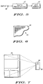
- FIG. 7 a perspective view of portable, or hand-held, electronics equipment 65 is illustrated with miniature image manifestation apparatus mounted therein so that only a viewing aperture 66 is visible.
- FIG. 7 further illustrates a typical view 70 seen by an operator looking into viewing aperture 66 of electronics equipment 65, which view 70 appears to be behind electronics equipment 65.
- View 70 could be, for example, a floor plan of a building about to be entered by the operator (a policeman). The floor plan is on file at the police station and, when assistance is requested by the policeman, the station simply transmits the previously recorded plan.
- electronics equipment 65 might be utilized to transmit pictures of missing persons or wanted criminals, maps, extremely long messages, etc. Many other variations, such as silent receiver operation wherein the message appears in viewing aperture 66 instead of audibly, are possible.
- magnifier 12 can be manufactured very small, with high angular magnification and very inexpensively. Also, while injection molding the various optical elements to incorporate the diffractive optical elements and/or the aspherical surfaces is considered the optimum manufacturing method, it is also the least expensive. Further, because of the small size, high angular magnification and rugged construction of magnifier 12 , magnifier 12 can be used in conjunction with miniature image manifestation apparatus 10 and/or in virtually any portable electronics equipment.
Abstract
Description
- The present invention pertains to optical magnifiers and more specifically to optical magnifiers incorporating a single fold in the optical path.
- With the advent of the communications era, one of the major markets for optical devices is portable electronics equipment, such as cellular telephones, pagers, two-way radios, data banks, computers and the like. Generally, it is desirable that the optical source devices in this type of equipment are compact with low power, inexpensive and include high quality optics with large angular magnification. However, large angular magnification requires a small focal length, as can be seen from the relationship for angular magnifying power (MP) set forth below. Generally, in the discussion below the optical system is treated as a single lens for convenience in describing the relationships.

- V
- is a constant, the distance of distinct vision (approximately 10" or 254mm);
- b
- is the distance from the lens to the virtual image;
- e
- is the distance from the lens to the eye; and
- f
- is the effective focal length.
- A small effective focal length in turn requires that the optical system have a small F/No., which translates into a fast system in the applications being described. Generally, a fast system is defined as a system with an F/No. less than or equal to approximately 2. As is known in the art, the F/No. is determined by the ratio of the focal length to the diameter of the lens.
- Thus, as the focal length is reduced and the system is made smaller, it is inherent that a larger area of the lens, or lens system, is used. This use of a larger area of the lens system results in greater aberration in images transmitted through the system and a need for greater aberration correction. As is well understood by those skilled in the art, greater aberration correction means more elements in the system, which in turn means larger size and greater cost. Therefore, a major problem that is inherent in any attempts to produce compact, inexpensive, high quality optics with large angular magnification is aberration correction.
- Several different attempts have been made to provide optical systems for portable electronic devices, one of which includes all refractive or reflective optics with a single line of pixels and a vibrating mirror. The single line of pixels is sequenced through the rows of a raster and, simultaneously, the vibrating mirror scans the line of pixels to properly position each subsequent row in its proper orientation. The problem with this system is the high accuracy of timing required, the amount of power used and the blurring of the ultimate image by the vibrations of the mirror. Also, this system is extremely fragile and not conveniently adaptable to the rough use normally occurring in portable equipment.
- The system that is normally used at the present time is one using a large image source and either a direct view image or low magnification optics. The major problem with this system is that it greatly limits the size of the portable electronics on which it is used. Basically, the image must be large enough for an operator to read and/or understand the information being displayed. Thus, for example, if one wanted to display an 8.5" by 11" sheet of paper (a standard letter), the direct view display must be 8.5" by 11" to be easily read. Such a display is clearly too large to be incorporated into most portable communications devices, such as pagers, two-way radios, cellular phones and the like.
- It would be highly desirable to devise an optical system with the attributes of being compact and inexpensive, and including high quality optics with large angular magnification, while correcting for aberrations.
- It is a purpose of the present invention to provide a very small, compact and relatively inexpensive optical magnifier.
- It is another purpose of the present invention to provide a very small, compact and relatively inexpensive optical magnifier which includes high quality optics with relatively large angular magnification.
- It is still another purpose of the present invention to provide a very small, compact and relatively inexpensive optical magnifier which includes high quality optics with relatively large angular magnification with aberration correction.
- It is a further purpose of the present invention to provide a, compact and relatively inexpensive optical magnifier which includes high quality optics with relatively large angular magnification with aberration correction, which is small enough to conveniently fit in portable electronic equipment..
- The above problems and others are substantially solved and the above purposes and others are realized in a single fold optical magnifier including a plurality of optical elements having an inlet with a light outlet directed at an angle to the inlet and a reflecting surface positioned to direct light from the inlet to the outlet. The optical elements define a light path from the inlet to the outlet with a total average optical length of approximately 15 to 35 millimeters. The plurality of optical elements includes at least one aspheric surface to correct for aberration and at least one diffractive optical element positioned in the light path to provide additional aberration correction. The optical elements are constructed to angularly magnify images by at least a power of ten.
- The above problems and others are substantially solved and the above purposes and others are further realized in image manifestation apparatus for use in small portable electronics equipment. The image manifestation apparatus includes an image generator with a two dimensional array of light emitting devices formed on a single substrate and driver circuits coupled to the light emitting devices and including a data input terminal. The light emitting devices are individually addressable by the driver circuits so as to generate a real image including one of a plurality of lines of alpha-numerics and graphics from data received at the data input.
- A single fold optical magnifier is positioned with an image inlet adjacent the image generator so as to receive the real image generated by the image generator. The magnifier includes a plurality of optical elements having an inlet defining the image inlet of the single fold optical magnifier and a light outlet directed at an angle to the inlet, with a reflecting surface optically positioned between the inlet and the outlet so as to direct light from the inlet to the outlet. The light outlet defines a viewing aperture and the plurality of optical elements produce a virtual image from the real image, which virtual image is viewable at the viewing aperture.
- The plurality of optical elements define a light path from the light inlet to the light outlet with a total average optical length in the range of approximately 15 to 35 millimeters. The plurality of optical elements include at least one aspheric surface to correct aberrations and at least one diffractive optical element positioned in the light path so as to provide further aberration correction. The optical elements are constructed to angularly magnify the real image generated by the image generator into a virtual image greater than ten times larger than the real image.
- Referring to the drawings:
- FIG. 1 is a view in top plan of image manifestation apparatus employing a single fold optical magnifier in accordance with the present invention;
- FIG. 2 is a front view of the apparatus illustrated in FIG. 1;
- FIG. 3 is a view in side elevation, portions thereof broken away and shown in section, of the apparatus illustrated in FIG. 1;
- FIG. 4 is a 4x magnified view in side elevation of the apparatus illustrated in FIG. 1;
- FIG. 5 is a simplified block diagram of an image generator associated with the apparatus of FIG. 1;
- FIG. 6 is an enlarged view in top plan of an array of light emitting devices, portions thereof broken away, forming a portion of the image generator of FIG. 5; and
- FIG. 7 is a view in perspective illustrating a typical view as seen by the operator of portable communications equipment employing the image manifestation apparatus of FIG. 1.
- FIGS. 1, 2 and 3 illustrate a top plan view, front view, and side elevation of miniature
image manifestation apparatus 10 incorporating a single foldoptical magnifier 12 in accordance with the present invention. FIGS. 1, 2 and 3 illustrate miniatureimage manifestation apparatus 10 approximately the actual size to provide some indication as to the extent of the reduction in size achieved by the present invention.Apparatus 10 includes anarray 15 of light emitting devices, such as organic or inorganic LEDs, field emission devices, vertical cavity surface emitting lasers, LCDs, etc. In this specific embodiment,array 15 includes 144 light emitting devices by 240 light emitting devices. Each light emitting device is fabricated approximately 20 microns on a side with a center-to-center spacing between adjacent devices of no more than 20 microns. Each light emitting device is turned ON with approximately 1.8 volts and utilizes approximately 50µA of current when it is turned ON.Array 15 produces a luminance less than approximately 15 fL. -
Array 15 is mounted on the under-surface of aglass substrate 16 and adriver board 18 is bump-bonded tosubstrate 16. Additional information on driver boards and bonding of substrates to the driver boards is disclosed in a copending United States patent application entitled "Integrated Electro-optical Package", serial number 08/216,995, filed on March 24, 1994 and assigned to the same assignee, which information is included herein by reference. - Single fold
optical magnifier 12 is also mounted onsubstrate 16 and includes a plurality of optical elements defining a light path fromarray 15 to aviewing aperture 19, best seen in FIG. 2. The plurality of optical elements are constructed to angularly magnify images, generated byarray 15, at a light inlet of a first optical element by greater than ten. Because of the length of the optical path and the size of array 15 (the real image), the horizontal field of view of the optics ranges from approximately 11 degrees at a magnification of 10x to 22 degrees at a magnification of 20x, with the present embodiment having a horizontal field of view of approximately 16 degrees and a magnification of 15x. - Referring specifically to FIG. 4, a 4x magnified view in side elevation of portions of
apparatus 10 of FIG. 1 is illustrated for clarity. From this view it can be seen that the plurality of optical elements includes a firstoptical element 20 having alight inlet 22, a spheric surface serving as alight outlet 23 and directed at an angle tolight inlet 22 and a reflectingsurface 25 optically positioned betweenlight inlet 22 andlight outlet 23 so as to direct light fromlight inlet 22 tolight outlet 23. In this specific embodiment,element 20 is formed as a prism and is molded from an optical quality plastic. Generally, it is understood that optical quality plastic is material having a high index of refraction, between approximately 1.5 and 1.6. Reflectingsurface 25 may be a separate silvered mirror that is simply molded intoelement 20, orsurface 25 can be silvered after formation ofelement 20, orsurface 25 can be uncoated and used in a total internal reflection mode. - In this embodiment,
light inlet 22 takes the form of an aspheric field flattening concave surface molded directly intoelement 20 and formed as an integral part thereof. It will be understood, however, thatlight inlet 22 could be formed as a separate lens and subsequently positioned in optical alignment with the lower surface ofelement 20. Separate components of course result in additional components and assembly steps which can increase the cost and size of the final structure. - Reflecting
surface 25 is disposed, with respect tolight inlet 22 andlight outlet 23, to fold or bend light passing throughfirst element 20 at an angle between approximately 80° to 100°. More specifically, in the embodiment illustrated, light is reflected at an angle of approximately 95°. It has been found, for example, that an angle of 95° avoids vignetting on the lower part of the image at the outlet ofoptical magnifier 12. - A significant part of the design of
first element 20 is the use of a solid, single fold prism with a convex outlet face to enable increased angular magnification (reduced effective focal length) in the same volume of space compared to the use of a simple turning mirror in the air. - In many applications it may be desirable to include apparatus for focusing the final image. To this end, element 20 (and the other elements to be described, if desired) is mounted on
substrate 16 by means of a threadedadjustment 27 which can be rotated by a thumb screw, screwdriver, etc., to move the fixed assembly ofelements substrate 16 andarray 15. Focusing is accomplished by simply changing the distance betweenlight inlet 22 and the image generated onarray 15. - The plurality of optical elements further includes an
optical lens 30 having alight inlet 32, positioned adjacentlight outlet 23 of firstoptical element 20, and alight outlet 34. In the specific embodiment illustrated,optical lens 30 is a biaspheric optical lens having an aspheric surface defininglight inlet 32 and an aspheric surface defininglight outlet 34.Optical lens 30 is fixedly mounted relative tofirst element 20 by any convenient means including an outer housing (illustrated schematically in FIGS. 1 - 3), a mounting frame, or any other convenient structure. The aspheric surfaces, includinglight outlet 34,light inlet 32,light outlet 23 and field flatteninglight inlet 22 are designed to reduce and/or eliminate any aberration in wavefront as it passes fromlight inlet 22 tolight outlet 34. - The plurality of optical elements, including
first element 20 andoptical lens 30, define a light path fromlight inlet 22 offirst element 20 tolight outlet 34 ofoptical lens 30. To fabricate a single fold optical magnifier that is useful in portable electronic devices, the total average optical length of the optical path should be in the range of approximately 15 to 35 millimeters. In this embodiment the optical path fromlight inlet 22 to the aspheric surface defininglight outlet 34 is approximately 20 millimeters. - Also, the plurality of optical elements, including
first element 20 andoptical lens 30, are constructed to include at least one diffractive optical element positioned in the light path so as to provide additional, primarily chromatic (in this embodiment), aberration correction. In the embodiment illustrated, a diffractiveoptical element 35 is incorporated into the aspheric surface defininglight inlet 32. It will of course be understood that diffractive optical elements can, instead or in addition to, be included in any other surface of the plurality of elements inoptical magnifier 12. If a diffractive optical element is included in a surface that is substantially normal to the light path, as opposed to those in which the light strikes the surface at an angle, the diffractive optical element is somewhat easier to construct because of rotational symmetry, whereas surfaces on which light strikes at an angle have nonrotational symmetry. Because the aspheric surfaces and diffractiveoptical element 35make lens 30 relatively complex, it has been found that fabrication ofoptical lens 30 is best done by injection molding. - While
first element 20 andlens 30 can be constructed to form a complete magnifier, in this specific embodiment, a low poweroptical lens 40 is included as an example of possible extensions of the magnifier.Optical lens 40 includes aspheric surface 41 which defines a light input and aspheric surface 42 which defines a light output. Also,surface 41 has a diffractiveoptical element 45 formed in thesurface 41 to provide additional aberration correction.Optical lens 40 is mounted adjacentoptical lens 30 and forms an outlet optical element that defines an aperture through which the angularly magnified image can be viewed. The addition ofoptical lens 40 may add somewhat to the size and complexity ofmagnifier 12, but provides some angular magnification and aberration correction that reduces the complexity of the various other elements, which can in many applications reduce the overall cost ofmagnifier 12. Because of its low power,lens 40 may also be used as the package window, or viewing aperture. In applications in which onlyfirst element 20 andoptical lens 30 are utilized, it may be convenient to define the viewing aperture with a glass or plastic window, which may be clear, a light filter, etc. - A typical design specification, or prescription, for the three element magnifier of FIG. 1 is listed below for example only.

- Here it should be noted that because of the very
small magnifier 12 andarray 15 and the fact that a virtual image is utilized, rather than a direct view display, the overall physical dimensions of miniatureimage manifestation apparatus 10 are approximately 1.5 inches (3.8 cm) wide by 0.75 inches (1.8 cm) high by 1.75 inches (4.6 cm) deep, or a total volume of approximately 2 cubic inches (32 cm3), of which less than 0.7 cubic inches is the optic volume. -
Array 15 is illustrated in more detail in FIG. 5 and includes, for example, semiconductor electronics such as a light emitting device (LED)array 55 driven bydata processing circuits 57. The LEDs may be, for example, organic or inorganic light emitting diodes, vertical cavity surface emitting lasers, field emission devices, etc.Data processing circuits 57 include, for example, logic and switching circuit arrays for controlling each LED inLED array 35, drivers and the like.Data processing circuits 57 include, in addition to or instead of the logic and switching arrays, a microprocessor or similar circuitry for receiving data at aninput terminal 58 and processing the data to produce a desired real image on a device such asLED array 55. - In this specific
embodiment LED array 55 is utilized because of the extremely small size that can be achieved and because of the simplicity of construction and operation. Referring specifically to FIG. 6, a plan view ofLED array 55 is illustrated in which pixels are formed in a regular pattern of rows and columns on a single substrate (e.g. a semiconductor chip) 60. Each pixel includes at least one LED, with additional parallel LEDs being included, if desired, for color, additional brightness and/or redundancy. By addressing specific pixels by row and column in a well known manner, the specific pixels are energized to produce a real image. Digital or analog data is received atinput terminal 58 and converted bydata processing circuits 57 into signals capable of energizing selected pixels to generate the predetermined real image. The digital or analog data is received from any data source, such as a communication receiver, a memory or data bank, or other portable electronic device, etc. - It will be understood by those skilled in the art that LED
array 55 andsubstrate 60 are greatly enlarged in FIG. 6. Also, whiledata processing circuits 57 are represented by a separate block, it will be understood that in some applications they may be formed around the edge ofarray 55 onsubstrate 60. The actual size ofsubstrate 60 is on the order of a few milli-meters (e.g. 3 to 10) along each side with each LED being on the order of 5 to 50 microns on a side (or in diameter if the LED is round). Because of the extremely small size ofsubstrate 60, drive lines or metal connecting traces between LEDs, have a very small cross-section, which severely limits their current carrying capacity, or current density. Referring to FIG. 6 for example, in one typical operation only a row at a time is addressed or "turned ON". Thus, the metal trace for each column needs to carry only sufficient current for one LED (the one LED in the row which is ON). However, all of the LEDs in the ON row could potentially be turned ON simultaneously. Thus, the metal trace for the ON row, which can potentially be required to carry current for however many LEDs are in the row (e.g. 100 to 1500 LEDs), must carry many times as much current as the column metal traces. - Referring again to FIG. 4, the operation of miniature
image manifestation apparatus 10 will be described generally.Array 15 ofapparatus 10 provides a real image source at the lower surface ofsubstrate 16. The aspheric field flattening concave surface defininglight inlet 22 is positioned in spaced relation tosubstrate 16 and generally flattens the image, to correct some aberration problems, and spreads the light across the surface of reflectingsurface 25.Surface 25 reflects the light throughlight outlet 23 and ontolight inlet 32 ofoptical lens 30. As the light passes through the spheric surface defininglight outlet 23, less aberration is introduced than in a plano surface. Diffractiveoptical element 35 is specifically designed to correct additional, primarily chromatic, aberration and the aspherical surface defininglight inlet 32 corrects and/or balances more aberration.Optical lens 30 provides the primary angular magnification and the aspherical surface defininglight outlet 34 corrects and/or balances more aberration. - If
optical lens 40 is included in the apparatus, diffractiveoptical element 45 and/or anaspherical surface 41 can be included to correct for additional aberration.Optical lens 40 also provides a small amount of additional angular magnification.Surface 42, defining the viewing aperture of the apparatus, can be an aspherical surface to further correct aberration if desired. Depending upon the application, magnification and optical path length, the optical elements for the magnifier generally include at least one aspherical surface and at least one diffractive optical element in the light path. In some special applications it may be possible to use all aspherical surfaces and no diffractive optical elements and in some very special applications it may be possible to use only diffractive optical elements to correct aberration. It should be noted, in any case, that the present invention allows aberration correction to be enhanced through the use of aspheric and diffractive structures, sometimes on the same surface, thus avoiding additional conventional elements. It should also be noted that in order to economically form the aspheric and/or diffractive optical elements on the small surfaces of the optical elements that it is generally necessary to mold the optical elements. - Referring to FIG. 7, a perspective view of portable, or hand-held,
electronics equipment 65 is illustrated with miniature image manifestation apparatus mounted therein so that only aviewing aperture 66 is visible. FIG. 7 further illustrates atypical view 70 seen by an operator looking intoviewing aperture 66 ofelectronics equipment 65, which view 70 appears to be behindelectronics equipment 65.View 70 could be, for example, a floor plan of a building about to be entered by the operator (a policeman). The floor plan is on file at the police station and, when assistance is requested by the policeman, the station simply transmits the previously recorded plan. Similarly,electronics equipment 65 might be utilized to transmit pictures of missing persons or wanted criminals, maps, extremely long messages, etc. Many other variations, such as silent receiver operation wherein the message appears inviewing aperture 66 instead of audibly, are possible. - Thus, an optical system with the attributes of being compact and inexpensive, and including high quality optics with large angular magnification, while correcting for aberrations, has been disclosed. Because of its novel construction,
magnifier 12 can be manufactured very small, with high angular magnification and very inexpensively. Also, while injection molding the various optical elements to incorporate the diffractive optical elements and/or the aspherical surfaces is considered the optimum manufacturing method, it is also the least expensive. Further, because of the small size, high angular magnification and rugged construction ofmagnifier 12 ,magnifier 12 can be used in conjunction with miniatureimage manifestation apparatus 10 and/or in virtually any portable electronics equipment. - While we have shown and described specific embodiments of the present invention, further modifications and improvements will occur to those skilled in the art. We desire it to be understood, therefore, that this invention is not limited to the particular forms shown and we intend in the appended claims to cover all modifications that do not depart from the spirit and scope of this invention.
Claims (10)
- A single fold optical magnifier characterized by:
a plurality of optical elements (22, 20, 30, 40) having a light inlet (22) and a light outlet (42) directed at an angle to the inlet (22), with a reflecting surface (25) optically positioned between the inlet (22) and the outlet (42) so as to direct light from the inlet (22) to the outlet (42), the optical elements (22, 20, 30, 40) include at least one aspheric surface (23, 34, 42) for aberration correction;
the plurality of optical elements (22, 20, 30, 40) defining a light path from the light inlet (22) to the light outlet (42) with a total average optical length in the range of approximately 20 to 35 millimeters; and
at least one diffractive optical element (35) positioned in the light path so as to provide further aberration correction; and
the plurality of optical elements (22, 20, 30, 40) being constructed to angularly magnify an image source (15) at the light inlet (22) of the first optical element by greater than ten. - A single fold optical magnifier as claimed in claim 1 further characterized in that the light outlet (42) is directed at an angle to the inlet (22) in a range of approximately 80° to 100°.
- A single fold optical magnifier as claimed in claim 2 further characterized in that the light outlet (42) is directed at an angle of approximately 95° to the inlet (22).
- A single fold optical magnifier as claimed in claim 1 further characterized in that the total average optical length of the light path is approximately 20 millimeters.
- A single fold optical magnifier as claimed in claim 1 further characterized in that the plurality of optical elements (22, 20, 30, 40) define a horizontal field of view greater than approximately 11 degrees.
- A single fold optical magnifier as claimed in claim 1 further characterized in that the plurality of optical elements (22, 20, 30, 40) is constructed to angularly magnify an image source (15) at the light inlet (22) of the plurality of optical elements (22, 20, 30, 40) by approximately fifteen.
- A single fold optical magnifier as claimed in claim 6 further characterized in that the plurality of optical elements (22, 20, 30, 40) define a horizontal field of view approximately 16 degrees.
- A single fold optical magnifier as claimed in claim 1 further characterized in that the plurality of optical elements (22, 20, 30, 40) includes a first optical element (20) having an aspheric field flattening light inlet (22).
- A single fold optical magnifier as claimed in claim 8 further characterized in that the plurality of optical elements (22, 20, 30, 40) includes a first optical element (20) having an aspheric light outlet (23) directed at an angle to the inlet (22) and a reflecting surface (25) optically positioned between the inlet (22) and the outlet (23) so as to direct light from the inlet (22) to the outlet (23).
- A single fold optical magnifier as claimed in claim 9 further characterized in that the first optical element (20) is a prism with the aspheric field flattening light inlet (22) formed in one side thereof and a reflecting surface (25) formed on a second side thereof.
Applications Claiming Priority (2)
| Application Number | Priority Date | Filing Date | Title |
|---|---|---|---|
| US405057 | 1995-03-16 | ||
| US08/405,057 US5644430A (en) | 1995-03-16 | 1995-03-16 | Single fold optical magnifier for use in image manifestation apparatus |
Publications (2)
| Publication Number | Publication Date |
|---|---|
| EP0732606A2 true EP0732606A2 (en) | 1996-09-18 |
| EP0732606A3 EP0732606A3 (en) | 1996-11-13 |
Family
ID=23602110
Family Applications (1)
| Application Number | Title | Priority Date | Filing Date |
|---|---|---|---|
| EP96103293A Withdrawn EP0732606A3 (en) | 1995-03-16 | 1996-03-04 | A single fold optical magnifier for use in image manifestation apparatus |
Country Status (5)
| Country | Link |
|---|---|
| US (1) | US5644430A (en) |
| EP (1) | EP0732606A3 (en) |
| JP (1) | JPH08262344A (en) |
| KR (1) | KR100405121B1 (en) |
| TW (1) | TW298625B (en) |
Families Citing this family (8)
| Publication number | Priority date | Publication date | Assignee | Title |
|---|---|---|---|---|
| US5708280A (en) * | 1996-06-21 | 1998-01-13 | Motorola | Integrated electro-optical package and method of fabrication |
| US5818634A (en) * | 1996-08-05 | 1998-10-06 | Motorola, Inc. | Dual mode optical Magnifier system |
| US6677936B2 (en) | 1996-10-31 | 2004-01-13 | Kopin Corporation | Color display system for a camera |
| US6545654B2 (en) | 1996-10-31 | 2003-04-08 | Kopin Corporation | Microdisplay for portable communication systems |
| US6486862B1 (en) | 1996-10-31 | 2002-11-26 | Kopin Corporation | Card reader display system |
| JP2005084284A (en) * | 2003-09-08 | 2005-03-31 | Sony Corp | Viewfinder and imaging apparatus |
| DE202018103176U1 (en) | 2018-06-06 | 2018-07-04 | E-Lead Electronic Co., Ltd. | Display device for an enlarged display |
| TWM622202U (en) | 2021-09-08 | 2022-01-11 | 怡利電子工業股份有限公司 | Head mounted fixing device |
Citations (5)
| Publication number | Priority date | Publication date | Assignee | Title |
|---|---|---|---|---|
| US3663092A (en) * | 1969-07-25 | 1972-05-16 | Rodenstock Optik G | Elbow magnifying lens |
| EP0535402A1 (en) * | 1991-09-30 | 1993-04-07 | Motorola, Inc. | Waveguide virtual image display |
| EP0566001A2 (en) * | 1992-04-07 | 1993-10-20 | Hughes Aircraft Company | Wide spectral bandwidth virtual image display optical system |
| EP0617549A1 (en) * | 1993-03-26 | 1994-09-28 | Canon Kabushiki Kaisha | Multi-eye image displaying apparatus |
| US5467215A (en) * | 1994-12-21 | 1995-11-14 | Motorola | Integrated electro-optic package for reflective spatial light modulators |
Family Cites Families (13)
| Publication number | Priority date | Publication date | Assignee | Title |
|---|---|---|---|---|
| US2750677A (en) * | 1951-12-20 | 1956-06-19 | Wirth Armin | Bubble level |
| US3575485A (en) * | 1969-01-02 | 1971-04-20 | Us Navy | Holographic magnifier |
| US3860329A (en) * | 1972-01-03 | 1975-01-14 | Polaroid Corp | Unique prismatic element and mounting arrangement therefor |
| US4099851A (en) * | 1976-05-07 | 1978-07-11 | Gerard Rethore | Reading aid |
| US5035474A (en) * | 1984-04-16 | 1991-07-30 | Hughes Aircraft Company | Biocular holographic helmet mounted display |
| US4869575A (en) * | 1986-05-12 | 1989-09-26 | Iota Instrumentation Company | Headwear-mounted periscopic display device |
| DE3681178D1 (en) * | 1986-12-30 | 1991-10-02 | Ibm Deutschland | SWIVELING ACCESS ARM FOR OPTICAL PANELS. |
| FR2642530A1 (en) * | 1989-01-30 | 1990-08-03 | Seiko Epson Corp | Focusing mechanism and optical head |
| US5075799A (en) * | 1989-07-14 | 1991-12-24 | Motorola, Inc. | Magnifying lens attachment for information display selective call receiver |
| US5148322A (en) * | 1989-11-09 | 1992-09-15 | Omron Tateisi Electronics Co. | Micro aspherical lens and fabricating method therefor and optical device |
| US5044706A (en) * | 1990-02-06 | 1991-09-03 | Hughes Aircraft Company | Optical element employing aspherical and binary grating optical surfaces |
| US5323477A (en) * | 1992-08-24 | 1994-06-21 | Motorola, Inc. | Contact array imager with integral waveguide and electronics |
| US5483362A (en) * | 1994-05-17 | 1996-01-09 | Environmental Research Institute Of Michigan | Compact holographic sight |
-
1995
- 1995-03-16 US US08/405,057 patent/US5644430A/en not_active Expired - Fee Related
-
1996
- 1996-02-27 TW TW085102234A patent/TW298625B/zh active
- 1996-03-04 EP EP96103293A patent/EP0732606A3/en not_active Withdrawn
- 1996-03-13 JP JP8084655A patent/JPH08262344A/en active Pending
- 1996-03-19 KR KR1019960007338A patent/KR100405121B1/en not_active IP Right Cessation
Patent Citations (5)
| Publication number | Priority date | Publication date | Assignee | Title |
|---|---|---|---|---|
| US3663092A (en) * | 1969-07-25 | 1972-05-16 | Rodenstock Optik G | Elbow magnifying lens |
| EP0535402A1 (en) * | 1991-09-30 | 1993-04-07 | Motorola, Inc. | Waveguide virtual image display |
| EP0566001A2 (en) * | 1992-04-07 | 1993-10-20 | Hughes Aircraft Company | Wide spectral bandwidth virtual image display optical system |
| EP0617549A1 (en) * | 1993-03-26 | 1994-09-28 | Canon Kabushiki Kaisha | Multi-eye image displaying apparatus |
| US5467215A (en) * | 1994-12-21 | 1995-11-14 | Motorola | Integrated electro-optic package for reflective spatial light modulators |
Also Published As
| Publication number | Publication date |
|---|---|
| KR100405121B1 (en) | 2004-01-28 |
| KR970066631A (en) | 1997-10-13 |
| US5644430A (en) | 1997-07-01 |
| TW298625B (en) | 1997-02-21 |
| EP0732606A3 (en) | 1996-11-13 |
| JPH08262344A (en) | 1996-10-11 |
Similar Documents
| Publication | Publication Date | Title |
|---|---|---|
| US5699186A (en) | Multi-fold optical magnifier for use in image manifestation apparatus | |
| US6366267B1 (en) | Electronic device with miniature virtual image display | |
| EP0802501B1 (en) | Smart card reader with visual image display | |
| EP0535402B1 (en) | Waveguide virtual image display | |
| US5323477A (en) | Contact array imager with integral waveguide and electronics | |
| EP0831420A2 (en) | Smart card with visual image display | |
| EP0770896B1 (en) | Dual image manifestation apparatus with integrated electro-optical package | |
| US5831699A (en) | Display with inactive portions and active portions, and having drivers in the inactive portions | |
| EP0831352A1 (en) | Optical modulating device, display and electronic device | |
| US5491491A (en) | Portable electronic equipment with binocular virtual display | |
| KR19980018848A (en) | Smart card device with pager and visual image display | |
| EP0817393A2 (en) | Portable power source with visual image display | |
| CN110573932A (en) | Optical system for electronic device with display | |
| EP0732606A2 (en) | A single fold optical magnifier for use in image manifestation apparatus | |
| US5099361A (en) | Projection lens and projection television system using the same | |
| EP0763763A1 (en) | Magnifying image display with multi-mode screen | |
| US5630001A (en) | Image generator for use in image manifestation apparatus | |
| JPH05210066A (en) | Small false image display | |
| EP0807847A2 (en) | Nematic liquid crystal phase spatial light modulator for enhanced display resolution | |
| CN111596512B (en) | Projection lens and projection equipment | |
| WO2001088597A9 (en) | Virtual imaging system for small font text | |
| EP0797116A1 (en) | Stackable optical elements | |
| JP3451387B2 (en) | Aerial display device | |
| CN1164036A (en) | Single fold optical magnifier for use in image manifestation apparatus |
Legal Events
| Date | Code | Title | Description |
|---|---|---|---|
| PUAI | Public reference made under article 153(3) epc to a published international application that has entered the european phase |
Free format text: ORIGINAL CODE: 0009012 |
|
| AK | Designated contracting states |
Kind code of ref document: A2 Designated state(s): DE FR GB |
|
| PUAL | Search report despatched |
Free format text: ORIGINAL CODE: 0009013 |
|
| AK | Designated contracting states |
Kind code of ref document: A3 Designated state(s): DE FR GB |
|
| 17P | Request for examination filed |
Effective date: 19970513 |
|
| 17Q | First examination report despatched |
Effective date: 20011023 |
|
| STAA | Information on the status of an ep patent application or granted ep patent |
Free format text: STATUS: THE APPLICATION IS DEEMED TO BE WITHDRAWN |
|
| 18D | Application deemed to be withdrawn |
Effective date: 20030304 |