EP0726532A2 - Array processor communication architecture with broadcast instuctions - Google Patents
Array processor communication architecture with broadcast instuctions Download PDFInfo
- Publication number
- EP0726532A2 EP0726532A2 EP96480018A EP96480018A EP0726532A2 EP 0726532 A2 EP0726532 A2 EP 0726532A2 EP 96480018 A EP96480018 A EP 96480018A EP 96480018 A EP96480018 A EP 96480018A EP 0726532 A2 EP0726532 A2 EP 0726532A2
- Authority
- EP
- European Patent Office
- Prior art keywords
- instruction
- register
- operand
- designation
- execution unit
- Prior art date
- Legal status (The legal status is an assumption and is not a legal conclusion. Google has not performed a legal analysis and makes no representation as to the accuracy of the status listed.)
- Granted
Links
Images


Classifications
-
- G—PHYSICS
- G06—COMPUTING; CALCULATING OR COUNTING
- G06F—ELECTRIC DIGITAL DATA PROCESSING
- G06F15/00—Digital computers in general; Data processing equipment in general
- G06F15/16—Combinations of two or more digital computers each having at least an arithmetic unit, a program unit and a register, e.g. for a simultaneous processing of several programs
- G06F15/163—Interprocessor communication
- G06F15/173—Interprocessor communication using an interconnection network, e.g. matrix, shuffle, pyramid, star, snowflake
- G06F15/17356—Indirect interconnection networks
- G06F15/17368—Indirect interconnection networks non hierarchical topologies
- G06F15/17381—Two dimensional, e.g. mesh, torus
Definitions
- the invention disclosed broadly relates to data processing systems and method and more particularly relates to improvements in array processor architectures.
- a plurality of processor elements are connected in a cluster by a common instruction bus to an instruction memory.
- Each PE has data buses connected to at least its four nearest PE neighbors, referred to as its North, South, East and West PE neighbors.
- Each PE also has a general purpose register file containing several operand registers.
- a common instruction is broadcast from the instruction memory over the instruction bus to each PE in the cluster.
- the instruction includes an opcode value that controls the arithmetic or logical operation performed by an execution unit in the PE on an operand from one of the operand registers in the register file.
- a switch is included in each PE to interconnect it with a first PE neighbor as the destination to which the result from the execution unit is sent.
- the broadcast instruction includes a destination field that controls the switch in the PE, to dynamically select the destination neighbor PE to which the result is sent. Further in accordance with the invention, the broadcast instruction includes a target field that controls the switch in the PE, to dynamically select the operand register in the register file of the PE, to which another result received from another neighbor PE in the cluster is stored. In this manner, the instruction broadcast to all the PEs in the cluster, dynamically controls the communication of operands and results between the PEs in the cluster, in a single instruction, multiple data processor array.
- Fig. 1 is a high level array machine organization diagram for multiple control units.
- Fig. 2 is an example instruction format for communications, in accordance with the invention.
- Fig. 3 is a second example instruction format for communications, in accordance with the invention.
- Fig. 4 is a single processor element (diagonal) node flow with connection interfaces.
- Fig. 5 is a dual processor element node flow with connection interfaces.
- Fig. 6 is a nearest-neighbor communication example in a single processor element node.
- Fig. 7 is a nearest-neighbor communication example in a dual processor element node.
- Fig. 8 is a logical and folded mesh representation of adjacent processor element column communications.
- Fig. 9 is a logical and folded mesh representation of adjacent processor element row communications.
- Fig. 10 is a flow organization of a processing element, depicting the flow of an individual processing element, showing all its arithmetic facilities and the points to find for connection to switch logic and paired processor elements.
- Fig. 11 is a general form diagram of the data select unit.
- Fig. 12 is an example of a data select unit in use, wherein byte B of the source is placed in the low order 8 bits of the destination register and all the remaining destination bits are forced to be the same as the sign of the byte, as performed by the data selector logic.
- Fig. 13 is a flow chart showing folded array fast odd/even symmetric 1-D DCT.
- Fig. 14 illustrates the execution of a butterfly surrogate.
- Fig. 15 illustrates the first execution of multiply add and DSU send surrogate.
- Fig. 16 illustrates the second execution of multiply add and DSU send surrogate.
- Fig. 17 illustrates the third execution of multiply add and DSU send surrogate.
- Fig. 18 illustrate the fourth execution of multiply add and DSU send surrogate.
- Fig. 19 illustrates the execution of the butterfly with a clustered processor element destination surrogate.
- Fig. 1 depicts a high level view of the Mwave array processor machine organization.
- the machine organization is partitioned into three main parts: the System Interfaces including Global Memory 100 and external I/O, multiple Control Units 103 with Local Memory 102, and the Execution Array with Distributed Control PEs 104.
- the System Interface is an application-dependent interface through which the Mwave array processor interfaces with Global Memory, the I/O, other system processors, and the personal computer/workstation host. Consequently, the System Interface will vary depending upon the application and the overall system design.
- the Control Units 103 contain the local memory 102 for instruction and data storage, instruction fetch (I-Fetch) mechanisms, and operand or data fetch mechanisms (D-Fetch).
- the Execution Array with Distributed Control PEs 104 is a computational topology of processing elements chosen for a particular application.
- the array may consists of N Processing Elements (PEs) 104 per control unit 103, with each PE containing an Instruction Buffer (IMRY) 106, a General Purpose Register File (GPRF) 108, Functional Execution units (FNS) 110, Communication Facilities (COM) 112, and interfaces to its Instruction bus 114 and its data buses.
- the PEs may also contain PE-local instruction and data memories. Further, each PE contains an instruction decode register 116 shown in Figure 4, which supports distributed control of the multiple PEs. Synchronism of local memory accessing is a cooperative process between the control units 103, local memories 102, and the PEs 104.
- the array of PEs allows computation functions (FNS) to be executed in parallel in the PEs and results to be communicated (COM) between PEs.
- multiple single instruction, multiple data (MSIMID) machine organization e.g. Fig. 1
- MSIMID multiple single instruction, multiple data
- Fig. 1 it is possible to create single or multiple thread machines wherein the topology of PEs and communication facilities can be configured for a more optimum topology depending upon the application.
- some possible machine organizations are; multiple linear rings, a nearest neighbor 2-dimension mesh array, a folded nearest neighbor 2-dimension mesh, multiple-fold mesh, a 2-dimension hexagonal array, a folded 2-dimension hexagonal array, a folded mesh of trees, combinations of the above as well as others.
- the basic concept involved in the Mwave array processor family is that the communications of results between direct-attached processing elements can be specified in the processing element instruction set architecture 115.
- the destination of results from functional execution units is implied to be the processor's own register file breaks this "tradition", changing the definition of result destination, an implied single processor local destination, a directly-connected multiple processor destination.
- This architecture and directly-connected PE-to-PE links we can claim that communications between the directly connected PEs can be done with zero communication latency.
- the architecture provides this capability by including a destinatio field 120 in the simplex instructions 115 indicating the directly-connected succeeding PE where the result target register resides, which is specified by the target field 126.
- Figure 2 shows a basic simplex 32-bit instruction 115 used in the processor, though 16-bit, 64-bit, etc. formats can use the same principle.
- a North, East, West, and South PE destination is coded in the Destination Extension field 120 is providing a 4-bit field here to allow for growth up to eight clustered processors (used in a three fold array) and up to an eight neighborhood array.
- Examples of topologies with direct-attached PEs are a nearest neighbor mesh, a folded mesh, a tree array, hypercubes, etc. It should also be appreciated that due to the clustering and nearest neighbor mesh organizations, the Physical Design process will physically place the directly connected PEs in close proximity to each other supporting short cycle times.
- this binding of the communications destination specification in the instruction set format is done purposely to, not only provide 0-communication latency, but also to ensure hazard free communications in a SIMD array of processing elements.
- the processor is used to describe the architectural details involved in implementing the described communications concept.
- the Operand-1 field 122, Operand-2 field 124, and Target field 126 are register specifications and the Destination field 120 specifies the direct attached succeeding processing element to which the result is to be communicated.
- the opcode field 128 specifies the arithmetic or logical operation to be performed by a selected execution unit.
- the single, diagonally folded array processor Element (PE) data flow will be briefly described.
- the folded-array nodes are of two types: diagonal nodes containing a single Processing Element, and all other nodes which contain two PEs each. The details of each type are discussed in the following sections.
- each folded array node has the Processing Element (PE) 104.
- PE Processing Element
- the folded array has two node types: those containing a single Processing Element and those containing dual Processing Elements.
- the single-PE nodes are those on the diagonal of the folded mesh; there are four such nodes in the array. The remaining six nodes contain 2 PEs each. Overall, then, there are 16 Processing Elements in the folded 4x4 array distributed among ten nodes.
- All Processing Elements 104 in Figure 4 contain a common set of arithmetic flow components, including a fixed point/floating point Multiply/Add Unit (MAU) 110, an ALU 110a, a Data Select Unit (DSU) 110b, and a General Purpose Register File (GPRF) 108 comprising 32 GPRs.
- Each PE 104 also contains instruction pipeline hardware.
- PE Decode Register (PDR) 106, instruction decode logic, and PE Execute Register (PXR) to hold instructions being executed by the PE.
- PXR PE Execute Register
- SIM Surrogate Instruction Memory
- Logic around the SIM allows for loading the SIM using instructions specifically designed for that purpose.
- a local-PE data memory is included for each PE along with associated load and store address generation units.
- This common set of flow components is augmented with different switch elements and other logic to create the single-PE node and dual-PE nodes that comprise the folded array.
- each PE implements its own instruction pipeline logic, including instruction decode and execute registers (their abbreviated names are PDR and PXR) and instruction decode logic.
- PDR and PXR instruction decode and execute registers
- One thing a PE can't do is to determine its own instruction thread (it has no Instruction Address Register and associated sequencing logic).
- the Sequence Processors (SPs) or control unit 103 serve to accomplish the instruction fetch tasks for both themselves and their associated PEs 104.
- the PEs connected to a given SP 103 are then fed instructions 115 by the SPs 103.
- the instructions 115 are broadcast over the instruction bus 114 to all connected PEs.
- Each PE 104 registers these instructions (in the PDR) and subsequently decodes and executes them.
- SIM Surrogate Instruction Memory
- SIM which may be a combination of RAM and ROM
- compound instructions instructions which cause execute actions in multiple flow elements. Instructions of this type tend to be more complicated than ordinary instructions, and generally will require more bits to represent than are available in a single PE instruction word.
- a technique is proposed whereby a compound (long) instruction is represented in an instruction stream by a surrogate, or place holder instruction. Then, when the surrogate is seen in the instruction stream (by logic in the PE), a compound instruction specified by the surrogate is accessed from SIM and executed in place of the surrogate. Other logic in the PE facilitates loading compound instructions into SIM using specialized instructions. Of course, if some compound instructions are held in ROM, it is never necessary to load them. Some combination of ROM- and RAM-based SIM is probably desirable for most applications.
- Fig. 4 shows the flow for a single-PE (diagonal) processing node.
- the node contains the full complement of components provided by a single PE 104 (MAU, ALU, DSU, GPRF, and local-PE data memory), plus switch/select logic to direct nearest-neighbor and D-bus data to and from the registers.
- the instruction pipeline path logic which is provided allows for orderly decoding and execution of ordinary instructions and surrogate instructions.
- the dual-PE node flow proposed for the folded-mesh array contains all the arithmetic elements of two PEs 104 and 104'. That is, it has 2 MAUs, 2 ALUs, 2 DSUs, 2 sets of GPRs, and 2 local-PE data memories. Switching logic 112 common to the 2 PEs allows for 4 nearest-neighbor communication paths and 2 data bus connections.
- the node halves they are referred to simply as the Top and Bottom PEs) execute separate instructions, so each has its own instruction registers and decode logic.
- multiplexors on the GPRF input ports allow load data from any source to be written into either GPRF via a transpose destination specification.
- the first mode control register contains configuration bits, I-Bus Switch, D-Bus Switch, Nearest-Neighbor/Adjacent-PE Communications Mode, and Ring/Array Mode.
- the second mode control register contains arithmetic options for Rounding and Saturation control of specific execution unit results.
- Two PE instructions control the loading of the two registers.
- the PE Set Mode Instruction controls the configuration bits and loads all PEs with immediate mode control information contained in the instruction.
- the PE Set Rounding/Saturation Instruction loads the second register.
- the I-Bus and D-Bus switches are controlled from this mode register which specifies in the dual PEs how the two IA/IB bus ports and the two DA/DB bus ports are connected to the top and bottom PE. Using these switch settings the I-buses and D-buses can be connected to the row PEs or the column PEs. Additional mode bits indicate whether the PEs are in a Nearest Neighbor or Adjacent-PE Communications mode. Mode information must also be provided for how the PE-to-PE interface is to be used when independent row rings or column rings are used, since the nearest neighbor/Adjacent-PE interface is modified accordingly. The following lists the operational mode bit definitions.
- the PE flow diagrams depicted in Fig. 4 and Fig. 5 show switches which are controlled from instructions being executed. Three types of switches are indicated in the nodes: the PE-NET Switch, Data-Bus (D-Bus) Switch, and Instruction-Bus (I-Bus) switch (only in the dual-PE node).
- the PE-NET switches are controlled by instructions executing in the PEs; the I-Bus and D-Bus switches are controlled by the PE-mode control register.
- the PEs exchange data in different ways among nodes by controlling the PE-NET switches.
- the Nearest-Neighbor (PE-NET) transmitting/receiving facilities for dual-PE nodes include four bi-directional or four input and four output driver/receiver ports.
- For the separate input/output port case there is an input and output pair assigned to each nearest neighbor direction.
- another port will also be directed to simultaneously receive data from a different PE.
- Controls are provided to assure that only two of the driver/receiver ports are simultaneously transmitting data and two others are simultaneously receiving data.
- the diagonal PEs (Fig. 4) share the West/North ports and the South/East ports and thus require only two nearest-neighbor type I/O ports per diagonal PE. Note that in the dual-PE nodes, the receiving/transmitting mechanisms consist of four I/O ports.
- Fig. 6 and Fig. 7 depict the single-PE and dual-PE nodes in a less detailed form than Fig. 4 and Fig. 5 and show examples of how the nearest-neighbor ports are used in supporting four possible transmission modes.
- the communication modes supported cause data to be transmitted in the four cardinal directions and simultaneously received from the opposite direction. For example, transmit North and receive from the South.
- Fig. 8 and Fig. 9 depict, for a four neighborhood array, the logical representation (i.e. on the unfolded mesh) and the folded mesh representation of the four communications modes possible:
- the folded-array nodes each contain one or two Processing Elements as shown in Fig. 4 and Fig. 5.
- the PEs which are all identical, each contain two general types of arithmetic units &dash. an ALU and a fixed point/floating point Multiply/Add Unit (MAU) &dash. a Data Selection Unit (DSU), a Local Load Data Address Generator, a Local Store Data Address Generator, and a set of 32 GPRs which serves to hold operands and working results for operations performed in the node.
- the register set is referred to as the General Purpose Register File, or GPRF for short.
- a view of the PE data flow organization, showing its individual processing elements and GPR file, is shown in Fig. 10.
- Multiply/Add Unit MAU instructions Three classes of Multiply/Add Unit MAU instructions are architectured, one for 16x16 single 32-bit fixed point results, a second for 32x32/dual-16x16 double 32-bit fixed point results, and a third for Single Precision Real Single Precision Real floating point multiply-add results.
- An array processor can be designed to support any one of these options and operate as subsets of the full architecture. With a 64-bit result (or double 32-bit results) the low 32-bit half uses bus Q. For an implementation with a 16x16 MAU only, the Q bus is not used. For a 32-bit Mfast processor the 32x32 MAU instructions are only able to write their results back to a local GPRF.
- the DEST destination field is not used in 32x32 MAU instructions and the second 32-bit result is written back to the target register specified plus one.
- Use of the clustered communications and nearest neighbor interface for the 32x32 MAU instructions is reserved for future machines with 64-bit Nearest Neighbor ports.
- the Processing Element flow does not include any of the switch logic required for communication among array nodes; that logic is unique to the nodes themselves.
- the idea, here, is that the logic for the PE can be designed as a macro and used repeatedly to build the array. It is intended for the PE to be designed with 6 unconnected GPRF input ports, and allow these inputs to be connected in the manner appropriate for the particular node in which the PE is included.
- Fig. 10 indicates typical direct connections (shown in dashed lines) from the ALU, MAU, and DSU. A more complete picture of these direct connections is shown in the Single-PE node flow diagram (Fig. 4).
- the GPRF input ports may also be multiplexed as shown in the Dual-PE node flow diagram (Fig. 5 ).
- the Data Select Unit is used in register-to-register moves and data shift operations.
- a SWAP function can be achieved.
- the general form of the DSU is shown in Fig. 11 :
- the logic in the Data Selector is used to modify the data passing from source to destination for those instructions which require it. For example, when a byte is selected from the source register and then loaded into the destination in sign-extended form, the Data Selector will perform the byte-alignment and sign-extension functions. A simple example of this kind of operation is shown in Fig. 12.
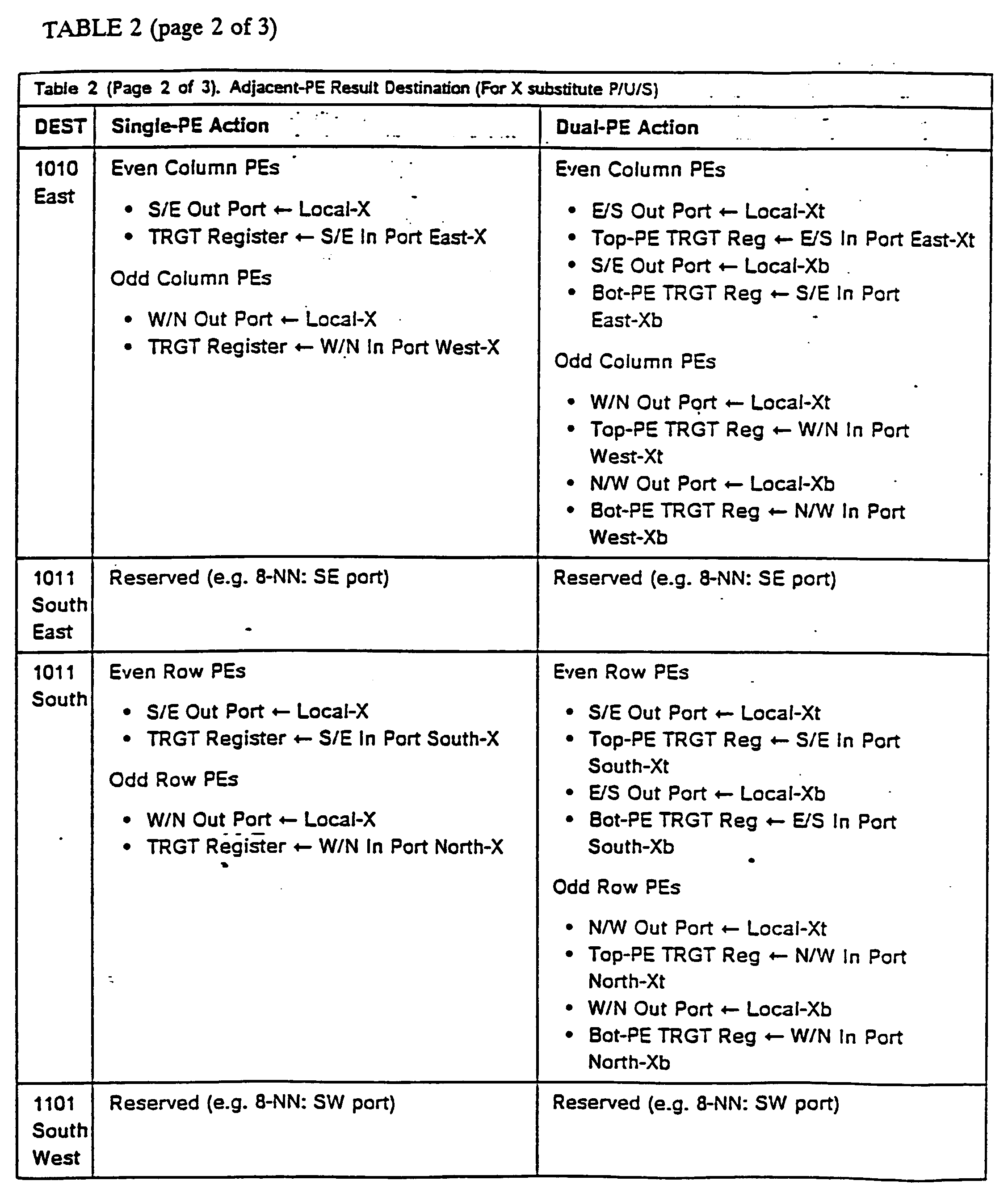
- the resulting output (P, U, and/or S) is sent to a destination register which may be in the same PE as the execution unit (a local register), in a paired-PE (in a dual-PE node), in a nearest-neighbor (NN) PE, or in an adjacent-PE.
- the destination register (Rm, Rt, and/or Rs) is specified in conjunction with the instruction's Destination (DEST) field.
- DEST Destination
- Table 1 and Table 2 list the destination (DEST) options presently defined. This field may be modified for specific instructions. For surrogate instructions only one execution unit is specified to use the nearest neighbor interface.
- a folded array 2 dimensional (2D) discrete cosine transform is prented next.
- FIG. 16 illustrates the second execution of the multiply add and DSU send surrogate.
- Fig. 17 illustrates the third execution of the multiply add and DSU send surrogate.
- Fig. 18 illustrates the fourth execution of the multiply add and DSU send surrogate.
- Fig. 19 illustrates the execution of the butterfly with the clustered processor element destination surrogate.
- Specialized Data Select Unit instructions and expansion of the direct attached destination specification to include clustered processing elements provides the zero latency communications between the clustered processing elements and the ability to pipeline across the total interconnected array.
- 8-NN NE port 1010 East • S/E Out Port ⁇ Local-X • E/S Out Port ⁇ Local-Xt • TRGT Register ⁇ W/N in Port West-X • Top-PE TRGT Reg ⁇ W/N in Port West-Xt • S/E Out Port ⁇ Local-Xb • Bot-PE TRGT Reg ⁇ N/W in Port West-Xb 1011 South East Reserved (e.g. 8-NN: SE port) Reserved (e.g.
- 8-NN SE port 1100 South • S/E Out Port ⁇ Local-X • S/E Out Port ⁇ Local-Xt • TRGT Register ⁇ W/N in Port North-X • Top-PE TRGT Reg ⁇ N/W in Port North-Xt • E/S Out Port ⁇ Local-Xb • Bot-PE TRGT Reg ⁇ W/N in Port North-Xb 1101 South West Reserved (e.g. 8-NN: SE port) Reserved (e.g.
Abstract

Description
- The invention disclosed broadly relates to data processing systems and method and more particularly relates to improvements in array processor architectures.
- It is therefore an object of the invention to provide an improved instruction driven programmable parallel processing system.
- It is another object of the invention to provide an improved parallel processing system that reduces the inherent latency in communicating between procesors.
- It is still a further object of the invention to provide an improved parallel processing system which has improved performance characteristics.
- These and other objects, features and advantages are accomplished by the invention. A plurality of processor elements (PEs) are connected in a cluster by a common instruction bus to an instruction memory. Each PE has data buses connected to at least its four nearest PE neighbors, referred to as its North, South, East and West PE neighbors. Each PE also has a general purpose register file containing several operand registers. A common instruction is broadcast from the instruction memory over the instruction bus to each PE in the cluster. The instruction includes an opcode value that controls the arithmetic or logical operation performed by an execution unit in the PE on an operand from one of the operand registers in the register file. A switch is included in each PE to interconnect it with a first PE neighbor as the destination to which the result from the execution unit is sent. In accordance with the invention, the broadcast instruction includes a destination field that controls the switch in the PE, to dynamically select the destination neighbor PE to which the result is sent. Further in acordance with the invention, the broadcast instruction includes a target field that controls the switch in the PE, to dynamically select the operand register in the register file of the PE, to which another result received from another neighbor PE in the cluster is stored. In this manner, the instruction broadcast to all the PEs in the cluster, dynamically controls the communication of operands and results between the PEs in the cluster, in a single instruction, multiple data processor array.
- Fig. 1 is a high level array machine organization diagram for multiple control units.
- Fig. 2 is an example instruction format for communications, in accordance with the invention.
- Fig. 3 is a second example instruction format for communications, in accordance with the invention.
- Fig. 4 is a single processor element (diagonal) node flow with connection interfaces.
- Fig. 5 is a dual processor element node flow with connection interfaces.
- Fig. 6 is a nearest-neighbor communication example in a single processor element node.
- Fig. 7 is a nearest-neighbor communication example in a dual processor element node.
- Fig. 8 is a logical and folded mesh representation of adjacent processor element column communications.
- Fig. 9 is a logical and folded mesh representation of adjacent processor element row communications.
- Fig. 10 is a flow organization of a processing element, depicting the flow of an individual processing element, showing all its arithmetic facilities and the points to find for connection to switch logic and paired processor elements.
- Fig. 11 is a general form diagram of the data select unit.
- Fig. 12 is an example of a data select unit in use, wherein byte B of the source is placed in the low order 8 bits of the destination register and all the remaining destination bits are forced to be the same as the sign of the byte, as performed by the data selector logic.
- Fig. 13 is a flow chart showing folded array fast odd/even symmetric 1-D DCT.
- Fig. 14 illustrates the execution of a butterfly surrogate.
- Fig. 15 illustrates the first execution of multiply add and DSU send surrogate.
- Fig. 16 illustrates the second execution of multiply add and DSU send surrogate.
- Fig. 17 illustrates the third execution of multiply add and DSU send surrogate.
- Fig. 18 illustrate the fourth execution of multiply add and DSU send surrogate.
- Fig. 19 illustrates the execution of the butterfly with a clustered processor element destination surrogate.
- Fig. 1 depicts a high level view of the Mwave array processor machine organization. The machine organization is partitioned into three main parts: the System Interfaces including
Global Memory 100 and external I/O,multiple Control Units 103 withLocal Memory 102, and the Execution Array with DistributedControl PEs 104. The System Interface is an application-dependent interface through which the Mwave array processor interfaces with Global Memory, the I/O, other system processors, and the personal computer/workstation host. Consequently, the System Interface will vary depending upon the application and the overall system design. TheControl Units 103 contain thelocal memory 102 for instruction and data storage, instruction fetch (I-Fetch) mechanisms, and operand or data fetch mechanisms (D-Fetch). The Execution Array with DistributedControl PEs 104 is a computational topology of processing elements chosen for a particular application. For example, the array may consists of N Processing Elements (PEs) 104 percontrol unit 103, with each PE containing an Instruction Buffer (IMRY) 106, a General Purpose Register File (GPRF) 108, Functional Execution units (FNS) 110, Communication Facilities (COM) 112, and interfaces to itsInstruction bus 114 and its data buses. The PEs may also contain PE-local instruction and data memories. Further, each PE contains aninstruction decode register 116 shown in Figure 4, which supports distributed control of the multiple PEs. Synchronism of local memory accessing is a cooperative process between thecontrol units 103,local memories 102, and thePEs 104. The array of PEs allows computation functions (FNS) to be executed in parallel in the PEs and results to be communicated (COM) between PEs. - With the multiple single instruction, multiple data (MSIMID) machine organization, e.g. Fig. 1, it is possible to create single or multiple thread machines wherein the topology of PEs and communication facilities can be configured for a more optimum topology depending upon the application. For example, some possible machine organizations are; multiple linear rings, a nearest neighbor 2-dimension mesh array, a folded nearest neighbor 2-dimension mesh, multiple-fold mesh, a 2-dimension hexagonal array, a folded 2-dimension hexagonal array, a folded mesh of trees, combinations of the above as well as others.
- The basic concept involved in the Mwave array processor family is that the communications of results between direct-attached processing elements can be specified in the processing element instruction set
architecture 115. In a typical RISC uni-processor, the destination of results from functional execution units is implied to be the processor's own register file breaks this "tradition", changing the definition of result destination, an implied single processor local destination, a directly-connected multiple processor destination. With this architecture and directly-connected PE-to-PE links, we can claim that communications between the directly connected PEs can be done with zero communication latency. The architecture provides this capability by including adestinatio field 120 in thesimplex instructions 115 indicating the directly-connected succeeding PE where the result target register resides, which is specified by thetarget field 126. Figure 2 shows a basic simplex 32-bit instruction 115 used in the processor, though 16-bit, 64-bit, etc. formats can use the same principle. For a four PE neighborhood, a North, East, West, and South PE destination is coded in the DestinationExtension field 120 is providing a 4-bit field here to allow for growth up to eight clustered processors (used in a three fold array) and up to an eight neighborhood array. Examples of topologies with direct-attached PEs are a nearest neighbor mesh, a folded mesh, a tree array, hypercubes, etc. It should also be appreciated that due to the clustering and nearest neighbor mesh organizations, the Physical Design process will physically place the directly connected PEs in close proximity to each other supporting short cycle times. Further, it should be appreciated that this binding of the communications destination specification in the instruction set format is done purposely to, not only provide 0-communication latency, but also to ensure hazard free communications in a SIMD array of processing elements. For explanation purposes only, the processor is used to describe the architectural details involved in implementing the described communications concept. - In the
array processor instruction 115, the Operand-1field 122, Operand-2field 124, and Targetfield 126 are register specifications and theDestination field 120 specifies the direct attached succeeding processing element to which the result is to be communicated. Theopcode field 128 specifies the arithmetic or logical operation to be performed by a selected execution unit. - In this type of SIMD array processors it is possible to tag the destination field as is shown in Figure 3, and use mode control instructions in the sequencer controller units to set the tag. The tags are then distributed to the PEs in the array. In order to change communications directions, a mode control instruction is issued prior to the execution of the instruction that communicates the result value. There are a number of implications in this approach. First, by tagging, the instruction has full use of the instruction field for function definition. Second, Tagging incurs an additional latency whenever the destination needs to be changed during communicating. If the loading of the tag register can be incorporated in a surrogate very large instruction word (VLIW), then it becomes possible to change the destination on a cycle by cycle basis. This minimizes the effect of this latency at the expense of complex control algorithms.
- The single, diagonally folded array processor Element (PE) data flow will be briefly described. The folded-array nodes are of two types: diagonal nodes containing a single Processing Element, and all other nodes which contain two PEs each. The details of each type are discussed in the following sections.
- The core logic of each folded array node is the Processing Element (PE) 104. As noted earlier, the folded array has two node types: those containing a single Processing Element and those containing dual Processing Elements. The single-PE nodes are those on the diagonal of the folded mesh; there are four such nodes in the array. The remaining six nodes contain 2 PEs each. Overall, then, there are 16 Processing Elements in the folded 4x4 array distributed among ten nodes.
- All
Processing Elements 104 in Figure 4 contain a common set of arithmetic flow components, including a fixed point/floating point Multiply/Add Unit (MAU) 110, anALU 110a, a Data Select Unit (DSU) 110b, and a General Purpose Register File (GPRF) 108 comprising 32 GPRs. EachPE 104 also contains instruction pipeline hardware. PE Decode Register (PDR) 106, instruction decode logic, and PE Execute Register (PXR) to hold instructions being executed by the PE. In addition, a small Surrogate Instruction Memory (SIM) is included in each PE to hold compound instructions which would otherwise be too complex to be contained in an instruction word. Logic around the SIM allows for loading the SIM using instructions specifically designed for that purpose. Finally, a local-PE data memory is included for each PE along with associated load and store address generation units. - This common set of flow components is augmented with different switch elements and other logic to create the single-PE node and dual-PE nodes that comprise the folded array.
- As noted above, each PE implements its own instruction pipeline logic, including instruction decode and execute registers (their abbreviated names are PDR and PXR) and instruction decode logic. One thing a PE can't do is to determine its own instruction thread (it has no Instruction Address Register and associated sequencing logic). In a machine, the Sequence Processors (SPs) or
control unit 103 serve to accomplish the instruction fetch tasks for both themselves and their associatedPEs 104. The PEs connected to a givenSP 103 are then fedinstructions 115 by theSPs 103. Theinstructions 115 are broadcast over theinstruction bus 114 to all connected PEs. EachPE 104, in turn, registers these instructions (in the PDR) and subsequently decodes and executes them. - Another part of the PE instruction pipeline flow is the Surrogate Instruction Memory, or SIM for short. SIM (which may be a combination of RAM and ROM) is included to allow the PEs to execute compound instructions (instructions which cause execute actions in multiple flow elements). Instructions of this type tend to be more complicated than ordinary instructions, and generally will require more bits to represent than are available in a single PE instruction word. In order to circumvent this restriction, a technique is proposed whereby a compound (long) instruction is represented in an instruction stream by a surrogate, or place holder instruction. Then, when the surrogate is seen in the instruction stream (by logic in the PE), a compound instruction specified by the surrogate is accessed from SIM and executed in place of the surrogate. Other logic in the PE facilitates loading compound instructions into SIM using specialized instructions. Of course, if some compound instructions are held in ROM, it is never necessary to load them. Some combination of ROM- and RAM-based SIM is probably desirable for most applications.
- The communication control is described in the following paragraphs. Fig. 4 shows the flow for a single-PE (diagonal) processing node. As shown in the figure, the node contains the full complement of components provided by a single PE 104 (MAU, ALU, DSU, GPRF, and local-PE data memory), plus switch/select logic to direct nearest-neighbor and D-bus data to and from the registers. The instruction pipeline path logic which is provided allows for orderly decoding and execution of ordinary instructions and surrogate instructions.
- The dual-PE node flow proposed for the folded-mesh array (see Fig. 5) contains all the arithmetic elements of two
PEs 104 and 104'. That is, it has 2 MAUs, 2 ALUs, 2 DSUs, 2 sets of GPRs, and 2 local-PE data memories.Switching logic 112 common to the 2 PEs allows for 4 nearest-neighbor communication paths and 2 data bus connections. The node halves (they are referred to simply as the Top and Bottom PEs) execute separate instructions, so each has its own instruction registers and decode logic. In order to facilitate communication between the two halves of the dual-PE node, multiplexors on the GPRF input ports allow load data from any source to be written into either GPRF via a transpose destination specification. - Two mode control registers are provided in each PE to control the basic operational modes in the PEs. The first mode control register contains configuration bits, I-Bus Switch, D-Bus Switch, Nearest-Neighbor/Adjacent-PE Communications Mode, and Ring/Array Mode. The second mode control register contains arithmetic options for Rounding and Saturation control of specific execution unit results. Two PE instructions control the loading of the two registers. The PE Set Mode Instruction controls the configuration bits and loads all PEs with immediate mode control information contained in the instruction. The PE Set Rounding/Saturation Instruction loads the second register.
- For the configuration mode register, the I-Bus and D-Bus switches are controlled from this mode register which specifies in the dual PEs how the two IA/IB bus ports and the two DA/DB bus ports are connected to the top and bottom PE. Using these switch settings the I-buses and D-buses can be connected to the row PEs or the column PEs. Additional mode bits indicate whether the PEs are in a Nearest Neighbor or Adjacent-PE Communications mode. Mode information must also be provided for how the PE-to-PE interface is to be used when independent row rings or column rings are used, since the nearest neighbor/Adjacent-PE interface is modified accordingly. The following lists the operational mode bit definitions.
-
- 0 =
- IA-Bus Port connects to the Top PE, IB-Bus Port connects to the Bottom PE
- 1 =
- IA-Bus Port connects to the Bottom PE, IB-Bus Port connects to the Top PE D-Bus Switch
- 0 =
- DA-Bus Port connects to the Top PE, DB-Bus Port connects to the Bottom PE
- 1 =
- DA-Bus Port connects to the Bottom PE, DB-Bus Port connects to the Top PE Nearest Neighbor/Adjacent-PE Communications Mode
- 0 =
- Nearest Neighbor Communications Enabled
- 1 =
- Adjacent-PE Communications Enabled Ring/Array Mode
- 00 =
- Row Rings: N and S Ports Disabled, E and W Ports Enabled
- 01 =
- Column Rings: E and W Ports Disabled, N and S Ports Enabled
- 10 =
- Reserved
- 11 =
- Array Mode A Load Offset Register instruction provides byte loading of the PE's offset register used in Case Surrogate instructions.
- The PE flow diagrams depicted in Fig. 4 and Fig. 5 show switches which are controlled from instructions being executed. Three types of switches are indicated in the nodes: the PE-NET Switch, Data-Bus (D-Bus) Switch, and Instruction-Bus (I-Bus) switch (only in the dual-PE node). The PE-NET switches are controlled by instructions executing in the PEs; the I-Bus and D-Bus switches are controlled by the PE-mode control register. The PEs exchange data in different ways among nodes by controlling the PE-NET switches.
- The Nearest-Neighbor (PE-NET) transmitting/receiving facilities for dual-PE nodes include four bi-directional or four input and four output driver/receiver ports. For the separate input/output port case, there is an input and output pair assigned to each nearest neighbor direction. In general, when one of these ports is assigned to transmit data to a nearest-neighbor PE, another port will also be directed to simultaneously receive data from a different PE. In the dual-PE node, Controls are provided to assure that only two of the driver/receiver ports are simultaneously transmitting data and two others are simultaneously receiving data. There are four specific cases to consider: they are Transmit East Receive West, Transmit North Receive South, Transmit South Receive North, and Transmit West Receive East. The diagonal PEs (Fig. 4) share the West/North ports and the South/East ports and thus require only two nearest-neighbor type I/O ports per diagonal PE. Note that in the dual-PE nodes, the receiving/transmitting mechanisms consist of four I/O ports.
- Fig. 6 and Fig. 7 depict the single-PE and dual-PE nodes in a less detailed form than Fig. 4 and Fig. 5 and show examples of how the nearest-neighbor ports are used in supporting four possible transmission modes. The communication modes supported cause data to be transmitted in the four cardinal directions and simultaneously received from the opposite direction. For example, transmit North and receive from the South.
- Fig. 8 and Fig. 9 depict, for a four neighborhood array, the logical representation (i.e. on the unfolded mesh) and the folded mesh representation of the four communications modes possible:
- Col-
Ring 0 -- Col-Ring 1 & Col-Ring 2 -- Col-Ring 3 Figs. 8A and 8B. - Col-
Ring 0 -- Col-Ring 3 & Col-Ring 1 -- Col-Ring 2 Fig. 8C and 8D. - Row-
Ring 0 -- Row-Ring 3 & Row-Ring 1 -- Row-Ring 2 Fig. 9C and 9D - Row-
Ring 0 -- Row-Ring 1 & Row-Ring 2 -- Row-Ring 3 Fig. 9D and 9B - The folded-array nodes each contain one or two Processing Elements as shown in Fig. 4 and Fig. 5. The PEs, which are all identical, each contain two general types of arithmetic units &dash. an ALU and a fixed point/floating point Multiply/Add Unit (MAU) &dash. a Data Selection Unit (DSU), a Local Load Data Address Generator, a Local Store Data Address Generator, and a set of 32 GPRs which serves to hold operands and working results for operations performed in the node. The register set is referred to as the General Purpose Register File, or GPRF for short. A view of the PE data flow organization, showing its individual processing elements and GPR file, is shown in Fig. 10.
- Three classes of Multiply/Add Unit MAU instructions are architectured, one for 16x16 single 32-bit fixed point results, a second for 32x32/dual-16x16 double 32-bit fixed point results, and a third for Single Precision Real Single Precision Real floating point multiply-add results. An array processor can be designed to support any one of these options and operate as subsets of the full architecture. With a 64-bit result (or double 32-bit results) the low 32-bit half uses bus Q. For an implementation with a 16x16 MAU only, the Q bus is not used. For a 32-bit Mfast processor the 32x32 MAU instructions are only able to write their results back to a local GPRF. The DEST destination field is not used in 32x32 MAU instructions and the second 32-bit result is written back to the target register specified plus one. Use of the clustered communications and nearest neighbor interface for the 32x32 MAU instructions is reserved for future machines with 64-bit Nearest Neighbor ports. Note that the Processing Element flow does not include any of the switch logic required for communication among array nodes; that logic is unique to the nodes themselves. The idea, here, is that the logic for the PE can be designed as a macro and used repeatedly to build the array. It is intended for the PE to be designed with 6 unconnected GPRF input ports, and allow these inputs to be connected in the manner appropriate for the particular node in which the PE is included. Fig. 10 indicates typical direct connections (shown in dashed lines) from the ALU, MAU, and DSU. A more complete picture of these direct connections is shown in the Single-PE node flow diagram (Fig. 4).
- The GPRF input ports may also be multiplexed as shown in the Dual-PE node flow diagram (Fig. 5 ).
- The Data Select Unit (DSU) is used in register-to-register moves and data shift operations. In the specific situation when the move destination is also the source for another move (registers are co-destinations between paired-PEs), a SWAP function can be achieved. The general form of the DSU is shown in Fig. 11 :
- The logic in the Data Selector is used to modify the data passing from source to destination for those instructions which require it. For example, when a byte is selected from the source register and then loaded into the destination in sign-extended form, the Data Selector will perform the byte-alignment and sign-extension functions. A simple example of this kind of operation is shown in Fig. 12.
- Three types of data select/move operations are provided by the Data Selector: word move, halfword move, and byte move. Within these types of moves, certain variations are supported:
- Word move
- Halfword move
- Any source halfword to any destination halfword
- Any source halfword to low half of word and:
- High halfword forced to all zeros
- High halfword forced to all ones
- High halfword forced to low halfword sign value
- Byte move
- Any source byte to any destination byte
- Any source byte to low destination byte and:
- High bytes forced to all zeros
- High bytes forced to all ones
- High bytes forced to low byte sign value
- High or low source byte pairs (b0 and bl, b2 and b3) to destination bytes bl and b3, and:
- High bytes forced to all zeros
- High bytes forced to all ones
- High bytes forced to low byte sign value
-
- When a PE execution unit performs an operations, the resulting output (P, U, and/or S) is sent to a destination register which may be in the same PE as the execution unit (a local register), in a paired-PE (in a dual-PE node), in a nearest-neighbor (NN) PE, or in an adjacent-PE. In all cases, the destination register (Rm, Rt, and/or Rs) is specified in conjunction with the instruction's Destination (DEST) field. Table 1 and Table 2 list the destination (DEST) options presently defined. This field may be modified for specific instructions. For surrogate instructions only one execution unit is specified to use the nearest neighbor interface.
- A folded
array 2 dimensional (2D) discrete cosine transform is prented next. - The signal flow graph for the symmetric discrete cosine transform (DCT) is shown in Fig. 13. Note that the outputs are scaled by the 2C(u)/N where C(u)=1/
sqrt 2 for u=0 and C(u)=1 otherwise. Note that c#x=cos(# pi/16) and that 1/(4 sqrt 2) = 1/4 c4x. - For the 2-D DCT a 1-D DCT on the columns followed by a 1-D DCT on the Rows produces the 2-D DCT result. A multiplication accumulate and register transfer via the nearest neighbor ports procedure is used. Since the butterfly results are 16-bits and the nearest neighbor ports are 32-bits both odd and even butterfly values can be sent between PEs each cycle. With dual 16x16 multipliers in each PE both odd and even parts of the 1-D DCT for 4-columns can be calculated in the same four cycles. The column 1-D DCT equations shown in Table 3. The lower case "z" in the following lists represents the column # being processed. Fig. 14 illustrates the execution of the butterfly surrogate. Fig. 15 illustrates the first execution of the multiply add and DSU send surrogate. Fig. 16 illustrates the second execution of the multiply add and DSU send surrogate. Fig. 17 illustrates the third execution of the multiply add and DSU send surrogate. Fig. 18 illustrates the fourth execution of the multiply add and DSU send surrogate. Fig. 19 illustrates the execution of the butterfly with the clustered processor element destination surrogate.
- Another 4-cycles finishes all 8-column 1-D DCTs. The scaling of the output by 1/4 is not done at this point but rather the combined scaling of 1/16 for the 2-D DCT is included in the calculation of the quantization table values. Consequently, the procedure continues with doing the 1-D DCT on the row values. First a half-word butterfly surrogate instruction creates all the row butterfly values placing the values in the pattern shown in Fig. 19 where "z", of Az through Hz, represents the row # now instead of the column #. Note that the half-word butterfly instructions send their results to the paired-PE register instead of a local register. This is a communication operation between the dual PEs used to ensure the data lines up with the coefficients.
- Az = f0z + f7z
- Bz = f1z + f6z
- Cz = f2z + f5z
- Dz = f3z + f4z
- Ez = f3z - f4z
- Fz = f2z - f5z
- Gz = f1z - f6z
- Hz = f0z - f7z
- Next a sequence of eight multiply-add-send operations are completed followed by a scaling (shift) operation to conclude the 2-D DCT. Note that the rows are done in a different order than the columns were done. With the even rows in the first set of four 32 multiplication operations followed by the odd rows in the second set of four 32 multiplications. In the first 1-D DCT columns 0-3 were done first followed by columns 4-7. The end result is the same accomplishing the 2-D DCT on the whole 8x8 array. In the JPEG and MPEG algorithms a quantization step follows the 2-D DCT, in which case the scaling step can be included in the quantization step. The total number of cycles for an 8x8 2-D DCT (excluding scaling and quantization) is 18 cycles.
- The problems and how they are solved summary:
- 1. provide a programmable low latency communication mechanism between processing elements in an array of processing elements,
- The specification of the destination of results from functional execution units is changed from always the local processor's storage (register file), to any direct attached processor's storage (register file).
- 2. pipeline across the array of processing elements,
- Due to the communication of results between processing elements with zero latency, computations can be pipelined across the array of processing elements.
- 3. communicate between clustered processing elements.
- Specialized Data Select Unit instructions and expansion of the direct attached destination specification to include clustered processing elements provides the zero latency communications between the clustered processing elements and the ability to pipeline across the total interconnected array.
- Although a specific embodiment of the invention has been disclosed, it will be understood by those having skill in the art that changes can be made to that specific embodiment without departing from the spirit and the scope of the invention.
Table 1 Nearest Neighbor Result Destination (For X substitute P/U/S) DEST Single-PE Action Dual-PE Action 0000 local GPRF Register ← X local GPRF Register ← X 0001 local GPRF Register ← X Transpose-PE GPRF Register ← X 0010 Hyper-cube Complement-PE GPRF Register ← X Hyper-cube Complement-PE GPRF Register ← X 0011 Reserved for Clustered Destinations Reserved for Clustered Destinations . . Reserved for Clustered Destinations Reserved for Clustered Destinations . 0111 Reserved for Clustered Destinations Reserved for Clustered Destinations 1000 North • W/N Out Port ← Local-X • N/W Out Port ← Local-Xt • TRGT Register ← S/E in Port South-X • Top-PE TRGT Reg ← S/E in Port South-Xt • W/N Out Port ← Local-Xb • Bot-PE TRGT Reg ← E/S in Port South-Xb 1001 North East Reserved (e.g. 8-NN: NE port) Reserved (e.g. 8-NN: NE port) 1010 East • S/E Out Port ← Local-X • E/S Out Port ← Local-Xt • TRGT Register ← W/N in Port West-X • Top-PE TRGT Reg ← W/N in Port West-Xt • S/E Out Port ← Local-Xb • Bot-PE TRGT Reg ← N/W in Port West-Xb 1011 South East Reserved (e.g. 8-NN: SE port) Reserved (e.g. 8-NN: SE port) 1100 South • S/E Out Port ← Local-X • S/E Out Port ← Local-Xt • TRGT Register ← W/N in Port North-X • Top-PE TRGT Reg ← N/W in Port North-Xt • E/S Out Port ← Local-Xb • Bot-PE TRGT Reg ← W/N in Port North-Xb 1101 South West Reserved (e.g. 8-NN: SE port) Reserved (e.g. 8-NN: SE port) 1110 West • W/N Out Port ← Local-X • W/N Out Port ← Local-Xt • TRGT Register ← S/E in Port East-X • Top-PE TRGT Reg ← E/S in Port East-Xt • N/W Out Port ← Local-Xb • Bot-PE TRGT Reg ← S/E in Port East-Xb 1111 North West Reserved (e.g. 8-NN: SE port) Reserved (e.g. 8-NN: SE port) Note: Single-PE nodes have two nearest-neighbor ports and Dual-PE nodes have four such ports. Use of these is depicted in Figure 6 on page 10 and Figure 7 on page 11 respectively. The notation Xt and Xb refers to the "top" and "bottom" PEs in a Dual-PE node shown in Figure 7 on page 11. 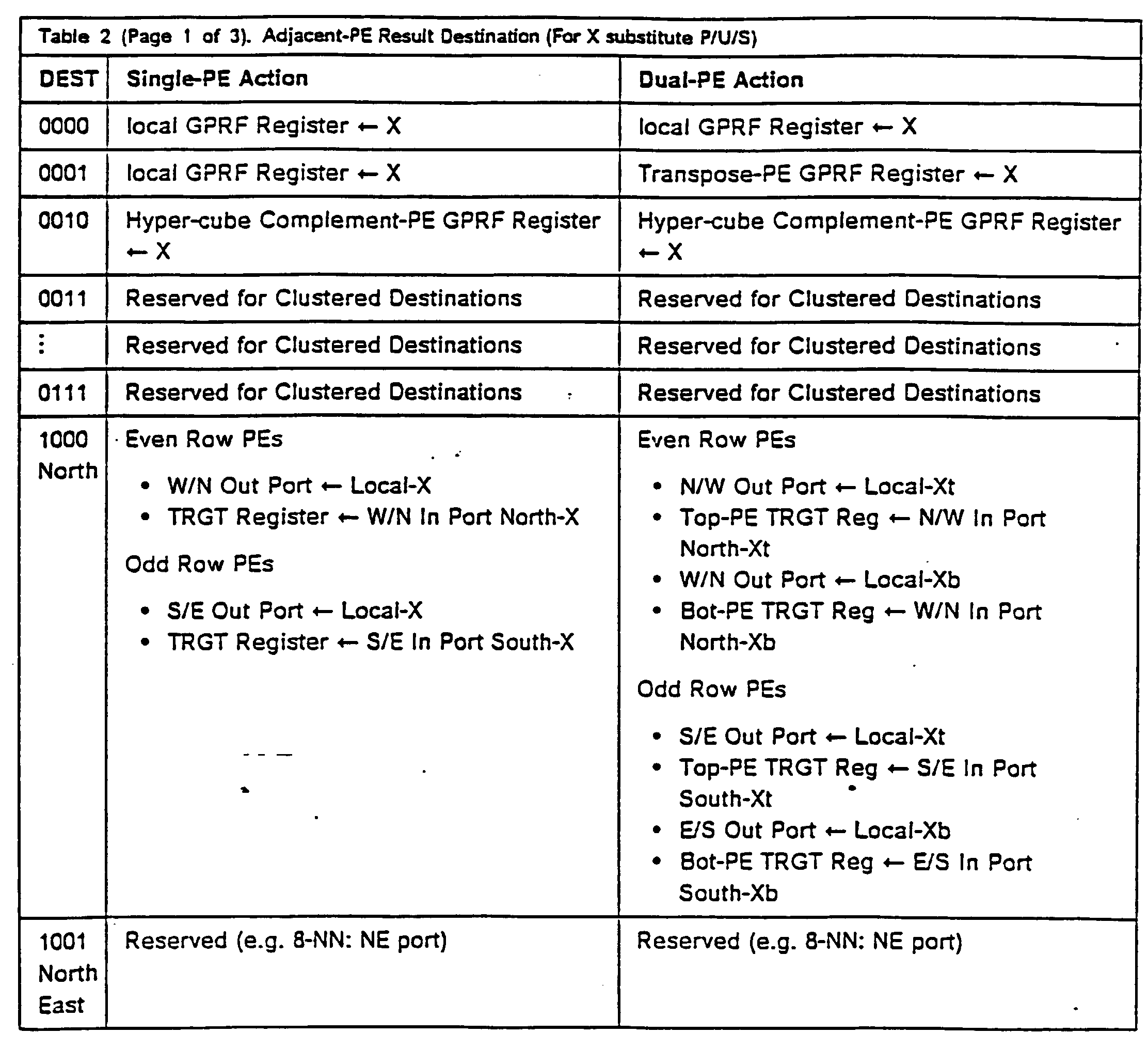

-
- Az = Pz0 + Pz7
- Bz = Pz1 + Pz6
- Cz = Pz2 + Pz5
- Dz = Pz3 + Pz4
- Ez = Pz3 - Pz4
- Fz = Pz2 - Pz5
- Gz = Pz1 - Pz6
- Hz = Pz0 - Pz7
-
- fz0-1 = Az(c4x)
- fz2-1 = Bz(c6x)
- fz4-1 = Cz(-c4x)
- fz6-1 = Dz(-c6x)
- fz1-1 = Ez(c7x)
- fz3-1 = Fz(-cx)
- fz5-1 = Gz(-cx)
- fz7-1 = Hz(c7x)
- Send (Az,Hz), (Bz,Gz), (Cz,Fz), (Dz,Ez) to South PE
-
- fz0-2 = (fz0-1 = Az(c4x)) + Dz(c4x)
- fz2-2 = (fz2-1 = Bz(c6x)) + Az(c2x)
- fz4-2 = (fz4-1 = Cz(-c4x)) + Bz(-c4x)
- fz6-2 = (fz6-1 = Dz(-c6x)) + Cz(c2x)
- fz1-2 = (fz1-1 = Ez(c7x)) + Fz(c5x)
- fz3-2 = (fz3-1 = Fz(-cx)) + Gz(-c7x)
- fz5-2 = (fz5-1 = Gz(-cx)) + Hz(c5x)
- fz7-2 = (fz7-1 = Hz(c7x)) + Ez(-cx)
- Send (Az,Hz), (Bz,Gz), (Cz,Fz), (Dz,Ez) to South PE
-
- fz0-3 = (fz0-2 = Az(c4x) + Dz(c4x)) + Cz-(c4x)
- fz2-3 = (fz2-2 = Bz(c6x) + Az(c2x)) + Dz(-c2x)
- fz4-3 = (fz4-2 = Cz(-c4x) + Bz(-c4x)) + Az(c4x)
- fz6-3 = (fz6-2 = Dz(-c6x) + Cz(c2x)) + Bz(-c2x)
- fz1-3 = (fz1-2 = Ez(c7x) + Fz(c5x)) + Gz(c3x)
- fz3-3 = (fz=3-2 = Fz(-cx) + Gz(-c7x)) + Hz(c3x)
- fz5-3 = (fz5-2 = Gz(-cx) + Hz(c5x)) + Ez(c3x)
- fz7-3 - (fz7-2 = Hz(c7x) + Ez(-cx)) + Fz(c3x)
- Send (Az,Hz), (Bz,Gz), (Cz,Fz), (Dz,Ez) to South PE
-
- fz0-4 = (fz0-3 = Az(c4x) + Dz(c4x) + Cz(c4x)) + Bz(c4x)
- fz2-4 = (fz2-3 = Bz(c6x) + Az(c2x) + Dz(-c2x)) + Cz(-c6x)
- fz4-4 = (fz4-3 = Cz(-c4x) + Bz(-c4x) + Az(c4x)) + Dz(c4x)
- fz6-4 = (fz6-3 = Dz(-c6x) + Cz(c2x) + Bz(-c2x)) + Az(c6x)
- fz1-4 = (fz1-3 = Ez(c7x) + Fz(c5x) + Gz(c3x)) + Hz(cx)
- fz3-4 = (fz3-3 = Fz(-cx) + Gz(-c7x) + Hz(c3x)) + Ez(-c5x)
- fz5-4 = fz5-3 = Gz(-cx) + Hz(c5x) + Ez(c3x)) + Fz(c7x)
- fz7-4 = fz7-3 = Hz(c7x) + Ez(-cx) + Fz(c3x)) + Gz(-c5x)
- Send (Az,Hz), (Bz,Gz), (Cz,Fz), (Dz,Ez) to South PE
Claims (5)
- A data processing system, comprising:a storage means for storing a plurality of instructions, each instruction including a first designation of a source register, a second designation of an execution unit operation, a third designation of an execution unit to output port routing, and a fourth designation of an input port to target register routing;a plurality of processing elements, each coupled by means of an instruction bus to said storage means, each of said processing elements receiving one of said instructions broadcast over said instruction bus;each of said processing elements comprising:an instruction register coupled to said instruction bus, for receiving said broadcast instruction;a register file coupled to said instruction register, said register file including a target register and a first operand register which stores a first operand;an execution unit coupled to said instruction register, said first instruction designation controlling selective coupling of said first operand register said execution unit to provide to it said first operand;said second instruction designation controlling said execution unit to execute an operation on said first operand to produce a result operand;at least a first and a second output ports having outputs respectively coupled to a first and a second succeeding ones of said processing elements;a switching means coupled to said instruction register, said third instruction designation controlling said switching means to selectively couple said execution unit to either the first output port or the second output port, to provide said result operand to the first succeeding processing element or to the second succeeding processing element, respectively;at least a first and a second input ports having inputs respectively coupled to a first and a second preceding ones of said processing elements, the first input port adapted to receive a first next operand from the first preceding processing element and the second input port adapted to receive a second next operand from the second preceding processing element; andsaid fourth instruction designation controlling said switching means to selectively couple said target register to either said first one of said input ports, to provide said first next operand to said target register or said second one of said input ports, to provide said second next operand to said target register;whereby single instruction, multiple data processing can be performed.
- The data processing system of claim 1, wherein said first succeeding processing element further comprises:a second instruction register coupled to said instruction bus, for receiving said broadcast instruction;a second register file coupled to said instruction register, said second register file including a second target register;at least two input ports, including a receiving one of which is coupled to said first output port, for receiving said result operand; anda second switching means coupled to said second instruction register, said fourth instruction designation controlling said second switching means to selectively couple said second target register to said receiving input port, to provide said result operand to said second target register;whereby single instruction, multiple data processing can be performed.
- The data processing system of claim 1 or 2, which further comprises:at least two execution units coupled to said instruction register, said first instruction designation controlling selective coupling of said first operand register said a first one of said at least two execution units to provide to it said first operand;said second instruction designation controlling said first one of said execution units to execute an operation on said first operand to produce a first result operand; andsaid third instruction designation controlling said switching means to selectively couple said first one of said execution units to either the first output port or the second output port, to provide said first result operand to the first succeeding processing element or to the second succeeding processing element, respectively.
- The data processing system of anyone of claims 1 to 3 which further comprises :
an instruction sequencing means coupled to said storage means and to said instruction bus, for fetching said instructions from said storage means and broad casting them to said plurality of processing elements. - A data processing method, comprising:retrieving a plurality of instructions, each instruction including a first designation of a source register, a second designation of an execution unit operation, a third designation of an execution unit to output port routing, and a fourth designation of an input port to target register routing;broadcasting one of said instructions to each of a plurality of processing elements;controlling with said first instruction designation, a selective coupling of a first operand register with an execution unit in each of said processing elements, to provide a first operand;controlling with said second instruction designation, said execution unit to execute an operation on said first operand to produce a result operand in each of said processing elements;controlling with said third instruction designation, a switching means in each processing element to selectively couple said execution unit to either a first output port or a second output port, to provide said result operand to a first succeeding processing element or to a second succeeding processing element, respectively; andcontrolling with said fourth instruction designation, said switching means to selectively couple a target register to either a first input port, to provide a first next operand to said target register or a second input port, to provide a second next operand to said target register;whereby single instruction, multiple data processing can be performed.
Applications Claiming Priority (2)
| Application Number | Priority Date | Filing Date | Title |
|---|---|---|---|
| US08/386,384 US5659785A (en) | 1995-02-10 | 1995-02-10 | Array processor communication architecture with broadcast processor instructions |
| US386384 | 1995-02-10 |
Publications (3)
| Publication Number | Publication Date |
|---|---|
| EP0726532A2 true EP0726532A2 (en) | 1996-08-14 |
| EP0726532A3 EP0726532A3 (en) | 1997-03-19 |
| EP0726532B1 EP0726532B1 (en) | 2000-07-26 |
Family
ID=23525370
Family Applications (1)
| Application Number | Title | Priority Date | Filing Date |
|---|---|---|---|
| EP96480018A Expired - Lifetime EP0726532B1 (en) | 1995-02-10 | 1996-02-06 | Array processor communication architecture with broadcast instructions |
Country Status (4)
| Country | Link |
|---|---|
| US (1) | US5659785A (en) |
| EP (1) | EP0726532B1 (en) |
| JP (1) | JPH0922404A (en) |
| DE (1) | DE69609430D1 (en) |
Cited By (17)
| Publication number | Priority date | Publication date | Assignee | Title |
|---|---|---|---|---|
| WO1998035299A2 (en) * | 1997-02-08 | 1998-08-13 | Pact Informationstechnologie Gmbh | Method for self-synchronization of configurable elements of a programmable component |
| EP0924625A1 (en) * | 1997-12-17 | 1999-06-23 | Hewlett-Packard Company | Configurable processor |
| US5943242A (en) * | 1995-11-17 | 1999-08-24 | Pact Gmbh | Dynamically reconfigurable data processing system |
| US6021490A (en) * | 1996-12-20 | 2000-02-01 | Pact Gmbh | Run-time reconfiguration method for programmable units |
| US6023753A (en) * | 1997-06-30 | 2000-02-08 | Billion Of Operations Per Second, Inc. | Manifold array processor |
| US6038650A (en) * | 1997-02-04 | 2000-03-14 | Pactgmbh | Method for the automatic address generation of modules within clusters comprised of a plurality of these modules |
| US6088795A (en) * | 1996-12-27 | 2000-07-11 | Pact Gmbh | Process for automatic dynamic reloading of data flow processors (DFPs) and units with two or three-dimensional programmable cell architectures (FPGAs, DPGAs and the like) |
| US6119181A (en) * | 1996-12-20 | 2000-09-12 | Pact Gmbh | I/O and memory bus system for DFPs and units with two- or multi-dimensional programmable cell architectures |
| US6167502A (en) * | 1997-10-10 | 2000-12-26 | Billions Of Operations Per Second, Inc. | Method and apparatus for manifold array processing |
| US6252792B1 (en) | 1997-01-29 | 2001-06-26 | Elixent Limited | Field programmable processor arrays |
| US6262908B1 (en) | 1997-01-29 | 2001-07-17 | Elixent Limited | Field programmable processor devices |
| US6405299B1 (en) | 1997-02-11 | 2002-06-11 | Pact Gmbh | Internal bus system for DFPS and units with two- or multi-dimensional programmable cell architectures, for managing large volumes of data with a high interconnection complexity |
| US6480937B1 (en) | 1998-02-25 | 2002-11-12 | Pact Informationstechnologie Gmbh | Method for hierarchical caching of configuration data having dataflow processors and modules having two-or multidimensional programmable cell structure (FPGAs, DPGAs, etc.)-- |
| US6523107B1 (en) | 1997-12-17 | 2003-02-18 | Elixent Limited | Method and apparatus for providing instruction streams to a processing device |
| US6567834B1 (en) | 1997-12-17 | 2003-05-20 | Elixent Limited | Implementation of multipliers in programmable arrays |
| GB2395298A (en) * | 2002-09-17 | 2004-05-19 | Micron Technology Inc | Reconfigurable multi processor array in which the result registers are selectively connected to the processing elements |
| US7996827B2 (en) * | 2001-08-16 | 2011-08-09 | Martin Vorbach | Method for the translation of programs for reconfigurable architectures |
Families Citing this family (53)
| Publication number | Priority date | Publication date | Assignee | Title |
|---|---|---|---|---|
| US7266725B2 (en) | 2001-09-03 | 2007-09-04 | Pact Xpp Technologies Ag | Method for debugging reconfigurable architectures |
| DE19651075A1 (en) | 1996-12-09 | 1998-06-10 | Pact Inf Tech Gmbh | Unit for processing numerical and logical operations, for use in processors (CPU's), multi-computer systems, data flow processors (DFP's), digital signal processors (DSP's) or the like |
| US6338106B1 (en) | 1996-12-20 | 2002-01-08 | Pact Gmbh | I/O and memory bus system for DFPS and units with two or multi-dimensional programmable cell architectures |
| JP3961028B2 (en) | 1996-12-27 | 2007-08-15 | ペーアーツェーテー イクスペーペー テクノロジーズ アクチエンゲゼルシャフト | Data flow processor (DFP) automatic dynamic unloading method and modules with 2D or 3D programmable cell structure (FPGA, DPGA, etc.) |
| US6542998B1 (en) | 1997-02-08 | 2003-04-01 | Pact Gmbh | Method of self-synchronization of configurable elements of a programmable module |
| US8686549B2 (en) * | 2001-09-03 | 2014-04-01 | Martin Vorbach | Reconfigurable elements |
| US9092595B2 (en) | 1997-10-08 | 2015-07-28 | Pact Xpp Technologies Ag | Multiprocessor having associated RAM units |
| WO1999024903A1 (en) * | 1997-11-07 | 1999-05-20 | Bops Incorporated | METHODS AND APPARATUS FOR EFFICIENT SYNCHRONOUS MIMD OPERATIONS WITH iVLIW PE-to-PE COMMUNICATION |
| DE19861088A1 (en) | 1997-12-22 | 2000-02-10 | Pact Inf Tech Gmbh | Repairing integrated circuits by replacing subassemblies with substitutes |
| US6167501A (en) * | 1998-06-05 | 2000-12-26 | Billions Of Operations Per Second, Inc. | Methods and apparatus for manarray PE-PE switch control |
| US6356994B1 (en) * | 1998-07-09 | 2002-03-12 | Bops, Incorporated | Methods and apparatus for instruction addressing in indirect VLIW processors |
| US6351807B1 (en) * | 1998-09-25 | 2002-02-26 | Bull Hn Information Systems Inc. | Data processing system utilizing multiple resister loading for fast domain switching |
| US6839728B2 (en) * | 1998-10-09 | 2005-01-04 | Pts Corporation | Efficient complex multiplication and fast fourier transform (FFT) implementation on the manarray architecture |
| US6256725B1 (en) | 1998-12-04 | 2001-07-03 | Agere Systems Guardian Corp. | Shared datapath processor utilizing stack-based and register-based storage spaces |
| US7003660B2 (en) | 2000-06-13 | 2006-02-21 | Pact Xpp Technologies Ag | Pipeline configuration unit protocols and communication |
| DE10081643D2 (en) | 1999-06-10 | 2002-05-29 | Pact Inf Tech Gmbh | Sequence partitioning on cell structures |
| US8058899B2 (en) | 2000-10-06 | 2011-11-15 | Martin Vorbach | Logic cell array and bus system |
| US7093236B2 (en) * | 2001-02-01 | 2006-08-15 | Arm Limited | Tracing out-of-order data |
| US7444531B2 (en) | 2001-03-05 | 2008-10-28 | Pact Xpp Technologies Ag | Methods and devices for treating and processing data |
| US9436631B2 (en) | 2001-03-05 | 2016-09-06 | Pact Xpp Technologies Ag | Chip including memory element storing higher level memory data on a page by page basis |
| US7844796B2 (en) | 2001-03-05 | 2010-11-30 | Martin Vorbach | Data processing device and method |
| US9037807B2 (en) | 2001-03-05 | 2015-05-19 | Pact Xpp Technologies Ag | Processor arrangement on a chip including data processing, memory, and interface elements |
| US9141390B2 (en) | 2001-03-05 | 2015-09-22 | Pact Xpp Technologies Ag | Method of processing data with an array of data processors according to application ID |
| US9250908B2 (en) | 2001-03-05 | 2016-02-02 | Pact Xpp Technologies Ag | Multi-processor bus and cache interconnection system |
| US9552047B2 (en) | 2001-03-05 | 2017-01-24 | Pact Xpp Technologies Ag | Multiprocessor having runtime adjustable clock and clock dependent power supply |
| US10031733B2 (en) | 2001-06-20 | 2018-07-24 | Scientia Sol Mentis Ag | Method for processing data |
| US7657877B2 (en) * | 2001-06-20 | 2010-02-02 | Pact Xpp Technologies Ag | Method for processing data |
| US7434191B2 (en) | 2001-09-03 | 2008-10-07 | Pact Xpp Technologies Ag | Router |
| US8686475B2 (en) * | 2001-09-19 | 2014-04-01 | Pact Xpp Technologies Ag | Reconfigurable elements |
| US20030061439A1 (en) * | 2001-09-25 | 2003-03-27 | Jeng-Jye Shau | Distributed executing units of logic integrated circuits connected to & executes on data in local data storage |
| US6968445B2 (en) * | 2001-12-20 | 2005-11-22 | Sandbridge Technologies, Inc. | Multithreaded processor with efficient processing for convergence device applications |
| EP1483682A2 (en) | 2002-01-19 | 2004-12-08 | PACT XPP Technologies AG | Reconfigurable processor |
| ATE402446T1 (en) | 2002-02-18 | 2008-08-15 | Pact Xpp Technologies Ag | BUS SYSTEMS AND RECONFIGURATION PROCEDURES |
| US9170812B2 (en) | 2002-03-21 | 2015-10-27 | Pact Xpp Technologies Ag | Data processing system having integrated pipelined array data processor |
| US8914590B2 (en) | 2002-08-07 | 2014-12-16 | Pact Xpp Technologies Ag | Data processing method and device |
| GB0215028D0 (en) * | 2002-06-28 | 2002-08-07 | Critical Blue Ltd | Microarchitecture description |
| US7657861B2 (en) | 2002-08-07 | 2010-02-02 | Pact Xpp Technologies Ag | Method and device for processing data |
| WO2005010632A2 (en) * | 2003-06-17 | 2005-02-03 | Pact Xpp Technologies Ag | Data processing device and method |
| AU2003286131A1 (en) | 2002-08-07 | 2004-03-19 | Pact Xpp Technologies Ag | Method and device for processing data |
| AU2003289844A1 (en) | 2002-09-06 | 2004-05-13 | Pact Xpp Technologies Ag | Reconfigurable sequencer structure |
| JP3987782B2 (en) * | 2002-10-11 | 2007-10-10 | Necエレクトロニクス株式会社 | Array type processor |
| US6904511B2 (en) * | 2002-10-11 | 2005-06-07 | Sandbridge Technologies, Inc. | Method and apparatus for register file port reduction in a multithreaded processor |
| US6842848B2 (en) | 2002-10-11 | 2005-01-11 | Sandbridge Technologies, Inc. | Method and apparatus for token triggered multithreading |
| US6925643B2 (en) | 2002-10-11 | 2005-08-02 | Sandbridge Technologies, Inc. | Method and apparatus for thread-based memory access in a multithreaded processor |
| EP1614030B1 (en) * | 2003-04-07 | 2015-11-04 | Koninklijke Philips N.V. | Data processing system with clustered ilp processor |
| JP4700611B2 (en) | 2003-08-28 | 2011-06-15 | ペーアーツェーテー イクスペーペー テクノロジーズ アクチエンゲゼルシャフト | Data processing apparatus and data processing method |
| JP4213750B2 (en) | 2004-08-04 | 2009-01-21 | パナソニック株式会社 | Array type arithmetic unit |
| US7506326B2 (en) * | 2005-03-07 | 2009-03-17 | International Business Machines Corporation | Method and apparatus for choosing register classes and/or instruction categories |
| US8595224B2 (en) * | 2005-09-22 | 2013-11-26 | International Business Machines Corporation | Smart path finding for file operations |
| US7818388B2 (en) * | 2005-10-07 | 2010-10-19 | International Business Machines Corporation | Data processing system, method and interconnect fabric supporting multiple planes of processing nodes |
| JP2009524134A (en) | 2006-01-18 | 2009-06-25 | ペーアーツェーテー イクスペーペー テクノロジーズ アクチエンゲゼルシャフト | Hardware definition method |
| US20140089645A1 (en) * | 2012-09-27 | 2014-03-27 | Texas Instruments Incorporated | Processor with execution unit interoperation |
| US20170116154A1 (en) * | 2015-10-23 | 2017-04-27 | The Intellisis Corporation | Register communication in a network-on-a-chip architecture |
Citations (4)
| Publication number | Priority date | Publication date | Assignee | Title |
|---|---|---|---|---|
| EP0280969A2 (en) * | 1987-03-05 | 1988-09-07 | International Business Machines Corporation | Architecture for twodimensional construction of a multidimensional array processor implementing hop command |
| EP0422964A2 (en) * | 1989-10-13 | 1991-04-17 | Texas Instruments Incorporated | Second nearest-neighbor communication network for synchronous vector processor systems and methods |
| GB2262175A (en) * | 1989-03-31 | 1993-06-09 | American Telephone & Telegraph | Reconfigurable signal processor |
| EP0602909A2 (en) * | 1992-12-18 | 1994-06-22 | Xerox Corporation | SIMD architecture with bus for transferring data to and from processing units |
Family Cites Families (10)
| Publication number | Priority date | Publication date | Assignee | Title |
|---|---|---|---|---|
| US4371931A (en) * | 1979-06-27 | 1983-02-01 | Burroughs Corporation | Linear micro-sequencer for micro-processor system utilizing specialized instruction format |
| JPS58146941A (en) * | 1982-02-26 | 1983-09-01 | Hitachi Ltd | Processor for control data of microprogram |
| JPS59174948A (en) * | 1983-03-25 | 1984-10-03 | Toshiba Corp | Information processing device |
| US5269008A (en) * | 1988-10-04 | 1993-12-07 | Mitsubishi Denki Kabushiki Kaisha | Method and apparatus for pre-processing the source of a pop instruction in a pipeline computer |
| US5218706A (en) * | 1988-12-19 | 1993-06-08 | Mitsubishi Denki Kabushiki Kaisha | Data flow processor with next destination node determination |
| US5163120A (en) * | 1989-10-13 | 1992-11-10 | Texas Instruments Incorporated | Second nearest-neighbor communication network for synchronous vector processor, systems and methods |
| JP2816248B2 (en) * | 1989-11-08 | 1998-10-27 | 株式会社日立製作所 | Data processor |
| US5218709A (en) * | 1989-12-28 | 1993-06-08 | The United States Of America As Represented By The Administrator Of The National Aeronautics And Space Administration | Special purpose parallel computer architecture for real-time control and simulation in robotic applications |
| US5201056A (en) * | 1990-05-02 | 1993-04-06 | Motorola, Inc. | RISC microprocessor architecture with multi-bit tag extended instructions for selectively attaching tag from either instruction or input data to arithmetic operation output |
| EP0486684A1 (en) * | 1990-05-22 | 1992-05-27 | International Business Machines Corporation | Virtual neurocomputer architectures for neural networks |
-
1995
- 1995-02-10 US US08/386,384 patent/US5659785A/en not_active Expired - Fee Related
-
1996
- 1996-02-06 DE DE69609430T patent/DE69609430D1/en not_active Expired - Lifetime
- 1996-02-06 EP EP96480018A patent/EP0726532B1/en not_active Expired - Lifetime
- 1996-02-08 JP JP8022362A patent/JPH0922404A/en active Pending
Patent Citations (4)
| Publication number | Priority date | Publication date | Assignee | Title |
|---|---|---|---|---|
| EP0280969A2 (en) * | 1987-03-05 | 1988-09-07 | International Business Machines Corporation | Architecture for twodimensional construction of a multidimensional array processor implementing hop command |
| GB2262175A (en) * | 1989-03-31 | 1993-06-09 | American Telephone & Telegraph | Reconfigurable signal processor |
| EP0422964A2 (en) * | 1989-10-13 | 1991-04-17 | Texas Instruments Incorporated | Second nearest-neighbor communication network for synchronous vector processor systems and methods |
| EP0602909A2 (en) * | 1992-12-18 | 1994-06-22 | Xerox Corporation | SIMD architecture with bus for transferring data to and from processing units |
Cited By (29)
| Publication number | Priority date | Publication date | Assignee | Title |
|---|---|---|---|---|
| US5943242A (en) * | 1995-11-17 | 1999-08-24 | Pact Gmbh | Dynamically reconfigurable data processing system |
| US6859869B1 (en) | 1995-11-17 | 2005-02-22 | Pact Xpp Technologies Ag | Data processing system |
| US6119181A (en) * | 1996-12-20 | 2000-09-12 | Pact Gmbh | I/O and memory bus system for DFPs and units with two- or multi-dimensional programmable cell architectures |
| US6021490A (en) * | 1996-12-20 | 2000-02-01 | Pact Gmbh | Run-time reconfiguration method for programmable units |
| US6088795A (en) * | 1996-12-27 | 2000-07-11 | Pact Gmbh | Process for automatic dynamic reloading of data flow processors (DFPs) and units with two or three-dimensional programmable cell architectures (FPGAs, DPGAs and the like) |
| US6252792B1 (en) | 1997-01-29 | 2001-06-26 | Elixent Limited | Field programmable processor arrays |
| US6262908B1 (en) | 1997-01-29 | 2001-07-17 | Elixent Limited | Field programmable processor devices |
| US6038650A (en) * | 1997-02-04 | 2000-03-14 | Pactgmbh | Method for the automatic address generation of modules within clusters comprised of a plurality of these modules |
| EP1669885A3 (en) * | 1997-02-08 | 2007-09-12 | PACT XPP Technologies AG | Method for self-synchronization of configurable elements of a programmable component |
| EP1669885A2 (en) * | 1997-02-08 | 2006-06-14 | PACT XPP Technologies AG | Method for self-synchronization of configurable elements of a programmable component |
| US6081903A (en) * | 1997-02-08 | 2000-06-27 | Pact Gmbh | Method of the self-synchronization of configurable elements of a programmable unit |
| WO1998035299A3 (en) * | 1997-02-08 | 1998-09-17 | Pact Inf Tech Gmbh | Method for self-synchronization of configurable elements of a programmable component |
| AU740243B2 (en) * | 1997-02-08 | 2001-11-01 | Pact Informationstechnologie Gmbh | Method of self-synchronization of configurable elements of a programmable component |
| WO1998035299A2 (en) * | 1997-02-08 | 1998-08-13 | Pact Informationstechnologie Gmbh | Method for self-synchronization of configurable elements of a programmable component |
| US6405299B1 (en) | 1997-02-11 | 2002-06-11 | Pact Gmbh | Internal bus system for DFPS and units with two- or multi-dimensional programmable cell architectures, for managing large volumes of data with a high interconnection complexity |
| US6338129B1 (en) | 1997-06-30 | 2002-01-08 | Bops, Inc. | Manifold array processor |
| US6023753A (en) * | 1997-06-30 | 2000-02-08 | Billion Of Operations Per Second, Inc. | Manifold array processor |
| US6167502A (en) * | 1997-10-10 | 2000-12-26 | Billions Of Operations Per Second, Inc. | Method and apparatus for manifold array processing |
| EP0924625A1 (en) * | 1997-12-17 | 1999-06-23 | Hewlett-Packard Company | Configurable processor |
| US6820188B2 (en) | 1997-12-17 | 2004-11-16 | Elixent Limited | Method and apparatus for varying instruction streams provided to a processing device using masks |
| US6567834B1 (en) | 1997-12-17 | 2003-05-20 | Elixent Limited | Implementation of multipliers in programmable arrays |
| US6523107B1 (en) | 1997-12-17 | 2003-02-18 | Elixent Limited | Method and apparatus for providing instruction streams to a processing device |
| US6571381B1 (en) | 1998-02-25 | 2003-05-27 | Pact Xpp Technologies Ag | Method for deadlock-free configuration of dataflow processors and modules with a two- or multidimensional programmable cell structure (FPGAs, DPGAs, etc.) |
| US6480937B1 (en) | 1998-02-25 | 2002-11-12 | Pact Informationstechnologie Gmbh | Method for hierarchical caching of configuration data having dataflow processors and modules having two-or multidimensional programmable cell structure (FPGAs, DPGAs, etc.)-- |
| US7996827B2 (en) * | 2001-08-16 | 2011-08-09 | Martin Vorbach | Method for the translation of programs for reconfigurable architectures |
| GB2395298A (en) * | 2002-09-17 | 2004-05-19 | Micron Technology Inc | Reconfigurable multi processor array in which the result registers are selectively connected to the processing elements |
| GB2395298B (en) * | 2002-09-17 | 2007-02-14 | Micron Technology Inc | Flexible results pipeline for processing element |
| US7627737B2 (en) | 2002-09-17 | 2009-12-01 | Micron Technology, Inc. | Processing element and method connecting registers to processing logic in a plurality of configurations |
| US8006067B2 (en) | 2002-09-17 | 2011-08-23 | Micron Technology, Inc. | Flexible results pipeline for processing element |
Also Published As
| Publication number | Publication date |
|---|---|
| EP0726532B1 (en) | 2000-07-26 |
| JPH0922404A (en) | 1997-01-21 |
| DE69609430D1 (en) | 2000-08-31 |
| US5659785A (en) | 1997-08-19 |
| EP0726532A3 (en) | 1997-03-19 |
Similar Documents
| Publication | Publication Date | Title |
|---|---|---|
| EP0726532B1 (en) | Array processor communication architecture with broadcast instructions | |
| US9460048B2 (en) | Methods and apparatus for creating and executing a packet of instructions organized according to data dependencies between adjacent instructions and utilizing networks based on adjacencies to transport data in response to execution of the instructions | |
| US6128720A (en) | Distributed processing array with component processors performing customized interpretation of instructions | |
| US6446190B1 (en) | Register file indexing methods and apparatus for providing indirect control of register addressing in a VLIW processor | |
| US5175862A (en) | Method and apparatus for a special purpose arithmetic boolean unit | |
| US7581079B2 (en) | Processor composed of memory nodes that execute memory access instructions and cooperate with execution nodes to execute function instructions | |
| US5287532A (en) | Processor elements having multi-byte structure shift register for shifting data either byte wise or bit wise with single-bit output formed at bit positions thereof spaced by one byte | |
| US6167501A (en) | Methods and apparatus for manarray PE-PE switch control | |
| US5682491A (en) | Selective processing and routing of results among processors controlled by decoding instructions using mask value derived from instruction tag and processor identifier | |
| JP3452929B2 (en) | Multiprocessor | |
| JPH0727516B2 (en) | SIMD array processor | |
| JPH07271764A (en) | Computer processor and system | |
| JP2000227858A (en) | Processor and instruction processing method therefor | |
| EP1121634A2 (en) | Forwarding paths and operand sharing in a digital signal processor | |
| JPH11212786A (en) | Data path for register base data processing and method | |
| US5481736A (en) | Computer processing element having first and second functional units accessing shared memory output port on prioritized basis | |
| US7581080B2 (en) | Method for manipulating data in a group of processing elements according to locally maintained counts | |
| US6915411B2 (en) | SIMD processor with concurrent operation of vector pointer datapath and vector computation datapath | |
| US7263543B2 (en) | Method for manipulating data in a group of processing elements to transpose the data using a memory stack | |
| US20040093484A1 (en) | Methods and apparatus for establishing port priority functions in a VLIW processor | |
| US8135940B2 (en) | Method of rotating data in a plurality of processing elements | |
| USRE41012E1 (en) | Register file indexing methods and apparatus for providing indirect control of register addressing in a VLIW processor | |
| Pechanek et al. | MFAST: a single chip highly parallel image processing architecture | |
| JPH0346068A (en) | Vector processing system | |
| CA2220993A1 (en) | Single-instruction-multiple-data processor |
Legal Events
| Date | Code | Title | Description |
|---|---|---|---|
| PUAI | Public reference made under article 153(3) epc to a published international application that has entered the european phase |
Free format text: ORIGINAL CODE: 0009012 |
|
| AK | Designated contracting states |
Kind code of ref document: A2 Designated state(s): DE FR GB |
|
| PUAL | Search report despatched |
Free format text: ORIGINAL CODE: 0009013 |
|
| AK | Designated contracting states |
Kind code of ref document: A3 Designated state(s): DE FR GB |
|
| 17P | Request for examination filed |
Effective date: 19970120 |
|
| 17Q | First examination report despatched |
Effective date: 19990412 |
|
| GRAG | Despatch of communication of intention to grant |
Free format text: ORIGINAL CODE: EPIDOS AGRA |
|
| RTI1 | Title (correction) |
Free format text: ARRAY PROCESSOR COMMUNICATION ARCHITECTURE WITH BROADCAST INSTRUCTIONS |
|
| GRAG | Despatch of communication of intention to grant |
Free format text: ORIGINAL CODE: EPIDOS AGRA |
|
| GRAH | Despatch of communication of intention to grant a patent |
Free format text: ORIGINAL CODE: EPIDOS IGRA |
|
| GRAH | Despatch of communication of intention to grant a patent |
Free format text: ORIGINAL CODE: EPIDOS IGRA |
|
| GRAA | (expected) grant |
Free format text: ORIGINAL CODE: 0009210 |
|
| AK | Designated contracting states |
Kind code of ref document: B1 Designated state(s): DE FR GB |
|
| PG25 | Lapsed in a contracting state [announced via postgrant information from national office to epo] |
Ref country code: FR Free format text: LAPSE BECAUSE OF FAILURE TO SUBMIT A TRANSLATION OF THE DESCRIPTION OR TO PAY THE FEE WITHIN THE PRESCRIBED TIME-LIMIT Effective date: 20000726 |
|
| REF | Corresponds to: |
Ref document number: 69609430 Country of ref document: DE Date of ref document: 20000831 |
|
| PG25 | Lapsed in a contracting state [announced via postgrant information from national office to epo] |
Ref country code: DE Free format text: LAPSE BECAUSE OF FAILURE TO SUBMIT A TRANSLATION OF THE DESCRIPTION OR TO PAY THE FEE WITHIN THE PRESCRIBED TIME-LIMIT Effective date: 20001027 |
|
| EN | Fr: translation not filed | ||
| PGFP | Annual fee paid to national office [announced via postgrant information from national office to epo] |
Ref country code: GB Payment date: 20010201 Year of fee payment: 6 |
|
| PLBE | No opposition filed within time limit |
Free format text: ORIGINAL CODE: 0009261 |
|
| STAA | Information on the status of an ep patent application or granted ep patent |
Free format text: STATUS: NO OPPOSITION FILED WITHIN TIME LIMIT |
|
| 26N | No opposition filed | ||
| REG | Reference to a national code |
Ref country code: GB Ref legal event code: IF02 |
|
| PG25 | Lapsed in a contracting state [announced via postgrant information from national office to epo] |
Ref country code: GB Free format text: LAPSE BECAUSE OF NON-PAYMENT OF DUE FEES Effective date: 20020206 |
|
| GBPC | Gb: european patent ceased through non-payment of renewal fee |
Effective date: 20020206 |