EP0726524A2 - Protocol and system for performing line-fill addressing during copy-back operation - Google Patents
Protocol and system for performing line-fill addressing during copy-back operation Download PDFInfo
- Publication number
- EP0726524A2 EP0726524A2 EP96480013A EP96480013A EP0726524A2 EP 0726524 A2 EP0726524 A2 EP 0726524A2 EP 96480013 A EP96480013 A EP 96480013A EP 96480013 A EP96480013 A EP 96480013A EP 0726524 A2 EP0726524 A2 EP 0726524A2
- Authority
- EP
- European Patent Office
- Prior art keywords
- address
- cache
- line
- fill
- unit
- Prior art date
- Legal status (The legal status is an assumption and is not a legal conclusion. Google has not performed a legal analysis and makes no representation as to the accuracy of the status listed.)
- Withdrawn
Links
Images

Classifications
-
- G—PHYSICS
- G06—COMPUTING; CALCULATING OR COUNTING
- G06F—ELECTRIC DIGITAL DATA PROCESSING
- G06F12/00—Accessing, addressing or allocating within memory systems or architectures
- G06F12/02—Addressing or allocation; Relocation
- G06F12/08—Addressing or allocation; Relocation in hierarchically structured memory systems, e.g. virtual memory systems
- G06F12/0802—Addressing of a memory level in which the access to the desired data or data block requires associative addressing means, e.g. caches
- G06F12/0844—Multiple simultaneous or quasi-simultaneous cache accessing
- G06F12/0855—Overlapped cache accessing, e.g. pipeline
- G06F12/0859—Overlapped cache accessing, e.g. pipeline with reload from main memory
-
- G—PHYSICS
- G06—COMPUTING; CALCULATING OR COUNTING
- G06F—ELECTRIC DIGITAL DATA PROCESSING
- G06F12/00—Accessing, addressing or allocating within memory systems or architectures
- G06F12/02—Addressing or allocation; Relocation
- G06F12/08—Addressing or allocation; Relocation in hierarchically structured memory systems, e.g. virtual memory systems
- G06F12/0802—Addressing of a memory level in which the access to the desired data or data block requires associative addressing means, e.g. caches
- G06F12/0804—Addressing of a memory level in which the access to the desired data or data block requires associative addressing means, e.g. caches with main memory updating
-
- G—PHYSICS
- G06—COMPUTING; CALCULATING OR COUNTING
- G06F—ELECTRIC DIGITAL DATA PROCESSING
- G06F12/00—Accessing, addressing or allocating within memory systems or architectures
- G06F12/02—Addressing or allocation; Relocation
- G06F12/08—Addressing or allocation; Relocation in hierarchically structured memory systems, e.g. virtual memory systems
- G06F12/0802—Addressing of a memory level in which the access to the desired data or data block requires associative addressing means, e.g. caches
- G06F12/0862—Addressing of a memory level in which the access to the desired data or data block requires associative addressing means, e.g. caches with prefetch
Definitions
- the present invention relates in general to data storage systems, more specifically, to data storage systems having a cache unit internal to the processing unit. More specifically still, the present invention relates to a memory management system in a processing system that provides next read transactions address during a write transaction.
- this caching unit is small in comparison to the larger short-term memory, it is inexpensive to add with respect to the overall cost of the computer system.
- a very large long-term storage unit is usually supplied, such as a hard disk drive, which is relatively inexpensive compared with the other types of memory.
- the primary objective of a coherent memory system is to provide the same image of memory to all devices using the system.
- Coherency allows synchronization and cooperative use of shared resources, otherwise, multiple copies of a memory location, some containing stale values, could exist in a system resulting in errors when the stale values are used.
- Each potential bus master within the system must follow rules for managing the state of its cache.
- cache coherency protocol is a coherent subset of the standard MESI four-state protocol that omits the shared state. Since data cannot be shared, the processor signals all cache block fills as if they were write misses (read-with-intent-to-modify), which flushes the corresponding copies of the data in all caches external to the processor prior to the processor's cache block fill operation.
- a protocol and system for providing a next read address during an address phase of a write transaction in a data cache unit in a processing unit includes the data cache unit and an instruction cache unit both coupled to an address bus and a data bus, respectively.
- the two buses are further connected to a system memory controller separate from the microprocessor.
- the protocol and system provide for next read address and a next transaction during an address phases in a current write transaction.
- the protocol loads a pre-fetched address within a current data transaction and then generates a next line fill addressed using the pre-fetched address which is concatenated to the current data transaction.
- the pre-fetched address is used to generate a next line fill address.
- the line fill address is generated upon determining if a cache read miss has occurred and if so, copying a modified cache line back to the main system memory and then loading the missed cache read line into the internal cache from the system memory controller.
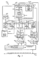
- Figure 1 depicts a block diagram of a representative microprocessor in accordance with a preferred embodiment of the present invention.
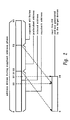
- Figure 2 is an address block generated using the present invention.
- Figure 3 depicts an example of the functional operation of the 64-bit data unit used to generate the line-fill address of Figure 2.
- FIG. 1 depicts a block diagram of a representative microprocessor 10 upon which the present invention is implemented.
- Microprocessor 10 may be selected from, for example, the family of PowerPC RISC Processors. This particular microprocessor 10 implements a 32-bit architecture, which provides 32-bit effective addresses and floating point data types of 32 and 62 bits. Significantly, the processor can issue and retire as many as three instructions per clock cycle, which instructions may be executed out-of-order for increased performance, but with completion appearing sequential for coherent and systematic operation.
- Microprocessor 10 also includes five execution units, integer unit (IU) 12 , floating point unit (FPU) 14 , branch processing unit (BPU) 16, load-store unit (LSU) 18, and system register unit (SRU) 20 .
- Microprocessor 10 also includes two physically addressed caches, one is an instruction cache 22 and the other is a data cache 24 . Both caches are two-way set associative caches.
- Two memory management units (MMUs) are further included and consist of instruction MMU 26 and data MMU 28. Both MMU s contain 64-entry two-way set associative, data and instruction translation look aside buffers (DTLB and ITLB), 30 and 32, respectively, that provide support for demand-paged virtual memory addressed translation and variable-sized block translation.
- Microprocessor 10 also supports block address translation through the use of two independent instruction and data block address translation (IBAT and DBAT) arrays 34 and 36 of four entries each. Effective addresses are compared simultaneously with all four entries in the BAT array 34 and 36 during block translation.
- Microprocessor 10 also includes a selectable multiplexed 32-bit address and 64-bit data bus 38.
- the interface protocol for microprocessor 10 allows multiple masters to compete for system resources through a central external arbiter.
- Bus 38 is connected to processor bus interface 42 , which includes a copy-back buffer 44 and a touch load buffer 46 .
- Processor bus interface 42 is further connected to the instruction cache 22 , data cache 24, and tags unit 48 and 50, which are connected to data cache 24 and instruction cache 22 , respectively.
- Instruction cache 22 is further connected to instruction unit 52 while data cache 24 is connected to the load/store unit 18. Both instruction and data caches 22 and 24 are further connected to their respective memory management units 30 and 28 via their tags unit 48 and 50. Instruction fetching and issuing is handled in instruction unit 52. Translation of address for cache or external memory accesses is handled by the MMU s 28 and 30.
- Instruction unit 52 also includes a sequential fetcher 54, instruction queue 56, dispatch unit 58 and batch processing unit 16, to provide centralized control of instruction flow to the execution units. Instruction unit 52 determines the address of the next instruction to be fetched based on information from the sequential fetcher 54 and from BPU 16 .
- Instruction unit 52 fetches instructions from instruction cache 22 into queue 56.
- BPU 16 extracts branch instructions from sequential fetcher 54 and uses static branch prediction on unresolved conditional branches to allow the instruction unit to fetch instructions from a predicted target instruction stream while a conditional branch is evaluated.
- Instruction queue 56 is designed to hold more than one instruction and can load more than one instruction from instruction unit 52 during a single cycle.
- Fetcher 54 continuously loads as many instructions as space in the instruction queue allows.
- Dispatch unit 58 performs source and destination register dependency checking, determines dispatch serializations, and inhibits subsequent instruction dispatching as required.
- FIG. 1 depicts a block diagram of a representative microprocessor 10 upon which the present invention is implemented.
- Microprocessor 10 may be selected from, for example, the family of PowerPC RISC Processors. This particular microprocessor 10 implements a 32-bit architecture, which provides 32-bit effective addresses and floating point data types of 32 and 62 bits. Significantly, the processor can issue and retire as many as three instructions per clock cycle, which instructions may be executed out-of-order for increased performance, but with completion appearing sequential for coherent and systematic operation.
- Microprocessor 10 further includes five execution units, integer unit (IU) 12 , floating point unit (FPU) 14 , branch processing unit (BPU) 16 , load-store unit (LSU) 18 , and system register unit (SRU) 20 .
- Microprocessor 10 further includes two physically addressed caches, one is an instruction cache 22 and the other is a data cache 24. Both caches are two-way set associative caches.
- Two memory management units (MMUs) are further included and consist of instruction MMU 26 and data MMU 28. Both MMU s contain 64-entry two-way set associative, data and instruction translation look aside buffers (DTLB and ITLB), 30 and 32, respectively, that provide support for demand-paged virtual memory addressed translation and variable-sized block translation.
- Microprocessor 10 also supports block address translation through the use of two independent instruction and data block address translation (IBAT and DBAT) arrays 34 and 36 of four entries each. Effective addresses are compared simultaneously with all four entries in the BAT array 34 and 36 during block translation.
- Microprocessor 10 also includes a multiplexed 32 address and 64-bit data bus 38 .
- the interface protocol for microprocessor 10 allows multiple masters to compete for system resources through a central external arbiter.
- Bus 38 is connected to processor bus interface 42, which includes a copy-back buffer 44 and a touch load buffer 46 .
- Processor bus interface 42 is further connected to the instruction cache 22, data cache 24 , and tags unit 48 and 50, which are connected to data cache 24 and instruction cache 22 , respectively.
- Instruction cache 22 is further connected to instruction unit 52 while data cache 24 is connected to the load/store unit 18 . Both instruction and data caches 22 and 24 are further connected to their respective memory manage units 30 and 28 via their tags unit 48 and 50. Instruction fetching and issuing is handled in instruction unit 52. Translation of address for cache or external memory accesses are handled by the MMU s 28 and 30 .
- Instruction unit 52 further includes a sequential fetcher 54, instruction queue 56, dispatch unit 58 and batch processing unit 16 , to provide centralized control of instruction flow to the execution units. Instruction unit 52 determines the address of the next instruction to be fetched based on information from the sequential fetcher 54 and from BPU 16.
- Instruction unit 52 fetches instructions from instruction cache 22 into queue 56.
- BPU 16 extracts branch instructions from sequential fetcher 54 and uses static branch prediction on unresolved conditional branches to allow the instruction unit to fetch instructions from a predicted target instruction stream while a conditional branch is evaluated.
- Instruction queue 56 is designed to hold more than one instruction and can load more than one instruction from instruction unit 52 during a single cycle.
- Fetcher 54 continuously loads as many instructions as space in the instruction queue allows.
- Dispatch unit 58 performs source and destination register dependency checking, determines dispatch serializations, and inhibits subsequent instruction dispatching as required.
- Branch processing unit 16 receives branch instructions from fetcher 54 performs CR lookahead operations on conditional branches to resolve them early, achieving the effect of a zero cycle branch in many cases.
- Load/store unit 18 executes all load and store instructions and provides the data transfer interface between GPRs ( nowadays?) 60 , FPRs ( nowadays?) 62 , and the cache/memory subsystem. Load/store unit 18 calculates effective addresses, performs data alignment and provides sequencing for load/store string and multiple instructions. Load and store instructions are issued and translated in program order; however, the actual memory accesses can occur out-of-order. Synchronizing instructions are provided to enforce strict ordering.
- Cacheable loads when free of data dependencies, execute any speculative manner with a maximum throughput of once per cycle and a two-cycle total latency.
- Data removed from the cache is held in rename registers 64 and 66 until completion unit 68 commits the value to a GPR or FPR.
- Stores cannot be executed speculatively and are held in the store queue until completion unit 68 signals that the store operation is to be completed to memory.
- the time required to perform the actual load or store operation varies depending on whether the operation involves the cache, system memory, or an I/O device.
- MMUs 34 and 36 support both virtual memory and physical memory for instruction and data. MMUs 34 and 36 also control access privileges for the spaces on block and page granularities.
- LSU 18 calculates effective addresses for data loads and stores, performs data alignment to and from cache memory, and provides the sequencing for load and store string and multiple word instructions.
- the instruction unit 52 calculates the effective addresses for instruction fetching.
- the higher-order bits of the effective address are translated by the appropriate MMU into physical address bits. Simultaneously, the lower-order address bits are directed to the caches where they form the index into the two-way set associative tag array. After translating the address, the MMU passes the higher-order bits of the physical address to the cache, and the cache lookup completes.
- Cache units 22 and 24 each has a line size of 32 bits in length and provides a 64-bit interface to instruction fetcher 54 and load/store unit 18, respectively.
- the surrounding logic or tags 48 and 50 select, organize, and forward the pre-requested information to the requesting unit.
- Write operation to the cache can be performed on a byte basis, and a complete read-modify-write operation to the cache can occur in each cycle.
- Both load/store unit 18 and instruction fetcher 54 provide caches 24 and 22 with the address of the data or instruction to be fetched. In the case of a cache hit, the cache returns two words to the requesting unit.
- the data cache tags 48 are single ported, simultaneous load or store and snoop accesses cause resource contention. Snoop accesses have the highest priority and are given first accesses to tags 48 , unless the snoop access coincides with a tag write, in which case the snoop is retried and must be rearbitrated for access to the cache. Load or stores that are deferred due to snoop accesses are executed on the clock cycle following the snoop.
- the present design of the caches 22 and 24 do not permit the broadcasting of the next address of the next bus transaction during the current transaction. If the system were able to broadcast the next address, or at least provide it for access during the current transaction, the system memory controller or memory management unit 28 and 30 can reduce the loss of speed in the initial memory access time of the memory outside of microprocessor unit 10 .
- a protocol is provided that uses a 32-bit address, and an 11-bit attribute, in a 64-bit data block illustrated in Figure 2. The protocol provides that the next read address transaction is available during the address phase of the current write transaction.
- the modified cache is copied back to the main system memory.
- the missed cache read line is loaded into the internal cache from main system memory.
- the address and attributes of the copy-back (write) transaction and upper address, called pre-fetched address, of the next line-fill (read) address are driven onto the system bus.
- the memory management unit or system memory controller forms the next line-fill address by concatenating the pre-fetched address with a portion of the copy-back address, called index address, as shown in Figure 2 .
- the pre-fetched address serves as the tag entry of the next line-fill.
- the index address of the copy-back is the address bits that are used to index into the internal cache, so the copy-back transaction and the line-fill transaction then share the same index value.
- the system memory controller generates the column and row address for the line-fill.
- the system memory controller can load the line-fill data into its buffers before the processor unit issues the line-fill transaction. This shortens the processor to main system memory cycle and increases the band width on the processor bus.
- the pre-fetched address is 21-bits wide and the indexed address is 6-bits wide because the internal cache is a 4 byte two-way set associative cache.
- the length of the pre-fetched and indexed address can be changed depending on the size of the internal cache. For example, an 8 byte two-way set associative cache would have a pre-fetched address of 20 bits and an indexed address of 7 bits, while a 16k two-way set associative cache would have a pre-fetched address of 19 bits and an indexed address of 8 bits.
- the 64-bit data unit in Figure 2 comprises a copy-back address that is 32-bits wide occupying the 0 - 31st bit positions.
- the indexed address is six bits wide and occupies the bit positions 22 - 27 within the copy-back address.
- the pre-fetched address is 20 bits wide and occupies bit positions 32 - 52 and is combined with the indexed address to serve as the next line-fill address, which is 28 bits wide.
- the copy-back attributes element is 11 bits wide and occupies bit positions 52 - 63.
- step 302 the system performs an internal cache read transaction. If this read transaction is a hit in the internal cache in step 304, the data is made available by the internal cache in step 306. Otherwise, if a read miss occurs, the system proceeds to step 308 . Since the processor needs to load data from system memory into the internal cache for the above read transaction, the processor has to write back from the internal cache to the system main memory the existing modified data in the internal cache to make space available for the above read transaction. Accordingly, in step 308, the system writes back all the cache contents in the processor to the system main memory.
- the system in step 310, loads the address attributes from the pre-fetched address of the next line fill address on the system bus.
- step 312 the data base portion is performed that concatenates the pre-fetched address with the indexed address value to form the next line fill address generated by the target device.
- the system memory control can take advantage of the pre-fetched addresses by loading the read data from system memory into its buffers.
- the memory controller can send the data to the processor immediately since it is already in the buffers.
Abstract
Description
- The present invention relates in general to data storage systems, more specifically, to data storage systems having a cache unit internal to the processing unit. More specifically still, the present invention relates to a memory management system in a processing system that provides next read transactions address during a write transaction.
- Many computer systems today include several levels of memory storage that attempt to fill the conflicting needs of the computer system. For example, computer systems are designed to operate very fast and memory is needed to operate at the same speed as the processing unit used within the computer system. Unfortunately, the cost of fast memory elements approach those of the cost of the microprocessor itself, thus, driving up the cost of the system overall if the fastest memory available is to be used. A compromise is to use slower but less expensive memory units for specific applications. One such application is to use slower dynamic ram memory for holding information temporarily before the processor unit needs to use it. Another alternative is to use a fast, but small and expensive, caching unit that operates at the same speed as the processing unit. Since this caching unit is small in comparison to the larger short-term memory, it is inexpensive to add with respect to the overall cost of the computer system. Lastly, a very large long-term storage unit is usually supplied, such as a hard disk drive, which is relatively inexpensive compared with the other types of memory.
- Unfortunately, having different types of memory and different sorts of memory locations causes management problems for the memory controller to maintain the most current and accurate data needed or processed by the processing unit or any other resource connected to the computing system, such as a peripheral device. Accordingly, the processing system must maintain memory coherency among the various types of memory units used.
- The primary objective of a coherent memory system is to provide the same image of memory to all devices using the system. Coherency allows synchronization and cooperative use of shared resources, otherwise, multiple copies of a memory location, some containing stale values, could exist in a system resulting in errors when the stale values are used. Each potential bus master within the system must follow rules for managing the state of its cache.
- One type of cache coherency protocol is a coherent subset of the standard MESI four-state protocol that omits the shared state. Since data cannot be shared, the processor signals all cache block fills as if they were write misses (read-with-intent-to-modify), which flushes the corresponding copies of the data in all caches external to the processor prior to the processor's cache block fill operation.
- To maintain coherency, performs a memory system read operation to the internal cache on an internal read transaction miss. Once a misses has occurred, data must be loaded from one memory system into the internal cache. Following the read transaction, then the address buffers must be loaded for a next transaction. The separation of the events of the read load and then finding the next transaction address slow down system performance.
- Accordingly, what is needed is a method for managing data in a caching memory system that is able to load next read transaction address buffers simultaneously during a system memory read transaction to internal cache in the microprocessing unit.
- It is therefore one object of the present invention to provide an improved data storage systems.
- It is another object of the present invention to provide an improved data storage systems having a cache unit internal to the processing unit.
- It is yet another object of the present invention to provide an improved memory management system in a processing system that provides next read transactions address during a write transaction.
- The foregoing objects are achieved as is now described. According to the present invention, a protocol and system for providing a next read address during an address phase of a write transaction in a data cache unit in a processing unit is disclosed. The processing unit includes the data cache unit and an instruction cache unit both coupled to an address bus and a data bus, respectively. The two buses are further connected to a system memory controller separate from the microprocessor. The protocol and system provide for next read address and a next transaction during an address phases in a current write transaction. The protocol loads a pre-fetched address within a current data transaction and then generates a next line fill addressed using the pre-fetched address which is concatenated to the current data transaction. The pre-fetched address is used to generate a next line fill address. The line fill address is generated upon determining if a cache read miss has occurred and if so, copying a modified cache line back to the main system memory and then loading the missed cache read line into the internal cache from the system memory controller.
- The above as well as additional objects, features, and avantages of the present invention will become apparent in the following detailed written description.
- The novel features believed characteristic of the invention are set forth in the appended claims. The invention itself however, as well as a preferred mode of use, further objects and advantages thereof, will best be understood by reference to the following detailed description of an illustrative embodiment when read in conjunction with the accompanying drawings, wherein:
- Figure 1 depicts a block diagram of a representative microprocessor in accordance with a preferred embodiment of the present invention.
- Figure 2 is an address block generated using the present invention.
- Figure 3 depicts an example of the functional operation of the 64-bit data unit used to generate the line-fill address of Figure 2.
- Figure 1 depicts a block diagram of a representative microprocessor 10 upon which the present invention is implemented. Microprocessor 10 may be selected from, for example, the family of PowerPC RISC Processors. This particular microprocessor 10 implements a 32-bit architecture, which provides 32-bit effective addresses and floating point data types of 32 and 62 bits. Significantly, the processor can issue and retire as many as three instructions per clock cycle, which instructions may be executed out-of-order for increased performance, but with completion appearing sequential for coherent and systematic operation.
- Microprocessor 10 also includes five execution units, integer unit (IU) 12, floating point unit (FPU) 14, branch processing unit (BPU) 16, load-store unit (LSU) 18, and system register unit (SRU) 20. Microprocessor 10 also includes two physically addressed caches, one is an
instruction cache 22 and the other is adata cache 24. Both caches are two-way set associative caches. Two memory management units (MMUs) are further included and consist ofinstruction MMU 26 and data MMU 28. Both MMUs contain 64-entry two-way set associative, data and instruction translation look aside buffers (DTLB and ITLB), 30 and 32, respectively, that provide support for demand-paged virtual memory addressed translation and variable-sized block translation. Microprocessor 10 also supports block address translation through the use of two independent instruction and data block address translation (IBAT and DBAT)arrays BAT array - Microprocessor 10 also includes a selectable multiplexed 32-bit address and 64-
bit data bus 38. The interface protocol for microprocessor 10 allows multiple masters to compete for system resources through a central external arbiter.Bus 38 is connected to processor bus interface 42, which includes a copy-back buffer 44 and atouch load buffer 46. Processor bus interface 42 is further connected to theinstruction cache 22,data cache 24, and tags unit 48 and 50, which are connected todata cache 24 andinstruction cache 22, respectively.Instruction cache 22 is further connected toinstruction unit 52 whiledata cache 24 is connected to the load/store unit 18. Both instruction anddata caches memory management units 30 and 28 via their tags unit 48 and 50. Instruction fetching and issuing is handled ininstruction unit 52. Translation of address for cache or external memory accesses is handled by theMMU s 28 and 30. -
Instruction unit 52 also includes asequential fetcher 54,instruction queue 56,dispatch unit 58 andbatch processing unit 16, to provide centralized control of instruction flow to the execution units.Instruction unit 52 determines the address of the next instruction to be fetched based on information from thesequential fetcher 54 and from BPU 16. -
Instruction unit 52 fetches instructions frominstruction cache 22 intoqueue 56.BPU 16 extracts branch instructions fromsequential fetcher 54 and uses static branch prediction on unresolved conditional branches to allow the instruction unit to fetch instructions from a predicted target instruction stream while a conditional branch is evaluated.Instruction queue 56 is designed to hold more than one instruction and can load more than one instruction frominstruction unit 52 during a single cycle.Fetcher 54 continuously loads as many instructions as space in the instruction queue allows.Dispatch unit 58 performs source and destination register dependency checking, determines dispatch serializations, and inhibits subsequent instruction dispatching as required. - Figure 1 depicts a block diagram of a representative microprocessor 10 upon which the present invention is implemented. Microprocessor 10 may be selected from, for example, the family of PowerPC RISC Processors. This particular microprocessor 10 implements a 32-bit architecture, which provides 32-bit effective addresses and floating point data types of 32 and 62 bits. Significantly, the processor can issue and retire as many as three instructions per clock cycle, which instructions may be executed out-of-order for increased performance, but with completion appearing sequential for coherent and systematic operation.
- Microprocessor 10 further includes five execution units, integer unit (IU) 12, floating point unit (FPU) 14, branch processing unit (BPU) 16, load-store unit (LSU) 18, and system register unit (SRU) 20. Microprocessor 10 further includes two physically addressed caches, one is an
instruction cache 22 and the other is adata cache 24. Both caches are two-way set associative caches. Two memory management units (MMUs) are further included and consist ofinstruction MMU 26 and data MMU 28. Both MMUs contain 64-entry two-way set associative, data and instruction translation look aside buffers (DTLB and ITLB), 30 and 32, respectively, that provide support for demand-paged virtual memory addressed translation and variable-sized block translation. Microprocessor 10 also supports block address translation through the use of two independent instruction and data block address translation (IBAT and DBAT)arrays BAT array - Microprocessor 10 also includes a multiplexed 32 address and 64-
bit data bus 38. The interface protocol for microprocessor 10 allows multiple masters to compete for system resources through a central external arbiter.Bus 38 is connected to processor bus interface 42, which includes a copy-back buffer 44 and atouch load buffer 46. Processor bus interface 42 is further connected to theinstruction cache 22,data cache 24, and tags unit 48 and 50, which are connected todata cache 24 andinstruction cache 22, respectively.Instruction cache 22 is further connected toinstruction unit 52 whiledata cache 24 is connected to the load/store unit 18. Both instruction anddata caches units 30 and 28 via their tags unit 48 and 50. Instruction fetching and issuing is handled ininstruction unit 52. Translation of address for cache or external memory accesses are handled by theMMU s 28 and 30. -
Instruction unit 52 further includes asequential fetcher 54,instruction queue 56,dispatch unit 58 andbatch processing unit 16, to provide centralized control of instruction flow to the execution units.Instruction unit 52 determines the address of the next instruction to be fetched based on information from thesequential fetcher 54 and fromBPU 16. -
Instruction unit 52 fetches instructions frominstruction cache 22 intoqueue 56.BPU 16 extracts branch instructions fromsequential fetcher 54 and uses static branch prediction on unresolved conditional branches to allow the instruction unit to fetch instructions from a predicted target instruction stream while a conditional branch is evaluated.Instruction queue 56 is designed to hold more than one instruction and can load more than one instruction frominstruction unit 52 during a single cycle.Fetcher 54 continuously loads as many instructions as space in the instruction queue allows.Dispatch unit 58 performs source and destination register dependency checking, determines dispatch serializations, and inhibits subsequent instruction dispatching as required. -
Branch processing unit 16 receives branch instructions fromfetcher 54 performs CR lookahead operations on conditional branches to resolve them early, achieving the effect of a zero cycle branch in many cases. - Load/
store unit 18 executes all load and store instructions and provides the data transfer interface between GPRs (?!?) 60, FPRs (?!?) 62, and the cache/memory subsystem. Load/store unit 18 calculates effective addresses, performs data alignment and provides sequencing for load/store string and multiple instructions. Load and store instructions are issued and translated in program order; however, the actual memory accesses can occur out-of-order. Synchronizing instructions are provided to enforce strict ordering. - Cacheable loads, when free of data dependencies, execute any speculative manner with a maximum throughput of once per cycle and a two-cycle total latency. Data removed from the cache is held in rename registers 64 and 66 until
completion unit 68 commits the value to a GPR or FPR. Stores cannot be executed speculatively and are held in the store queue untilcompletion unit 68 signals that the store operation is to be completed to memory. The time required to perform the actual load or store operation varies depending on whether the operation involves the cache, system memory, or an I/O device. -
MMUs MMUs LSU 18 calculates effective addresses for data loads and stores, performs data alignment to and from cache memory, and provides the sequencing for load and store string and multiple word instructions. Theinstruction unit 52 calculates the effective addresses for instruction fetching. - After an address is generated, the higher-order bits of the effective address are translated by the appropriate MMU into physical address bits. Simultaneously, the lower-order address bits are directed to the caches where they form the index into the two-way set associative tag array. After translating the address, the MMU passes the higher-order bits of the physical address to the cache, and the cache lookup completes.
-
Cache units instruction fetcher 54 and load/store unit 18, respectively. The surrounding logic or tags 48 and 50, select, organize, and forward the pre-requested information to the requesting unit. Write operation to the cache can be performed on a byte basis, and a complete read-modify-write operation to the cache can occur in each cycle. Both load/store unit 18 andinstruction fetcher 54 providecaches - The data cache tags 48 are single ported, simultaneous load or store and snoop accesses cause resource contention. Snoop accesses have the highest priority and are given first accesses to tags 48, unless the snoop access coincides with a tag write, in which case the snoop is retried and must be rearbitrated for access to the cache. Load or stores that are deferred due to snoop accesses are executed on the clock cycle following the snoop.
- The present design of the
caches memory management unit 28 and 30 can reduce the loss of speed in the initial memory access time of the memory outside of microprocessor unit 10. To accomplish this, a protocol is provided that uses a 32-bit address, and an 11-bit attribute, in a 64-bit data block illustrated in Figure 2. The protocol provides that the next read address transaction is available during the address phase of the current write transaction. - Specifically, during a cache transaction, such as when a cache read miss occurs at a modified cache line, the modified cache is copied back to the main system memory. Next, the missed cache read line is loaded into the internal cache from main system memory. During the copy-back address phase, the address and attributes of the copy-back (write) transaction and upper address, called pre-fetched address, of the next line-fill (read) address are driven onto the system bus. Then, during the data phase of the copy-back transaction, the memory management unit or system memory controller forms the next line-fill address by concatenating the pre-fetched address with a portion of the copy-back address, called index address, as shown in Figure 2. The pre-fetched address serves as the tag entry of the next line-fill. The index address of the copy-back is the address bits that are used to index into the internal cache, so the copy-back transaction and the line-fill transaction then share the same index value.
- The system memory controller generates the column and row address for the line-fill. Alternatively, the system memory controller can load the line-fill data into its buffers before the processor unit issues the line-fill transaction. This shortens the processor to main system memory cycle and increases the band width on the processor bus.
- In the example of Figure 2, the pre-fetched address is 21-bits wide and the indexed address is 6-bits wide because the internal cache is a 4 byte two-way set associative cache. For other designs, the length of the pre-fetched and indexed address can be changed depending on the size of the internal cache. For example, an 8 byte two-way set associative cache would have a pre-fetched address of 20 bits and an indexed address of 7 bits, while a 16k two-way set associative cache would have a pre-fetched address of 19 bits and an indexed address of 8 bits.
- The 64-bit data unit in Figure 2 comprises a copy-back address that is 32-bits wide occupying the 0 - 31st bit positions. The indexed address is six bits wide and occupies the bit positions 22 - 27 within the copy-back address. The pre-fetched address is 20 bits wide and occupies bit positions 32 - 52 and is combined with the indexed address to serve as the next line-fill address, which is 28 bits wide. Finally, the copy-back attributes element is 11 bits wide and occupies bit positions 52 - 63.
- An example of the functional operation of the 64-bit data unit used to generate the line-fill address by the target device, such as the memory controller, is depicted in the flowchart of Figure 3. In step 302, the system performs an internal cache read transaction. If this read transaction is a hit in the internal cache in
step 304, the data is made available by the internal cache instep 306. Otherwise, if a read miss occurs, the system proceeds to step 308. Since the processor needs to load data from system memory into the internal cache for the above read transaction, the processor has to write back from the internal cache to the system main memory the existing modified data in the internal cache to make space available for the above read transaction. Accordingly, instep 308, the system writes back all the cache contents in the processor to the system main memory. - During the address phrase of this write transaction, the system, in step 310, loads the address attributes from the pre-fetched address of the next line fill address on the system bus. In step 312, the data base portion is performed that concatenates the pre-fetched address with the indexed address value to form the next line fill address generated by the target device. Now that the next read transaction addresses have been provided as pre-fetch addresses, the system memory control can take advantage of the pre-fetched addresses by loading the read data from system memory into its buffers. Thus, when the processor performs the read transaction, the memory controller can send the data to the processor immediately since it is already in the buffers.
- While the invention has been particularly shown and described with reference to a preferred embodiment, it will be understood by those skilled in the art that various changes in form and detail may be made therein without departing from the spirit and scope of the invention.
Claims (10)
- In a processing unit having a data cache unit and an instruction cache unit coupled to an address bus and a data bus, which are further connected to a system memory controller outside of said microprocessor, a protocol for providing a next read address for the next transaction as provided during the address phase of a current write transaction, comprising the steps of:loading a pre-fetched address within a current data transaction; andgenerating a next line-fill address with said pre-fetched address.
- The protocol according to claim 1 wherein said step of generating said next line-fill address includes the step of:concatenating said pre-fetched address with a portion of said copy-back address.
- The protocol according to claim 2 wherein said portion of said copy-back address concatenated to said pre-fetched address is an indexed address.
- The protocol according to claim 1 further comprising the step of:generating memory column and row addresses in a main memory unit coupled to said system memory controller for line-fill.
- The protocol according to claim 1 further comprising the step of:loading said line-fill data into an instruction buffer within said processing unit before the issuance of a line-fill transaction.
- The protocol according to claim 1 before the step of generating the next line-fill address onto said system bus, including:determining if a cache read miss has occurred;if said cache read miss has occurred, copying a modified cache line back to said main unit;loading said missed cache read line into said internal cache from memory unit.
- A processing unit having a data cache unit and an instruction cache unit coupled to an address bus and a data bus, which are further connected to a system memory controller outside of said microprocessor, a system for providing a next read address for the next transaction as provided during the address phase of a current write transaction comprising:means, coupled to said cache units, for loading a pre-fetched address within a current data transaction; andmeans, coupled to said loading means, for generating a next line-fill address with said pre-fetched address.
- The system according to claim 7 wherein said means for generating said next line-fill address includes:means for concatenating said pre-fetched addresswith a portion of said copy-back address.
- The system according to claim 8 wherein said portion of said copy-back address concatenated to said pre-fetched address is an indexed address.
- The system according to claim 7 further comprising :means, coupled to said generating means, for generating memory column and row addresses in a main memory unit coupled to said system memory controller for line-fill;means, coupled to said generating means, for loading said line-fill data into an instruction buffer within said processing unit before the issuance of a line-fill transaction;means, coupled to said generating means, for determining if a cache read miss has occurred;means, coupled to said determining means, for copying a modified cache line back to said main memory unit;means, coupled to said generating means, for loading said missed cache read line into said internal cache from main memory unit.
Applications Claiming Priority (2)
| Application Number | Priority Date | Filing Date | Title |
|---|---|---|---|
| US386978 | 1995-02-10 | ||
| US08/386,978 US5687350A (en) | 1995-02-10 | 1995-02-10 | Protocol and system for performing line-fill address during copy-back operation |
Publications (2)
| Publication Number | Publication Date |
|---|---|
| EP0726524A2 true EP0726524A2 (en) | 1996-08-14 |
| EP0726524A3 EP0726524A3 (en) | 1997-10-15 |
Family
ID=23527902
Family Applications (1)
| Application Number | Title | Priority Date | Filing Date |
|---|---|---|---|
| EP96480013A Withdrawn EP0726524A3 (en) | 1995-02-10 | 1996-01-23 | Protocol and system for performing line-fill addressing during copy-back operation |
Country Status (4)
| Country | Link |
|---|---|
| US (1) | US5687350A (en) |
| EP (1) | EP0726524A3 (en) |
| JP (1) | JPH08263371A (en) |
| KR (1) | KR100218616B1 (en) |
Families Citing this family (8)
| Publication number | Priority date | Publication date | Assignee | Title |
|---|---|---|---|---|
| US7301541B2 (en) * | 1995-08-16 | 2007-11-27 | Microunity Systems Engineering, Inc. | Programmable processor and method with wide operations |
| JP3934710B2 (en) * | 1996-09-13 | 2007-06-20 | 株式会社ルネサステクノロジ | Microprocessor |
| US6065099A (en) * | 1997-08-20 | 2000-05-16 | Cypress Semiconductor Corp. | System and method for updating the data stored in a cache memory attached to an input/output system |
| US6502171B1 (en) | 1999-08-04 | 2002-12-31 | International Business Machines Corporation | Multiprocessor system bus with combined snoop responses explicitly informing snoopers to scarf data |
| US6643800B1 (en) * | 2000-02-02 | 2003-11-04 | Hewlett-Packard Development Company, L.P. | Method and apparatus for testing microarchitectural features by using tests written in microcode |
| US7797472B2 (en) * | 2004-08-25 | 2010-09-14 | Unisys Corporation | Method and apparatus for providing overlapping defer phase responses |
| US9916252B2 (en) * | 2015-05-19 | 2018-03-13 | Linear Algebra Technologies Limited | Systems and methods for addressing a cache with split-indexes |
| KR101842764B1 (en) * | 2016-03-18 | 2018-03-28 | 연세대학교 산학협력단 | Apparatus for maintaining data consistency between hardware accelerator and host system and method of the same |
Citations (3)
| Publication number | Priority date | Publication date | Assignee | Title |
|---|---|---|---|---|
| EP0432524A2 (en) * | 1989-12-13 | 1991-06-19 | International Business Machines Corporation | Cache memory architecture |
| EP0464994A2 (en) * | 1990-06-29 | 1992-01-08 | Digital Equipment Corporation | Cache memory exchange protocol |
| WO1992012484A1 (en) * | 1991-01-08 | 1992-07-23 | Ast Research, Inc. | Memory control circuit for use with a copy back cache system |
Family Cites Families (11)
| Publication number | Priority date | Publication date | Assignee | Title |
|---|---|---|---|---|
| US4084231A (en) * | 1975-12-18 | 1978-04-11 | International Business Machines Corporation | System for facilitating the copying back of data in disc and tape units of a memory hierarchial system |
| US4884197A (en) * | 1985-02-22 | 1989-11-28 | Intergraph Corporation | Method and apparatus for addressing a cache memory |
| US5148536A (en) * | 1988-07-25 | 1992-09-15 | Digital Equipment Corporation | Pipeline having an integral cache which processes cache misses and loads data in parallel |
| US5226130A (en) * | 1990-02-26 | 1993-07-06 | Nexgen Microsystems | Method and apparatus for store-into-instruction-stream detection and maintaining branch prediction cache consistency |
| US5247642A (en) * | 1990-12-05 | 1993-09-21 | Ast Research, Inc. | Apparatus for determining cacheability of a memory address to provide zero wait state operation in a computer system |
| US5353429A (en) * | 1991-03-18 | 1994-10-04 | Apple Computer, Inc. | Cache memory systems that accesses main memory without wait states during cache misses, using a state machine and address latch in the memory controller |
| GB2256512B (en) * | 1991-06-04 | 1995-03-15 | Intel Corp | Second level cache controller unit and system |
| DE4391002T1 (en) * | 1992-03-06 | 1995-02-23 | Rambus Inc | Pre-fetch into a cache to minimize memory access time and cache size in a computer system |
| US5353426A (en) * | 1992-04-29 | 1994-10-04 | Sun Microsystems, Inc. | Cache miss buffer adapted to satisfy read requests to portions of a cache fill in progress without waiting for the cache fill to complete |
| US5471602A (en) * | 1992-07-31 | 1995-11-28 | Hewlett-Packard Company | System and method of scoreboarding individual cache line segments |
| US5275216A (en) * | 1992-08-07 | 1994-01-04 | Haedt Christopher R | Liquid overflow shut-off valve |
-
1995
- 1995-02-10 US US08/386,978 patent/US5687350A/en not_active Expired - Fee Related
-
1996
- 1996-01-23 EP EP96480013A patent/EP0726524A3/en not_active Withdrawn
- 1996-01-29 KR KR1019960001881A patent/KR100218616B1/en not_active IP Right Cessation
- 1996-02-05 JP JP8018724A patent/JPH08263371A/en active Pending
Patent Citations (3)
| Publication number | Priority date | Publication date | Assignee | Title |
|---|---|---|---|---|
| EP0432524A2 (en) * | 1989-12-13 | 1991-06-19 | International Business Machines Corporation | Cache memory architecture |
| EP0464994A2 (en) * | 1990-06-29 | 1992-01-08 | Digital Equipment Corporation | Cache memory exchange protocol |
| WO1992012484A1 (en) * | 1991-01-08 | 1992-07-23 | Ast Research, Inc. | Memory control circuit for use with a copy back cache system |
Also Published As
| Publication number | Publication date |
|---|---|
| EP0726524A3 (en) | 1997-10-15 |
| JPH08263371A (en) | 1996-10-11 |
| KR100218616B1 (en) | 1999-09-01 |
| KR960032191A (en) | 1996-09-17 |
| US5687350A (en) | 1997-11-11 |
Similar Documents
| Publication | Publication Date | Title |
|---|---|---|
| US5893921A (en) | Method for maintaining memory coherency in a computer system having a cache utilizing snoop address injection during a read transaction by a dual memory bus controller | |
| US5249286A (en) | Selectively locking memory locations within a microprocessor's on-chip cache | |
| US5511175A (en) | Method an apparatus for store-into-instruction-stream detection and maintaining branch prediction cache consistency | |
| US6119204A (en) | Data processing system and method for maintaining translation lookaside buffer TLB coherency without enforcing complete instruction serialization | |
| US6523109B1 (en) | Store queue multimatch detection | |
| US5944815A (en) | Microprocessor configured to execute a prefetch instruction including an access count field defining an expected number of access | |
| US6119205A (en) | Speculative cache line write backs to avoid hotspots | |
| US6212602B1 (en) | Cache tag caching | |
| US5793941A (en) | On-chip primary cache testing circuit and test method | |
| US6216200B1 (en) | Address queue | |
| US6425075B1 (en) | Branch prediction device with two levels of branch prediction cache | |
| US5778407A (en) | Methods and apparatus for determining operating characteristics of a memory element based on its physical location | |
| US6173393B1 (en) | System for writing select non-contiguous bytes of data with single instruction having operand identifying byte mask corresponding to respective blocks of packed data | |
| US6122709A (en) | Cache with reduced tag information storage | |
| US5897655A (en) | System and method for cache replacement within a cache set based on valid, modified or least recently used status in order of preference | |
| EP1278125A2 (en) | Indexing and multiplexing of interleaved cache memory arrays | |
| US20040111561A1 (en) | System and method for managing a cache memory | |
| KR20030010727A (en) | A translation lookaside buffer flush filter | |
| JPH02234248A (en) | Processing of memory access exception by instruction fetched previously within instruction pipeline of digital computer with virtual memory system as base | |
| JP2735781B2 (en) | Cache memory control system and method | |
| US20030074530A1 (en) | Load/store unit with fast memory data access mechanism | |
| US5649137A (en) | Method and apparatus for store-into-instruction-stream detection and maintaining branch prediction cache consistency | |
| JPH06236353A (en) | Method and system for increase of parallelism of system memory of multiprocessor computer system | |
| US6446189B1 (en) | Computer system including a novel address translation mechanism | |
| US5550995A (en) | Memory cache with automatic alliased entry invalidation and method of operation |
Legal Events
| Date | Code | Title | Description |
|---|---|---|---|
| PUAI | Public reference made under article 153(3) epc to a published international application that has entered the european phase |
Free format text: ORIGINAL CODE: 0009012 |
|
| AK | Designated contracting states |
Kind code of ref document: A2 Designated state(s): DE FR GB |
|
| 17P | Request for examination filed |
Effective date: 19970120 |
|
| PUAL | Search report despatched |
Free format text: ORIGINAL CODE: 0009013 |
|
| AK | Designated contracting states |
Kind code of ref document: A3 Designated state(s): DE FR GB |
|
| 17Q | First examination report despatched |
Effective date: 20000511 |
|
| STAA | Information on the status of an ep patent application or granted ep patent |
Free format text: STATUS: THE APPLICATION IS DEEMED TO BE WITHDRAWN |
|
| 18D | Application deemed to be withdrawn |
Effective date: 20000801 |