EP0725416A1 - Method for making a pillar structure for field emission devices - Google Patents
Method for making a pillar structure for field emission devices Download PDFInfo
- Publication number
- EP0725416A1 EP0725416A1 EP96300478A EP96300478A EP0725416A1 EP 0725416 A1 EP0725416 A1 EP 0725416A1 EP 96300478 A EP96300478 A EP 96300478A EP 96300478 A EP96300478 A EP 96300478A EP 0725416 A1 EP0725416 A1 EP 0725416A1
- Authority
- EP
- European Patent Office
- Prior art keywords
- pillars
- electrodes
- pillar
- voltage
- composite
- Prior art date
- Legal status (The legal status is an assumption and is not a legal conclusion. Google has not performed a legal analysis and makes no representation as to the accuracy of the status listed.)
- Granted
Links
Images

Classifications
-
- H—ELECTRICITY
- H01—ELECTRIC ELEMENTS
- H01J—ELECTRIC DISCHARGE TUBES OR DISCHARGE LAMPS
- H01J9/00—Apparatus or processes specially adapted for the manufacture, installation, removal, maintenance of electric discharge tubes, discharge lamps, or parts thereof; Recovery of material from discharge tubes or lamps
- H01J9/24—Manufacture or joining of vessels, leading-in conductors or bases
- H01J9/241—Manufacture or joining of vessels, leading-in conductors or bases the vessel being for a flat panel display
- H01J9/242—Spacers between faceplate and backplate
-
- H—ELECTRICITY
- H01—ELECTRIC ELEMENTS
- H01J—ELECTRIC DISCHARGE TUBES OR DISCHARGE LAMPS
- H01J31/00—Cathode ray tubes; Electron beam tubes
- H01J31/08—Cathode ray tubes; Electron beam tubes having a screen on or from which an image or pattern is formed, picked up, converted, or stored
- H01J31/10—Image or pattern display tubes, i.e. having electrical input and optical output; Flying-spot tubes for scanning purposes
- H01J31/12—Image or pattern display tubes, i.e. having electrical input and optical output; Flying-spot tubes for scanning purposes with luminescent screen
- H01J31/123—Flat display tubes
-
- H—ELECTRICITY
- H01—ELECTRIC ELEMENTS
- H01J—ELECTRIC DISCHARGE TUBES OR DISCHARGE LAMPS
- H01J2329/00—Electron emission display panels, e.g. field emission display panels
- H01J2329/86—Vessels
- H01J2329/8625—Spacing members
- H01J2329/863—Spacing members characterised by the form or structure
-
- H—ELECTRICITY
- H01—ELECTRIC ELEMENTS
- H01J—ELECTRIC DISCHARGE TUBES OR DISCHARGE LAMPS
- H01J2329/00—Electron emission display panels, e.g. field emission display panels
- H01J2329/86—Vessels
- H01J2329/8625—Spacing members
- H01J2329/863—Spacing members characterised by the form or structure
- H01J2329/8635—Spacing members characterised by the form or structure having a corrugated lateral surface
-
- H—ELECTRICITY
- H01—ELECTRIC ELEMENTS
- H01J—ELECTRIC DISCHARGE TUBES OR DISCHARGE LAMPS
- H01J2329/00—Electron emission display panels, e.g. field emission display panels
- H01J2329/86—Vessels
- H01J2329/8625—Spacing members
- H01J2329/864—Spacing members characterised by the material
Definitions
- This invention pertains to field emission devices and, in particular, to methods for preparing an improved pillar structure for such devices using a multi-layer material configuration.
- Field emission of electrons into vacuum from suitable cathode materials is currently the most promising source of electrons in vacuum devices.
- These devices include flat panel displays, klystrons and traveling wave tubes used in microwave power amplifiers, ion guns, electron beam lithography, high energy accelerators, free electron lasers, and electron microscopes and microprobes.
- the most promising application is the use of field emitters in thin matrix-addressed flat panel displays. See, for example, J. A. Costellano, Handbook of Display Technology , Academic Press, New York, pp. 254 (1992), which is incorporated herein by reference.
- Diamond is a desirable material for field emitters because of its low-voltage emission characteristics and its robust mechanical and chemical properties.
- Field emission devices employing diamond field emitters are disclosed, for example, U.S. Patent application Serial No. 08/361616 filed by Jin et al. December 22, 1994. This application is incorporated herein by reference.
- a typical field emission device comprises a cathode including a plurality of field emitter tips and an anode spaced from the cathode.
- a voltage applied between the anode and cathode induces the emission of electrons towards the anode.
- a conventional electron field emission flat panel display comprises a flat vacuum cell having a matrix array of microscopic field emitters formed on a cathode of the cell ( the back plate ) and a phosphor coated anode on a transparent front plate. Between cathode and anode is a conductive element called a grid or gate .
- the cathodes and gates are typically intersecting strips (usually perpendicular strips) whose intersections define pixels for the display.
- a given pixel is activated by applying voltage between the cathode conductor strip and the gate conductor. A more positive voltage is applied to the anode in order to impart a relatively high energy (400-3,000 eV) to the emitted electrons. See, for example, United States Patents Nos. 4,940,916; 5,129,850; 5,138,237 and 5,283,500, each of which is incorporated herein by reference.
- the anode layer is mechanically supported and electrically separated from the cathode by pillars placed sparsely so as not to drastically reduce the field emission areas of the display.
- the pillar material In order to withstand the high voltage applied to the anode for phosphor excitation, the pillar material should be dielectric and should have high breakdown voltage.
- FED field emission display
- the measured efficiency for typical ZnS-based phosphor increases approximately as the square-root of the voltage over a wide voltage range, so a field emission display should be operated at as high a voltage as possible to obtain maximum efficiency. This is especially important for portable, battery-operated devices in which low power consumption is desirable.
- the applicants have also found that the electron dose that phosphors can survive without substantial degradation of their luminous output similarly increases with operating voltage. It is not generally recognized that the combination of these two effects makes it especially advantageous to operate at high voltage.
- the display needs to produce the same light output, irrespective of its operating voltage. Since the efficiency improves at high voltage, less total power must be deposited on the anode. Further, since the power is the anode voltage times the current, the current required to maintain a constant light output decreases even faster than the power. When this is combined with the above-mentioned increase in dose required to damage the phosphor, the lifetime is found to be a strongly increasing function of the voltage. For a typical phosphor, we anticipate that changing the operating voltage from 500V to 5000V would increase the device's operating lifetime by a factor of 100.
- pillars Most practical field emission displays require integrated dielectric pillars to keep the substrate and screen separated. Without these pillars, the pressure difference between a normal atmosphere outside and vacuum inside will flex the anode and the cathode surfaces together.
- the pillars would be typically 100-1000 ⁇ m high, and would support the area of typically 1000 - 100,000 pixels. Because of the insulator breakdown in high electrical fields, these pillars put limitations on the voltage that can be applied to the display, and consequently limit the phosphor efficiency and thus the power consumption. The voltage limitation arises because it is necessary to avoid electric discharges along the surface of the pillars.
- the insulator surface will generally become charged. The sign of the charge is not necessarily negative. Incoming electrons can knock electrons off the insulator, a process known as secondary emission. If, on average, there is more than one outgoing electron per incoming electron, the insulator will actually charge positively. The positive charge can then attract more electrons. This process doesn't run away on an isolated block of insulator, because the positive charge eventually prevents the secondary electrons from leaving, and the system reaches equilibrium.
- the secondary electrons can always hop toward the more positive electrode.
- These stronger gradients can lead to field emission from the negative electrode, and another cycle of charging and emission. This process can lead to the formation of an arc across the surface long before the insulator would break down through the bulk.
- a pillar structure has a substantially longer surface path length from negative to positive electrodes to resist breakdown in a high voltage environment.
- the processing and assembly methods permit low-cost manufacturing of high breakdown-voltage, dielectric pillars for the flat panel display.
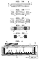
- FIG. 1 is a drawing describing the relationship between material properties and allowable geometry of the pillar.
- FIG. 2 is a block diagram of the steps in a method of making an improved pillar structure using a multilayer matrix.
- FIG. 3 schematically illustrates the steps in FIG. 2 with cross-sectional diagrams.
- FIG. 4 is a schematic diagram of a field emission flat panel display device employing the pillars of this invention.
- the pillars in the field emission flat panel displays mechanically support the anode layer above the pillars, and electrically separate the cathode and anode. Therefore, mechanical strength as well as dielectric properties of the pillar material are important.
- the pillar material In order to withstand the high electrical field applied to operate the phosphor material which is typically coated on the anode plate, the pillar material should be an electrical insulator with high breakdown voltage, e.g. greater than about 2000 V and preferably greater than 4000 V for using the established phosphors such as the ZnS:Cu,Al phosphor.
- the optimal pillar design is one where surface paths from negative to positive electrodes are as long as possible, while keeping the height of the pillar short.
- the pillar it is desirable to construct the pillar so that most secondary electrons will re-impact the pillar surface close to the point of their generation, rather than being accelerated a substantial distance toward the positive electrode.
- This goal is advantageous because most materials generate less than one secondary electron for each incident electron if the incident energy is less than 500V (or more preferably, less than 200V). Under these conditions, secondary electrons will generally not have enough energy to make an increasing number of secondaries of their own.
- "close” is defined as "a point where the electrostatic potential is less than 500V more positive than the point at which the electron is generated, and preferably less than 200V more positive.”
- the pillar must not be so much wider at the anode end so that it substantially reduces the area that can be allocated to the phosphor screen.
- a suitable pillar material according to the invention may be chosen from glasses such as lime glass, Pyrex, fused quartz, ceramic materials such as oxide, nitride, oxynitride, carbide (e.g., Al 2 O 3 , TiO 2 , ZrO 2 , AlN) or their mixture, polymers (e.g., polyimide resin) or composites of ceramics, polymers, or metals.
- the preferred pillar material is 70 wt% portland cement, 30% alumina, though other castable refractory ceramics are appropriate (ORPAC castable ceramic pastes).
- a typical geometry of the pillar in this invention is a modified form of either a round or rectangular rod.
- a cylinder, plate, or other irregular shapes can also be used as a basis of this invention.
- the diameter of the pillar is typically 50-1000 ⁇ m, and preferably 100-300 ⁇ m.
- the height-to-diameter aspect ratio of the pillar is typically in the range of 1-10, preferably in the range of 2-5.
- the desired number or density of the pillars is dependent on various factors to be considered. For sufficient mechanical support of the anode plate, a larger number of pillars is desirable. However, in order to minimize the loss of display quality, manufacturing costs and risk of electrical breakdown, too many pillars are not desirable, and hence, some compromise is necessary.
- a typical density of the pillar in this invention is about 0.01-2% of the total display surface area, and preferably 0.05-0.5%. For a FED display of about 25x25 cm area, approximately 500-2000 pillars each with a cross-sectional area of 100x100 ⁇ m is a good example of the pillar structure.
- the surface length of the pillar between the cathode and the anode is increased by introducing essentially a circumferentially undulating surface structure in the pillar material through novel processing. This structure also traps many secondary electrons, and thus further improves the breakdown voltage.
- ⁇ max and the conductivity there is an allowable tradeoff between the material properties (i.e. ⁇ max and the conductivity) and the geometry of the pillars.
- ⁇ max and the conductivity the material properties
- the geometry of the pillars In order to reduce the undesirable multiplication of electrons, it is desirable that the average number of secondary electrons that are generated by an incident electron and then travel through enough of a potential drop to generate more than one tertiary electron be less than unity.
- a tertiary electron as another secondary electron produced from a initial secondary electron that has been accelerated into a surface.
- the former secondary electron typically must have 200-1000 eV of energy on impact with the surface in order to generate more than one tertiary electron. This threshold energy is referred to as E o , and is available in standard tables for each material.
- FIG. 1 which illustrates a pillar 10 having a groove 11 not all secondary electrons 12 will travel far enough to have gained more energy than E o so that they will make more than one tertiary electron 13.
- Surfaces with deep grooves are preferred, and surfaces where the groove depth is greater than the width are especially preferred, because a large fraction of secondary electrons collide with the surface before they have acquired much energy. Consequently, materials with higher ⁇ max require grooves with a greater ratio of d/w.
- the voltage difference across a groove must be smaller than E o /q (q is the electron charge), for the above argument to hold. Consequently, the desired number of grooves along the length of the pillar according to the invention, is typically greater than Vq/E o , and preferably greater than 2Vq/E o .
- pillars with large E o require fewer grooves.
- the first step (block A in FIG. 2) is preparation of a disposable multi-layer composite consisting of two or more materials with differential dissolution rate in acid, alkali, or solvent, or with differential a degree of swelling in the presence of solvent.
- the two or more different materials are stacked in an alternating sequence.
- Well-known dispensing techniques such as spray coating, spin coating, doctor blading can be used for constructing a multi-layer polymer composite.
- FIG. 3A shows the resulting structure 30 with different layers 31 and 32.
- the preferred embodiment to obtain a multilayer is co-extrusion from the melt, with lay up of several co-extruded sheets as necessary to reach the desired thickness.
- Co-extrusion is a well established technique in the food packaging industry.
- the co-extruded polymers must be matched in melt flow properties, typically by choice of materials and by adjusting the distribution of molecular weights.
- alternate layers of the polymer could be sprayed or rollcoated onto films of the other layers, then the resulting bilayer sheets can be pressed together to make the final multilayer film.
- This multilayer film can be adhered onto the emitter structure, e.g., by heating the assembly to 50-150°C for improved adhesion.
- the film according to the invention is typically about 0.1-2.0 mm thick, and preferably 0.3-1.0 mm thick.
- Yet another alternative is to directly deposit the multilayers onto the substrate by spin-coating or spray-coating of the two or more polymer precursor liquids with intermediate or final drying/solidification/polymerization steps.
- the polymers are chosen to have solubilities (in a suitable etchant) or swelling rates alternatively above and below a smoothly nondecreasing curve. Polymer layers closer to the substrate are exposed to the etchant (solvent) for less time, so they preferably etch)swell) more rapidly so that the final etched hole has dimensions near the substrate similar to its dimensions near the free surface.
- the next step in FIG. 2 is to make vertical cavities, in the multi-layer composite sheet.
- the cavities having the size of the desired pillar dimension are either cut out, punched out, or embossed mechanically, or thermally cut out (e.g., by excimer laser ablation), or chemically etched out (e.g., photolithographically or by using differentially photo-sensitive polymers as the components in the multilayer composite).
- the preferred method is mechanical embossing.
- FIG. 3B shows a multilayer composite 30 with cavities 33 after an embossing tool penetrated the film. Typical depths are 90%-99%, preferably 97%-99%.
- the next step in FIG. 2 is then to create a grooved wall in the cavities, as schematically illustrated in FIG. 3C (cavities 33) by utilizing the differential etch rate or differential swelling of the two materials in the multilayer structure.
- the alternate layers are poly(methyl methacrylate) and a novolac resin, or any other resin containing acidic functional groups.
- Such resin can be typically etched in aqueous alkali solutions.
- One skilled in the art can choose appropriate functional groups, functional group densities, and molecular weight distributions to tailor the etch rates to the desired values.
- polymers with amine functional groups can be alternated with the poly(methyl methacrylate), then etched in aqueous acid.
- a second alternate would utilize polystyrene, which may be controllably swollen by application of methylated benzene compounds or similar low vapor presume solvents.
- An oxygen plasma exposure may be briefly used to clean the surface to improve adhesion of the pillars.
- the grooved cavity is then filled with dielectric material (e.g., glass or cement slurry.
- dielectric material e.g., glass or cement slurry.
- the structure is illustrated in FIG. 3D with castables 34 in place. The process may be repeated if necessary to completely fill the cavities with the dielectric pillar material.
- the next step in FIG. 2 (block E) is to remove the matrix multilayer composite material to free the cast grooved pillars 35.
- solvents may be used to dissolve the multilayer although controlled pyrolysis and/or oxidation may be used if the substrate is compatible, though aqueous etchants are contemplated.
- the process illustrated by FIGS. 2 and 4 can be applied to either a free-standing composite layer matrix or to a composite matrix adhered to the display substrate. If it is carried out as a free standing composite, the resultant pillars maybe picked and placed on the display substrate, preferably in a simultaneous manner (all pillars together) or partly simultaneous manner (e.g., one row at a time) using vacuum suction template, tacky template, or multi-pronged robotic pick-and-place apparatus.
- a simultaneous manner all pillars together
- partly simultaneous manner e.g., one row at a time
- vacuum suction template tacky template
- multi-pronged robotic pick-and-place apparatus we anticipate that it will be necessary to adjust the size of free-standing films by tensioning under computer control to improve the registration between the pillars and the desired locations on the substrate.
- the conductor coating e.g., the gate film or other conductive layers on the display substrate
- the dielectric materials undesifacts during the heat treatment or chemical etching processes involved.
- FIG. 4 is a schematic cross section of an exemplary flat panel display 90 using the high breakdown voltage pillars 96 according to the present invention.
- the display comprises a cathode 91 including a plurality of emitters 92 and an anode 93 disposed in spaced relation from the emitters within a vacuum seal.
- the anode conductor 93 formed on a transparent insulating substrate 94 is provided with a phosphor layer 95 and mounted on support pillars 96.
- a perforated conductive gate layer 97 Between the cathode and the anode and closely spaced from the emitters.
- the space between the anode and the emitter is sealed and evacuated, and voltage is applied by power supply 98.
- the field-emitted electrons from electron emitters 92 are accelerated by the gate electrode 97 from multiple emitters 92 on each pixel and move toward the anode conductive layer 93 (typically transparent conductor such as indium-tin-oxide or a predominantly open grid-like structure, with the phosphor disposed in the open areas of the grid) coated on the anode substrate 94.
- Phosphor layer 95 is disposed between the electron emitters and the anode. As the accelerated electrons hit the phosphor, a display image is generated.
- the above-described embodiments are illustrative of only a few of the many possible specific embodiments which can represent applications of the principles of the invention.
- the high breakdown voltage pillars of this invention can be used not only for flat-panel display apparatus but for other applications, such as a x-y matrix addressable electron sources for electron lithography or for microwave power amplifier tubes.
Landscapes
- Engineering & Computer Science (AREA)
- Manufacturing & Machinery (AREA)
- Cathode-Ray Tubes And Fluorescent Screens For Display (AREA)
- Vessels, Lead-In Wires, Accessory Apparatuses For Cathode-Ray Tubes (AREA)
- Manufacture Of Electron Tubes, Discharge Lamp Vessels, Lead-In Wires, And The Like (AREA)
- Cold Cathode And The Manufacture (AREA)
Abstract
providing said electrodes;
forming a mold having grooved wall cavities;
molding dielectric pillars in said cavities, said pillars having grooved outer surfaces;
adhering said pillars to one of said electrodes; and
finishing said device.
Description
- This invention pertains to field emission devices and, in particular, to methods for preparing an improved pillar structure for such devices using a multi-layer material configuration.
- Field emission of electrons into vacuum from suitable cathode materials is currently the most promising source of electrons in vacuum devices. These devices include flat panel displays, klystrons and traveling wave tubes used in microwave power amplifiers, ion guns, electron beam lithography, high energy accelerators, free electron lasers, and electron microscopes and microprobes. The most promising application is the use of field emitters in thin matrix-addressed flat panel displays. See, for example, J. A. Costellano, Handbook of Display Technology, Academic Press, New York, pp. 254 (1992), which is incorporated herein by reference. Diamond is a desirable material for field emitters because of its low-voltage emission characteristics and its robust mechanical and chemical properties. Field emission devices employing diamond field emitters are disclosed, for example, U.S. Patent application Serial No. 08/361616 filed by Jin et al. December 22, 1994. This application is incorporated herein by reference.
- A typical field emission device comprises a cathode including a plurality of field emitter tips and an anode spaced from the cathode. A voltage applied between the anode and cathode induces the emission of electrons towards the anode.
- A conventional electron field emission flat panel display comprises a flat vacuum cell having a matrix array of microscopic field emitters formed on a cathode of the cell ( the back plate ) and a phosphor coated anode on a transparent front plate. Between cathode and anode is a conductive element called a grid or gate . The cathodes and gates are typically intersecting strips (usually perpendicular strips) whose intersections define pixels for the display. A given pixel is activated by applying voltage between the cathode conductor strip and the gate conductor. A more positive voltage is applied to the anode in order to impart a relatively high energy (400-3,000 eV) to the emitted electrons. See, for example, United States Patents Nos. 4,940,916; 5,129,850; 5,138,237 and 5,283,500, each of which is incorporated herein by reference.
- The anode layer is mechanically supported and electrically separated from the cathode by pillars placed sparsely so as not to drastically reduce the field emission areas of the display. In order to withstand the high voltage applied to the anode for phosphor excitation, the pillar material should be dielectric and should have high breakdown voltage.
- One of the limiting factors in the display performance in the flat panel, field emission display (FED) is the allowable maximum operating voltage between emitter (cathode) and anode. The measured efficiency for typical ZnS-based phosphor, (e.g. the P22 red, green, and blue, as commercially available from GTE) increases approximately as the square-root of the voltage over a wide voltage range, so a field emission display should be operated at as high a voltage as possible to obtain maximum efficiency. This is especially important for portable, battery-operated devices in which low power consumption is desirable. The applicants have also found that the electron dose that phosphors can survive without substantial degradation of their luminous output similarly increases with operating voltage. It is not generally recognized that the combination of these two effects makes it especially advantageous to operate at high voltage. The display needs to produce the same light output, irrespective of its operating voltage. Since the efficiency improves at high voltage, less total power must be deposited on the anode. Further, since the power is the anode voltage times the current, the current required to maintain a constant light output decreases even faster than the power. When this is combined with the above-mentioned increase in dose required to damage the phosphor, the lifetime is found to be a strongly increasing function of the voltage. For a typical phosphor, we anticipate that changing the operating voltage from 500V to 5000V would increase the device's operating lifetime by a factor of 100.
- Most practical field emission displays require integrated dielectric pillars to keep the substrate and screen separated. Without these pillars, the pressure difference between a normal atmosphere outside and vacuum inside will flex the anode and the cathode surfaces together. The pillars would be typically 100-1000 µm high, and would support the area of typically 1000 - 100,000 pixels. Because of the insulator breakdown in high electrical fields, these pillars put limitations on the voltage that can be applied to the display, and consequently limit the phosphor efficiency and thus the power consumption. The voltage limitation arises because it is necessary to avoid electric discharges along the surface of the pillars.
- There is a substantial amount of knowledge on surface breakdown on insulators in vacuum, see a review paper by R. Hawley, Vacuum, vol. 18, p. 383 (1968). For insulator surfaces oriented parallel to the electric field, typical electric fields at which breakdown occurs seem to be no better than 104 V/cm (e.g., 5000 V across a 5 mm gap). This is dramatically lower than the 1-10 x 106 V/cm that most solids will support through the bulk. Smaller dielectric objects will support larger electric fields, for example, 200 µm high pillars will typically support about 2-5 x 10⁴ V/cm, but the overall voltage (which is field times height) is still a monotonic function of height.
- Since Field Emission displays with ZnS-based phosphors are desirably operated at 2000V or more (even more desirably at 4000V or more), a straight-walled pillar would have to be 0.5mm - 1mm tall (allowing for a safety factor of 1.5). Such tall pillars lead to difficulties in keeping the electrons focussed as they travel between emitter and the phosphor screen. The applicants are not aware of any literature that discusses the effects of electron bombardment on dielectric breakdown, but it seems likely that it will decrease the breakdown voltages further, and thus require yet taller pillars.
- If we consider an insulating surface in a vacuum containing a few electrons, the insulator surface will generally become charged. The sign of the charge is not necessarily negative. Incoming electrons can knock electrons off the insulator, a process known as secondary emission. If, on average, there is more than one outgoing electron per incoming electron, the insulator will actually charge positively. The positive charge can then attract more electrons. This process doesn't run away on an isolated block of insulator, because the positive charge eventually prevents the secondary electrons from leaving, and the system reaches equilibrium.
- However, if we put the insulator between two electrodes and establish a continuous voltage gradient across the insulator, the secondary electrons can always hop toward the more positive electrode. One can get a runaway process where most of the insulator becomes positively charged (to a potential near that of the most positive electrode) so that the voltage gradients near the negative electrode becomes very strong. These stronger gradients can lead to field emission from the negative electrode, and another cycle of charging and emission. This process can lead to the formation of an arc across the surface long before the insulator would break down through the bulk.
- Accordingly there is a need for novel and convenient methods for producing and assembling a pillar structure with desirable geometrical configurations and dielectric properties.
- A pillar structure has a substantially longer surface path length from negative to positive electrodes to resist breakdown in a high voltage environment. The processing and assembly methods permit low-cost manufacturing of high breakdown-voltage, dielectric pillars for the flat panel display.
- In the drawings:
- FIG. 1 is a drawing describing the relationship between material properties and allowable geometry of the pillar.
- FIG. 2 is a block diagram of the steps in a method of making an improved pillar structure using a multilayer matrix.
- FIG. 3 schematically illustrates the steps in FIG. 2 with cross-sectional diagrams.
- FIG. 4 is a schematic diagram of a field emission flat panel display device employing the pillars of this invention.
- The pillars in the field emission flat panel displays mechanically support the anode layer above the pillars, and electrically separate the cathode and anode. Therefore, mechanical strength as well as dielectric properties of the pillar material are important. In order to withstand the high electrical field applied to operate the phosphor material which is typically coated on the anode plate, the pillar material should be an electrical insulator with high breakdown voltage, e.g. greater than about 2000 V and preferably greater than 4000 V for using the established phosphors such as the ZnS:Cu,Al phosphor.
- First, the optimal pillar design is one where surface paths from negative to positive electrodes are as long as possible, while keeping the height of the pillar short.
- Second, it is desirable to construct the pillar so that most secondary electrons will re-impact the pillar surface close to the point of their generation, rather than being accelerated a substantial distance toward the positive electrode. This goal is advantageous because most materials generate less than one secondary electron for each incident electron if the incident energy is less than 500V (or more preferably, less than 200V). Under these conditions, secondary electrons will generally not have enough energy to make an increasing number of secondaries of their own. For the purposes of this goal, "close" is defined as "a point where the electrostatic potential is less than 500V more positive than the point at which the electron is generated, and preferably less than 200V more positive."
- Third, it is desirable to have as much of the surface of the pillar oriented so that the local electric field is nearly normal to the insulator surface, preferably with the field lines emerging from the surface, so that secondary electrons will be pulled back toward the surface and re-impact with energies less than the abovementioned 200-500V. It is known that a conical pillar that has the electric field coming out of the insulator surface at 45 degrees from the normal can hold off as much as four times the voltage that a pillar with walls parallel to the field will support.
- Fourth, the pillar must not be so much wider at the anode end so that it substantially reduces the area that can be allocated to the phosphor screen.
- A suitable pillar material according to the invention may be chosen from glasses such as lime glass, Pyrex, fused quartz, ceramic materials such as oxide, nitride, oxynitride, carbide (e.g., Al2 O3, TiO2, ZrO2, AlN) or their mixture, polymers (e.g., polyimide resin) or composites of ceramics, polymers, or metals. The preferred pillar material is 70 wt% portland cement, 30% alumina, though other castable refractory ceramics are appropriate (ORPAC castable ceramic pastes). A typical geometry of the pillar in this invention is a modified form of either a round or rectangular rod. A cylinder, plate, or other irregular shapes can also be used as a basis of this invention. The diameter of the pillar is typically 50-1000 µm, and preferably 100-300 µm. The height-to-diameter aspect ratio of the pillar is typically in the range of 1-10, preferably in the range of 2-5. The desired number or density of the pillars is dependent on various factors to be considered. For sufficient mechanical support of the anode plate, a larger number of pillars is desirable. However, in order to minimize the loss of display quality, manufacturing costs and risk of electrical breakdown, too many pillars are not desirable, and hence, some compromise is necessary. A typical density of the pillar in this invention is about 0.01-2% of the total display surface area, and preferably 0.05-0.5%. For a FED display of about 25x25 cm area, approximately 500-2000 pillars each with a cross-sectional area of 100x100 µm is a good example of the pillar structure.
- Since the breakdown of the dielectric properties in the pillar occurs most frequently at its surface, it is desirable to increase the surface length of the pillar between the cathode and the anode. In this invention, the surface length is increased by introducing essentially a circumferentially undulating surface structure in the pillar material through novel processing. This structure also traps many secondary electrons, and thus further improves the breakdown voltage.
- In these pillar designs, there is an allowable tradeoff between the material properties (i.e. δmax and the conductivity) and the geometry of the pillars. In order to reduce the undesirable multiplication of electrons, it is desirable that the average number of secondary electrons that are generated by an incident electron and then travel through enough of a potential drop to generate more than one tertiary electron be less than unity. We define a tertiary electron as another secondary electron produced from a initial secondary electron that has been accelerated into a surface. The former secondary electron typically must have 200-1000 eV of energy on impact with the surface in order to generate more than one tertiary electron. This threshold energy is referred to as Eo, and is available in standard tables for each material.
- As shown in FIG. 1, which illustrates a
pillar 10 having a groove 11 not allsecondary electrons 12 will travel far enough to have gained more energy than Eo so that they will make more than onetertiary electron 13. Surfaces with deep grooves (where the depth of the groove d is greater than 0.3 times the width, are preferred, and surfaces where the groove depth is greater than the width are especially preferred, because a large fraction of secondary electrons collide with the surface before they have acquired much energy. Consequently, materials with higher δmax require grooves with a greater ratio of d/w. Also as will be apparent from FIG. 1, the voltage difference across a groove must be smaller than Eo/q (q is the electron charge), for the above argument to hold. Consequently, the desired number of grooves along the length of the pillar according to the invention, is typically greater than Vq/Eo, and preferably greater than 2Vq/Eo. Thus, pillars with large Eo require fewer grooves. - Referring to FIG. 2, sequential steps in the method of preparing grooved pillars using a multi-layer configuration are described. The first step (block A in FIG. 2), is preparation of a disposable multi-layer composite consisting of two or more materials with differential dissolution rate in acid, alkali, or solvent, or with differential a degree of swelling in the presence of solvent. The two or more different materials are stacked in an alternating sequence. Well-known dispensing techniques such as spray coating, spin coating, doctor blading can be used for constructing a multi-layer polymer composite. FIG. 3A shows the resulting
structure 30 withdifferent layers - The preferred embodiment to obtain a multilayer is co-extrusion from the melt, with lay up of several co-extruded sheets as necessary to reach the desired thickness. Co-extrusion is a well established technique in the food packaging industry. The co-extruded polymers must be matched in melt flow properties, typically by choice of materials and by adjusting the distribution of molecular weights.
- Alternatively, alternate layers of the polymer could be sprayed or rollcoated onto films of the other layers, then the resulting bilayer sheets can be pressed together to make the final multilayer film. This multilayer film can be adhered onto the emitter structure, e.g., by heating the assembly to 50-150°C for improved adhesion. The film according to the invention is typically about 0.1-2.0 mm thick, and preferably 0.3-1.0 mm thick. Yet another alternative is to directly deposit the multilayers onto the substrate by spin-coating or spray-coating of the two or more polymer precursor liquids with intermediate or final drying/solidification/polymerization steps. The polymers are chosen to have solubilities (in a suitable etchant) or swelling rates alternatively above and below a smoothly nondecreasing curve. Polymer layers closer to the substrate are exposed to the etchant (solvent) for less time, so they preferably etch)swell) more rapidly so that the final etched hole has dimensions near the substrate similar to its dimensions near the free surface.
- The next step in FIG. 2 (block B) is to make vertical cavities, in the multi-layer composite sheet. The cavities having the size of the desired pillar dimension, are either cut out, punched out, or embossed mechanically, or thermally cut out (e.g., by excimer laser ablation), or chemically etched out (e.g., photolithographically or by using differentially photo-sensitive polymers as the components in the multilayer composite). The preferred method is mechanical embossing. FIG. 3B shows a
multilayer composite 30 withcavities 33 after an embossing tool penetrated the film. Typical depths are 90%-99%, preferably 97%-99%. - The next step in FIG. 2 (block C) is then to create a grooved wall in the cavities, as schematically illustrated in FIG. 3C (cavities 33) by utilizing the differential etch rate or differential swelling of the two materials in the multilayer structure. In a typical example, the alternate layers are poly(methyl methacrylate) and a novolac resin, or any other resin containing acidic functional groups. Such resin can be typically etched in aqueous alkali solutions. One skilled in the art can choose appropriate functional groups, functional group densities, and molecular weight distributions to tailor the etch rates to the desired values. Alternatively, polymers with amine functional groups can be alternated with the poly(methyl methacrylate), then etched in aqueous acid. A second alternate would utilize polystyrene, which may be controllably swollen by application of methylated benzene compounds or similar low vapor presume solvents. An oxygen plasma exposure may be briefly used to clean the surface to improve adhesion of the pillars.
- As a next step (block D in FIG. 2), the grooved cavity is then filled with dielectric material (e.g., glass or cement slurry. The structure is illustrated in FIG. 3D with
castables 34 in place. The process may be repeated if necessary to completely fill the cavities with the dielectric pillar material. - The next step in FIG. 2 (block E) is to remove the matrix multilayer composite material to free the cast grooved
pillars 35. Preferably, solvents may be used to dissolve the multilayer although controlled pyrolysis and/or oxidation may be used if the substrate is compatible, though aqueous etchants are contemplated. - The process illustrated by FIGS. 2 and 4 can be applied to either a free-standing composite layer matrix or to a composite matrix adhered to the display substrate. If it is carried out as a free standing composite, the resultant pillars maybe picked and placed on the display substrate, preferably in a simultaneous manner (all pillars together) or partly simultaneous manner (e.g., one row at a time) using vacuum suction template, tacky template, or multi-pronged robotic pick-and-place apparatus. We anticipate that it will be necessary to adjust the size of free-standing films by tensioning under computer control to improve the registration between the pillars and the desired locations on the substrate.
- If it is carried out on a composite already placed on the display substrate, care should be taken not to damage other parts such as the conductor coating, (e.g., the gate film or other conductive layers on the display substrate) or the dielectric materials (underneath the gate film) during the heat treatment or chemical etching processes involved.
- The preferred use of these grooved pillars is in the fabrication of field emission devices such as electron emission flat panel displays. FIG. 4 is a schematic cross section of an exemplary
flat panel display 90 using the highbreakdown voltage pillars 96 according to the present invention. The display comprises acathode 91 including a plurality ofemitters 92 and ananode 93 disposed in spaced relation from the emitters within a vacuum seal. Theanode conductor 93 formed on a transparent insulatingsubstrate 94 is provided with aphosphor layer 95 and mounted onsupport pillars 96. Between the cathode and the anode and closely spaced from the emitters is a perforatedconductive gate layer 97. - The space between the anode and the emitter is sealed and evacuated, and voltage is applied by
power supply 98. The field-emitted electrons fromelectron emitters 92 are accelerated by thegate electrode 97 frommultiple emitters 92 on each pixel and move toward the anode conductive layer 93 (typically transparent conductor such as indium-tin-oxide or a predominantly open grid-like structure, with the phosphor disposed in the open areas of the grid) coated on theanode substrate 94.Phosphor layer 95 is disposed between the electron emitters and the anode. As the accelerated electrons hit the phosphor, a display image is generated. - It is to be understood that the above-described embodiments are illustrative of only a few of the many possible specific embodiments which can represent applications of the principles of the invention. For example, the high breakdown voltage pillars of this invention can be used not only for flat-panel display apparatus but for other applications, such as a x-y matrix addressable electron sources for electron lithography or for microwave power amplifier tubes.
Claims (3)
- A method for making an electron field emission device comprising an emitter cathode electrode, a anode electrode and a plurality of insulating pillars for separating said electrodes, comprising the steps of:providing said electrodes;forming a mold having grooved wall cavities;molding dielectric pillars in said cavities, said pillars having grooved outer surfaces;adhering said pillars to one of said electrodes; andfinishing said device.
- The method of claim 1 wherein said mold is formed by preparing a multilayer composite with layers having different dissolution rates, forming holes in said composite, and etching said composite.
- The method of claim 1 wherein said mold is formed by preparing a multilayer composite with layers having different solvent swelling rates, forming holes in said composite, and subjecting said composite to solvent.
Applications Claiming Priority (2)
| Application Number | Priority Date | Filing Date | Title |
|---|---|---|---|
| US381377 | 1995-01-31 | ||
| US08/381,377 US5704820A (en) | 1995-01-31 | 1995-01-31 | Method for making improved pillar structure for field emission devices |
Publications (2)
| Publication Number | Publication Date |
|---|---|
| EP0725416A1 true EP0725416A1 (en) | 1996-08-07 |
| EP0725416B1 EP0725416B1 (en) | 1999-04-07 |
Family
ID=23504796
Family Applications (1)
| Application Number | Title | Priority Date | Filing Date |
|---|---|---|---|
| EP96300478A Expired - Lifetime EP0725416B1 (en) | 1995-01-31 | 1996-01-24 | Method for making a pillar structure for field emission devices |
Country Status (5)
| Country | Link |
|---|---|
| US (1) | US5704820A (en) |
| EP (1) | EP0725416B1 (en) |
| JP (1) | JP2963384B2 (en) |
| CA (1) | CA2168377C (en) |
| DE (1) | DE69601956T2 (en) |
Cited By (5)
| Publication number | Priority date | Publication date | Assignee | Title |
|---|---|---|---|---|
| AT1590U1 (en) * | 1996-10-17 | 1997-08-25 | Maitron Gmbh | ELECTRODE ARRANGEMENT |
| WO2000036625A1 (en) * | 1998-12-17 | 2000-06-22 | E.I. Du Pont De Nemours And Company | Barrier rib formation for plasma display panels |
| US6517399B1 (en) | 1998-09-21 | 2003-02-11 | Canon Kabushiki Kaisha | Method of manufacturing spacer, method of manufacturing image forming apparatus using spacer, and apparatus for manufacturing spacer |
| US6761606B2 (en) | 2000-09-08 | 2004-07-13 | Canon Kabushiki Kaisha | Method of producing spacer and method of manufacturing image forming apparatus |
| JP2007523442A (en) * | 2003-05-27 | 2007-08-16 | トムソン プラズマ エス アー エス | Plasma panel with cement partition walls |
Families Citing this family (11)
| Publication number | Priority date | Publication date | Assignee | Title |
|---|---|---|---|---|
| US5916004A (en) * | 1996-01-11 | 1999-06-29 | Micron Technology, Inc. | Photolithographically produced flat panel display surface plate support structure |
| EP1115137A1 (en) * | 1996-12-26 | 2001-07-11 | Canon Kabushiki Kaisha | A spacer and an image-forming apparatus, and a manufacturing method thereof |
| US6165808A (en) * | 1998-10-06 | 2000-12-26 | Micron Technology, Inc. | Low temperature process for sharpening tapered silicon structures |
| JP4115051B2 (en) * | 1998-10-07 | 2008-07-09 | キヤノン株式会社 | Electron beam equipment |
| CN1165065C (en) * | 2000-03-23 | 2004-09-01 | 株式会社东芝 | Plane surface display and its spacer assembly, and method and mould for manufacturing same |
| US6739932B2 (en) * | 2001-06-07 | 2004-05-25 | Si Diamond Technology, Inc. | Field emission display using carbon nanotubes and methods of making the same |
| US6742257B1 (en) * | 2001-10-02 | 2004-06-01 | Candescent Technologies Corporation | Method of forming powder metal phosphor matrix and gripper structures in wall support |
| US6670629B1 (en) | 2002-09-06 | 2003-12-30 | Ge Medical Systems Global Technology Company, Llc | Insulated gate field emitter array |
| US6750470B1 (en) | 2002-12-12 | 2004-06-15 | General Electric Company | Robust field emitter array design |
| US20040113178A1 (en) * | 2002-12-12 | 2004-06-17 | Colin Wilson | Fused gate field emitter |
| US20080012461A1 (en) * | 2004-11-09 | 2008-01-17 | Nano-Proprietary, Inc. | Carbon nanotube cold cathode |
Citations (4)
| Publication number | Priority date | Publication date | Assignee | Title |
|---|---|---|---|---|
| WO1990000808A1 (en) * | 1988-07-06 | 1990-01-25 | Innovative Display Development Partners | Field emission cathode based flat panel display having polyimide spacers |
| EP0404022A2 (en) * | 1989-06-19 | 1990-12-27 | Matsushita Electric Industrial Co., Ltd. | Flat configuration image display apparatus and manufacturing method thereof |
| US5205770A (en) * | 1992-03-12 | 1993-04-27 | Micron Technology, Inc. | Method to form high aspect ratio supports (spacers) for field emission display using micro-saw technology |
| EP0616354A2 (en) * | 1993-03-18 | 1994-09-21 | International Business Machines Corporation | Spacers for flat panel displays |
Family Cites Families (3)
| Publication number | Priority date | Publication date | Assignee | Title |
|---|---|---|---|---|
| US5007872A (en) * | 1989-06-12 | 1991-04-16 | Babcock Display Products, Inc. | Screened interconnect system |
| US5504385A (en) * | 1994-08-31 | 1996-04-02 | At&T Corp. | Spaced-gate emission device and method for making same |
| US5561340A (en) * | 1995-01-31 | 1996-10-01 | Lucent Technologies Inc. | Field emission display having corrugated support pillars and method for manufacturing |
-
1995
- 1995-01-31 US US08/381,377 patent/US5704820A/en not_active Expired - Lifetime
-
1996
- 1996-01-24 EP EP96300478A patent/EP0725416B1/en not_active Expired - Lifetime
- 1996-01-24 DE DE69601956T patent/DE69601956T2/en not_active Expired - Fee Related
- 1996-01-30 CA CA002168377A patent/CA2168377C/en not_active Expired - Fee Related
- 1996-01-31 JP JP8015288A patent/JP2963384B2/en not_active Expired - Fee Related
Patent Citations (4)
| Publication number | Priority date | Publication date | Assignee | Title |
|---|---|---|---|---|
| WO1990000808A1 (en) * | 1988-07-06 | 1990-01-25 | Innovative Display Development Partners | Field emission cathode based flat panel display having polyimide spacers |
| EP0404022A2 (en) * | 1989-06-19 | 1990-12-27 | Matsushita Electric Industrial Co., Ltd. | Flat configuration image display apparatus and manufacturing method thereof |
| US5205770A (en) * | 1992-03-12 | 1993-04-27 | Micron Technology, Inc. | Method to form high aspect ratio supports (spacers) for field emission display using micro-saw technology |
| EP0616354A2 (en) * | 1993-03-18 | 1994-09-21 | International Business Machines Corporation | Spacers for flat panel displays |
Non-Patent Citations (1)
| Title |
|---|
| R HAWLEY: "Solid insulators in vacuum: A review", VACUUM, vol. 18, no. 7, 1968, pages 38383 - 390, XP002001750 * |
Cited By (6)
| Publication number | Priority date | Publication date | Assignee | Title |
|---|---|---|---|---|
| AT1590U1 (en) * | 1996-10-17 | 1997-08-25 | Maitron Gmbh | ELECTRODE ARRANGEMENT |
| US6517399B1 (en) | 1998-09-21 | 2003-02-11 | Canon Kabushiki Kaisha | Method of manufacturing spacer, method of manufacturing image forming apparatus using spacer, and apparatus for manufacturing spacer |
| US6926571B2 (en) | 1998-09-21 | 2005-08-09 | Canon Kabushiki Kaisha | Method of manufacturing spacer, method of manufacturing image forming apparatus using spacer, and apparatus for manufacturing spacer |
| WO2000036625A1 (en) * | 1998-12-17 | 2000-06-22 | E.I. Du Pont De Nemours And Company | Barrier rib formation for plasma display panels |
| US6761606B2 (en) | 2000-09-08 | 2004-07-13 | Canon Kabushiki Kaisha | Method of producing spacer and method of manufacturing image forming apparatus |
| JP2007523442A (en) * | 2003-05-27 | 2007-08-16 | トムソン プラズマ エス アー エス | Plasma panel with cement partition walls |
Also Published As
| Publication number | Publication date |
|---|---|
| EP0725416B1 (en) | 1999-04-07 |
| JPH08315726A (en) | 1996-11-29 |
| JP2963384B2 (en) | 1999-10-18 |
| US5704820A (en) | 1998-01-06 |
| DE69601956T2 (en) | 1999-10-21 |
| CA2168377A1 (en) | 1996-08-01 |
| DE69601956D1 (en) | 1999-05-12 |
| CA2168377C (en) | 2001-03-20 |
Similar Documents
| Publication | Publication Date | Title |
|---|---|---|
| EP0725417B1 (en) | Multilayer pillar structure for field emission devices | |
| EP0725416B1 (en) | Method for making a pillar structure for field emission devices | |
| EP0725419B1 (en) | Method for making field emission devices having corrugated support pillars for breakdown resistance | |
| KR100352534B1 (en) | Spacer structures for use in flat panel displays and methods for forming same | |
| KR100366694B1 (en) | manufacturing method of field emission device with multi-tips | |
| JP2000133144A (en) | Substrate for plasma display panel and its manufacture | |
| US20070080639A1 (en) | Flat display panel and its method of manufacture | |
| WO2004086449A1 (en) | Front panel for plasma display panel of high efficiency containing nanotips, and process for preparation of the same | |
| JP2000243298A (en) | Plasma display panel and manufacture of the same | |
| KR100326532B1 (en) | Method of Fabricating A Spacer Member For Flat Display Panel | |
| US5842897A (en) | Spacers for field emission display and their fabrication method | |
| KR100813834B1 (en) | Method of manufacturing display device comprising oxidized porous silicon material-based electron emission source | |
| KR100322606B1 (en) | Display Device with Electrode formed Micro-hole | |
| KR20050095381A (en) | Front panel for plasma display panel of high efficiency containing nanotips, and process for preparation of the same | |
| JP3304645B2 (en) | Method of manufacturing field emission device | |
| KR100464295B1 (en) | Field emission display device and manufacturing method | |
| KR100749164B1 (en) | Barrier rib manufacturing method of display panel using discharge | |
| KR100261542B1 (en) | A method for manufacturing spacer of a field effect electron emission device | |
| KR100333413B1 (en) | Method of Fabricating Plasma Display Panel Device | |
| JP3309017B2 (en) | Method of manufacturing gas discharge display panel | |
| KR20020089082A (en) | Method for manufacturing a partition wall of plasma sign display | |
| JPH11213899A (en) | Plasma display panel and manufacture thereof | |
| KR20010046458A (en) | Plasma Display Panel Device with Barrier Rib Electrode and Method of Fabricating Thereof | |
| JP2000251803A (en) | Thin-film type electron source, its manufacture and display device using the same | |
| JP2002237253A (en) | Method for forming barrier plate of thin display device |
Legal Events
| Date | Code | Title | Description |
|---|---|---|---|
| PUAI | Public reference made under article 153(3) epc to a published international application that has entered the european phase |
Free format text: ORIGINAL CODE: 0009012 |
|
| AK | Designated contracting states |
Kind code of ref document: A1 Designated state(s): DE FR GB |
|
| 17P | Request for examination filed |
Effective date: 19970122 |
|
| 17Q | First examination report despatched |
Effective date: 19970228 |
|
| GRAG | Despatch of communication of intention to grant |
Free format text: ORIGINAL CODE: EPIDOS AGRA |
|
| GRAG | Despatch of communication of intention to grant |
Free format text: ORIGINAL CODE: EPIDOS AGRA |
|
| GRAH | Despatch of communication of intention to grant a patent |
Free format text: ORIGINAL CODE: EPIDOS IGRA |
|
| GRAH | Despatch of communication of intention to grant a patent |
Free format text: ORIGINAL CODE: EPIDOS IGRA |
|
| GRAA | (expected) grant |
Free format text: ORIGINAL CODE: 0009210 |
|
| AK | Designated contracting states |
Kind code of ref document: B1 Designated state(s): DE FR GB |
|
| REF | Corresponds to: |
Ref document number: 69601956 Country of ref document: DE Date of ref document: 19990512 |
|
| ET | Fr: translation filed | ||
| PLBE | No opposition filed within time limit |
Free format text: ORIGINAL CODE: 0009261 |
|
| STAA | Information on the status of an ep patent application or granted ep patent |
Free format text: STATUS: NO OPPOSITION FILED WITHIN TIME LIMIT |
|
| 26N | No opposition filed | ||
| PGFP | Annual fee paid to national office [announced via postgrant information from national office to epo] |
Ref country code: FR Payment date: 20011221 Year of fee payment: 7 |
|
| REG | Reference to a national code |
Ref country code: GB Ref legal event code: IF02 |
|
| PGFP | Annual fee paid to national office [announced via postgrant information from national office to epo] |
Ref country code: GB Payment date: 20020107 Year of fee payment: 7 |
|
| PGFP | Annual fee paid to national office [announced via postgrant information from national office to epo] |
Ref country code: DE Payment date: 20020328 Year of fee payment: 7 |
|
| PG25 | Lapsed in a contracting state [announced via postgrant information from national office to epo] |
Ref country code: GB Free format text: LAPSE BECAUSE OF NON-PAYMENT OF DUE FEES Effective date: 20030124 |
|
| PG25 | Lapsed in a contracting state [announced via postgrant information from national office to epo] |
Ref country code: DE Free format text: LAPSE BECAUSE OF NON-PAYMENT OF DUE FEES Effective date: 20030801 |
|
| GBPC | Gb: european patent ceased through non-payment of renewal fee | ||
| PG25 | Lapsed in a contracting state [announced via postgrant information from national office to epo] |
Ref country code: FR Free format text: LAPSE BECAUSE OF NON-PAYMENT OF DUE FEES Effective date: 20030930 |
|
| REG | Reference to a national code |
Ref country code: FR Ref legal event code: ST |