EP0708530A1 - Current source driven DA converter and AD using the same - Google Patents
Current source driven DA converter and AD using the same Download PDFInfo
- Publication number
- EP0708530A1 EP0708530A1 EP95307418A EP95307418A EP0708530A1 EP 0708530 A1 EP0708530 A1 EP 0708530A1 EP 95307418 A EP95307418 A EP 95307418A EP 95307418 A EP95307418 A EP 95307418A EP 0708530 A1 EP0708530 A1 EP 0708530A1
- Authority
- EP
- European Patent Office
- Prior art keywords
- coupled
- resistor string
- energy source
- switching transistors
- analog
- Prior art date
- Legal status (The legal status is an assumption and is not a legal conclusion. Google has not performed a legal analysis and makes no representation as to the accuracy of the status listed.)
- Withdrawn
Links
Images


Classifications
-
- H—ELECTRICITY
- H03—ELECTRONIC CIRCUITRY
- H03M—CODING; DECODING; CODE CONVERSION IN GENERAL
- H03M1/00—Analogue/digital conversion; Digital/analogue conversion
- H03M1/66—Digital/analogue converters
-
- H—ELECTRICITY
- H03—ELECTRONIC CIRCUITRY
- H03M—CODING; DECODING; CODE CONVERSION IN GENERAL
- H03M1/00—Analogue/digital conversion; Digital/analogue conversion
- H03M1/66—Digital/analogue converters
- H03M1/74—Simultaneous conversion
- H03M1/76—Simultaneous conversion using switching tree
- H03M1/765—Simultaneous conversion using switching tree using a single level of switches which are controlled by unary decoded digital signals
Definitions
- This invention relates generally to digital-to-analog converters (DACs), and more particularly to such converters driven by a current source.
- DACs digital-to-analog converters
- DACs are used to convert a digitally coded signal to an analog signal, or in conjunction with successive approximation circuitry as part of an analog-to-digital converter.
- DACs may employ a voltage applied across a resistor string.
- Switches such as transistors, couple intermediate taps at the resistor junctions, as well as at the resistor-potential junctions, to an output node.
- the digitally coded signal is decoded to determine which switch to turn on.
- the magnitude of an analog voltage produced at the output node depends on which switch is turned on. Precisely generating an analog voltage that corresponds to a digitally coded signal necessitates the resistors of the resistance string have identical resistances.
- the analog voltage at the output node can be inaccurate because any noise voltage induced in series with the reference voltage source of a voltage driven resistor string DAC changes the voltage across each resistor in the resistor string, and thus the voltage at each intermediate tap.
- the noise voltage at each intermediate tap is not the same, resulting in an erroneous analog voltage being produced at the output node.
- an integrated circuit includes a digital-to-analog converter in which a resistor string is driven by a current source. Intermediate taps are defined at the resistor junctions as well the resistor-current source junctions. Switching transistors are coupled between an output node and respective intermediate taps. A selection circuit is coupled to a terminal of each switching transistor for selectively switching the transistors to a predetermined state to electrically couple the associated intermediate tap to the output node.
- DAC 10 The schematic diagram of a DAC 10 in accordance with an illustrative embodiment of the present invention is shown in Figure 1.
- DAC 10 is shown operating in a single-ended mode.
- DAC 10 includes a current source coupled to a resistor string to provide a constant current to the resistor string.
- Switches shown as MOS transistors, couple intermediate taps to a common output node. The magnitude of an analog voltage produced at the output node depends on which switch or switches are turned on. The output may be amplified by an output amplifier.
- a DAC in accordance with the present invention is suitable for fabrication in the form of a monolithic integrated circuit.
- Resistor string 14 is comprised of a user-determined number, n, of resistors in series, denoted R1 through R n .
- the resistor string is coupled to a current source 12 which, when DAC 10 is employed as a digital-to-analog converter, provides a known constant current to resistor string 14.
- the resistance values of the resistors comprising the resistor string are application dependent and can be readily selected by one skilled in the art based on a variety of parameters such as the power to be dissipated, the potential across the resistor string, and the number of resistors in the resistor string.
- a switch is coupled between the junction and output node 16.
- the junctions define intermediate taps T1 through T n+1 .
- the switches preferably transistors, are shown in the illustrative embodiment as MOS transistors M1 through M n+1 .
- Transistor M1 is coupled between the junction of the positive terminal of current source 12 and resistor R1, and output node 16.
- Transistor M n+1 is coupled between the junction of the negative terminal of current source 12 and resistor R n , and output node 16.
- Transistors M2 through M n each couple an intermediate tap, T2 through T n respectively, with output node 16.
- the transistors are typically identical and have an impedance in the conductive state that is very large compared to the resistance of resistors in resistor string 14.
- Output amplifier 18 amplifies the output signal at output node 16 and may convert the output to another form, such as from a voltage output to a current output.
- a digitally encoded signal 6, representative of the desired analog signal is provided to a decode circuit.
- the decode circuit decodes the digitally encoded signal and a driver circuit turns on the appropriate switch or switches to conduct the voltage at the associated intermediate tap(s) to the output node.
- a single switch may be turned on, or multiple switches may be switched to be in the on state simultaneously.
- Switching transistors M1 through M n+1 are controlled by switching transistor selection and driver circuit 2.
- a monotonic input-output characteristic, providing a staircase output voltage at output node 16 for increasing digitally encoded inputs 6 is derived from the intermediate taps T1 through T n+1 .
- current source 12 provides a constant current to resistor string 14.
- One or more of transistors M1 through M n+1 is switched on to couple respective ones of the intermediate taps to output node 16.
- the voltage in resistor string 14 at the associated intermediate tap is provided at output node 16.
- Voltages intermediate the voltages at the intermediate taps may be provided at output node 16 by selectively switching on multiple ones of transistors M1 through M n+1 .
- any noise voltage, induced in the current source-resistor string loop does not alter the current because of the high impedance inherent in current source 12. Since the voltage produced at output node 16 depends only on the current passing through resistor string 14 and the resistance of the resistors in resistor string 14, the accuracy of the voltage produced at output node 16 is immune to such a noise voltage.
- the current driven DAC can also be operated in a differential mode.
- a differential mode DAC 100 is illustrated in the schematic diagram of Figure 2.
- Resistor string 114 illustratively has twenty four resistors, thereby defining twenty five intermediate taps, T1 through T25.
- the middle intermediate tap is coupled to a reference potential, such as ground. Absent noise and with a constant current provided by current source 112, intermediate taps T1 through T12 operate at a positive voltage, intermediate tap T13 is maintained at ground potential, and intermediate taps T14 through T25 operate at a negative voltage.
- switching transistors are turned on symmetrically about the intermediate tap coupled to a reference voltage.
- a single switching transistor may be turned on to provide an analog output voltage
- DAC 100 transistors are turned on in pairs symmetrically about the intermediate tap coupled to the reference voltage. For example, if transistor M6 is turned on, transistor M20 is also turned on. If transistors M2 and M3 are turned on to provide an analog output voltage at output 118, transistors M24 and M23 are also turned on. Multiple transistors on both the positive and negative voltage sides of resistor string 114 of differential mode DAC 100 can be turned on in accordance with the teaching of U.S. Patent Application Serial Number 08/327174 entitled "Digital-To-Analog Converter With Reduced Number Of Resistors And Method Of Using,” filed concurrently herewith and hereby incorporated by reference.
- the switching transistor on the positive voltage side of resistor string 114 in conjunction with capacitor C1 form sample and hold circuit 120.
- the switching transistors on the negative voltage side of resistor string 114 in conjunction with capacitor C2 form sample and hold circuit 122.
- the capacitor voltages provide the positive and negative inputs to differential amplifier 124.
- the capacitor voltages are added by differential amplifier 124 to reject any common mode noise, resulting in a noise-immune analog output voltage at output 118 of differential amplifier 124.
- Figure 3 shows a schematic circuit of a DAC 110 capable of converting a digitally encoded input having an additional bit to an analog output using the same number of resistors in the resistor string and number of switches coupled to the intermediate taps as in the embodiment shown in Figure 2.
- DAC 110 permits the digitally encoded signal to have one more bit than DAC 100 and produces twice the number of discrete analog outputs, with the analog outputs extending over both a positive and negative range. Typically, the midpoint of the range of digitally encoded inputs corresponds to the zero analog output. Other techniques can also be used to convert the entire range of digitally encoded inputs to outputs. Two levels of decoding are employed. The least significant bits are decoded to produce the magnitude of the signal. The most significant bit is decoded in a second stage to determine which resistor signal is coupled to which capacitor.
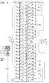
- FIG. 4 An analog-to-digital converter 200, incorporating a digital-to-analog converter in accordance with the illustrative embodiment of the invention, is shown in Figure 4.
- the analog-to-digital converter converts an analog current signal to a corresponding digitally encoded signal.
- Switching transistors M1 through M17 may be configured as disclosed above or in any known configuration.
- the analog-to-digital conversion is completed in a two step sequence. In the first step, the analog current is passed through the resistor string to generate a voltage. The voltage developed across the entire resistor string is held by a sample-and-hold circuit. In the second step, successive approximation circuitry generates a series of intermediate tap voltages with each iteration that more closely approximates the voltage maintained by the sample-and-hold circuit. The successive approximation process continues until the digital equivalent of the voltage held by the sample-and-hold circuit is determined.
- an analog current signal 202 is received on line 201 with transistors M30, M31, and M34 switched to be in the on state and transistors M32 and M33 switched to be in the off state.
- Transistor M34 being on dumps the current produced by current source 212 to ground.
- the voltage developed across resistor string 214 charges capacitor 203 and provides the positive input to comparator 204.
- Transistors M30, M31, and M34 are then switched to be in the off state and transistors M32 and M33 are switched to be in the on state.
- Transistor M33 being on dumps analog current signal 202 to ground.
- Transistors M30, M31, M32, M33, and M34 together with capacitor 203 comprise a sample-and-hold circuit that maintains the voltage developed across resistor sting 214 as the positive input to comparator 204.
- Successive approximation circuitry 206 initially turns on the appropriate switching transistor or transistors M1 through M17 to produce the midpoint voltage of resistor string 214 at output node 314.
- the voltage at output node 314 provides the negative input to comparator 204 where it is compared to the voltage maintained on capacitor 203.
- the midpoint of the upper half of the resistor string 214 is electrically coupled as the input to comparator 204 and compared to the voltage maintained on capacitor 203. If the output 232 is negative, the midpoint of the lower half of the resistor string 214 is electrically coupled as the input to comparator 204.
- the selection of the switching transistor or transistors that are switched on, as described above, are controlled by successive approximation circuitry 206. Starting with a default bit pattern, each iteration determines one bit in the binary, or other coded, representation 234, and the successive approximation process continues until all bits are determined.
- the successive approximation process is known to those skilled in the art and may be implemented as described above or in any known manner.
- the binary representation 234 is provided as the output of successive approximation circuitry 206 and analog-to-digital converter 200.
- the invention is particularly useful in communication systems and equipment employing integrated circuits in digital-to-analog and analog-to-digital converter applications.
- Such communication systems and equipment have the advantage of being more immune to noise induced in the resistor string of converters.
- analog-to-digital converter shown in Figure 4 is shown as operating in the single-ended mode, those skilled in the art could fabricate an analog-to-digital converter that operates in the differential mode.
Landscapes
- Engineering & Computer Science (AREA)
- Theoretical Computer Science (AREA)
- Analogue/Digital Conversion (AREA)
Abstract
There is disclosed an integrated circuit that includes a digital-to-analog converter (e.g., 10) having a resistor string (e.g., 14) driven by a current source (e.g., 12). The resistor string is coupled to the current source. Intermediate taps (e.g., T₁ through Tn+1) are defined at the resistor junctions as well the resistor-current source junctions. Switching transistors (e.g., M₁ through Mn+1) are coupled between an output node and a respective intermediate tap. A selection circuit (e.g., 2) is coupled to a terminal of each switching transistor for selectively switching the transistors to a predetermined state to electrically couple the associated intermediate tap to the output node (e.g., 16).
Description
- This invention relates generally to digital-to-analog converters (DACs), and more particularly to such converters driven by a current source.
- DACs are used to convert a digitally coded signal to an analog signal, or in conjunction with successive approximation circuitry as part of an analog-to-digital converter. DACs may employ a voltage applied across a resistor string. Switches, such as transistors, couple intermediate taps at the resistor junctions, as well as at the resistor-potential junctions, to an output node. The digitally coded signal is decoded to determine which switch to turn on. The magnitude of an analog voltage produced at the output node depends on which switch is turned on. Precisely generating an analog voltage that corresponds to a digitally coded signal necessitates the resistors of the resistance string have identical resistances. Even with identical resistances in the resistor string, the analog voltage at the output node can be inaccurate because any noise voltage induced in series with the reference voltage source of a voltage driven resistor string DAC changes the voltage across each resistor in the resistor string, and thus the voltage at each intermediate tap. The noise voltage at each intermediate tap is not the same, resulting in an erroneous analog voltage being produced at the output node.
- In accordance with an illustrative embodiment of the present invention, an integrated circuit includes a digital-to-analog converter in which a resistor string is driven by a current source. Intermediate taps are defined at the resistor junctions as well the resistor-current source junctions. Switching transistors are coupled between an output node and respective intermediate taps. A selection circuit is coupled to a terminal of each switching transistor for selectively switching the transistors to a predetermined state to electrically couple the associated intermediate tap to the output node.
-
- Figure 1 is a schematic diagram of a single-ended mode digital-to-analog converter in accordance with an illustrative embodiment of the present invention;
- Figure 2 is a schematic diagram of a differential mode digital-to-analog converter in accordance with an illustrative embodiment of the invention;
- Figure 3 is a schematic diagram of a differential mode digital-to-analog converter capable of achieving an additional bit of precision; and
- Figure 4 is a schematic diagram of an analog-to-digital converter.
- The schematic diagram of a
DAC 10 in accordance with an illustrative embodiment of the present invention is shown in Figure 1.DAC 10 is shown operating in a single-ended mode.DAC 10 includes a current source coupled to a resistor string to provide a constant current to the resistor string. Switches, shown as MOS transistors, couple intermediate taps to a common output node. The magnitude of an analog voltage produced at the output node depends on which switch or switches are turned on. The output may be amplified by an output amplifier. A DAC in accordance with the present invention is suitable for fabrication in the form of a monolithic integrated circuit. -
Resistor string 14 is comprised of a user-determined number, n, of resistors in series, denoted R₁ through Rn. The resistor string is coupled to acurrent source 12 which, whenDAC 10 is employed as a digital-to-analog converter, provides a known constant current toresistor string 14. The resistance values of the resistors comprising the resistor string are application dependent and can be readily selected by one skilled in the art based on a variety of parameters such as the power to be dissipated, the potential across the resistor string, and the number of resistors in the resistor string. At the resistor junctions, as well as at the current source-resistor junctions, a switch is coupled between the junction andoutput node 16. The junctions define intermediate taps T₁ through Tn+1. The switches, preferably transistors, are shown in the illustrative embodiment as MOS transistors M₁ through Mn+1. - Transistor M₁ is coupled between the junction of the positive terminal of
current source 12 and resistor R₁, andoutput node 16. Transistor Mn+1 is coupled between the junction of the negative terminal ofcurrent source 12 and resistor Rn, andoutput node 16. Transistors M₂ through Mn each couple an intermediate tap, T₂ through Tn respectively, withoutput node 16. The transistors are typically identical and have an impedance in the conductive state that is very large compared to the resistance of resistors inresistor string 14.Output amplifier 18 amplifies the output signal atoutput node 16 and may convert the output to another form, such as from a voltage output to a current output. - As is known in the digital-to-analog converter art, a digitally encoded signal 6, representative of the desired analog signal, is provided to a decode circuit. The decode circuit decodes the digitally encoded signal and a driver circuit turns on the appropriate switch or switches to conduct the voltage at the associated intermediate tap(s) to the output node. A single switch may be turned on, or multiple switches may be switched to be in the on state simultaneously. Switching transistors M₁ through Mn+1 are controlled by switching transistor selection and
driver circuit 2. A monotonic input-output characteristic, providing a staircase output voltage atoutput node 16 for increasing digitally encoded inputs 6 is derived from the intermediate taps T₁ through Tn+1. - In accordance with the present invention,
current source 12 provides a constant current toresistor string 14. One or more of transistors M₁ through Mn+1 is switched on to couple respective ones of the intermediate taps tooutput node 16. By selectively switching on transistors M₁ through Mn+1, the voltage inresistor string 14 at the associated intermediate tap is provided atoutput node 16. Voltages intermediate the voltages at the intermediate taps may be provided atoutput node 16 by selectively switching on multiple ones of transistors M₁ through Mn+1. - Any noise voltage, induced in the current source-resistor string loop does not alter the current because of the high impedance inherent in
current source 12. Since the voltage produced atoutput node 16 depends only on the current passing throughresistor string 14 and the resistance of the resistors inresistor string 14, the accuracy of the voltage produced atoutput node 16 is immune to such a noise voltage. - The current driven DAC can also be operated in a differential mode. A
differential mode DAC 100 is illustrated in the schematic diagram of Figure 2.Resistor string 114 illustratively has twenty four resistors, thereby defining twenty five intermediate taps, T₁ through T₂₅. The middle intermediate tap is coupled to a reference potential, such as ground. Absent noise and with a constant current provided bycurrent source 112, intermediate taps T₁ through T₁₂ operate at a positive voltage, intermediate tap T₁₃ is maintained at ground potential, and intermediate taps T₁₄ through T₂₅ operate at a negative voltage. To provide an analog output voltage atoutput 118, switching transistors are turned on symmetrically about the intermediate tap coupled to a reference voltage. Whereas withDAC 10, a single switching transistor may be turned on to provide an analog output voltage, withDAC 100 transistors are turned on in pairs symmetrically about the intermediate tap coupled to the reference voltage. For example, if transistor M₆ is turned on, transistor M₂₀ is also turned on. If transistors M₂ and M₃ are turned on to provide an analog output voltage atoutput 118, transistors M₂₄ and M₂₃ are also turned on. Multiple transistors on both the positive and negative voltage sides ofresistor string 114 ofdifferential mode DAC 100 can be turned on in accordance with the teaching of U.S. Patent Application Serial Number 08/327174 entitled "Digital-To-Analog Converter With Reduced Number Of Resistors And Method Of Using," filed concurrently herewith and hereby incorporated by reference. - Turning on one or more transistors M₁ through M₁₂ operating on the positive voltage side of
resistor string 14, charges capacitor C1. Similarly, turning on one or more transistors M₁₄ through M₂₅ operating on the negative voltage side ofresistor string 114 charges capacitor C2. When the charging of the capacitor is complete, the currents in the switches go to zero. Thus the voltage drops across each switch also go to zero. The DAC operation is not affected by the switch resistance or switch nonlinearity. It is thus important that the switches remain closed until the current decreases to zero for operation of the DAC. - The switching transistor on the positive voltage side of
resistor string 114 in conjunction with capacitor C1 form sample and holdcircuit 120. The switching transistors on the negative voltage side ofresistor string 114 in conjunction with capacitor C2 form sample and holdcircuit 122. The capacitor voltages provide the positive and negative inputs todifferential amplifier 124. The capacitor voltages are added bydifferential amplifier 124 to reject any common mode noise, resulting in a noise-immune analog output voltage atoutput 118 ofdifferential amplifier 124. - Figure 3 shows a schematic circuit of a
DAC 110 capable of converting a digitally encoded input having an additional bit to an analog output using the same number of resistors in the resistor string and number of switches coupled to the intermediate taps as in the embodiment shown in Figure 2.DAC 110 permits the digitally encoded signal to have one more bit thanDAC 100 and produces twice the number of discrete analog outputs, with the analog outputs extending over both a positive and negative range. Typically, the midpoint of the range of digitally encoded inputs corresponds to the zero analog output. Other techniques can also be used to convert the entire range of digitally encoded inputs to outputs. Two levels of decoding are employed. The least significant bits are decoded to produce the magnitude of the signal. The most significant bit is decoded in a second stage to determine which resistor signal is coupled to which capacitor. - An analog-to-
digital converter 200, incorporating a digital-to-analog converter in accordance with the illustrative embodiment of the invention, is shown in Figure 4. The analog-to-digital converter converts an analog current signal to a corresponding digitally encoded signal. Switching transistors M₁ through M₁₇ may be configured as disclosed above or in any known configuration. The analog-to-digital conversion is completed in a two step sequence. In the first step, the analog current is passed through the resistor string to generate a voltage. The voltage developed across the entire resistor string is held by a sample-and-hold circuit. In the second step, successive approximation circuitry generates a series of intermediate tap voltages with each iteration that more closely approximates the voltage maintained by the sample-and-hold circuit. The successive approximation process continues until the digital equivalent of the voltage held by the sample-and-hold circuit is determined. - In analog-to-
digital converter 200, an analogcurrent signal 202 is received online 201 with transistors M₃₀, M₃₁, and M₃₄ switched to be in the on state and transistors M₃₂ and M₃₃ switched to be in the off state. Transistor M₃₄ being on dumps the current produced bycurrent source 212 to ground. The voltage developed acrossresistor string 214charges capacitor 203 and provides the positive input tocomparator 204. Transistors M₃₀, M₃₁, and M₃₄ are then switched to be in the off state and transistors M₃₂ and M₃₃ are switched to be in the on state. Transistor M₃₃ being on dumps analogcurrent signal 202 to ground. Transistors M₃₀, M₃₁, M₃₂, M₃₃, and M₃₄ together withcapacitor 203 comprise a sample-and-hold circuit that maintains the voltage developed acrossresistor sting 214 as the positive input tocomparator 204.Successive approximation circuitry 206 initially turns on the appropriate switching transistor or transistors M₁ through M₁₇ to produce the midpoint voltage ofresistor string 214 atoutput node 314. The voltage atoutput node 314 provides the negative input tocomparator 204 where it is compared to the voltage maintained oncapacitor 203. Ifoutput 232 fromcomparator 204, representing the difference between the voltage maintained oncapacitor 203 and the voltage generated atoutput node 314 by the current successive approximation iteration is positive, the midpoint of the upper half of theresistor string 214 is electrically coupled as the input tocomparator 204 and compared to the voltage maintained oncapacitor 203. If theoutput 232 is negative, the midpoint of the lower half of theresistor string 214 is electrically coupled as the input tocomparator 204. The selection of the switching transistor or transistors that are switched on, as described above, are controlled bysuccessive approximation circuitry 206. Starting with a default bit pattern, each iteration determines one bit in the binary, or other coded,representation 234, and the successive approximation process continues until all bits are determined. The successive approximation process is known to those skilled in the art and may be implemented as described above or in any known manner. Thebinary representation 234 is provided as the output ofsuccessive approximation circuitry 206 and analog-to-digital converter 200. - The invention is particularly useful in communication systems and equipment employing integrated circuits in digital-to-analog and analog-to-digital converter applications. Such communication systems and equipment have the advantage of being more immune to noise induced in the resistor string of converters.
- While the analog-to-digital converter shown in Figure 4 is shown as operating in the single-ended mode, those skilled in the art could fabricate an analog-to-digital converter that operates in the differential mode.
Claims (10)
- An integrated circuit including a digital-to-analog converter for providing an analog output at an output node, the digital-to-analog converter including an energy source (e.g., 12, 112, 212) having a positive terminal and a negative terminal, a resistor string (e.g., 14, 114, 214) coupled across the positive and negative terminals of the energy source, the resistor string comprising a plurality of serially coupled resistors (e.g., R₁-Rn; R₁-R₂₄; R₁-R₁₆) and providing a current path, intermediate taps (e.g., T₁-Tn+1; T₁-T₂₅; T₁-T₁₇) defined at the junctions of resistors in the resistor string and at the junction of the resistor string and the positive and negative terminals of the energy source, a plurality of switching transistors, (e.g., M₁-Mn+1; M₁-M₂₅; M₁-M₁₇) each of the switching transistors coupled between the output node (e.g., 16, 18, 232) and a respective intermediate tap, and a selection circuit (e.g., 2, 206) coupled to a terminal of each switching transistor for selectively switching the transistors to a predetermined state, whereby an intermediate tap (e.g., T₁-Tn+1; T₁-T₂₅; T₁-T₁₇) is coupled to the output node (e.g., 16, 118, 232) when the corresponding switching transistor is switched to the predetermined state, the digital-to-analog converter characterized in that:
the energy source is a current source. - An integrated circuit as recited in claim 1, further characterized in that only one switching transistor (e.g., M₁-Mn+1; M₁-M₂₅; M₁-M₁₇) is capable of being switched to the predetermined state at a time.
- An integrated circuit as recited in claim 1, further characterized in that at least two switching transistors (e.g., M₁-Mn+1; M₁-M₂₅; M₁-M₁₇) are capable of being switched to be in the predetermined state simultaneously.
- An integrated circuit for providing an analog output, the integrated circuit including an energy source (e.g., 112, 212) having a positive terminal and a negative terminal, a resistor string (e.g., 114, 214) coupled across the positive and negative terminals of the energy source, the resistor string comprising a plurality of serially coupled resistors (e.g., R₁-R₂₄; R₁-R₁₆) and providing a current path, intermediate taps (e.g., T₁-T₂₅; T₁-T₁₇) defined at the junctions of resistors in the resistor string, and at the junction of the resistor string and the positive and negative terminals of the energy source, one of the intermediate taps (e.g., T₁₃) coupled to a reference potential, said one intermediate tap dividing the other intermediate taps into a first group of intermediate taps (e.g., T₁ through T₁₂) between said one intermediate tap and the positive terminal of the energy source and a second group of intermediate taps (e.g., T₁₄ through T₂₅) between said one intermediate tap (e.g., T₁₃) and the negative terminal of the energy source, a first plurality of switching transistors (e.g., M₁ through M₁₂), each of the first plurality of switching transistors coupled between a first node and a respective intermediate tap of the first group of intermediate taps, a second plurality of switching transistors (e.g., M₁₄ through M₂₅), each of the second plurality of switching transistors coupled between a second output node and a respective intermediate tap of the second group of intermediate taps, and a differential amplifier (e.g., 124) having first and second input ports and an output port, the first input port of the differential amplifier coupled to the first output node to receive a signal therefrom, the second input port of the differential amplifier coupled to the second output node to received a signal therefrom, the differential amplifier providing a signal at its output port (e.g., 118) that is the difference between the signals received at its first and second input ports, whereby common mode noise is rejected from an analog signal produced at the output of the differential amplifier, the integrated circuit characterized in that:
the energy source is a current source. - An integrated circuit as recited in claim 4, further characterized by a selection circuit (e.g., 2, 206) coupled to a terminal of each switching transistor in the first and second plurality of switching transistors, the selection circuit for switching the state of selected ones of the transistors to a predetermined state in response to a digitally encoded signal.
- An integrated circuit as recited in claim 4, further characterized in that the converter operates in a differential mode.
- An integrated circuit as recited in claim 4, further characterized in that the selection circuit (e.g., 2, 206) is capable of switching at least two switching transistors to be in the predetermined state simultaneously.
- An integrated circuit as recited in claim 7, further characterized in that one of said at least two switching transistors is in the first plurality of switching transistors (e.g., M₁ through M₁₂) and another of said at least two switching transistors is in the second plurality of switching transistors (e.g., M₁₄ through M₂₅).
- An integrated circuit including an analog-to-digital converter for generating a digital representation of an analog signal, the analog-to-digital converter including an energy source (e.g., 212) having a positive terminal and a negative terminal, a resistor string (e.g., 214) providing a current path, the resistor string comprising a plurality of serially coupled resistors (e.g., R₁-R₁₆), the resistor string coupled across the positive and negative terminals of the energy source, intermediate taps (e.g., T₁-T₁₇) defined at the junctions of resistors in the resistor string and at the junction of the resistor string and the positive and negative terminals of the energy source, a plurality of switching transistors (e.g., M₁-M₁₇), each of the switching transistors coupled between an output node (e.g., 314) and a respective intermediate tap, a comparator (e.g., 204) having first and second input leads and an output port (e.g., 232), the first input lead coupled to the output node (e.g., 324) to receive the generated analog signal, the second input lead coupled to receive the analog signal, the comparator providing a difference signal at its output port (e.g., 232) that is the difference between the signals received at its first and second input leads, and a successive approximation switching transistor selection and driving circuit (e.g., 206), the successive approximation circuit receiving the difference signal output from the comparator, the successive approximation circuit coupled to a terminal of each of the plurality of switching transistors for selectively switching the switching transistors to a predetermined state, to produce the generated analog signal when the resistor string is energized by an energy source, the successive approximation circuit successively approximating the analog signal and producing a digital representation thereof as an output, characterized in that:
the energy source is a current source. - An integrated circuit as recited in claim 1 or 9, further characterized in that the converter operates in a single-ended mode.
Applications Claiming Priority (2)
| Application Number | Priority Date | Filing Date | Title |
|---|---|---|---|
| US327162 | 1981-12-02 | ||
| US08/327,162 US5619203A (en) | 1994-10-21 | 1994-10-21 | Current source driven converter |
Publications (1)
| Publication Number | Publication Date |
|---|---|
| EP0708530A1 true EP0708530A1 (en) | 1996-04-24 |
Family
ID=23275428
Family Applications (1)
| Application Number | Title | Priority Date | Filing Date |
|---|---|---|---|
| EP95307418A Withdrawn EP0708530A1 (en) | 1994-10-21 | 1995-10-18 | Current source driven DA converter and AD using the same |
Country Status (6)
| Country | Link |
|---|---|
| US (1) | US5619203A (en) |
| EP (1) | EP0708530A1 (en) |
| JP (1) | JPH08213911A (en) |
| KR (1) | KR960016161A (en) |
| CN (1) | CN1131845A (en) |
| TW (1) | TW269075B (en) |
Cited By (1)
| Publication number | Priority date | Publication date | Assignee | Title |
|---|---|---|---|---|
| CN112088345A (en) * | 2018-05-09 | 2020-12-15 | 德州仪器公司 | Integrated circuit with a set of series-connected resistors |
Families Citing this family (24)
| Publication number | Priority date | Publication date | Assignee | Title |
|---|---|---|---|---|
| US5731775A (en) * | 1996-06-17 | 1998-03-24 | Lucent Technologies Inc. | Subranging converter with plurality of resistor strings and transistor switches |
| US5703588A (en) * | 1996-10-15 | 1997-12-30 | Atmel Corporation | Digital to analog converter with dual resistor string |
| US6008749A (en) * | 1997-12-22 | 1999-12-28 | Lucent Technologies, Inc. | Mask programmable low power voltage/current-mode ADC |
| JP3779056B2 (en) * | 1998-01-30 | 2006-05-24 | 富士通株式会社 | Voltage generation circuit and D / A conversion circuit |
| US6225929B1 (en) | 1998-12-02 | 2001-05-01 | Hewlett-Packard Company | Digital-to-analog converter having switchable current sources and resistor string |
| JP4742401B2 (en) * | 2000-03-31 | 2011-08-10 | ソニー株式会社 | Digital-analog conversion circuit and display device equipped with the same |
| US6268819B1 (en) * | 1999-06-29 | 2001-07-31 | Texas Instruments Corporated | Bit interpolation in a resistor string data converter |
| US6448917B1 (en) | 2000-05-31 | 2002-09-10 | Cygnal Integrated Products, Inc. | DAC using current source driving main resistor string |
| US6400300B1 (en) * | 2000-05-31 | 2002-06-04 | Cygnal Integrated Products, Inc. | D/A converter street effect compensation |
| US6433717B1 (en) | 2000-05-31 | 2002-08-13 | Cygnal Integrated Products, Inc. | D/A resistor strings with cross coupling switches |
| US6384763B1 (en) * | 2000-05-31 | 2002-05-07 | Cygnal Integrated Products, Inc. | Segemented D/A converter with enhanced dynamic range |
| JP4571297B2 (en) * | 2000-11-20 | 2010-10-27 | 旭化成エレクトロニクス株式会社 | D / A converter |
| JPWO2002080371A1 (en) * | 2001-03-29 | 2004-07-22 | 株式会社鷹山 | DA converter |
| JP2003029687A (en) * | 2001-07-16 | 2003-01-31 | Sony Corp | D/a conversion circuit, display device using the same circuit and portable terminal using the same device |
| US6954165B2 (en) * | 2003-03-28 | 2005-10-11 | Ess Technology, Inc. | Voltage segmented digital to analog converter |
| JP4016968B2 (en) * | 2004-05-24 | 2007-12-05 | セイコーエプソン株式会社 | DA converter, data line driving circuit, electro-optical device, driving method thereof, and electronic apparatus |
| KR101256001B1 (en) * | 2004-07-08 | 2013-04-18 | 오끼 덴끼 고오교 가부시끼가이샤 | Driving circuit of the liquid crystal display device |
| US7283079B2 (en) * | 2006-01-03 | 2007-10-16 | Analog Devices, Inc | Digital to analog converter having a single cyclic resistor string and multiple current sources |
| CN102291147A (en) * | 2011-05-31 | 2011-12-21 | 深圳市博驰信电子有限责任公司 | Analog-digital conversion circuit, analog-digital converter and analog-digital conversion method |
| US8884799B2 (en) * | 2013-03-15 | 2014-11-11 | Qualcomm Incroporated | Dual-string digital-to-analog converters (DACs), and related circuits, systems, and methods |
| US9397688B2 (en) * | 2014-09-10 | 2016-07-19 | Texas Instruments Incorporated | Hybrid digital-to-analog conversion system |
| CN106253898B (en) * | 2015-06-06 | 2021-09-03 | 硅实验室公司 | Apparatus for gain selection with parasitic element compensation and related methods |
| US10516408B2 (en) * | 2018-03-08 | 2019-12-24 | Analog Devices Global Unlimited Company | Analog to digital converter stage |
| US11418210B2 (en) * | 2020-05-05 | 2022-08-16 | Omni Design Technologies, Inc. | Digital-to-analog converter with reference voltage selection switch |
Citations (9)
| Publication number | Priority date | Publication date | Assignee | Title |
|---|---|---|---|---|
| US3997892A (en) * | 1973-07-27 | 1976-12-14 | Trw Inc. | Digital to analog converter with improved companding |
| US4198622A (en) * | 1978-02-21 | 1980-04-15 | National Semiconductor Corporation | Double digital-to-analog converter |
| EP0123222A2 (en) * | 1983-04-18 | 1984-10-31 | Kabushiki Kaisha Toshiba | Digital-to-analog converter |
| EP0152930A2 (en) * | 1984-02-17 | 1985-08-28 | Analog Devices, Inc. | Two-stage high-resolution digital-to-analog-converter |
| JPH01309518A (en) * | 1988-06-08 | 1989-12-13 | Fuji Electric Co Ltd | D/a converter |
| US4896157A (en) * | 1989-01-17 | 1990-01-23 | Motorola, Inc. | Digital to analog converter having single resistive string with shiftable voltage thereacross |
| US4973979A (en) * | 1987-12-21 | 1990-11-27 | Nissan Motor Company, Limited | Circuit and method for converting digital signal into corresponding analog signal |
| US4983974A (en) * | 1990-02-06 | 1991-01-08 | Motorola, Inc. | Analog-to-digital conversion by varying both inputs of a comparator utilizing successive approximation |
| US5243347A (en) * | 1992-09-28 | 1993-09-07 | Motorola, Inc. | Monotonic current/resistor digital-to-analog converter and method of operation |
Family Cites Families (22)
| Publication number | Priority date | Publication date | Assignee | Title |
|---|---|---|---|---|
| US3611353A (en) * | 1969-03-26 | 1971-10-05 | Beckman Instruments Inc | Digital-to-analog converter |
| US4034366A (en) * | 1976-01-28 | 1977-07-05 | Analog Devices, Inc. | Analog-to-digital converter with controlled ladder network |
| US4293848A (en) * | 1977-08-26 | 1981-10-06 | Intel Corporation | MOS Analog-to-digital converter |
| US4520461A (en) * | 1979-01-24 | 1985-05-28 | Xicor, Inc. | Integrated high voltage distribution and control systems |
| US4617652A (en) * | 1979-01-24 | 1986-10-14 | Xicor, Inc. | Integrated high voltage distribution and control systems |
| US4292625A (en) * | 1979-07-12 | 1981-09-29 | Advanced Micro Devices, Inc. | Monolithic digital-to-analog converter |
| US4263664A (en) * | 1979-08-31 | 1981-04-21 | Xicor, Inc. | Nonvolatile static random access memory system |
| JPS56153832A (en) * | 1980-04-30 | 1981-11-28 | Nec Corp | Digital to analog converter |
| US4281319A (en) * | 1980-06-30 | 1981-07-28 | Ricoh Company, Ltd. | Digital-to-analog converter |
| US4904922B1 (en) * | 1985-03-21 | 1992-09-01 | Apparatus for converting between digital and analog values | |
| US4668932A (en) * | 1985-07-26 | 1987-05-26 | Xicor, Inc. | Nonvolatile reprogrammable electronic potentiometer |
| JPH0761019B2 (en) * | 1986-06-19 | 1995-06-28 | 日本電気株式会社 | Analog to digital converter |
| US5014054A (en) * | 1987-07-22 | 1991-05-07 | Nippondenso Co., Ltd. | Digital-to-analog converter of the resistor string type |
| DE3813363A1 (en) * | 1988-04-21 | 1989-11-02 | Bayer Ag | MIXTURES OF THERMOPLASTIC POLYMERISATE IN POWDER FORM |
| US5036322A (en) * | 1989-06-02 | 1991-07-30 | Analog Devices, Inc. | Digital-to-analog converters with improved linearity |
| US5010337A (en) * | 1990-03-15 | 1991-04-23 | Analog Devices, Incorporated | High resolution D/A converter operable with single supply voltage |
| US5016014A (en) * | 1990-06-14 | 1991-05-14 | Ncr Corporation | High accuracy analog-to-digital converter with rail-to-rail reference and input voltage ranges |
| US5059978A (en) * | 1990-12-20 | 1991-10-22 | Vlsi Technology, Inc. | Resistor-string digital to analog converters with auxiliary coarse ladders |
| US5049882A (en) * | 1990-12-20 | 1991-09-17 | Burr-Brown Corporation | High speed analog-to-digital converter |
| JPH04329025A (en) * | 1991-04-30 | 1992-11-17 | Toshiba Corp | D/a converter |
| US5489904A (en) * | 1993-09-28 | 1996-02-06 | The Regents Of The University Of California | Analog current mode analog/digital converter |
| US5495245A (en) * | 1994-04-26 | 1996-02-27 | Analog Devices, Inc. | Digital-to-analog converter with segmented resistor string |
-
1994
- 1994-10-21 US US08/327,162 patent/US5619203A/en not_active Expired - Lifetime
- 1994-11-23 TW TW083110913A patent/TW269075B/en not_active IP Right Cessation
-
1995
- 1995-10-18 EP EP95307418A patent/EP0708530A1/en not_active Withdrawn
- 1995-10-20 CN CN95119912A patent/CN1131845A/en active Pending
- 1995-10-20 JP JP7271665A patent/JPH08213911A/en active Pending
- 1995-10-20 KR KR1019950036915A patent/KR960016161A/en not_active Application Discontinuation
Patent Citations (9)
| Publication number | Priority date | Publication date | Assignee | Title |
|---|---|---|---|---|
| US3997892A (en) * | 1973-07-27 | 1976-12-14 | Trw Inc. | Digital to analog converter with improved companding |
| US4198622A (en) * | 1978-02-21 | 1980-04-15 | National Semiconductor Corporation | Double digital-to-analog converter |
| EP0123222A2 (en) * | 1983-04-18 | 1984-10-31 | Kabushiki Kaisha Toshiba | Digital-to-analog converter |
| EP0152930A2 (en) * | 1984-02-17 | 1985-08-28 | Analog Devices, Inc. | Two-stage high-resolution digital-to-analog-converter |
| US4973979A (en) * | 1987-12-21 | 1990-11-27 | Nissan Motor Company, Limited | Circuit and method for converting digital signal into corresponding analog signal |
| JPH01309518A (en) * | 1988-06-08 | 1989-12-13 | Fuji Electric Co Ltd | D/a converter |
| US4896157A (en) * | 1989-01-17 | 1990-01-23 | Motorola, Inc. | Digital to analog converter having single resistive string with shiftable voltage thereacross |
| US4983974A (en) * | 1990-02-06 | 1991-01-08 | Motorola, Inc. | Analog-to-digital conversion by varying both inputs of a comparator utilizing successive approximation |
| US5243347A (en) * | 1992-09-28 | 1993-09-07 | Motorola, Inc. | Monotonic current/resistor digital-to-analog converter and method of operation |
Non-Patent Citations (1)
| Title |
|---|
| PATENT ABSTRACTS OF JAPAN vol. 014, no. 108 (E - 0896) 27 February 1990 (1990-02-27) * |
Cited By (2)
| Publication number | Priority date | Publication date | Assignee | Title |
|---|---|---|---|---|
| CN112088345A (en) * | 2018-05-09 | 2020-12-15 | 德州仪器公司 | Integrated circuit with a set of series-connected resistors |
| CN112088345B (en) * | 2018-05-09 | 2022-09-23 | 德州仪器公司 | Integrated circuit with a set of series-connected resistors |
Also Published As
| Publication number | Publication date |
|---|---|
| TW269075B (en) | 1996-01-21 |
| US5619203A (en) | 1997-04-08 |
| JPH08213911A (en) | 1996-08-20 |
| KR960016161A (en) | 1996-05-22 |
| CN1131845A (en) | 1996-09-25 |
Similar Documents
| Publication | Publication Date | Title |
|---|---|---|
| US5619203A (en) | Current source driven converter | |
| US5243347A (en) | Monotonic current/resistor digital-to-analog converter and method of operation | |
| US6686865B2 (en) | High resolution, high speed, low power switched capacitor analog to digital converter | |
| US4200863A (en) | Weighted capacitor analog/digital converting apparatus and method | |
| US6268817B1 (en) | Digital-to-analog converter | |
| US6621440B2 (en) | Digital to analogue converter | |
| US5059978A (en) | Resistor-string digital to analog converters with auxiliary coarse ladders | |
| US5604501A (en) | Digital-to-analog converter with reduced number of resistors | |
| US5283580A (en) | Current/resistor digital-to-analog converter having enhanced integral linearity and method of operation | |
| EP0153778A2 (en) | Multi-step parallel analog-digital converter | |
| JPH06152420A (en) | A/d converter | |
| US5633637A (en) | Digital-to-analog converter circuit | |
| US4812817A (en) | Differential analog-digital converter with switched capacitors | |
| US5748128A (en) | Reduced current quadratic digital/analog converter with improved settling-time | |
| US4306224A (en) | Analog-to-digital converting apparatus | |
| EP0558243A2 (en) | Digital to analog converter with precise linear output for both positive and negative digital input values | |
| EP0508454B1 (en) | A/D converter | |
| US20030011497A1 (en) | Data converter with background auto-zeroing via active interpolation | |
| US6856265B2 (en) | Data converter with background auto-zeroing via active interpolation | |
| EP0952672A2 (en) | Digital-to-analog conversion circuit and analog-to-digital conversion device using the circuit | |
| US6278393B1 (en) | Multiple output digital-to-analog converter | |
| JPS60216630A (en) | Step generator | |
| US4864304A (en) | Analog voltage signal comparator circuit | |
| US5896100A (en) | Method and apparatus for analog-to-digital or digital-to-analog conversion | |
| US4336527A (en) | Digital-to-analog converter |
Legal Events
| Date | Code | Title | Description |
|---|---|---|---|
| PUAI | Public reference made under article 153(3) epc to a published international application that has entered the european phase |
Free format text: ORIGINAL CODE: 0009012 |
|
| AK | Designated contracting states |
Kind code of ref document: A1 Designated state(s): DE ES FR GB IT NL |
|
| 17P | Request for examination filed |
Effective date: 19961010 |
|
| 17Q | First examination report despatched |
Effective date: 20000211 |
|
| STAA | Information on the status of an ep patent application or granted ep patent |
Free format text: STATUS: THE APPLICATION IS DEEMED TO BE WITHDRAWN |
|
| 18D | Application deemed to be withdrawn |
Effective date: 20000622 |