EP0706178B1 - Optical information medium, method for producing the optical information medium, and unit for producing the optical information medium - Google Patents
Optical information medium, method for producing the optical information medium, and unit for producing the optical information medium Download PDFInfo
- Publication number
- EP0706178B1 EP0706178B1 EP19950115521 EP95115521A EP0706178B1 EP 0706178 B1 EP0706178 B1 EP 0706178B1 EP 19950115521 EP19950115521 EP 19950115521 EP 95115521 A EP95115521 A EP 95115521A EP 0706178 B1 EP0706178 B1 EP 0706178B1
- Authority
- EP
- European Patent Office
- Prior art keywords
- substrate
- information signal
- signal layer
- film
- photopolymer resin
- Prior art date
- Legal status (The legal status is an assumption and is not a legal conclusion. Google has not performed a legal analysis and makes no representation as to the accuracy of the status listed.)
- Expired - Lifetime
Links
Images


Classifications
-
- G—PHYSICS
- G11—INFORMATION STORAGE
- G11B—INFORMATION STORAGE BASED ON RELATIVE MOVEMENT BETWEEN RECORD CARRIER AND TRANSDUCER
- G11B7/00—Recording or reproducing by optical means, e.g. recording using a thermal beam of optical radiation by modifying optical properties or the physical structure, reproducing using an optical beam at lower power by sensing optical properties; Record carriers therefor
- G11B7/24—Record carriers characterised by shape, structure or physical properties, or by the selection of the material
- G11B7/241—Record carriers characterised by shape, structure or physical properties, or by the selection of the material characterised by the selection of the material
- G11B7/252—Record carriers characterised by shape, structure or physical properties, or by the selection of the material characterised by the selection of the material of layers other than recording layers
- G11B7/256—Record carriers characterised by shape, structure or physical properties, or by the selection of the material characterised by the selection of the material of layers other than recording layers of layers improving adhesion between layers
-
- G—PHYSICS
- G11—INFORMATION STORAGE
- G11B—INFORMATION STORAGE BASED ON RELATIVE MOVEMENT BETWEEN RECORD CARRIER AND TRANSDUCER
- G11B7/00—Recording or reproducing by optical means, e.g. recording using a thermal beam of optical radiation by modifying optical properties or the physical structure, reproducing using an optical beam at lower power by sensing optical properties; Record carriers therefor
- G11B7/24—Record carriers characterised by shape, structure or physical properties, or by the selection of the material
- G11B7/241—Record carriers characterised by shape, structure or physical properties, or by the selection of the material characterised by the selection of the material
- G11B7/252—Record carriers characterised by shape, structure or physical properties, or by the selection of the material characterised by the selection of the material of layers other than recording layers
- G11B7/258—Record carriers characterised by shape, structure or physical properties, or by the selection of the material characterised by the selection of the material of layers other than recording layers of reflective layers
- G11B7/2585—Record carriers characterised by shape, structure or physical properties, or by the selection of the material characterised by the selection of the material of layers other than recording layers of reflective layers based on aluminium
-
- B—PERFORMING OPERATIONS; TRANSPORTING
- B29—WORKING OF PLASTICS; WORKING OF SUBSTANCES IN A PLASTIC STATE IN GENERAL
- B29C—SHAPING OR JOINING OF PLASTICS; SHAPING OF MATERIAL IN A PLASTIC STATE, NOT OTHERWISE PROVIDED FOR; AFTER-TREATMENT OF THE SHAPED PRODUCTS, e.g. REPAIRING
- B29C65/00—Joining or sealing of preformed parts, e.g. welding of plastics materials; Apparatus therefor
- B29C65/02—Joining or sealing of preformed parts, e.g. welding of plastics materials; Apparatus therefor by heating, with or without pressure
- B29C65/14—Joining or sealing of preformed parts, e.g. welding of plastics materials; Apparatus therefor by heating, with or without pressure using wave energy, i.e. electromagnetic radiation, or particle radiation
- B29C65/1403—Joining or sealing of preformed parts, e.g. welding of plastics materials; Apparatus therefor by heating, with or without pressure using wave energy, i.e. electromagnetic radiation, or particle radiation characterised by the type of electromagnetic or particle radiation
- B29C65/1406—Ultraviolet [UV] radiation
-
- B—PERFORMING OPERATIONS; TRANSPORTING
- B29—WORKING OF PLASTICS; WORKING OF SUBSTANCES IN A PLASTIC STATE IN GENERAL
- B29C—SHAPING OR JOINING OF PLASTICS; SHAPING OF MATERIAL IN A PLASTIC STATE, NOT OTHERWISE PROVIDED FOR; AFTER-TREATMENT OF THE SHAPED PRODUCTS, e.g. REPAIRING
- B29C65/00—Joining or sealing of preformed parts, e.g. welding of plastics materials; Apparatus therefor
- B29C65/02—Joining or sealing of preformed parts, e.g. welding of plastics materials; Apparatus therefor by heating, with or without pressure
- B29C65/14—Joining or sealing of preformed parts, e.g. welding of plastics materials; Apparatus therefor by heating, with or without pressure using wave energy, i.e. electromagnetic radiation, or particle radiation
- B29C65/1429—Joining or sealing of preformed parts, e.g. welding of plastics materials; Apparatus therefor by heating, with or without pressure using wave energy, i.e. electromagnetic radiation, or particle radiation characterised by the way of heating the interface
- B29C65/1435—Joining or sealing of preformed parts, e.g. welding of plastics materials; Apparatus therefor by heating, with or without pressure using wave energy, i.e. electromagnetic radiation, or particle radiation characterised by the way of heating the interface at least passing through one of the parts to be joined, i.e. transmission welding
-
- B—PERFORMING OPERATIONS; TRANSPORTING
- B29—WORKING OF PLASTICS; WORKING OF SUBSTANCES IN A PLASTIC STATE IN GENERAL
- B29C—SHAPING OR JOINING OF PLASTICS; SHAPING OF MATERIAL IN A PLASTIC STATE, NOT OTHERWISE PROVIDED FOR; AFTER-TREATMENT OF THE SHAPED PRODUCTS, e.g. REPAIRING
- B29C65/00—Joining or sealing of preformed parts, e.g. welding of plastics materials; Apparatus therefor
- B29C65/02—Joining or sealing of preformed parts, e.g. welding of plastics materials; Apparatus therefor by heating, with or without pressure
- B29C65/14—Joining or sealing of preformed parts, e.g. welding of plastics materials; Apparatus therefor by heating, with or without pressure using wave energy, i.e. electromagnetic radiation, or particle radiation
- B29C65/1477—Joining or sealing of preformed parts, e.g. welding of plastics materials; Apparatus therefor by heating, with or without pressure using wave energy, i.e. electromagnetic radiation, or particle radiation making use of an absorber or impact modifier
- B29C65/1483—Joining or sealing of preformed parts, e.g. welding of plastics materials; Apparatus therefor by heating, with or without pressure using wave energy, i.e. electromagnetic radiation, or particle radiation making use of an absorber or impact modifier coated on the article
-
- B—PERFORMING OPERATIONS; TRANSPORTING
- B29—WORKING OF PLASTICS; WORKING OF SUBSTANCES IN A PLASTIC STATE IN GENERAL
- B29C—SHAPING OR JOINING OF PLASTICS; SHAPING OF MATERIAL IN A PLASTIC STATE, NOT OTHERWISE PROVIDED FOR; AFTER-TREATMENT OF THE SHAPED PRODUCTS, e.g. REPAIRING
- B29C65/00—Joining or sealing of preformed parts, e.g. welding of plastics materials; Apparatus therefor
- B29C65/48—Joining or sealing of preformed parts, e.g. welding of plastics materials; Apparatus therefor using adhesives, i.e. using supplementary joining material; solvent bonding
- B29C65/4805—Joining or sealing of preformed parts, e.g. welding of plastics materials; Apparatus therefor using adhesives, i.e. using supplementary joining material; solvent bonding characterised by the type of adhesives
- B29C65/483—Reactive adhesives, e.g. chemically curing adhesives
- B29C65/4845—Radiation curing adhesives, e.g. UV light curing adhesives
-
- B—PERFORMING OPERATIONS; TRANSPORTING
- B29—WORKING OF PLASTICS; WORKING OF SUBSTANCES IN A PLASTIC STATE IN GENERAL
- B29C—SHAPING OR JOINING OF PLASTICS; SHAPING OF MATERIAL IN A PLASTIC STATE, NOT OTHERWISE PROVIDED FOR; AFTER-TREATMENT OF THE SHAPED PRODUCTS, e.g. REPAIRING
- B29C65/00—Joining or sealing of preformed parts, e.g. welding of plastics materials; Apparatus therefor
- B29C65/48—Joining or sealing of preformed parts, e.g. welding of plastics materials; Apparatus therefor using adhesives, i.e. using supplementary joining material; solvent bonding
- B29C65/52—Joining or sealing of preformed parts, e.g. welding of plastics materials; Apparatus therefor using adhesives, i.e. using supplementary joining material; solvent bonding characterised by the way of applying the adhesive
- B29C65/521—Joining or sealing of preformed parts, e.g. welding of plastics materials; Apparatus therefor using adhesives, i.e. using supplementary joining material; solvent bonding characterised by the way of applying the adhesive by spin coating
-
- B—PERFORMING OPERATIONS; TRANSPORTING
- B29—WORKING OF PLASTICS; WORKING OF SUBSTANCES IN A PLASTIC STATE IN GENERAL
- B29C—SHAPING OR JOINING OF PLASTICS; SHAPING OF MATERIAL IN A PLASTIC STATE, NOT OTHERWISE PROVIDED FOR; AFTER-TREATMENT OF THE SHAPED PRODUCTS, e.g. REPAIRING
- B29C66/00—General aspects of processes or apparatus for joining preformed parts
- B29C66/01—General aspects dealing with the joint area or with the area to be joined
- B29C66/05—Particular design of joint configurations
- B29C66/10—Particular design of joint configurations particular design of the joint cross-sections
- B29C66/11—Joint cross-sections comprising a single joint-segment, i.e. one of the parts to be joined comprising a single joint-segment in the joint cross-section
- B29C66/112—Single lapped joints
- B29C66/1122—Single lap to lap joints, i.e. overlap joints
-
- B—PERFORMING OPERATIONS; TRANSPORTING
- B29—WORKING OF PLASTICS; WORKING OF SUBSTANCES IN A PLASTIC STATE IN GENERAL
- B29C—SHAPING OR JOINING OF PLASTICS; SHAPING OF MATERIAL IN A PLASTIC STATE, NOT OTHERWISE PROVIDED FOR; AFTER-TREATMENT OF THE SHAPED PRODUCTS, e.g. REPAIRING
- B29C66/00—General aspects of processes or apparatus for joining preformed parts
- B29C66/40—General aspects of joining substantially flat articles, e.g. plates, sheets or web-like materials; Making flat seams in tubular or hollow articles; Joining single elements to substantially flat surfaces
- B29C66/41—Joining substantially flat articles ; Making flat seams in tubular or hollow articles
- B29C66/45—Joining of substantially the whole surface of the articles
- B29C66/452—Joining of substantially the whole surface of the articles the article having a disc form, e.g. making CDs or DVDs
-
- B—PERFORMING OPERATIONS; TRANSPORTING
- B29—WORKING OF PLASTICS; WORKING OF SUBSTANCES IN A PLASTIC STATE IN GENERAL
- B29C—SHAPING OR JOINING OF PLASTICS; SHAPING OF MATERIAL IN A PLASTIC STATE, NOT OTHERWISE PROVIDED FOR; AFTER-TREATMENT OF THE SHAPED PRODUCTS, e.g. REPAIRING
- B29C66/00—General aspects of processes or apparatus for joining preformed parts
- B29C66/70—General aspects of processes or apparatus for joining preformed parts characterised by the composition, physical properties or the structure of the material of the parts to be joined; Joining with non-plastics material
- B29C66/72—General aspects of processes or apparatus for joining preformed parts characterised by the composition, physical properties or the structure of the material of the parts to be joined; Joining with non-plastics material characterised by the structure of the material of the parts to be joined
- B29C66/723—General aspects of processes or apparatus for joining preformed parts characterised by the composition, physical properties or the structure of the material of the parts to be joined; Joining with non-plastics material characterised by the structure of the material of the parts to be joined being multi-layered
- B29C66/7232—General aspects of processes or apparatus for joining preformed parts characterised by the composition, physical properties or the structure of the material of the parts to be joined; Joining with non-plastics material characterised by the structure of the material of the parts to be joined being multi-layered comprising a non-plastics layer
- B29C66/72321—General aspects of processes or apparatus for joining preformed parts characterised by the composition, physical properties or the structure of the material of the parts to be joined; Joining with non-plastics material characterised by the structure of the material of the parts to be joined being multi-layered comprising a non-plastics layer consisting of metals or their alloys
-
- B—PERFORMING OPERATIONS; TRANSPORTING
- B32—LAYERED PRODUCTS
- B32B—LAYERED PRODUCTS, i.e. PRODUCTS BUILT-UP OF STRATA OF FLAT OR NON-FLAT, e.g. CELLULAR OR HONEYCOMB, FORM
- B32B37/00—Methods or apparatus for laminating, e.g. by curing or by ultrasonic bonding
- B32B37/12—Methods or apparatus for laminating, e.g. by curing or by ultrasonic bonding characterised by using adhesives
-
- G—PHYSICS
- G11—INFORMATION STORAGE
- G11B—INFORMATION STORAGE BASED ON RELATIVE MOVEMENT BETWEEN RECORD CARRIER AND TRANSDUCER
- G11B7/00—Recording or reproducing by optical means, e.g. recording using a thermal beam of optical radiation by modifying optical properties or the physical structure, reproducing using an optical beam at lower power by sensing optical properties; Record carriers therefor
- G11B7/24—Record carriers characterised by shape, structure or physical properties, or by the selection of the material
- G11B7/26—Apparatus or processes specially adapted for the manufacture of record carriers
-
- B—PERFORMING OPERATIONS; TRANSPORTING
- B29—WORKING OF PLASTICS; WORKING OF SUBSTANCES IN A PLASTIC STATE IN GENERAL
- B29C—SHAPING OR JOINING OF PLASTICS; SHAPING OF MATERIAL IN A PLASTIC STATE, NOT OTHERWISE PROVIDED FOR; AFTER-TREATMENT OF THE SHAPED PRODUCTS, e.g. REPAIRING
- B29C65/00—Joining or sealing of preformed parts, e.g. welding of plastics materials; Apparatus therefor
- B29C65/48—Joining or sealing of preformed parts, e.g. welding of plastics materials; Apparatus therefor using adhesives, i.e. using supplementary joining material; solvent bonding
- B29C65/4805—Joining or sealing of preformed parts, e.g. welding of plastics materials; Apparatus therefor using adhesives, i.e. using supplementary joining material; solvent bonding characterised by the type of adhesives
- B29C65/481—Non-reactive adhesives, e.g. physically hardening adhesives
- B29C65/4815—Hot melt adhesives, e.g. thermoplastic adhesives
-
- B—PERFORMING OPERATIONS; TRANSPORTING
- B29—WORKING OF PLASTICS; WORKING OF SUBSTANCES IN A PLASTIC STATE IN GENERAL
- B29C—SHAPING OR JOINING OF PLASTICS; SHAPING OF MATERIAL IN A PLASTIC STATE, NOT OTHERWISE PROVIDED FOR; AFTER-TREATMENT OF THE SHAPED PRODUCTS, e.g. REPAIRING
- B29C66/00—General aspects of processes or apparatus for joining preformed parts
- B29C66/70—General aspects of processes or apparatus for joining preformed parts characterised by the composition, physical properties or the structure of the material of the parts to be joined; Joining with non-plastics material
- B29C66/71—General aspects of processes or apparatus for joining preformed parts characterised by the composition, physical properties or the structure of the material of the parts to be joined; Joining with non-plastics material characterised by the composition of the plastics material of the parts to be joined
-
- B—PERFORMING OPERATIONS; TRANSPORTING
- B29—WORKING OF PLASTICS; WORKING OF SUBSTANCES IN A PLASTIC STATE IN GENERAL
- B29L—INDEXING SCHEME ASSOCIATED WITH SUBCLASS B29C, RELATING TO PARTICULAR ARTICLES
- B29L2017/00—Carriers for sound or information
- B29L2017/001—Carriers of records containing fine grooves or impressions, e.g. disc records for needle playback, cylinder records
- B29L2017/003—Records or discs
- B29L2017/005—CD''s, DVD''s
-
- B—PERFORMING OPERATIONS; TRANSPORTING
- B32—LAYERED PRODUCTS
- B32B—LAYERED PRODUCTS, i.e. PRODUCTS BUILT-UP OF STRATA OF FLAT OR NON-FLAT, e.g. CELLULAR OR HONEYCOMB, FORM
- B32B2310/00—Treatment by energy or chemical effects
- B32B2310/08—Treatment by energy or chemical effects by wave energy or particle radiation
- B32B2310/0806—Treatment by energy or chemical effects by wave energy or particle radiation using electromagnetic radiation
- B32B2310/0831—Treatment by energy or chemical effects by wave energy or particle radiation using electromagnetic radiation using UV radiation
-
- B—PERFORMING OPERATIONS; TRANSPORTING
- B32—LAYERED PRODUCTS
- B32B—LAYERED PRODUCTS, i.e. PRODUCTS BUILT-UP OF STRATA OF FLAT OR NON-FLAT, e.g. CELLULAR OR HONEYCOMB, FORM
- B32B2429/00—Carriers for sound or information
- B32B2429/02—Records or discs
-
- G—PHYSICS
- G11—INFORMATION STORAGE
- G11B—INFORMATION STORAGE BASED ON RELATIVE MOVEMENT BETWEEN RECORD CARRIER AND TRANSDUCER
- G11B7/00—Recording or reproducing by optical means, e.g. recording using a thermal beam of optical radiation by modifying optical properties or the physical structure, reproducing using an optical beam at lower power by sensing optical properties; Record carriers therefor
- G11B7/24—Record carriers characterised by shape, structure or physical properties, or by the selection of the material
- G11B7/241—Record carriers characterised by shape, structure or physical properties, or by the selection of the material characterised by the selection of the material
- G11B7/252—Record carriers characterised by shape, structure or physical properties, or by the selection of the material characterised by the selection of the material of layers other than recording layers
- G11B7/257—Record carriers characterised by shape, structure or physical properties, or by the selection of the material characterised by the selection of the material of layers other than recording layers of layers having properties involved in recording or reproduction, e.g. optical interference layers or sensitising layers or dielectric layers, which are protecting the recording layers
- G11B2007/25705—Record carriers characterised by shape, structure or physical properties, or by the selection of the material characterised by the selection of the material of layers other than recording layers of layers having properties involved in recording or reproduction, e.g. optical interference layers or sensitising layers or dielectric layers, which are protecting the recording layers consisting essentially of inorganic materials
- G11B2007/25706—Record carriers characterised by shape, structure or physical properties, or by the selection of the material characterised by the selection of the material of layers other than recording layers of layers having properties involved in recording or reproduction, e.g. optical interference layers or sensitising layers or dielectric layers, which are protecting the recording layers consisting essentially of inorganic materials containing transition metal elements (Zn, Fe, Co, Ni, Pt)
-
- G—PHYSICS
- G11—INFORMATION STORAGE
- G11B—INFORMATION STORAGE BASED ON RELATIVE MOVEMENT BETWEEN RECORD CARRIER AND TRANSDUCER
- G11B7/00—Recording or reproducing by optical means, e.g. recording using a thermal beam of optical radiation by modifying optical properties or the physical structure, reproducing using an optical beam at lower power by sensing optical properties; Record carriers therefor
- G11B7/24—Record carriers characterised by shape, structure or physical properties, or by the selection of the material
- G11B7/241—Record carriers characterised by shape, structure or physical properties, or by the selection of the material characterised by the selection of the material
- G11B7/252—Record carriers characterised by shape, structure or physical properties, or by the selection of the material characterised by the selection of the material of layers other than recording layers
- G11B7/257—Record carriers characterised by shape, structure or physical properties, or by the selection of the material characterised by the selection of the material of layers other than recording layers of layers having properties involved in recording or reproduction, e.g. optical interference layers or sensitising layers or dielectric layers, which are protecting the recording layers
- G11B2007/25705—Record carriers characterised by shape, structure or physical properties, or by the selection of the material characterised by the selection of the material of layers other than recording layers of layers having properties involved in recording or reproduction, e.g. optical interference layers or sensitising layers or dielectric layers, which are protecting the recording layers consisting essentially of inorganic materials
- G11B2007/25708—Record carriers characterised by shape, structure or physical properties, or by the selection of the material characterised by the selection of the material of layers other than recording layers of layers having properties involved in recording or reproduction, e.g. optical interference layers or sensitising layers or dielectric layers, which are protecting the recording layers consisting essentially of inorganic materials containing group 13 elements (B, Al, Ga)
-
- G—PHYSICS
- G11—INFORMATION STORAGE
- G11B—INFORMATION STORAGE BASED ON RELATIVE MOVEMENT BETWEEN RECORD CARRIER AND TRANSDUCER
- G11B7/00—Recording or reproducing by optical means, e.g. recording using a thermal beam of optical radiation by modifying optical properties or the physical structure, reproducing using an optical beam at lower power by sensing optical properties; Record carriers therefor
- G11B7/24—Record carriers characterised by shape, structure or physical properties, or by the selection of the material
- G11B7/241—Record carriers characterised by shape, structure or physical properties, or by the selection of the material characterised by the selection of the material
- G11B7/252—Record carriers characterised by shape, structure or physical properties, or by the selection of the material characterised by the selection of the material of layers other than recording layers
- G11B7/257—Record carriers characterised by shape, structure or physical properties, or by the selection of the material characterised by the selection of the material of layers other than recording layers of layers having properties involved in recording or reproduction, e.g. optical interference layers or sensitising layers or dielectric layers, which are protecting the recording layers
- G11B2007/25705—Record carriers characterised by shape, structure or physical properties, or by the selection of the material characterised by the selection of the material of layers other than recording layers of layers having properties involved in recording or reproduction, e.g. optical interference layers or sensitising layers or dielectric layers, which are protecting the recording layers consisting essentially of inorganic materials
- G11B2007/25716—Record carriers characterised by shape, structure or physical properties, or by the selection of the material characterised by the selection of the material of layers other than recording layers of layers having properties involved in recording or reproduction, e.g. optical interference layers or sensitising layers or dielectric layers, which are protecting the recording layers consisting essentially of inorganic materials containing sulfur
-
- G—PHYSICS
- G11—INFORMATION STORAGE
- G11B—INFORMATION STORAGE BASED ON RELATIVE MOVEMENT BETWEEN RECORD CARRIER AND TRANSDUCER
- G11B7/00—Recording or reproducing by optical means, e.g. recording using a thermal beam of optical radiation by modifying optical properties or the physical structure, reproducing using an optical beam at lower power by sensing optical properties; Record carriers therefor
- G11B7/24—Record carriers characterised by shape, structure or physical properties, or by the selection of the material
- G11B7/241—Record carriers characterised by shape, structure or physical properties, or by the selection of the material characterised by the selection of the material
- G11B7/252—Record carriers characterised by shape, structure or physical properties, or by the selection of the material characterised by the selection of the material of layers other than recording layers
- G11B7/253—Record carriers characterised by shape, structure or physical properties, or by the selection of the material characterised by the selection of the material of layers other than recording layers of substrates
- G11B7/2533—Record carriers characterised by shape, structure or physical properties, or by the selection of the material characterised by the selection of the material of layers other than recording layers of substrates comprising resins
- G11B7/2534—Record carriers characterised by shape, structure or physical properties, or by the selection of the material characterised by the selection of the material of layers other than recording layers of substrates comprising resins polycarbonates [PC]
-
- Y—GENERAL TAGGING OF NEW TECHNOLOGICAL DEVELOPMENTS; GENERAL TAGGING OF CROSS-SECTIONAL TECHNOLOGIES SPANNING OVER SEVERAL SECTIONS OF THE IPC; TECHNICAL SUBJECTS COVERED BY FORMER USPC CROSS-REFERENCE ART COLLECTIONS [XRACs] AND DIGESTS
- Y10—TECHNICAL SUBJECTS COVERED BY FORMER USPC
- Y10S—TECHNICAL SUBJECTS COVERED BY FORMER USPC CROSS-REFERENCE ART COLLECTIONS [XRACs] AND DIGESTS
- Y10S428/00—Stock material or miscellaneous articles
- Y10S428/913—Material designed to be responsive to temperature, light, moisture
-
- Y—GENERAL TAGGING OF NEW TECHNOLOGICAL DEVELOPMENTS; GENERAL TAGGING OF CROSS-SECTIONAL TECHNOLOGIES SPANNING OVER SEVERAL SECTIONS OF THE IPC; TECHNICAL SUBJECTS COVERED BY FORMER USPC CROSS-REFERENCE ART COLLECTIONS [XRACs] AND DIGESTS
- Y10—TECHNICAL SUBJECTS COVERED BY FORMER USPC
- Y10S—TECHNICAL SUBJECTS COVERED BY FORMER USPC CROSS-REFERENCE ART COLLECTIONS [XRACs] AND DIGESTS
- Y10S430/00—Radiation imagery chemistry: process, composition, or product thereof
- Y10S430/146—Laser beam
-
- Y—GENERAL TAGGING OF NEW TECHNOLOGICAL DEVELOPMENTS; GENERAL TAGGING OF CROSS-SECTIONAL TECHNOLOGIES SPANNING OVER SEVERAL SECTIONS OF THE IPC; TECHNICAL SUBJECTS COVERED BY FORMER USPC CROSS-REFERENCE ART COLLECTIONS [XRACs] AND DIGESTS
- Y10—TECHNICAL SUBJECTS COVERED BY FORMER USPC
- Y10T—TECHNICAL SUBJECTS COVERED BY FORMER US CLASSIFICATION
- Y10T428/00—Stock material or miscellaneous articles
- Y10T428/21—Circular sheet or circular blank
-
- Y—GENERAL TAGGING OF NEW TECHNOLOGICAL DEVELOPMENTS; GENERAL TAGGING OF CROSS-SECTIONAL TECHNOLOGIES SPANNING OVER SEVERAL SECTIONS OF THE IPC; TECHNICAL SUBJECTS COVERED BY FORMER USPC CROSS-REFERENCE ART COLLECTIONS [XRACs] AND DIGESTS
- Y10—TECHNICAL SUBJECTS COVERED BY FORMER USPC
- Y10T—TECHNICAL SUBJECTS COVERED BY FORMER US CLASSIFICATION
- Y10T428/00—Stock material or miscellaneous articles
- Y10T428/31504—Composite [nonstructural laminate]
- Y10T428/31678—Of metal
Description
- The present invention relates to an optical information medium formed by bonding two optical information substrates with each other; a method for producing the same; and a unit for producing the same. The present invention also relates to an optical information medium having two information signal layers for recording/reproducing information thereon/therefrom by irradiating and focusing a laser beam thereon; a method for producing the same; and a unit for producing the same.
- Recently, various optical information media such as an optical card and an optical disk have been practically used. A compact disk (hereinafter, simply referred to as a "CD"), in particular, has become remarkably popular. The video and audio information recorded as digital signals on a CD-ROM can now be processed easily by a computer. As a result, the value and the utility of a CD have been considerably increased in the information industry.
- In order to record/reproduce high-density information onto/from an optical disk, it is necessary to shorten the wavelength of the laser beam to be used for the recording and the reproduction and increase the numerical aperture (NA) of an objective lens. Thanks to the remarkable development in the technologies for producing semiconductor laser devices, video compression technologies and various kinds of peripheral technologies, it is currently possible to record video and audio information on one side of a disk with a diameter of 120 mm for a long time. For example, by using an objective lens with an NA of 0.6 and a red semiconductor laser with a wavelength of 650 nm, it is possible to reproduce information from the signal pits with a track pitch of 0.74 µm and a pit length as short as 0.40 µm in a highly reliable manner. If an 8-15 system is used as a modulation system, then one bit length becomes 0.25 µm. Therefore, it is possible to accomplish a density higher than that of a CD by 5 times or more. By setting the redundancy to be about 15%, information having a capacity of about 5 Gigabytes can be recorded on a disk with a diameter of 120 mm, and video and audio signals in compliance with
MPEG 2 standard can be recorded at 4.7 Mbps on average on one side of a disk with an equal size to that of a CD for about 142 minutes. - However, the allowable disk tilt of an objective lens with an increased NA is very small. For example, if a substrate with a thickness equal to that of a CD, i.e., 1.2 mm, is used, then the tilt allowable for an objective lens with an NA of 0.6 is about 0.25 degrees. The tilt is no larger than the error to be caused in installing an optical head onto a player. Therefore, if a tilt is caused by a deformation on the disk, then such a tilt is not allowable. Accordingly, it is difficult to practically use an objective lens with such a small tilt.
- By thinning the thickness of the substrate, such an objective lens with an increased NA can be used and a practical high-density optical disk can be accomplished. For example, by reducing the thickness of the substrate to one half of the thickness of a CD, i.e., 0.6 mm, the tilt allowable for an objective lens with an NA of 0.6 can be enlarged to about 0.75 degrees. As a result, even when an error of about 0.25 degrees is caused in installing an optical head, a tilt up to 0.5 degrees, actually caused by a deformation on a disk, is still allcwable.
- First, a method for producing a CD will be briefly described for comparison. By using a stamper on which an audio signal is recorded, a substrate, a side of which is used for recording the audio signal, is produced so as to be 1.2 mm thick by an injection molding method. Then, a reflective film made of aluminum or the like is formed on the audio signal recording surface by a sputtering method. Next, a photopolymer resin is applied on the reflective film and then irradiated with ultraviolet (UV) rays, thereby forming a protective film. A CD is produced in this way.
- If an optical disk with a single thin substrate is formed, then the disk is likely to be deformed by the weight thereof. In order to prevent such deformation, two substrates are bonded with each other. By attaching the two substrates, not only the mechanical strength of the disk can be increased but also the capacity of the disk is doubled, because the area usable for recording/reproducing the information thereon/therefrom can be doubled.
- A conventional method for producing such a disk formed by the bonding of two thin substrates will be described. First, by using a stamper on which information signals such as video signals and audio signals are recorded, a first thin substrate, a side of which is used for recording the information signals thereon, is produced by an injection molding method.
- Then, a reflective film made of aluminum or the like is formed on the information signal layer by a sputtering method. Next, a photopolymer resin is applied on the reflective film and then irradiated with UV rays, thereby forming a protective film. Furthermore, a second thin substrate is formed by using a second stamper on which different information signals are recorded, and then another reflective film and another protective film are formed in the same manner as the above.
- Thereafter, a hot-melt adhesive is applied onto the protective film of each of the two substrates by using a roll coater; the two substrates are bonded with each other so that the hot-melt adhesives applied on the surface of each of the protective films are bonded with each other; and then pressure is applied to the assembly, thereby forming a bonded disk obtained by assembling the first and the second substrates. This bonding method using a hot-melt adhesive is the same as the method used for producing a laser disk.
- The disk thus formed has a configuration in which the two substrates are integrated by opposing the protective films of the two substrates to each other and forming a hot-melt adhesive layer therebetween.
- The configuration of such a conventional bonded disk will be described with reference to Figure 8. As shown in Figure 8, an
information signal layer 102 is formed on one side of afirst substrate 101. Areflective film 103 made of a metallic material mainly composed of aluminum or the like is formed on theinformation signal layer 102, and aprotective film 104 is further formed thereon. On the other hand, aninformation signal layer 106 is formed on one side of asecond substrate 105. In the same way, areflective film 107 and aprotective film 108 are formed on theinformation signal layer 106. A hot-meltadhesive layer 109 is further provided between theprotective films first substrate 101 and thesecond substrate 105. - Document EP-A-0408763 discloses an improvement of such an optical disk, by first irradiating an UV ray curing resin provided on the outer and inner peripheries of the disk, and second, by heating the thermosetting resin provided between the two protective layers of the two reflective layers, so as to vertically place the substrates in the thermosetting process without deforming the substrates and without permitting the adhesive to flow.
- In order to realize an alternative optical information medium, a method in which two information signal layers for recording/reproducing information thereon/therefrom are formed by irradiating and focusing a laser beam from the same direction is disclosed in Japanese Laid-Open Patent Publication No. 3-209642 and USP No. 5,134,604. The reflectance of one of the information signal layers which is located closer to the laser beam incoming side is reduced, so that a sufficient amount of the laser beam can reach the other information signal layer distant from the laser beam incoming side and the information recorded on the respective information signal layers can be independently read out. Therefore, by using an optical information medium with the same size as that of a conventional medium, the area usable as the recording region can be doubled and the recording capacity can be considerably increased.
- With respect to such a conventional dual-layer disk, the operational principle of the disk where the two information signal layers are exclusively used for reproducing the information therefrom will be described. Figure 9 shows a case where the laser beam is focused on one of the two information signal layers which is distant from the laser beam incoming side. In Figure 9, an
information signal layer 152 is formed on one side of atransparent substrate 151 made of glass, resin, or the like. A semi-transparentthin film 153 is formed on theinformation signal layer 152 so as to partially reflect the laser beam. Anotherinformation signal layer 180 is formed over the semi-transparentthin film 153 via atransparent material 154. Since it is preferable for areflective film 181 formed on theinformation signal layer 180 to reflect substantially all of the incoming laser beam, thereflective film 181 is made of a metallic material such as aluminum. Aprotective film 182 made of photopolymer resin or the like is further formed on thereflective film 181. The laser beam focused and incident on theinformation signal layer 180 is denoted by 171. - In the case where the laser beam is focused on the
information signal layer 180, the information signals recorded on theinformation signal layer 180 can be reproduced, while the laser beam is partially reflected by theinformation signal layer 152 as denoted by 172 before the laser beam reaches theinformation signal layer 180. In such a case, if the thickness of thetransparent material 154 is sufficiently large, then the spot size of the laser beam on theinformation signal layer 152 becomes sufficiently large, so that the signals recorded on theinformation signal layer 152 cannot be reproduced, and the signals reproduced from theinformation signal layer 180 are not adversely affected by the signals recorded on theinformation signal layer 152. In addition, if the semi-transparentthin film 153 on theinformation signal layer 152 is formed so as to have a uniform thickness, then a local phase change is not generated in the incoming laser beam, and the diffraction phenomenon undesirable for reproducing a signal can be suppressed at a negligible level. On the other hand, in the case where the laser beam is focused on theinformation signal layer 152 closer to the laser beam incoming side, the laser beam is transmitted through the semi-transparentthin film 153. However, since the spot size of the laser beam on theinformation signal layer 180 becomes sufficiently large, the information signals recorded on theinformation signal layer 180 cannot be reproduced, and the signals reproduced from theinformation signal layer 152 are not adversely affected by the signals recorded on theinformation signal layer 180. - Figures 10A to 10C show a method for producing such a dual-layer optical information medium. The
transparent substrate 151 having theinformation signal layer 152 formed on one side thereof is formed by an injection molding method or the like in the same way as a CD substrate. As shown in Figure 10A, the semi-transparentthin film 153 is formed on theinformation signal layer 152 by a sputtering method or a vacuum evaporation method using atarget 161. Thetarget 161 is a material for composing the semi-transparentthin film 153 and is made of a metal such as Au and Al or a dielectric such as ZnS. Then, as shown in Figure 10B, aphotopolymer resin 154 to become thetransparent material 154 is inserted between astamper 162 for forming theinformation signal layer 180 and the semi-transparentthin film 153 formed on theinformation signal layer 152; pressure is applied to thestamper 162 so as to obtain a predetermined thickness of thetransparent material 154; and then UV rays 164 are irradiated through the semi-transparentthin film 153 and thetransparent material 154. - Next, as shown in Figure 10C, the
reflective film 181 is formed on theinformation signal layer 180 obtained by removing thestamper 162 by a sputtering method or a vacuum evaporation method using atarget 165. In the case where theinformation signal layer 180 is to be exclusively used for the reproduction, thetarget 165 is made of a metallic material such as aluminum. On the other hand, in the case where theinformation signal layer 180 is to be used for the recording and the reproduction, thetarget 165 is made of a phase-changeable material or a magneto-optical material. In performing this production method, thetransparent substrate 151 and the semi-transparentthin film 153 are required to transmit the UV rays. Finally, theprotective film 182 is formed on thereflective film 181 by using the photopolymer resin. - Since a conventional bonded disk is produced by a hot-melt method, the cost is considerably increased because an additional equipment such as a roll coater for applying a hot-melt adhesive and a presser is required in addition to the apparatus for producing a CD. On the other hand, since a new type of disk suitable for the use in a car is required to be developed from now on, such a disk is required to be resistant to the environment where the temperature reaches up to about 80°C and the humidity reaches up to about 85% for a long time. However, the hot-melt adhesive is softened at such a high temperature and high humidity, so that the disk is adversely deformed to exceed the allowable disk tilt.
- According to the conventional method for producing the dual-layer optical information medium, when the information signal layer distant from the laser beam incoming side is formed, a photopolymer resin is inserted between the stamper on which the information is recorded and the semi-transparent thin film formed on the information signal layer closer to the laser beam incoming side, and the UV rays are irradiated through the information signal layer closer to the laser beam incoming side while applying pressure to the resin. Accordingly, a process step for curing the resin with the UV rays and a process step for removing the resin from the stamper are required to be performed for producing each disk. In addition, a certain amount of time is required for removing the cured resin from the stamper and dust is likely to be attached to the resin, so that productivity is decreased, the cost necessary for producing the optical information medium becomes high and the optical information medium has many defects.
- The document DE-A-40 41 199 being reflected in the preambles of
claims 1, 14 and 17 describes a unit and a method for producing an optical information medium by fixing two discs to each other, for example by using a hot melt or, in the case that only one of the discs has a metal layer, a UV-resin, because this may then be cured through the semi-transparent layer replacing the metal layer. - The document DE-A-42 35 178 describes an optical recording disk also having two disc bases bonded to each other. The adhesive layer used for bonding contains a reaction initiator and the adhesive layer is hardened through polymerisation reaction by the reaction initiator and photopolymerisation reaction by ultraviolet ray irradiation.
- The optical information medium of the invention is defined in
present claim 1, and comprises: a first substrate having a first information signal layer; a first reflective film formed on the first information signal layer of the first substrate; a second substrate having a second information signal layer; a second reflective film formed on the second information signal layer of the second substrate; and a photopolymer resin film provided between the first reflective film and the second reflective film for bonding the first substrate (1) and the second substrate (5) with each other, the whole photopolymer resin film (60) being UV-cured. - In one embodiment of the invention, the first and the second reflective films are made of a metallic material mainly composed of aluminum.
- In another embodiment, at least one of the first and second reflective films has a thickness of 0,1 µm or less.
- In still another embodiment, the first and the second substrates have a substantially equal thickness.
- In still another embodiment, the first and the second substrate have a thickness of 0,57 mm to 0,63 mm.
- In still another embodiment, a pit art is formed on at least one of the first information signal layer and the second information signal layer.
- In still another embodiment, a recording material film is provided between the first substrate and the first reflective film and/or between the second substrate and the second reflective film.
- According to another aspect of the present invention, a method for producing an optical information medium, comprises the steps of: forming a first substrate having a first information signal layer on one side thereof; forming a first reflective film on the first information signal layer of the first substrate; forming a second substrate having a second information signal layer on one side thereof; forming a second reflective film on the second information signal layer of the second substrate; superposing the first and the second substrate so that the first and the second reflective films are opposed to each other with a photopolymer resin therebetween; and irradiating the whole photopolymer resin with light at least through the second substrate and the second reflective film so as to perform a multiple reflection of a part of the light between the first and the second reflective films and cure the photopolymer resin, thereby bonding the first and the second substrate with each other.
- In one embodiment, the photopolymer resin is a UV-curable photopolymer resin.
- In another embodiment, the step of superposing the first and second substrates comprises the steps of: applying the photopolymer resin in a donut shape while rotating the first substrate, and superposing the second substrate on the first substrate so that the first and the second reflective films are opposed to each other via the photopolymer resin so as to integrally rotate the first and the second substrates.
- In another embodiment, the method further comprises a step of disposing a transparent plate on the second substrate (5) so as to press the second substrate via the transparent plate (11) after performing the step of superposing the second substrate on the first substrate so as to integrally rotate the first and the second substrates.
- In still another embodiment, the first and the second reflective films are made of a metallic material mainly composed of aluminum.
- According to another aspect of the invention, a unit for producing such an optical information medium, as defined in present claim 14, by bonding the first substrate including the first reflective film formed on the first information signal layer of the first substrate, and the second substrate including the second reflective film formed on the second information signal layer of the second substrate with each other, comprises: an apparatus for applying the photopolymer resin on the first reflective film while rotating the first substrate; an apparatus for superposing the second substrate on the photopolymer resin so that the first and the second reflective films are opposed to each other; an apparatus for integrally rotating the first and the second substrates; and an apparatus for irradiating the photopolymer resin with light.
- In one embodiment, the unit further comprises an apparatus for pressing the second substrate via a transparent plate.
- In another aspect of the invention, a unit for producing such an optical information medium comprises: a first production block comprising a first molding machine for forming the first substrate including the first information signal layer thereon, and a first sputtering apparatus for forming the first reflective film on the first information signal layer of the first substrate; a second production block comprising a second molding machine for forming the second substrate including the second information signal layer thereon, and a second sputtering apparatus for forming the second reflective film on the second information signal layer of the second substrate; a third production block for opposing the first reflective film of the first substrate and the second reflective film of the second substrate via the photopolymer resin film with light at least through the second substrate and the second reflective film; and a transporter for moving the first substrate from the first production block to the third production block and moving the second substrate from the second production block to the third production block, respectively.
- According to still another aspect of the invention, An optical information medium is defined in present claim 17, and comprises: a first substrate having a first information signal layer; a semi-transparent film formed on the first information signal layer of the first substrate; a second substrate having a second information signal layer; a reflective film formed on the second information signal layer of the second substrate; and a photopolymer resin film provided between the semi-transparent film and the reflective film for bonding the first substrate and the second substrate with each other.
- In another embodiment, the reflective film includes a recording material film.
- In still another embodiment, a thickness of the first substrate is in a range of 0,55 to 0,61 mm.
- In still another embodiment, a thickness of the photopolymer resin is in a range of 30 to 60 µm.
- In still another embodiment, a pit art is formed on at least one of the first information signal layer and the second information signal layer.
- In still another aspect of the invention, a method for producing such an optical information medium is provided: the method comprises the steps of: forming a first substrate having a first information signal layer on one side thereof; forming a semi-transparent film on the first information signal layer of the first substrate; forming a second substrate having a second information signal layer on one side thereof; forming a reflective film on the second information signal layer of the second substrate; superposing the first and the second substrate so that the semi-transparent film and the reflective film are opposed to each other with a photopolymer resin therebetween; and irradiating the photopolymer resin with light at least through the first substrate and the semi-transparent film so as to perform a multiple reflection of a part of the light between the semi-transparent film and the reflective film, and cure the photopolymer resin, thereby bonding the first and the second substrates with each other.
- In another embodiment, the photopolymer resin is a UV-curable photopolymer resin.
- In another aspect of the invention, a unit for producing such an optical information medium comprises: a first production block comprising a first molding machine for forming a first substrate including a first information signal layer thereon, and a first sputtering apparatus for forming a semi-transparent film on the first information signal layer of the first substrate; a second production block comprising a second molding machine for forming a second substrate including a second information signal layer thereon, and a second sputtering apparatus for forming a reflective film on the second information signal layer of the second substrate; a third production block for opposing the semi-transparent film on the first substrate and the reflective film on the second substrate with each other, with a photopolymer resin film therebetween, and then irradiating the photopolymer resin film with light at least through the first substrate and the semi-transparent film; and a transporter for moving the first substrate from the first production block to the third production block and moving the second substrate from the second production block to the third production block, respectively.
- Thus, the invention described herein makes possible the advantage of providing an optical information medium which can be produced with a high yield and at a lower cost so as to have less defects, a method for producing the same and a unit for producing the same.
- This and other advantages of the present invention will become apparent to those skilled in the art upon reading and understanding the following detailed description with reference to the accompanying figures.
- Figure 1 is a cross-sectional view of an optical information medium according to a first example of the present invention.
- Figure 2 illustrates a UV ray irradiation process step in a method for producing an optical information medium of the present invention.
- Figures 3A to 3D are perspective views showing the respective process steps for producing the optical information medium according to the first example of the present invention.
- Figure 4 is a block diagram showing an arrangement for a unit for producing the optical information medium according to the first example of the present invention.
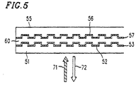
- Figure 5 is a cross-sectional view of an optical information medium according to a second example of the present invention.
- Figures 6A to 6C ore cross-sectional views showing the respective process steps for producing the optical information medium according to the second example of the present invention.
- Figure 7 is a block diagram showing an arrangement for a unit for producing the optical information medium according to the second example of the present invention.
- Figure 8 is a cross-sectional view of a conventional optical information medium.
- Figure 9 is a cross-sectional view of another conventional optical information medium.
- Figures 10A to 10C are cross-sectional views showing the respective process steps for producing a conventional optical information medium.
- Hereinafter, the present invention will be described by way of illustrative examples with reference to accompanying drawings.
- Referring to Figures 1, 2 and 3A to 3D, an optical information medium according to an example of the present invention will be described.
- First, referring to Figure 1, the configuration of the optical information medium of this example will be described. The optical information medium includes: a first substrate (thickness: about 0.6 mm) 1 having a first information signal layer (surface) 2; a first reflective film 3 formed on the first
information signal layer 2; a second substrate (thickness: about 0.6 mm) 5 having a second information signal layer (surface) 6; and a second reflective film 7 formed on the second information signal layer 6. Thefirst substrate 1 and thesecond substrate 5 are bonded with each other by aphotopolymer resin film 10 provided between the first reflective film 3 and the second reflective film 7. - A plurality of pits with a size defined in accordance with the wavelength of
signal reproducing lights 21 and 23 are formed on theinformation signal layers 2 and 6 of this example. When thesubstrates information signal layers 2 and 6 separately from the pits. However, according to the present invention, the shape of theinformation signal layers 2 and 6 is not limited to the particular one. For example, an image macroscopically formed by using pits, grooves or the like (hereinafter, such an image will be referred to as a "pit art") can be formed on the entire surface or a part of the surface of theinformation signal layers 2 and 6. - The information recorded on the first
information signal layer 2 is reproduced by thesignal reproducing light 21 incoming through thesubstrate 1. The light 21 incoming through thesubstrate 1 is reflected by the reflective film 3 so as to be light 22. By detecting the variation in the intensity of the reflectedlight 22, the recorded information can be reproduced. On the other hand, the information recorded on the second information signal layer 6 is reproduced by the light 23 incoming through thesubstrate 5. The light 23 incoming through thesubstrate 5 is reflected by the reflective film 7 so as to be light 24. The emission of thelights 21 and 23 and the detection of thelights lights 21 and 23 and the detection of thelights - The first reflective film 3 and the second reflective film 7 are preferably made of a metallic material mainly composed of aluminum, and the thickness thereof is 0.05 µm in this example. In order to suitably perform the production method to be described later, it is preferable for at least one of the first reflective film 3 and the second reflective film 7 to have a thickness of 0.1 µm or less. However, depending upon the material for the reflective films, the thickness may be over 0.1 µm in some cases.
- In this example, a hot-melt adhesive is not used but instead a photopolymer resin is used. Accordingly, the disk of this example can resist an environment where the temperature reaches up to about 80°C and the humidity reaches up to about 85% for a long time, and the disk is not therefore deformed to exceed the allowable disk tilt. Therefore, it is possible to provide an optical information medium suitable for the use in a car and excellent in environmental resistance.
- It is noted that the optical information medium shown in Figure 1 will be called a "disk obtained by bonding two thin substrates" in this specification. In general, such a disk is formed in a disk shape (circular with a circular aperture in the center). However, the disk can be a card shaped medium.
- Next, referring to Figures 1 and Figures 3A to 3D, a method for producing the optical information medium will be described.
- First, the
substrate 1 shown in Figure 1 is produced by an injection molding method or the like. In the case of performing the injection molding, thesubstrate 1 is preferably made of a transparent resin such as polycarbonate. In this example, a disk-shapedsubstrate 1 with a thickness of 0.6 ± 0.03 mm, an outer diameter of 120 mm and an inner diameter of 15 mm is formed. By performing injection molding and the like, a substrate in various shapes and sizes can be easily formed. In the case of performing injection molding, the pits or the like of the firstinformation signal layer 2 are formed during the injection molding. Therefore, the contents of the information are determined by the pattern of the stamper used for the injection molding. However, thesubstrate 1 may be formed by other methods. Next, the reflective film 3 is formed on the firstinformation signal layer 2 on thesubstrate 1 by a sputtering method or a vacuum evaporation method. - Another disk-shaped
substrate 5 having the second information signal layer 6 formed on one side thereof is separately formed by the injection molding method or the like, and the reflective film 7 is formed on the second information signal layer 6 on thesubstrate 5 by a sputtering method or a vacuum evaporation method. Thesecond substrate 5 is formed by the same method as the method for forming thefirst substrate 1. The same shape and size as those of thefirst substrate 1 are used for thesecond substrate 5. However, depending upon the applications, different shapes and sizes can be used for thefirst substrate 1 and thesecond substrate 5. In this example, by setting the thickness of each of thesubstrates - The injection molding process or the sputtering process used for forming the respective substrates having an information signal layer on one side thereof are also used in a process for producing a CD. Since the cycle time required for performing the respective process steps is on the order of several seconds, these processes have a very high productivity.
- Next, as shown in Figure 3A, while rotating the
substrate 1 on which the reflective film 3 is formed at a low speed (e.g., 10 to 50 rpm), thephotopolymer resin 10 is applied onto the reflective film 3 in a donut shape. In this case, the amount of thephotopolymer resin 10 to be applied is set to be in an approximate range of 1 to 5 grams. As thephotopolymer resin 10, SD 1700 (product name; manufactured by Dainippon Ink & Chemicals, Inc.) is used, for example. Alternatively, SD101, SD301 or the like can also be used. In addition, instead of a resin curable by UV light, a resin curable by light with a different wavelength can also be used. Therefore, the kind of the photopolymer resin is not particularly limited. However, under the current circumstances, the resin curable by UV light is most practical. In addition, a mixture composed of plural kinds of resins can also be used and the resin can have a multi-layered structure. - Then, as shown in Figure 3B, the
second substrate 5 is disposed so that the second reflective film 7 faces thephotopolymer resin 10, and then superposed on thefirst substrate 1. Alternatively, the superposition can be performed by disposing thefirst substrate 1 over thesecond substrate 5. - After the
photopolymer resin 10 has diffused to the vicinity of the inner periphery of thesubstrates first substrate 1 and thesecond substrate 5 are integrally rotated at a high speed, e.g., at 1000 to 5000 rpm as shown in Figure 3C, thereby making the thickness of thephotopolymer resin 10 substantially uniform between the first and the second reflective films 3 and 7. When the rotation is finished, the thickness of thephotopolymer resin 10 becomes approximately 10 to 60 µm. This thickness is optimized by the viscosity and the initial thickness of the photopolymer resin, and the rotation speed and time. - Next, as shown in Figure 3D, the
first substrate 1 is irradiated with the UV rays having a wavelength of 300 to 400 nm, for example. A halogen lamp, a mercury lamp or the like is used as the UV light source, for example. In this example, UV rays with an intensity of 100 to 200 mW/cm2 is irradiated for 10 to 40 seconds. By irradiating the UV rays, thephotopolymer resin 10 is cured, thefirst substrate 1 and thesecond substrate 5 are integrally combined, and the bonding of thefirst substrate 1 and thesecond substrate 5 is completed. - Referring back to Figure 1, the UV ray irradiation step will be described in further detail. The UV rays (not shown in Figure 1) irradiated onto the
second substrate 5 shown in Figure 1 are transmitted through thesecond substrate 5, and then irradiated onto the reflective film 7 formed on the second information signal layer 6. Thesecond substrate 5 is made of a material for transmitting the signal reproducing light 23 at a high transmittance (e.g., 90% or more). In general, such a material also transmits the UV rays at a high transmittance. Most of the UV rays transmitted through thesecond substrate 5 are reflected by the reflective film 7, while the remaining UV rays are transmitted through the reflective film 7 and incident onto thephotopolymer resin 10. When the thickness of the reflective film 7 is in a range of 0.05 to 0.1 µm or less, the UV transmittance of the reflective film 7 mainly composed of aluminum is in an approximate range of 0.1 to 1%. The present inventors have confirmed that thephotopolymer resin 10 is cured at a remarkably higher rate than the expected rate, even when the UV transmittance of the reflective film 7 is at such a relatively low level. - More specifically, when the transmittance of the reflective film 7 is 1%, the amount of the UV rays reaching the
photopolymer resin 10 is reduced to about one-eightieth or less, as compared with a case of not providing the reflective film. If the calculation is conducted simply based on the data obtained in the case of forming the protective film for a CD from the photopolymer resin, the time required for completely curing thephotopolymer resin 10 is generally increased by 80 times or more, typically about 160 seconds or longer. Those skilled in the art would expect that such a long-time UV ray irradiation will make it impossible to produce a practical optical information medium. However, contrary to the expected results, the present inventors have obtained experimental results that thephotopolymer resin 10 can be sufficiently cured by performing the UV ray irradiation for a time longer by about 5 to 20 times (or 10 to 40 seconds). Such results derive from the effect attained by interposing thephotopolymer resin 10 between the two reflective films. It is considered that the multiple reflection of a slight amount of the UV rays transmitted through the reflective film between the reflective films 3 and 7 plays an important role in accomplishing the effect of the resin in a short period of time. In addition, since thephotopolymer resin 10 is irradiated with the UV rays without any contact with air, it is possible to eliminate the adverse effects of oxygen in the air onto the curing of the resin. The present inventors consider that the fact also considerably contribute to the shortening of the irradiation time. - It is most preferable to use a thin film mainly composed of aluminum as the reflective film. However, the reflective film is not limited thereto. The reflective film can be made of other metallic materials, and a multi-layered film, e.g., a dielectric multi-layered film, can also be used as the reflective film.
- Instead of the above production method, after the protective film is formed beforehand on the first reflective film 3 or the second reflective film 7, the application of the
photopolymer resin 10 for the bonding, the bonding of the two substrates, and then the UV ray irradiation can be performed. By performing the UV ray irradiation in such a manner, it is possible to prevent the deterioration of the information signal layer because of the attachment of dust or the like before the bonding. The protective film is preferably made of a photopolymer resin. In such a case, therespective substrates photopolymer resin 10 for bonding. - When the
photopolymer resin 10 is cured by the UV ray irradiation, a heat is generally generated, thereby deforming thesubstrate second substrate 5 via a transparent plate 11 (e.g., a glass plate) disposed thereon at least during the UV ray irradiation, the UV rays can be transmitted through thetransparent plate 11, thesecond substrate 5, and the second reflective film (not shown in Figure 2), thereby curing theresin 10. By disposing such aglass plate 11, a bonded disk where thesubstrates - Next, referring to Figure 4, an exemplary unit for producing the bonded disk will be described. A first block 31 includes: a
first molding machine 32; a first carryingrobot 33; afirst sputtering apparatus 34; and atransporter 35 for connecting these components. - The
substrate 1 having the firstinformation signal layer 2 thereon is formed by the moldingmachine 32 by the injection molding method, and then carried by the carryingrobot 33 to the point A on thetransporter 35. Then, thesubstrate 1 is transported by thetransporter 35 to the point B, the reflective film 3 is sputtered on theinformation signal layer 2 by thesputtering apparatus 34, and then thesubstrate 1 is transported again by thetransporter 35 to the point C. - On the other hand, a
second block 36 includes: asecond molding machine 37; a second carryingrobot 38; asecond sputtering apparatus 39; and atransporter 40 for connecting these components. Thesubstrate 5 having the second information signal layer 6 thereon is formed by the moldingmachine 37 by the injection molding method, and then carried by the carryingrobot 38 to the point D on thetransporter 40. Then, thesubstrate 5 is transported by thetransporter 40 to the point E, the reflective film 7 is sputtered on the information signal layer 6 by thesputtering apparatus 39, and then thesubstrate 5 is transported again by thetransporter 40 to the point F. - The first block 31 and the
second block 36 are disposed at adjacent positions. The first block 31 is connected with athird block 43 by a moving robot 41, while thesecond block 36 is connected with thethird block 43 by a movingrobot 42. Thethird block 43 includes: the movingrobots 41 and 42; anUV ray irradiator 44; atransporter 45 for connecting these components; and astocker 46. Thetransporter 45 also includes an applicator of the photopolymer resin and a disk rotator, and implements the bonding method described with reference to Figures 3A to 3D. Thisthird block 43 functions as a bonding apparatus. - The
first substrate 1 is moved from the first block 31 to the point G on thetransporter 45 by using the moving robot 41, where the photopolymer resin is applied in a donut shape by rotating thefirst substrate 1 at a low speed. Thesecond substrate 5 is moved from thesecond block 36 to the point H on thetransporter 45 by using the movingrobot 42 and then moved by thetransporter 45 to the point G, where thesecond substrate 5 is superposed on thefirst substrate 1 so that the first reflective film faces the second reflective film. At the point G, the first and the second substrates are integrally rotated at a high speed, thereby diffusing the photopolymer resin substantially uniformly between the first and the second reflective films. - Thereafter, the assembly is moved to the point I by using the
transporter 45 and then moved to theUV ray irradiator 44, where the photopolymer resin is irradiated with the UV rays and cured from thesubstrate 5 side. The medium thus produced is piled on thestocker 46. - The above example relates to the case where the UV rays are irradiated by moving the assembly from the point I to the
UV ray irradiator 44. Alternatively, the UV rays can be irradiated by moving theUV ray irradiator 44 to the point I. In the case where the disk is pressed via a transparent plate so as not to deform the disk during the UV ray irradiation, the bonding apparatus can be operated more easily. - In this example, the present invention has been described as being applied to an optical disk. However, the present invention is also applicable to other kinds of optical information media such as an optical card.
- In this example, the present invention has been described as being applied to a read-only optical information medium. However, by providing a known recording material film between a substrate and a reflective film, the information can be recorded/reproduced onto/from the recording material film by using a laser beam, and a user can freely record private information thereon.
- Hereinafter, referring to Figure 5 and Figures 6A to 6C, an optical information medium according to another example of the present invention will be described. This example relates to a "dual-layer optical information medium" allowing for reproducing the information from two information signal layers by irradiating light from one direction.
- First, referring to Figure 5, the configuration of the optical information medium of this example will be described. The optical information medium includes: a first substrate (thickness: about 0.6 mm) 51 having a first
information signal layer 52; asemi-transparent film 53 formed on the firstinformation signal layer 52; a second substrate (thickness: about 0.6 mm) 55 having a secondinformation signal layer 56; and areflective film 57 formed on the secondinformation signal layer 56. Thefirst substrate 51 and thesecond substrate 55 are bonded with each other vis-a-photopolymer resin film 60 provided between thesemi-transparent film 53 and thereflective film 57. - In this example, a plurality of pits with a size defined in accordance with the wavelength of the signal reproducing light are also formed on the information signal layers 52 and 56. When the
substrates - The
semi-transparent film 53 is made of a metal such as Au and Al or a dielectric such as ZnS. When thesemi-transparent film 53 is made of Au, the thickness of thesemi-transparent film 53 becomes about 10 nm. - The
reflective film 57 is made of a metallic material mainly composed of aluminum and has a thickness of 0.05 µm in this example. - The information recorded on the first
information signal layer 52 is reproduced by the signal reproducing light 71 incoming through thesubstrate 51. The light 71 incoming through thesubstrate 51 is reflected by thesemi-transparent film 53 so as to be light 72. By detecting the variation in the intensity of the reflectedlight 72, the recorded information can be reproduced. On the other hand, the information recorded on the secondinformation signal layer 56 is reproduced by the light 71 incoming through thefirst substrate 51, thesemi-transparent film 53 and thephotopolymer resin 60. The light 71 is reflected by thereflective film 57 so as to be light 72. In this example, the information recorded on the two information signal layers 52 and 56 can be selectively and continuously reproduced by using the light 71 incoming through thesubstrate 51. It is not necessary for another light to income through thesecond substrate 55 in order to reproduce the information recorded on the secondinformation signal layer 56. Therefore, thesecond substrate 55 is not required to be transparent and the material for thesecond substrate 55 can be selected very freely. - In addition, if the information recorded on one of the plurality of information signal layers can be recorded/reproduced thereon/therefrom by using a laser beam and the other layers are exclusively used for the reproduction, then the density of the selected layer can be increased, and a user can freely record private information on the selected layer. In such a case, a layer distant from the laser beam incoming side is selected as the layer usable for recording/reproducing information thereon/therefrom. By reducing the laser beam reflectance of the information signal layer closer to the laser beam incoming side, the laser beam can reach the layer distant from the laser bean incoming side, thereby recording/reproducing information thereon/therefrom. In order to record/reproduce information onto/from the layer distant from the laser beam incoming side, a recording material film is required to be provided on the second substrate. The recording material film is formed directly on the
reflective film 57, or via another dielectric film. In the case of recording information on the recording material film, grooves for tracking and pits indicating a track number and the like are provided on the secondinformation signal layer 56, thereby making the surface of the secondinformation signal layer 56 uneven. However, video data, audio data, data to be processed by an information processor and the like are recorded not on the secondinformation signal layer 56 itself, but on the recording material film. A known recording material film such as a phase-changeable material film, a magneto-optical material film, or an organic dye material film is used as the recording material film. - Next, referring to Figures 6A to 6C, a method for producing the optical information medium shown in Figure 5 will be described.
- First, as shown in Figure 6A, a
transparent substrate 51 having a firstinformation signal layer 52 is formed by an injection molding method or the like. The firstinformation signal layer 52 functions as the information signal layer closer to the laser beam incoming side. In the case of performing the injection molding, thesubstrate 51 is preferably made of a transparent resin such as polycarbonate. In this example, a disk-shapedsubstrate 51 with a thickness of 0.58 ± 0.03 mm, an outer diameter of 120 mm and an inner diameter of 15 mm is formed. Next, asemi-transparent film 53 is formed on the firstinformation signal layer 52 on thefirst substrate 51 by a sputtering method or a vacuum evaporation method. Atarget 61 used for the sputtering is made of the same material for composing thesemi-transparent film 53. - As shown in Figure 6B, another disk-shaped
substrate 55 having a secondinformation signal layer 56 on one side thereof is separately formed by the injection molding method or the like, and thereflective film 57 is formed on the secondinformation signal layer 56 on thesubstrate 55 by a sputtering method or a vacuum evaporation method. When the optical information medium is to be exclusively used for reproduction, atarget 65 is made of a metallic material such as aluminum. On the other hand, when the optical information medium is to be used for recording and reproduction, a phase-changeable material or a magneto-optical material is additionally used for thetarget 65. In this example, the same shape and size as these of thefirst substrate 51 are used for thesecond substrate 55. In view of the reflectance and the like, thereflective film 57 is preferably made of a metallic material mainly composed of aluminum. - The injection molding process and the sputtering process used for forming the
respective substrates - Next, while rotating the
transparent substrate 51, aphotopolymer resin 60 is applied onto thesemi-transparent film 53. Thephotopolymer resin 60 has a refractive index close to that of thesubstrate 51. In this example, the refractive index of thephotopolymer resin 60 is in an approximate range of 1.48 to 1.55. On the other hand, the refractive index of thesubstrate 51 is in an approximate range of 1.5 to 1.6. - Then, as shown in Figure 6C, the
first substrate 51 is disposed so that thereflective film 57 faces thephotopolymer resin 60, and then superposed on thesecond substrate 55. Thereafter, thephotopolymer resin 60 is irradiated with UV rays 64 through thetransparent substrate 51 and thesemi-transparent film 53. In the second example, these photopolymer resin curing steps can be performed in substantially the same way as those of the first example. The production steps of the second example are different from those of the first example in that thephotopolymer resin 60 is irradiated with UV rays 64 through thesemi-transparent film 53. However, in this case, the multiple reflection of the light transmitted through thesemi-transparent film 53 can also be performed between thesemi-transparent film 53 and thereflective film 57, thereby promoting the curing of thephotopolymer resin 60. The UV transmittance of thesemi-transparent film 53 is in an approximate range of 20 to 70%. Therefore, thesemi-transparent film 53 functions as a sort of reflective film so as to complete the curing of the resin in a shorter time than an expected time based on the curing mechanism similar to that described in the first example. - Because of the above-mentioned reasons, the
transparent substrate 51 is preferably pressed via a transparent plate (not shown) or the like. In this way, the two information signal layers 52 and 56 are opposed so as to be separated from each other by a substantially uniform gap, and thefirst substrate 51 can be bonded with thesecond substrate 55. In this example, the thickness of the photopolymer resin film is set to be in a range of 30 to 60 µm. By setting the thickness at such a value, the information can be reproduced while making the gap between the two information signal layers sufficiently large. It is not preferable for the thickness to exceed 60 µm, because an aberration is possibly caused in focusing the laser beam. - In a process for forming a protective film for a CD, the respective process steps of applying the photopolymer resin end irradiating the UV rays are also performed and result in a high productivity. Therefore, by performing the process step shown in Figure 6C, a sufficiently high productivity is realized. In addition, unlike a conventional method in which an information signal layer is formed by using a photopolymer resin, the
information signal layer 56 is formed by an injection molding method. Accordingly, a large amount of dust is not likely to be attached to the surface of theinformation signal layer 56, thereby reducing defects. - Figure 7 shows a unit for producing a dual-layer optical information medium. As shown in Figure 7, a
first block 81 includes: afirst molding machine 82; a first carryingrobot 83; afirst sputtering apparatus 84; and atransporter 85 for connecting these components. Thetransparent substrate 51 having the firstinformation signal layer 52 thereon is formed by the moldingmachine 82 by the injection molding method, and then carried by the carryingrobot 83 to the point A on thetransporter 85. Then, thesubstrate 51 is transported by thetransporter 85 to the point B, the semi-transparentthin film 53 is sputtered on theinformation signal layer 52 by thesputtering apparatus 84, and then thesubstrate 51 is transported again by thetransporter 85 to the point C. - On the other hand, a
second block 86 includes: asecond molding machine 87; a second carryingrobot 88; asecond sputtering apparatus 89; and atransporter 90 for connecting these components. Thesubstrate 55 having the secondinformation signal layer 56 thereon is formed by the moldingmachine 87 by the injection molding method, and then carried by the carryingrobot 88 to the point D on thetransporter 90. Then, thesubstrate 55 is transported by thetransporter 90 to the point E, thereflective film 57 is sputtered on theinformation signal layer 56 by thesputtering apparatus 89, and then thesubstrate 55 is transported again by thetransporter 90 to the point F. - The
first block 81 and thesecond block 86 are disposed at the adjacent positions. Thefirst block 81 is connected with thethird block 93 by a movingrobot 91, while thesecond block 86 is connected with thethird block 93 by a movingrobot 92. Thethird block 93 includes: the movingrobots UV ray irradiator 94; atransporter 95 for connecting these components; and astocker 96. Thetransporter 95 also functions as an applicator of the photopolymer resin. - The
first substrate 51 is moved from thefirst block 81 to the point G on thetransporter 95 by using the movingrobot 91, where thephotopolymer resin 60 is applied by rotating thetransparent substrate 51 and thetransparent substrate 51 is transported by thetransporter 95 to the point H. Thesecond substrate 55 is moved from thesecond block 86 to the point H on thetransporter 95 by using the movingrobot 92, where thesecond substrate 55 is superposed on thetransparent substrate 51. The assembly is transported again by thetransporter 95 to the point I and then moved to theUV ray irradiator 94, where the photopolymer resin is irradiated with the UV rays 64 and cured from thetransparent substrate 51 side. The medium thus produced is piled on thestocker 96. - Thereafter, the printing for a label and the like may be performed. Alternatively, a printing apparatus can be directly connected with the
UV ray irradiator 94. A label is printed on a protective film made of a photopolymer resin in a common CD. However, in the dual-layer optical information medium of the invention, the label is printed on a plane on the opposite side to theinformation signal layer 56 of thesubstrate 55. - According to the present invention, it is not necessary to perform en extra bonding process step using a roll coater for applying a hot-melt adhesive or a presser in addition to the common process steps for producing a CD, so that it is possible to provide a disk obtained by bonding thin substrates, a method for producing the same and a unit for producing the same without considerably increasing the cost. Moreover, since a photopolymer resin is not softened in an environment where temperature and humidity are high, unlike a hot-melt adhesive, it is possible to provide a high-density optical disk which can be used in a car.
- As is apparent from the foregoing description, according to the present invention, the two information signal layers are separately formed by performing the injection molding and sputtering processes, and the two information signal layers are superposed during the photopolymer resin application and curing processes, so that it is possible to provide a multi-layered optical information medium which can be produced at a lower cost by applying the highly productive CD production process steps thereto so as to have less defects.
Claims (25)
- An optical information medium comprising:a photopolymer resin film (10) provided between the first reflective film (3) and the second reflective film (7) for bonding the first substrate (1) and the second substrate (5) with each other, characterised by the whole photopolymer resin film (60) being cured by multiple reflections between said first and said second reflective films (3, 7) of a part of the irradiated light.a first substrate (1) having a first information signal layer (2);a first reflective film (3) formed on the first information signal layer (2) of the first substrate (1);a second substrate (5) having a second information signal layer (6);a second reflective film (7) formed on the second information signal layer (6) of the second substrate (5); and
- An optical information medium according to claim 1, wherein said photopolymer resin film is a UV-curable photopolymer resin film (10).
- An optical information medium according to claim 1 or 2, wherein the first and the second reflective films (3,7) are made of a metallic material mainly composed of aluminum.
- An optical information medium according to claim 1 or 2, wherein at least one of the first and second reflective films has a thickness of 0,1 µm or less.
- An optical information medium according to claim 1 or 2, wherein the first and the second substrates (1,5) have a substantially equal thickness.
- An optical information medium according to claim 5, wherein the first and the second substrate (1,5) have a thickness of 0,57 mm to 0,63 mm.
- An optical information medium according to claim 1 or 2, wherein a pit art is formed on at least one of the first information signal layer (2) and the second information signal layer (6).
- An optical information medium according to claim 1 or 2, wherein a recording material film is provided between the first substrate (1) and the first reflective film (3) and/or between the second substrate (5) and the second reflective film (7).
- A method for producing an optical information medium, comprising the steps of:forming a first substrate (1) having a first information signal layer (2) on one side thereof;forming a first reflective film (3) on the first information signal layer (2) of the first substrate (1);forming a second substrate (5) having a second information signal layer (6) on one side thereof;forming a second reflective film (7) on the second information signal layer (6) of the second substrate (5);superposing the first and the second substrate (1, 5) so that the first and the second reflective films (3, 7) are opposed to each other with a photopolymer resin (10) therebetween; andirradiating the whole photopolymer resin (10) with light at least through the second substrate (5) and the second reflective film (7) so as to perform a multiple reflection of a part of the light between the first and the second reflective films (3, 7) and cure the photopolymer resin (10), thereby bonding the first and the second substrate (1, 5) with each other.
- A method for producing an optical information medium according to claim 9, wherein said photopolymer resin is a UV-curable photopolymer resin (10).
- A method for producing an optical information medium according to claim 9 or 10, wherein the step of superposing the first and second substrates (1, 5) comprises the steps of:applying the photopolymer resin (10) in a donut shape while rotating the first substrate (1), andsuperposing the second substrate (5) on the first substrate (1) so that the first and the second reflective films (3, 7) are opposed to each other via the photopolymer resin so as to integrally rotate the first and the second substrates (1, 5).
- A method for producing an optical information medium according to claim 9 or 10, further comprising a step of disposing a transparent plate (11) on the second substrate (5) so as to press the second substrate (5) via the transparent plate (11) after performing the step of superposing the second substrate (5) on the first substrate (1) so as to integrally rotate the first and the second substrates (1, 5).
- A method for producing an optical information medium according to claim 9 or 10, wherein the first and the second reflective films (3,7) are made of a metallic material mainly composed of aluminum.
- A unit (43) for producing an optical information medium according to one of claims 1 to 8, by bonding the first substrate (1) including the first reflective film (3) formed on the first information signal layer (2) of the first substrate (1), and the second substrate (5) including the second reflective film (7) formed on the second information signal layer (6) of the second substrate (5) with each other, comprising:characterised in that said unit further comprisesan apparatus for applying the photopolymer resin (10) on the first reflective film (3) while rotating the first substrate (1);an apparatus for superposing the second substrate (5) on the photopolymer resin (10) so that the first and the second reflective films (3, 7) are opposed to each other;an apparatus for integrally rotating the first and the second substrates (1, 5);
an apparatus (44) for irradiating the photopolymer resin (10) with light such that said photopolymer resin is cured by multiple reflections between said first and said second reflective films (3, 7) of a part of the irradiated light. - A unit (43) for producing an optical medium according to claim 14, further comprising an apparatus for pressing the second substrate (5) via a transparent plate (11).
- A unit for producing an optical information medium according to one of claims 1 to 8, comprising:a first production block (31) comprising a first molding machine (32) for forming the first substrate (1) including the first information signal layer (2) thereon, and a first sputtering apparatus (34) for forming the first reflective film (3) on the first information signal layer (2) of the first substrate (1);a second production block (36) comprising a second molding machine (37) for forming the second substrate (5) including the second information signal layer (6) thereon, and a second sputtering apparatus (39) for forming the second reflective film (7) on the second information signal layer (6) of the second substrate (5);a third production block (43) for opposing the first reflective film (3) of the first substrate (1) and the second reflective film (7) of the second substrate (5) via the photopolymer resin film (10) with light at least through the second substrate (5) and the second reflective film (7); anda transporter (41, 42) for moving the first substrate (1) from the first production block (31) to the third production block (43) and moving the second substrate (5) from the second production block (36) to the third production block (43), respectively.
- An optical information medium comprising:a first substrate (51) having a first information signal layer (52);a semi-transparent film (53) formed on the first information signal layer (52) of the first substrate (51);a second substrate (55) having a second information signal layer (56);a reflective film (57) formed on the second information signal layer (56) of the second substrate (55); anda photopolymer resin film (60) provided between the semi-transparent film (53) and the reflective film (57) for bonding the first substrate (51) and the second substrate (55) with each other, characterised by the whole photopolymer resin film (60) being cured by multiple reflections between said first and said second reflective films (3, 7) of a part of the irradiated light.
- An optical information medium according to claim 17, wherein said photopolymer resin film is a UV-curable photopolymer resin film (60).
- An optical information medium according to claim 17 or 18, wherein the reflective film (57) includes a recording material film.
- An optical information medium according to claim 17 or 18, wherein a thickness of the first substrate (51) is in a range of 0,55 to 0,61 mm.
- An optical information medium according to claim 17 or 18, wherein a thickness of the photopolymer resin (60) is in a range of 30 to 60 µm.
- An optical information medium according to claim 17 or 18, wherein a pit art is formed on at least one of the first information signal layer (52) and the second information signal layer (56).
- A method for producing an optical information medium, comprising the steps of:forming a first substrate (51) having a first information signal layer (52) on one side thereof;forming a semi-transparent film (53) on the first information signal layer (52) of the first substrate (51);forming a second substrate (55) having a second information signal layer (56) on one side thereof;forming a reflective film (57) on the second information signal layer (56) of the second substrate (55);superposing the first and the second substrate (51, 55) so that the semi-transparent film (53) and the reflective film (57) are opposed to each other with a photopolymer resin (60) therebetween; andirradiating the photopolymer resin (60) with light at least through the first substrate (51) and the semi-transparent film (53) so as to perform a multiple reflection of a part of the light between the semi-transparent film (53) and the reflective film (57), and cure the photopolymer resin (60), thereby bonding the first and the second substrates (51, 55) with each other.
- A method for producing an optical information medium according to claim 23, wherein said photopolymer resin is a UV curable photopolymer resin (60).
- A unit for producing an optical information medium according to one of claims 17 to 22, comprising:a first production block (81) comprising a first molding machine (82) for forming a first substrate (51) including a first information signal layer (52) thereon, and a first sputtering apparatus (84) for forming a semi-transparent film (53) on the first information signal layer (52) of the first substrate (51);a second production block (86) comprising a second molding machine (87) for forming a second substrate (55) including a second information signal layer (56) thereon, and a second sputtering apparatus (89) for forming a reflective film (57) on the second information signal layer (56) of the second substrate (55);a third production block (93) for opposing the semi-transparent film (53) on the first substrate (51) and the reflective film (57) on the second substrate (55) with each other, with a photopolymer resin film (60) therebetween, and then irradiating the photopolymer resin film (60) with light at least through the first substrate (51) and the semi-transparent film (53); anda transporter (91, 92) for moving the first substrate (51) from the first production block (81) to the third production block (93) and moving the second substrate (55) from the second production block (86) to the third production block (93), respectively.
Applications Claiming Priority (6)
| Application Number | Priority Date | Filing Date | Title |
|---|---|---|---|
| JP238846/94 | 1994-10-03 | ||
| JP23884694 | 1994-10-03 | ||
| JP23884694 | 1994-10-03 | ||
| JP29713594 | 1994-11-30 | ||
| JP29713594 | 1994-11-30 | ||
| JP297135/94 | 1994-11-30 |
Publications (3)
| Publication Number | Publication Date |
|---|---|
| EP0706178A2 EP0706178A2 (en) | 1996-04-10 |
| EP0706178A3 EP0706178A3 (en) | 1996-08-07 |
| EP0706178B1 true EP0706178B1 (en) | 2001-05-16 |
Family
ID=26533931
Family Applications (1)
| Application Number | Title | Priority Date | Filing Date |
|---|---|---|---|
| EP19950115521 Expired - Lifetime EP0706178B1 (en) | 1994-10-03 | 1995-10-02 | Optical information medium, method for producing the optical information medium, and unit for producing the optical information medium |
Country Status (4)
| Country | Link |
|---|---|
| US (1) | US5876823A (en) |
| EP (1) | EP0706178B1 (en) |
| KR (1) | KR100281611B1 (en) |
| DE (1) | DE69520920T2 (en) |
Families Citing this family (60)
| Publication number | Priority date | Publication date | Assignee | Title |
|---|---|---|---|---|
| US5538774A (en) * | 1994-07-29 | 1996-07-23 | Minnesota Mining And Manufacturing Company | Internally damped rotatable storage article |
| US6327031B1 (en) * | 1998-09-18 | 2001-12-04 | Burstein Technologies, Inc. | Apparatus and semi-reflective optical system for carrying out analysis of samples |
| US5726969A (en) | 1994-12-28 | 1998-03-10 | Matsushita Electric Industrial Co., Ltd. | Optical recording medium having dual information surfaces |
| US5681634A (en) * | 1995-02-15 | 1997-10-28 | Matsushita Electric Industrial Co., Ltd. | Optical information medium, and method and apparatus for fabricating the same |
| USRE39412E1 (en) | 1995-02-15 | 2006-11-28 | Matsushita Electric Industrial Co., Ltd. | Optical information medium, and method and apparatus for fabricating the same |
| JPH08235641A (en) * | 1995-02-27 | 1996-09-13 | Sony Corp | Optical recording medium and its manufacture |
| US5729533A (en) * | 1995-09-12 | 1998-03-17 | Wae Manufacturing Inc. | Two-sided, light-readable information recording disc stacks and methods of making same |
| US5640382A (en) * | 1995-12-19 | 1997-06-17 | Imation Corp. | Dual layer optical medium having partially reflecting metal alloy layer |
| TW314621B (en) * | 1995-12-20 | 1997-09-01 | Toshiba Co Ltd | |
| CN1306509C (en) | 1996-04-19 | 2007-03-21 | 松下电器产业株式会社 | Method and apparatus for manufacture of laminated optical disc |
| DE69718100T2 (en) * | 1996-05-31 | 2003-07-10 | Ushio Electric Inc | Method and device for gluing panels together |
| FR2750528A1 (en) * | 1996-06-28 | 1998-01-02 | Thomson Multimedia Sa | OPTICAL DISC COMPATIBLE WITH TWO DIFFERENT READING SYSTEMS |
| US5958651A (en) * | 1996-07-11 | 1999-09-28 | Wea Manufacturing Inc. | Methods for providing artwork on plastic information discs |
| JP2000517455A (en) * | 1996-09-02 | 2000-12-26 | アクゾ ノーベル ナムローゼ フェンノートシャップ | Optical recording medium including cross-linked buffer layer |
| DE69723969T2 (en) * | 1996-09-05 | 2004-07-22 | Wea Mfg. Inc. | DIE FOR A TWO-LAYER PANEL |
| EP0836181A3 (en) * | 1996-10-11 | 1998-12-09 | Wea Manufacturing Inc. | Methods for bonding double-sided discs |
| US5900098A (en) * | 1996-10-11 | 1999-05-04 | Wea Manufacturing Inc. | Methods for bonding structurally dissimilar optical discs |
| US5766495A (en) * | 1997-03-13 | 1998-06-16 | Wea Manufacturing Inc. | Methods for providing generic and specific artwork on plastic information discs |
| US6678237B1 (en) | 1997-03-27 | 2004-01-13 | Imation Corp. | Dual layer optical storage medium having partially reflecting layer comprising amorphous selenium |
| US6628603B1 (en) | 1997-03-27 | 2003-09-30 | Imation Corp. | Dual layer optical storage medium having partially reflecting layer comprising antimony sulfide |
| JPH10283672A (en) * | 1997-04-08 | 1998-10-23 | Sony Corp | Optical recording medium |
| GB2326014A (en) * | 1997-05-16 | 1998-12-09 | Jan Robert Coyle | A two-sided digital disc |
| DE19722407A1 (en) * | 1997-05-28 | 1998-12-03 | Singulus Technologies Ag | Method and device for layer thickness control, in particular bond layer thickness control |
| KR100242129B1 (en) * | 1997-06-18 | 2000-02-01 | 윤종용 | Optical disk satis fying plural standards |
| US5932042A (en) * | 1997-06-19 | 1999-08-03 | Gensel; Lewis | Compact disc curing assembly line with deforming to a predetermined curvature prior to complete cure |
| KR100263878B1 (en) * | 1997-09-30 | 2000-08-16 | 윤종용 | Method of manufacturing master disk for making optical disk |
| TW389900B (en) * | 1997-10-09 | 2000-05-11 | Victor Company Of Japan | Optical disces, producing methods and production apparatus of the optical discs |
| EP1031144B1 (en) * | 1997-11-13 | 2006-07-19 | Sonopress GmbH | Method for producing an optical data medium with digital information and a hologram |
| US5997976A (en) * | 1998-02-12 | 1999-12-07 | Wea Manufacturing Inc. | Etched mold surface for use in making light-readable discs |
| WO2004074391A1 (en) | 1998-05-08 | 2004-09-02 | Takafumi Iida | Ultraviolet-curable adhesive for optical-disk bonding |
| US6124011A (en) * | 1998-09-03 | 2000-09-26 | Wea Manufacturing, Inc. | Information-bearing discs and methods of fabrication |
| US6117284A (en) * | 1998-09-28 | 2000-09-12 | Wea Manufacturing, Inc. | Dual-layer DVD disc, and method and apparatus for making same |
| EP1115525B1 (en) * | 1998-09-28 | 2011-05-04 | WEA Manufacturing, Inc. | Dual-layer dvd disc, and method and apparatus for making same |
| US6309496B1 (en) * | 1999-03-04 | 2001-10-30 | Wea Manfacturing Inc. | Method and apparatus for making dual layer DVD discs |
| DE19923542A1 (en) | 1999-05-21 | 2001-01-18 | Thomson Brandt Gmbh | Optical record carrier |
| US6580683B1 (en) | 1999-06-23 | 2003-06-17 | Dataplay, Inc. | Optical recording medium having a master data area and a writeable data area |
| US7227817B1 (en) | 1999-12-07 | 2007-06-05 | Dphi Acquisitions, Inc. | Low profile optical head |
| DK199901096A (en) * | 1999-08-05 | 2001-02-06 | Tocano As | Combined compact disc / digital versatile disc product. |
| SE9903012D0 (en) * | 1999-08-26 | 1999-08-26 | Aamic Ab | Ways to form an information-carrying media |
| US7191153B1 (en) | 1999-09-10 | 2007-03-13 | Dphi Acquisitions, Inc. | Content distribution method and apparatus |
| US6631359B1 (en) | 1999-09-10 | 2003-10-07 | Dphi Acquisitions, Inc. | Writeable medium access control using a medium writeable area |
| US7065035B1 (en) * | 1999-10-25 | 2006-06-20 | Matsushita Electric Industrial Co., Ltd. | Optical multilayer disk, multiwavelength light source, and optical system using them |
| JP2001250264A (en) | 2000-03-07 | 2001-09-14 | Pioneer Electronic Corp | Information recording medium and reproducing device |
| JP4406499B2 (en) * | 2000-08-11 | 2010-01-27 | ソニーケミカル&インフォメーションデバイス株式会社 | Optical recording medium |
| ATE314937T1 (en) * | 2000-11-04 | 2006-02-15 | Kurz Leonhard Fa | PLASTIC BODY DESIGNED AS A FILM, FOR EXAMPLE TRANSFER FILM OR LAMINATION FILM OR PROVIDED WITH SUCH A FILM AND METHOD FOR PRODUCING A MULTI-COLOR IMAGE ON OR IN SUCH A PLASTIC BODY |
| US6611365B2 (en) | 2001-03-20 | 2003-08-26 | Imation Corp. | Thermoplastic substrates for holographic data storage media |
| JP2003067984A (en) * | 2001-08-24 | 2003-03-07 | Toshiba Corp | Optical disk manufacturing method and optical disk made by this method |
| RU2296378C2 (en) * | 2001-11-02 | 2007-03-27 | Леонхард Курц Гмбх Унд Ко. Кг | Multi-layered body with first layer sensitive to laser radiation and second layer sensitive to laser radiation and method for forming multi-layer image in such a multi-layered body |
| DE10157725B4 (en) * | 2001-11-24 | 2005-09-15 | Krauss-Maffei Kunststofftechnik Gmbh | Apparatus for coating a circular or annular plate |
| US7554898B2 (en) * | 2002-02-26 | 2009-06-30 | Dphi Acquisitions, Inc. | Dual density disc with associated properties |
| TWI329312B (en) * | 2002-05-21 | 2010-08-21 | Ind Tech Res Inst | |
| US7050387B2 (en) * | 2002-06-28 | 2006-05-23 | Victor Company Of Japan, Ltd. | Optical storage medium |
| US20040134603A1 (en) | 2002-07-18 | 2004-07-15 | Hideo Kobayashi | Method and apparatus for curing adhesive between substrates, and disc substrate bonding apparatus |
| JPWO2004021343A1 (en) * | 2002-08-30 | 2005-12-22 | ソニー株式会社 | optical disk |
| US7455889B2 (en) * | 2004-03-24 | 2008-11-25 | Imation Corp. | Holographic media fabrication techniques |
| JP2007035194A (en) * | 2005-07-28 | 2007-02-08 | Toshiba Corp | Information storage medium, information recording and reproducing device, and information recording and reproducing method |
| JP2007250137A (en) * | 2006-03-17 | 2007-09-27 | Toshiba Corp | Optical disk and optical disk drive |
| JP5364085B2 (en) | 2010-12-28 | 2013-12-11 | ビクタークリエイティブメディア株式会社 | Optical disc, method for manufacturing the same, and reproducing apparatus |
| DE102012107104A1 (en) * | 2012-05-31 | 2013-12-05 | Cmc Magnetics Corporation | Disc with optical effect and with the same connectable optical record carrier |
| TWI530943B (en) | 2014-12-26 | 2016-04-21 | 國立中央大學 | Holographic storage layer, holographic disk using the same, and method for manufacturing the same |
Family Cites Families (21)
| Publication number | Priority date | Publication date | Assignee | Title |
|---|---|---|---|---|
| NL7710162A (en) * | 1977-09-16 | 1979-03-20 | Philips Nv | METHOD FOR MANUFACTURING AN OPTICALLY READABLE INFORMATION DISK USING A FLAT, STIFFENING HEAT CONDUCTIVE PLATE OF INORGANIC MATERIAL |
| NL7803069A (en) * | 1978-03-22 | 1979-09-25 | Philips Nv | MULTI-LAYER INFORMATION DISK. |
| JPS57133532A (en) * | 1981-02-12 | 1982-08-18 | Fujitsu Ltd | Optical recording medium |
| JP2585520B2 (en) * | 1985-12-27 | 1997-02-26 | 株式会社日立製作所 | Phase change recording medium |
| US4950520A (en) * | 1985-12-27 | 1990-08-21 | Pioneer Electronic Corporation | Optical recording medium and method manufacturing thereof |
| JPS6327577A (en) * | 1986-07-21 | 1988-02-05 | Ushio Inc | Photo-bonding process and apparatus therefor |
| US5227213A (en) * | 1987-11-30 | 1993-07-13 | Sunstar Giken Kabushiki Kaisha | Hot melt adhesive crosslinkable by ultraviolet irradiation, optical disc using the same and process for preparing thereof |
| US5128388A (en) * | 1987-11-30 | 1992-07-07 | Sunstar Giken Kabushiki Kaisha | Hot melt adhesive crosslinkable by ultraviolet irradiation, optical disc using the same and process for preparing thereof |
| JP2680591B2 (en) * | 1988-02-15 | 1997-11-19 | シャープ株式会社 | Method for manufacturing optical memory device |
| JPH01287841A (en) * | 1988-05-14 | 1989-11-20 | Hitachi Maxell Ltd | Optical information recording medium |
| DE69030845T2 (en) * | 1989-01-11 | 1997-11-20 | Seiko Epson Corp | OPTICAL PLATE AND METHOD FOR PRODUCING THE SAME |
| JPH02249150A (en) * | 1989-03-23 | 1990-10-04 | Teijin Ltd | Optical recording medium |
| JP2514261B2 (en) * | 1990-01-11 | 1996-07-10 | 松下電器産業株式会社 | Optical information medium, manufacturing method thereof, and cassette case thereof |
| JP2543230B2 (en) * | 1990-06-20 | 1996-10-16 | 松下電器産業株式会社 | Optical information recording medium |
| DE4041199A1 (en) * | 1990-12-21 | 1992-07-09 | Hamatech Halbleiter Maschinenb | Adhering twin data disk - using adhesive ring on inner side of one disc spread out by centrifugal force after second disc is placed on it |
| JPH0520714A (en) * | 1991-07-15 | 1993-01-29 | Matsushita Electric Ind Co Ltd | Method and apparatus for producing optical disk |
| DE4127341C2 (en) * | 1991-08-19 | 2000-03-09 | Leybold Ag | Device for automatic casting, coating, painting, checking and sorting workpieces |
| JPH05144086A (en) * | 1991-11-18 | 1993-06-11 | Pioneer Electron Corp | Optical recording disk |
| JPH05286249A (en) * | 1992-02-10 | 1993-11-02 | Hitachi Ltd | Data recording medium |
| JPH06131704A (en) * | 1992-10-15 | 1994-05-13 | Fujitsu Ltd | Production of thin type double-sided optical disk |
| JPH06274940A (en) * | 1993-03-23 | 1994-09-30 | Matsushita Electric Ind Co Ltd | Optical disk and its production |
-
1995
- 1995-10-02 DE DE1995620920 patent/DE69520920T2/en not_active Expired - Lifetime
- 1995-10-02 EP EP19950115521 patent/EP0706178B1/en not_active Expired - Lifetime
- 1995-10-04 KR KR1019950034447A patent/KR100281611B1/en not_active IP Right Cessation
-
1997
- 1997-09-05 US US08/926,300 patent/US5876823A/en not_active Expired - Lifetime
Also Published As
| Publication number | Publication date |
|---|---|
| EP0706178A3 (en) | 1996-08-07 |
| KR100281611B1 (en) | 2001-02-15 |
| DE69520920T2 (en) | 2001-09-27 |
| US5876823A (en) | 1999-03-02 |
| KR960015452A (en) | 1996-05-22 |
| EP0706178A2 (en) | 1996-04-10 |
| DE69520920D1 (en) | 2001-06-21 |
Similar Documents
| Publication | Publication Date | Title |
|---|---|---|
| EP0706178B1 (en) | Optical information medium, method for producing the optical information medium, and unit for producing the optical information medium | |
| US6270611B1 (en) | Multi-layer recording medium and method for producing same | |
| KR100952067B1 (en) | Optical recording medium | |
| WO1999000794A1 (en) | Optical recording medium and optical disk device | |
| WO2000016320A1 (en) | Optical information recording medium, method of manufacture thereof, and method of recording and reproduction | |
| JPH10326435A (en) | Optical recording medium and optical disk device | |
| JP2002260307A (en) | Method and apparatus for manufacturing optical information recording medium, and optical information recording medium | |
| US7161893B2 (en) | Stamper for fabrication of optical recording medium, method of forming information recording area and light transmissive layer, and optical recording medium | |
| JPH10283683A (en) | Optical recording medium and its manufacture | |
| JP2000011454A (en) | Optical recording medium, optical recording and reproducing device using in, and manufacture thereof | |
| JP2002008269A (en) | Optical recording medium and method for manufacturing the same | |
| JP2001307381A (en) | Optical recording medium | |
| JPH1074342A (en) | Production of optical recording medium | |
| JP2000036135A (en) | Production of multilayered information recording medium | |
| JPH0944898A (en) | Optical disk | |
| JPH09147417A (en) | Optical recording medium and its production | |
| JP2001357571A (en) | Method for manufacturing optical recording medium | |
| JPH0997452A (en) | Production of multilayered optical recording medium | |
| JP2742524B2 (en) | Optical information medium, optical information medium manufacturing method, and optical information medium manufacturing apparatus | |
| JP4258096B2 (en) | Optical recording medium manufacturing apparatus and manufacturing method | |
| JP3460402B2 (en) | Multilayer optical recording medium and manufacturing method thereof | |
| JP3605902B2 (en) | Method for manufacturing multilayer optical recording medium | |
| JPH08306085A (en) | Production of optical recording medium having multilayered structure | |
| JPH11345436A (en) | Production of optical recording medium and apparatus for manufacturing optical recording medium | |
| JPH09161334A (en) | Production of optical recording medium |
Legal Events
| Date | Code | Title | Description |
|---|---|---|---|
| PUAI | Public reference made under article 153(3) epc to a published international application that has entered the european phase |
Free format text: ORIGINAL CODE: 0009012 |
|
| 17P | Request for examination filed |
Effective date: 19951010 |
|
| AK | Designated contracting states |
Kind code of ref document: A2 Designated state(s): DE FR GB NL |
|
| PUAL | Search report despatched |
Free format text: ORIGINAL CODE: 0009013 |
|
| AK | Designated contracting states |
Kind code of ref document: A3 Designated state(s): DE FR GB NL |
|
| 17Q | First examination report despatched |
Effective date: 19980226 |
|
| GRAG | Despatch of communication of intention to grant |
Free format text: ORIGINAL CODE: EPIDOS AGRA |
|
| GRAG | Despatch of communication of intention to grant |
Free format text: ORIGINAL CODE: EPIDOS AGRA |
|
| GRAH | Despatch of communication of intention to grant a patent |
Free format text: ORIGINAL CODE: EPIDOS IGRA |
|
| GRAH | Despatch of communication of intention to grant a patent |
Free format text: ORIGINAL CODE: EPIDOS IGRA |
|
| GRAA | (expected) grant |
Free format text: ORIGINAL CODE: 0009210 |
|
| AK | Designated contracting states |
Kind code of ref document: B1 Designated state(s): DE FR GB NL |
|
| REF | Corresponds to: |
Ref document number: 69520920 Country of ref document: DE Date of ref document: 20010621 |
|
| ET | Fr: translation filed | ||
| REG | Reference to a national code |
Ref country code: GB Ref legal event code: IF02 |
|
| PLBE | No opposition filed within time limit |
Free format text: ORIGINAL CODE: 0009261 |
|
| STAA | Information on the status of an ep patent application or granted ep patent |
Free format text: STATUS: NO OPPOSITION FILED WITHIN TIME LIMIT |
|
| 26N | No opposition filed | ||
| PGFP | Annual fee paid to national office [announced via postgrant information from national office to epo] |
Ref country code: NL Payment date: 20140910 Year of fee payment: 20 |
|
| PGFP | Annual fee paid to national office [announced via postgrant information from national office to epo] |
Ref country code: GB Payment date: 20141001 Year of fee payment: 20 Ref country code: DE Payment date: 20140923 Year of fee payment: 20 Ref country code: FR Payment date: 20141008 Year of fee payment: 20 |
|
| REG | Reference to a national code |
Ref country code: DE Ref legal event code: R071 Ref document number: 69520920 Country of ref document: DE |
|
| REG | Reference to a national code |
Ref country code: NL Ref legal event code: MK Effective date: 20151001 |
|
| REG | Reference to a national code |
Ref country code: GB Ref legal event code: PE20 Expiry date: 20151001 |
|
| PG25 | Lapsed in a contracting state [announced via postgrant information from national office to epo] |
Ref country code: GB Free format text: LAPSE BECAUSE OF EXPIRATION OF PROTECTION Effective date: 20151001 |