EP0704835B1 - Error diffusion filter for DMD display - Google Patents
Error diffusion filter for DMD display Download PDFInfo
- Publication number
- EP0704835B1 EP0704835B1 EP95114890A EP95114890A EP0704835B1 EP 0704835 B1 EP0704835 B1 EP 0704835B1 EP 95114890 A EP95114890 A EP 95114890A EP 95114890 A EP95114890 A EP 95114890A EP 0704835 B1 EP0704835 B1 EP 0704835B1
- Authority
- EP
- European Patent Office
- Prior art keywords
- intensity
- micromirrors
- significant bits
- given
- pixel
- Prior art date
- Legal status (The legal status is an assumption and is not a legal conclusion. Google has not performed a legal analysis and makes no representation as to the accuracy of the status listed.)
- Expired - Lifetime
Links
Images


Classifications
-
- G—PHYSICS
- G09—EDUCATION; CRYPTOGRAPHY; DISPLAY; ADVERTISING; SEALS
- G09G—ARRANGEMENTS OR CIRCUITS FOR CONTROL OF INDICATING DEVICES USING STATIC MEANS TO PRESENT VARIABLE INFORMATION
- G09G3/00—Control arrangements or circuits, of interest only in connection with visual indicators other than cathode-ray tubes
- G09G3/20—Control arrangements or circuits, of interest only in connection with visual indicators other than cathode-ray tubes for presentation of an assembly of a number of characters, e.g. a page, by composing the assembly by combination of individual elements arranged in a matrix no fixed position being assigned to or needed to be assigned to the individual characters or partial characters
- G09G3/34—Control arrangements or circuits, of interest only in connection with visual indicators other than cathode-ray tubes for presentation of an assembly of a number of characters, e.g. a page, by composing the assembly by combination of individual elements arranged in a matrix no fixed position being assigned to or needed to be assigned to the individual characters or partial characters by control of light from an independent source
- G09G3/3433—Control arrangements or circuits, of interest only in connection with visual indicators other than cathode-ray tubes for presentation of an assembly of a number of characters, e.g. a page, by composing the assembly by combination of individual elements arranged in a matrix no fixed position being assigned to or needed to be assigned to the individual characters or partial characters by control of light from an independent source using light modulating elements actuated by an electric field and being other than liquid crystal devices and electrochromic devices
- G09G3/346—Control arrangements or circuits, of interest only in connection with visual indicators other than cathode-ray tubes for presentation of an assembly of a number of characters, e.g. a page, by composing the assembly by combination of individual elements arranged in a matrix no fixed position being assigned to or needed to be assigned to the individual characters or partial characters by control of light from an independent source using light modulating elements actuated by an electric field and being other than liquid crystal devices and electrochromic devices based on modulation of the reflection angle, e.g. micromirrors
-
- H—ELECTRICITY
- H04—ELECTRIC COMMUNICATION TECHNIQUE
- H04N—PICTORIAL COMMUNICATION, e.g. TELEVISION
- H04N5/00—Details of television systems
- H04N5/74—Projection arrangements for image reproduction, e.g. using eidophor
-
- H—ELECTRICITY
- H04—ELECTRIC COMMUNICATION TECHNIQUE
- H04N—PICTORIAL COMMUNICATION, e.g. TELEVISION
- H04N5/00—Details of television systems
- H04N5/74—Projection arrangements for image reproduction, e.g. using eidophor
- H04N5/7416—Projection arrangements for image reproduction, e.g. using eidophor involving the use of a spatial light modulator, e.g. a light valve, controlled by a video signal
- H04N5/7441—Projection arrangements for image reproduction, e.g. using eidophor involving the use of a spatial light modulator, e.g. a light valve, controlled by a video signal the modulator being an array of liquid crystal cells
-
- G—PHYSICS
- G09—EDUCATION; CRYPTOGRAPHY; DISPLAY; ADVERTISING; SEALS
- G09G—ARRANGEMENTS OR CIRCUITS FOR CONTROL OF INDICATING DEVICES USING STATIC MEANS TO PRESENT VARIABLE INFORMATION
- G09G2330/00—Aspects of power supply; Aspects of display protection and defect management
- G09G2330/10—Dealing with defective pixels
-
- G—PHYSICS
- G09—EDUCATION; CRYPTOGRAPHY; DISPLAY; ADVERTISING; SEALS
- G09G—ARRANGEMENTS OR CIRCUITS FOR CONTROL OF INDICATING DEVICES USING STATIC MEANS TO PRESENT VARIABLE INFORMATION
- G09G3/00—Control arrangements or circuits, of interest only in connection with visual indicators other than cathode-ray tubes
- G09G3/20—Control arrangements or circuits, of interest only in connection with visual indicators other than cathode-ray tubes for presentation of an assembly of a number of characters, e.g. a page, by composing the assembly by combination of individual elements arranged in a matrix no fixed position being assigned to or needed to be assigned to the individual characters or partial characters
- G09G3/2007—Display of intermediate tones
- G09G3/2018—Display of intermediate tones by time modulation using two or more time intervals
- G09G3/2022—Display of intermediate tones by time modulation using two or more time intervals using sub-frames
-
- G—PHYSICS
- G09—EDUCATION; CRYPTOGRAPHY; DISPLAY; ADVERTISING; SEALS
- G09G—ARRANGEMENTS OR CIRCUITS FOR CONTROL OF INDICATING DEVICES USING STATIC MEANS TO PRESENT VARIABLE INFORMATION
- G09G3/00—Control arrangements or circuits, of interest only in connection with visual indicators other than cathode-ray tubes
- G09G3/20—Control arrangements or circuits, of interest only in connection with visual indicators other than cathode-ray tubes for presentation of an assembly of a number of characters, e.g. a page, by composing the assembly by combination of individual elements arranged in a matrix no fixed position being assigned to or needed to be assigned to the individual characters or partial characters
- G09G3/2007—Display of intermediate tones
- G09G3/2059—Display of intermediate tones using error diffusion
Definitions
- This invention relates to digital imaging and more particularly to an error diffusion filter for a digital micromirror device (DMD) display as defined in the precharacterizing portion of claim 1.
- DMD digital micromirror device
- a new projection display that utilizes reflections from hundreds of thousands of micromirrors, each mounted above its own semiconductor memory cell is described in IEEE Spectrum, November 1993, vol. 30, no. 11, written by Jack M. Younse of Texas Instruments Incorporated.
- the digital micromirror device comprises a special light modulator that was invented in 1987 by Larry J. Hornbeck, a Texas Instruments Incorporated scientist.
- the DMD, or digital micromirror device covers each memory cell of a CMOS static RAM with a movable micromirror. Electrostatic forces based on the data in this cell tilt the mirror either plus or minus 10 degrees, modulating the light incident on the surface.
- the light reflected from any of the mirrors passes through a projection lens and creates an image on a large screen.
- the portion of the time during each video frame that the mirror remains in the on state determines the shades of grey- from black for zero on time to white for 100 percent on time. Color may be added in two ways, by a color wheel or a 3-DMD set up.
- Some DMD devices may have the capability to display only a low number of bits representing the on and off times and, therefore, the shades of grey or shades of color, leading to degradation of the video quality. Also, the use of digital degamma in the DMD display systems entails some loss of resolution (blockiness) in the low intensity regions. Finally, even the best of DMDs can have some defects (pixels stuck on, off, or flat). It is desirable to find some method to provide a correction for these display errors and to provide a more pleasing picture without significantly increasing the time for processing by increasing the number of bits for each on or off time.
- An error diffusion filter of the type defined in the precharacterizing portion of claim 1 is known from WO-A-9209064. Using that error diffusion filter, durations of less than the shortest displayable duration can be displayed by adjusting the turn-on time of a proportion of the adjacent mirrors.
- an error diffusion filter for a DMD display comprises the features of claim 1.
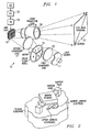
- FIG. 1 there is illustrated an overall block diagram of a digital micromirror device (DMD) display system.
- DMD digital micromirror device
- FIG. 1 an example of a DMD system 10 is illustrated, wherein the light from a light source 11 is applied through a first condenser lens 13 and through a color wheel 15, which is rotating at about sixty cycles or hertz or 60 frames per second.
- the light passing through the color wheel 15 passes through a second condenser lens 17 onto a DMD chip 19.
- the DMD chip includes an array of tiny mirror elements, or micromirrors, where each mirror element is hinged by torsion hinge and support post above a memory cell of a CMOS status RAM as shown in Fig. 2.
- the movable micromirror tilts into the on or off states by electrostatic forces based on data in the cell.
- the tilt of the mirror is either plus 10 degrees (on) or minus 10 degrees (off) to modulate the light that incident on the surface.
- the light reflected from any of the mirrors may pass through a projection lens 20 and create images on a large screen 21.
- the portion of time during which the video frame that a mirror remains in the on state determines the shade of grey.
- the time duration in which the cell is in the positive direction, or on, is represented by 8 bits of data sent to that cell.
- the color wheel 15 is divided into red, green, and blue sectors.
- the maximum red would when the red for example would be reflecting the maximum period of time as when the light is on the longest period of time in the red sector. The same would go for the other two colors.
- the minimum would be where the micromirror would not be reflecting through the color wheel and the lens, etc. at all during the color cycle.
- the intensity resolution in this pulse width modulation (PWM) is limited by the response time of the DMD mirrors.
- the total time available to display a color frame and the least time required to turn a mirror to the "on" state and back to "off” state defines the resolution of present systems.
- the most significant bit is the 7th bit with that bit representing the widest "on” time, the 6th bit being then the next widest "on” time, and the 5th bit representing the third longest “on” time, etc., all the way down to the least significant 0 bit, which is represented by the shortest time period.
- a sequential color DMD system might have 5 (five) msec (milliseconds) available for a color frame.
- the least significant bit (0 bit on only) the shortest period would be "on” for about 19.6 ⁇ s.
- the mirror on/off time would have to be less than 19.6 ⁇ s to implement this scheme with the current method.
- the DMD device In a system where the DMD device has the capability of only 6 bits, or even those that have the full eight bits, the system would have too few number of grades of grey or shades of color and therefore tend to show blockiness between portions of the picture. This would represent one of the errors that the present invention is to overcome.
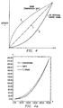
- FIG. 4a illustrates conventional degamma, SMPTE degamma, and Texas Instruments' degamma curves. This is done, for example, by each color providing the raster scanned gamma corrected red, green, or blue video data as shown in Fig. 1 using a gamma lookup table (LUT) 50 where for given input threshold levels the mirrors are turned on for given durations.
- LUT lookup table
- the output is stepped as shown in Fig. 5 rather than smooth between the thresholds of the bits and, therefore, the grade levels again take on a blockiness particularly in the low intensity regions.
- the problems of the low number of bits in the blockiness are solved by an error diffusion filter as shown in Fig. 6 for each color path (red, green, and blue) on the raster scanned video output that would normally be written into the frame RAM buffer 53.
- the filter 70 computes an error between the desired intensity of a pixel and the immediately lower achievable intensity of the DMD display. This error is then propagated into pixels to the right and below the first pixel as shown in Fig. 7.
- Fig. 6 An implementation of this filter for one color is illustrated in Fig. 6.
- the esired output for a given color is generated by a degamma lookup table (LUT) 50 at N bits of resolution and combined with errors for earlier pixels.
- the degamma LUT selected matches the appropriate curve in Fig. 4a.
- N is 12 bits addressed by 8-bits video data into the LUT 50.
- the M MSB (most significant bits) are then sent to the DMD frame buffer 53, and DMD display hardware while the N-M LSB (least significant bits) representing error are delayed for combination with later pixels.
- the error is distributed to the right and below using the four Isbs (least significant bits).
- the horizontal delay element 55 is implemented as a single N-M bit latch, while the vertical delay 57 is accomplished with an L word by N-M bit FIFO (first in first out) memory where L is the number of pixels in a video line. Both delay elements must have appropriate initialization circuitry.
- the vertical and horizontal error is divided by 2 at divider 59 and summed to the following row and column at summer 52. This filter may be accomplished with a video processor and with memory to accomplish the horizontal and vertical delays. As illustrated in Fig. 7, one-half of the error from the previous row (r-1) is provided to the row r and half of the error from the previous column (c-1) is provided to the next column (c). In this manner the error added enhances the apparent intensity resolution of the video display system.
- the FIFO memory for a video line described above can add a significant cost to the system, particularly when integrated with multiple functions in custom integrated circuits as might be desirable in high volume applications.
- only half of the pixels require half the storage that the filter mentioned above requires if the error terms least significant bits (lsbs) are shifted to the next video line from only half of the pixels.
- Fig. 8 One such filter design is illustrated in Fig. 8. The error terms from odd numbered pixel columns are shifted only horizontally, while errors from even columns shift to the next line.
- the FIFO vertical delay memory can be reduced to a length of half the number of pixels in a line.
- Fig. 9 illustrates a hardware block diagram for the filter to achieve the operation of Fig. 8.
- the pixel clock rate is divided by 2 so that every other error term is written into the vertical delay memory.
- the 12-bit output from the lookup table 51 is summed at summer 62 with the 4 least significant bits (Isbs) from the error diffusion.
- the 8 most significant bits (msb) are applied to the frame buffer.
- the lsbs (4 bits) are applied directly to multiplexer 67 and to delay 60, which are clocked by half the pixel rate by divider 61 to clockout from delay 60 the pixel data two pixels short of a full line delay.
- the output from delay 60 is applied to delay 63 and summer 65.
- Delay 63 is also clocked at the half pixel rate to add a two pixel delay to the output from delay 60.
- the output from each of the delays 60 and 63 is divided into half and applied to the other input of multiplexer 67, which alternately clocks the output from the two inputs at half the clock rate of the picture clock.
- the output from the multiplexer 67 is delayed one picture element at delay 69 that is clocked by the picture clock.
- the output from delay 69 is applied as 4 lsbs to summer 62.
- Another embodiment is illustrated in Fig. 10, wherein error added to a given or next pixel is from the error from the pixel delayed by one line delay and one pixel delay to the given pixel.
- the delays used are clocked at half the pixel clock rate to again reduce the size of the FIFO.
- a DMD display system includes an inverse gamma look-up-table (50) for converting raster scanned, gamma corrected video data of 8 bits to 12 bits inverse gamma data with 8 most significant bits (msb) and 4 least significant bits (lsb).
- the 8 msb are coupled to the micromirror of the DMD display (10) and the four lsb are delayed. For each input intensity in, the output intensity in will be displayed on the DMD device. If the degamma was perfect and there was no lack of bits, the value displayed in the DMD would be some other value N1.
- N1 was compute the difference between N and N1 and distribute this difference (error) among the neighboring pixels. The error can be distributed among the neighbors in various ways. One implementation is shown in Fig.
- a further advantage of the present invention is that the defect compensation can be performed as part of this algorithm.
- the DMD coordinates of defective pixels need to be known and the error diffusion needs to be modified to account for the fact that at those locations the pixel displays either bright (stuck ON), dark (stuck OFF) or neutral (flat pixel).
- the claimed filter is equally applicable to a three DMD system in place of the color wheeL
- the degamma lookup table may be different for the three primary colors.
Landscapes
- Engineering & Computer Science (AREA)
- Multimedia (AREA)
- Signal Processing (AREA)
- Computer Hardware Design (AREA)
- Crystallography & Structural Chemistry (AREA)
- Physics & Mathematics (AREA)
- Chemical & Material Sciences (AREA)
- General Physics & Mathematics (AREA)
- Theoretical Computer Science (AREA)
- Mechanical Light Control Or Optical Switches (AREA)
- Projection Apparatus (AREA)
- Control Of Indicators Other Than Cathode Ray Tubes (AREA)
- Transforming Electric Information Into Light Information (AREA)
Description
- This invention relates to digital imaging and more particularly to an error diffusion filter for a digital micromirror device (DMD) display as defined in the precharacterizing portion of
claim 1. - A new projection display that utilizes reflections from hundreds of thousands of micromirrors, each mounted above its own semiconductor memory cell is described in IEEE Spectrum, November 1993, vol. 30, no. 11, written by Jack M. Younse of Texas Instruments Incorporated. The digital micromirror device (DMD) comprises a special light modulator that was invented in 1987 by Larry J. Hornbeck, a Texas Instruments Incorporated scientist. The DMD, or digital micromirror device covers each memory cell of a CMOS static RAM with a movable micromirror. Electrostatic forces based on the data in this cell tilt the mirror either plus or minus 10 degrees, modulating the light incident on the surface. The light reflected from any of the mirrors passes through a projection lens and creates an image on a large screen. Light from the remaining off mirrors is reflected away from the projection lens and trapped. The portion of the time during each video frame that the mirror remains in the on state determines the shades of grey- from black for zero on time to white for 100 percent on time. Color may be added in two ways, by a color wheel or a 3-DMD set up.
- Some DMD devices may have the capability to display only a low number of bits representing the on and off times and, therefore, the shades of grey or shades of color, leading to degradation of the video quality. Also, the use of digital degamma in the DMD display systems entails some loss of resolution (blockiness) in the low intensity regions. Finally, even the best of DMDs can have some defects (pixels stuck on, off, or flat). It is desirable to find some method to provide a correction for these display errors and to provide a more pleasing picture without significantly increasing the time for processing by increasing the number of bits for each on or off time.
- An error diffusion filter of the type defined in the precharacterizing portion of
claim 1 is known from WO-A-9209064. Using that error diffusion filter, durations of less than the shortest displayable duration can be displayed by adjusting the turn-on time of a proportion of the adjacent mirrors. - In accordance with one preferred embodiment of the present invention, an error diffusion filter for a DMD display comprises the features of
claim 1. - Reference will now be made, by way of example, to the accompanying drawings, in which:
- Fig. 1 is an overall block diagram of a Digital Micromirror Display System;
- Fig. 2 is a sketch of a micromirror element in Fig. 1 ;
- Fig. 3 is a timing diagram illustrating the on-time of MSB and LSB;
- Fig. 4 is a sketch of CRT response, gamma transmission sent, and inverse gamma;
- Fig. 4a is a more detailed plot of the degamma for conventional degamma, SMPTE degamma and Texas Instruments' degamma.
- Fig. 5 illustrates the stepped DMD response with lookup table (LUT);
- Fig. 6 is a sketch of an error diffusion filter;
- Fig. 7 illustrates the operation of the filter of Fig. 6;
- Fig. 8 illustrates the operation in accordance with one embodiment of the invention where added numbered pixel columns are shifted horizontally, while the errors from even columns are shifted to the next line;
- Fig. 9 illustrates a hardwere block diagram for the operation of Fig. 8; and
- Fig. 10 illustrates the operation of another embodiment using half cycle delay times;
-
- Referring to Fig. 1, there is illustrated an overall block diagram of a digital micromirror device (DMD) display system. Referring to Fig. 1, an example of a
DMD system 10 is illustrated, wherein the light from alight source 11 is applied through afirst condenser lens 13 and through acolor wheel 15, which is rotating at about sixty cycles or hertz or 60 frames per second. The light passing through thecolor wheel 15 passes through asecond condenser lens 17 onto aDMD chip 19. The DMD chip includes an array of tiny mirror elements, or micromirrors, where each mirror element is hinged by torsion hinge and support post above a memory cell of a CMOS status RAM as shown in Fig. 2. The movable micromirror tilts into the on or off states by electrostatic forces based on data in the cell. The tilt of the mirror is either plus 10 degrees (on) or minus 10 degrees (off) to modulate the light that incident on the surface. For additional details, see U.S. Patent No. 5,061,049 entitled, "Spatial Light Modulator" and U.S. Patent No. 5,280,277 entitled, "Field Updated Deferrable Mirror Device," both of Larry J. Hornbeck. As shown, the light reflected from any of the mirrors may pass through aprojection lens 20 and create images on alarge screen 21. As stated previously, the portion of time during which the video frame that a mirror remains in the on state determines the shade of grey. The time duration in which the cell is in the positive direction, or on, is represented by 8 bits of data sent to that cell. Thecolor wheel 15 is divided into red, green, and blue sectors. In the color wheel example, the maximum red would when the red for example would be reflecting the maximum period of time as when the light is on the longest period of time in the red sector. The same would go for the other two colors. The minimum would be where the micromirror would not be reflecting through the color wheel and the lens, etc. at all during the color cycle. The intensity resolution in this pulse width modulation (PWM) is limited by the response time of the DMD mirrors. The total time available to display a color frame and the least time required to turn a mirror to the "on" state and back to "off" state defines the resolution of present systems. In the arrangement for the 8 bits, the most significant bit, as illustrated in Fig. 3, is the 7th bit with that bit representing the widest "on" time, the 6th bit being then the next widest "on" time, and the 5th bit representing the third longest "on" time, etc., all the way down to the least significant 0 bit, which is represented by the shortest time period. For example, a sequential color DMD system might have 5 (five) msec (milliseconds) available for a color frame. For 8-bit binary PWM, the least significant bit (0 bit on only), the shortest period would be "on" for about 19.6 µs. The mirror on/off time would have to be less than 19.6 µs to implement this scheme with the current method. In a system where the DMD device has the capability of only 6 bits, or even those that have the full eight bits, the system would have too few number of grades of grey or shades of color and therefore tend to show blockiness between portions of the picture. This would represent one of the errors that the present invention is to overcome. - Another error is due to the degamma effect in the display. On a typical CRT television display system, the intensity of the picture is a function of the voltage, which is represented by the CRT response in Curve A of Fig. 4. Note that the intensity for the lower voltage is nearly flat in the low voltage region, but increases rapidly at middle to highest voltage inputs. In order to correct for this, the transmission that is sent to the display has a gamma characteristic of curve B so that the overall response is linear as represented by the linear solid line C. In order to duplicate the CRT response for the digital micromirror device, a digital degamma characteristic is made to follow curve A of Fig. 4. Fig. 4a illustrates conventional degamma, SMPTE degamma, and Texas Instruments' degamma curves. This is done, for example, by each color providing the raster scanned gamma corrected red, green, or blue video data as shown in Fig. 1 using a gamma lookup table (LUT) 50 where for given input threshold levels the mirrors are turned on for given durations. However, due to the
gamma LUT 50 being digital in nature the output is stepped as shown in Fig. 5 rather than smooth between the thresholds of the bits and, therefore, the grade levels again take on a blockiness particularly in the low intensity regions. - The problems of the low number of bits in the blockiness are solved by an error diffusion filter as shown in Fig. 6 for each color path (red, green, and blue) on the raster scanned video output that would normally be written into the
frame RAM buffer 53. Thefilter 70 computes an error between the desired intensity of a pixel and the immediately lower achievable intensity of the DMD display. This error is then propagated into pixels to the right and below the first pixel as shown in Fig. 7. - An implementation of this filter for one color is illustrated in Fig. 6. The esired output for a given color is generated by a degamma lookup table (LUT) 50 at N bits of resolution and combined with errors for earlier pixels. The degamma LUT selected matches the appropriate curve in Fig. 4a. N is 12 bits addressed by 8-bits video data into the
LUT 50. The M MSB (most significant bits) are then sent to theDMD frame buffer 53, and DMD display hardware while the N-M LSB (least significant bits) representing error are delayed for combination with later pixels. In this embodiment, M equals 8-bits and N-M = 4 lsb (least significant bits). The error is distributed to the right and below using the four Isbs (least significant bits). Thehorizontal delay element 55 is implemented as a single N-M bit latch, while thevertical delay 57 is accomplished with an L word by N-M bit FIFO (first in first out) memory where L is the number of pixels in a video line. Both delay elements must have appropriate initialization circuitry. The vertical and horizontal error is divided by 2 atdivider 59 and summed to the following row and column atsummer 52. This filter may be accomplished with a video processor and with memory to accomplish the horizontal and vertical delays. As illustrated in Fig. 7, one-half of the error from the previous row (r-1) is provided to the row r and half of the error from the previous column (c-1) is provided to the next column (c). In this manner the error added enhances the apparent intensity resolution of the video display system. - The FIFO memory for a video line described above can add a significant cost to the system, particularly when integrated with multiple functions in custom integrated circuits as might be desirable in high volume applications. In accordance with the present invention, only half of the pixels require half the storage that the filter mentioned above requires if the error terms least significant bits (lsbs) are shifted to the next video line from only half of the pixels. One such filter design is illustrated in Fig. 8. The error terms from odd numbered pixel columns are shifted only horizontally, while errors from even columns shift to the next line. As a result, the FIFO vertical delay memory can be reduced to a length of half the number of pixels in a line. Fig. 9 illustrates a hardware block diagram for the filter to achieve the operation of Fig. 8. The pixel clock rate is divided by 2 so that every other error term is written into the vertical delay memory. The 12-bit output from the lookup table 51 is summed at
summer 62 with the 4 least significant bits (Isbs) from the error diffusion. The 8 most significant bits (msb) are applied to the frame buffer. The lsbs (4 bits) are applied directly tomultiplexer 67 and to delay 60, which are clocked by half the pixel rate bydivider 61 to clockout fromdelay 60 the pixel data two pixels short of a full line delay. The output fromdelay 60 is applied to delay 63 andsummer 65.Delay 63 is also clocked at the half pixel rate to add a two pixel delay to the output fromdelay 60. The output from each of thedelays multiplexer 67, which alternately clocks the output from the two inputs at half the clock rate of the picture clock. The output from themultiplexer 67 is delayed one picture element atdelay 69 that is clocked by the picture clock. The output fromdelay 69 is applied as 4 lsbs tosummer 62. Another embodiment is illustrated in Fig. 10, wherein error added to a given or next pixel is from the error from the pixel delayed by one line delay and one pixel delay to the given pixel. The delays used are clocked at half the pixel clock rate to again reduce the size of the FIFO. - A DMD display system includes an inverse gamma look-up-table (50) for converting raster scanned, gamma corrected video data of 8 bits to 12 bits inverse gamma data with 8 most significant bits (msb) and 4 least significant bits (lsb). The 8 msb are coupled to the micromirror of the DMD display (10) and the four lsb are delayed. For each input intensity in, the output intensity in will be displayed on the DMD device. If the degamma was perfect and there was no lack of bits, the value displayed in the DMD would be some other value N1. We compute the difference between N and N1 and distribute this difference (error) among the neighboring pixels. The error can be distributed among the neighbors in various ways. One implementation is shown in Fig. 8. A further advantage of the present invention is that the defect compensation can be performed as part of this algorithm. For this, the DMD coordinates of defective pixels need to be known and the error diffusion needs to be modified to account for the fact that at those locations the pixel displays either bright (stuck ON), dark (stuck OFF) or neutral (flat pixel).
- Although the DMD system described uses a color wheel the claimed filter is equally applicable to a three DMD system in place of the color wheeL The degamma lookup table may be different for the three primary colors.
Claims (4)
- An error diffusion filter (70) for enhancing the apparent intensity resolution of a digital micromirror device display (19) comprising an array of micromirrors and being driven by a raster scanned video signal representing a plurality of video lines (r-1, r, r+1) representing a plurality of pixels, said filter comprising means for determining the intensity error value of a pixel, which is defined as the difference between the desired intensity of the pixel given according to said raster scanned video signal and the closest lower intensity achievable by the micromirror corresponding to said given pixel, over the entire range of intensities; and means including a vertical delay memory (60, 63) for propagating said intensity error values to the pixels of the next video line (r, r+1) from only half of the pixels of the present video line (r-1, r);
characterized in that the error values from every second pixel of the present video line (r-1, r) are shifted horizontally within said video line (r-1, r) by a horizontal delay memory (69) while error values from the pixels between said every second pixel of said video line (r-1, r) are shifted to the pixels of the next video line (r, r+1) via said vertical delay memory (60, 63). - The filter of claim 1 wherein the pixel clock rate of the vertical delay memory (60, 63) is divided in half so that every second errors value is written into the vertical delay memory (60, 63).
- A digital micromirror device display system comprising:an error diffusion filter (70) according to claim 1 or claim 2;a light source (11);a digital micromirror device (19) comprising an array of micromirrors arranged in columns and rows mounted above a corresponding array of semiconductor memory devices whereupon by operations of the memory devices the micromirrors are made to reflect light from said light source (11) in a desired direction and the duration of the reflected light at any given micromirror provides the pixel intensity from that micromirror;a source of a first set of raster scan data for operating said micromirrors using said memory devices for a time duration dependent on the data; anda degamma lookup table LUT (50) responsive to said source of a first set of raster scan data for providing a second set of raster scan data with most significant bits of said second scan data for each given micromirror representing the closest achievable intensity to the desired intensity at said given micromirror without exceeding the desired intensity and with least significant bits of said second scan data for each given micromirror representing intensity added to adjacent micromirrors to achieve an apparent intensity at said given micromirror equal to said desired intensity; whereinsaid error diffusion filter (70) is coupled between said lookup table LUT (50) and said digital micromirror device (19) for propagating bits to said micromirrors to achieve said apparent intensity comprising:summing means 62) for summing said most significant bits with delayed least significant bits from said given micromirror;means for coupling said most significant bits from said summing means 62) to said micromirrors and said least significant bits to delay means (60, 63, 69); andmeans for coupling the output of said delay means (60, 63, 69) to said summing means (62) to add said least significant bits from said given micromirrors to micromirrors adjacent said given micromirror; and said delay means (60, 63, 69) delaying said least significant bits such that said least significant bits are added to the most significant bits for said adjacent micromirrors.
- The digital micromirror device display system of claim 3 wherein said vertical delays (60, 63) is a FIFO memory with a length equal to half the number of pixels in a video line (r-1, r, r+1).
Applications Claiming Priority (2)
| Application Number | Priority Date | Filing Date | Title |
|---|---|---|---|
| US315457 | 1994-09-30 | ||
| US08/315,457 US5726718A (en) | 1994-09-30 | 1994-09-30 | Error diffusion filter for DMD display |
Publications (3)
| Publication Number | Publication Date |
|---|---|
| EP0704835A2 EP0704835A2 (en) | 1996-04-03 |
| EP0704835A3 EP0704835A3 (en) | 1996-05-22 |
| EP0704835B1 true EP0704835B1 (en) | 2005-02-09 |
Family
ID=23224520
Family Applications (1)
| Application Number | Title | Priority Date | Filing Date |
|---|---|---|---|
| EP95114890A Expired - Lifetime EP0704835B1 (en) | 1994-09-30 | 1995-09-21 | Error diffusion filter for DMD display |
Country Status (5)
| Country | Link |
|---|---|
| US (1) | US5726718A (en) |
| EP (1) | EP0704835B1 (en) |
| JP (1) | JPH08214244A (en) |
| KR (1) | KR100426917B1 (en) |
| DE (1) | DE69534001D1 (en) |
Families Citing this family (28)
| Publication number | Priority date | Publication date | Assignee | Title |
|---|---|---|---|---|
| US5592188A (en) | 1995-01-04 | 1997-01-07 | Texas Instruments Incorporated | Method and system for accentuating intense white display areas in sequential DMD video systems |
| US6052491A (en) * | 1996-01-26 | 2000-04-18 | Texas Instruments Incorporated | Non-monotonic contour diffusion and algorithm |
| US6342898B1 (en) * | 1998-03-16 | 2002-01-29 | Texas Instruments Incorporated | Compression and decompression of degamma tables for projection systems |
| US6271957B1 (en) * | 1998-05-29 | 2001-08-07 | Affymetrix, Inc. | Methods involving direct write optical lithography |
| US6657758B1 (en) | 1998-06-04 | 2003-12-02 | Board Of Regents, The University Of Texas System | Variable spectrum generator system |
| JP4016493B2 (en) | 1998-08-05 | 2007-12-05 | 三菱電機株式会社 | Display device and multi-gradation circuit thereof |
| US6583921B2 (en) * | 1999-12-28 | 2003-06-24 | Texas Instruments Incorporated | Micromechanical device and method for non-contacting edge-coupled operation |
| KR100371557B1 (en) * | 2000-02-26 | 2003-02-14 | 조헌영 | Modification methods of the physical properties of mid sole with leather shaving dust |
| KR100806056B1 (en) * | 2000-04-25 | 2008-02-21 | 코닌클리케 필립스 일렉트로닉스 엔.브이. | Method of reducing errors in displays using double-line sub-field addressing |
| JP4641334B2 (en) * | 2000-07-18 | 2011-03-02 | キヤノン株式会社 | Image display device |
| JP5127089B2 (en) | 2000-10-17 | 2013-01-23 | キヤノン株式会社 | Display device, projection display device, light modulation device driving device, and light modulation device driving method |
| KR100434293B1 (en) * | 2002-01-09 | 2004-06-05 | 엘지전자 주식회사 | Gamma Correction Device Using Linear Interpolation |
| KR100434294B1 (en) * | 2002-01-09 | 2004-06-05 | 엘지전자 주식회사 | Gamma Correction Device |
| US7098927B2 (en) * | 2002-02-01 | 2006-08-29 | Sharp Laboratories Of America, Inc | Methods and systems for adaptive dither structures |
| US7295345B2 (en) * | 2003-04-29 | 2007-11-13 | Eastman Kodak Company | Method for calibration independent defect correction in an imaging system |
| CA2526467C (en) * | 2003-05-20 | 2015-03-03 | Kagutech Ltd. | Digital backplane recursive feedback control |
| US7701519B2 (en) * | 2003-06-19 | 2010-04-20 | Texas Instruments Incorporated | Display system and signal processing using diamond-shaped DMDs |
| KR100508936B1 (en) * | 2003-08-12 | 2005-08-17 | 삼성에스디아이 주식회사 | Method capable of performing high-speed error diffusion and palasma display panel driving apparatus using the same |
| US8243093B2 (en) * | 2003-08-22 | 2012-08-14 | Sharp Laboratories Of America, Inc. | Systems and methods for dither structure creation and application for reducing the visibility of contouring artifacts in still and video images |
| US7352373B2 (en) * | 2003-09-30 | 2008-04-01 | Sharp Laboratories Of America, Inc. | Systems and methods for multi-dimensional dither structure creation and application |
| US7164397B2 (en) * | 2003-09-30 | 2007-01-16 | Texas Instruments Incorporated | Discrete light color processor |
| US7474316B2 (en) * | 2004-08-17 | 2009-01-06 | Sharp Laboratories Of America, Inc. | Bit-depth extension of digital displays via the use of models of the impulse response of the visual system |
| JP5586831B2 (en) | 2004-11-10 | 2014-09-10 | トムソン ライセンシング | System and method for dark noise reduction in pulse width modulation (PWM) displays |
| US20060132471A1 (en) * | 2004-12-17 | 2006-06-22 | Paul Winer | Illumination modulation technique |
| JP2007101960A (en) * | 2005-10-05 | 2007-04-19 | Fujitsu Hitachi Plasma Display Ltd | Display method of digital display device, and digital display device |
| FR2936817B1 (en) * | 2008-10-07 | 2013-07-19 | Varel Europ | PROCESS FOR MANUFACTURING A WORKPIECE COMPRISING A BLOCK OF DENSE MATERIAL OF THE CEMENT CARBIDE TYPE, HAVING A LARGE NUMBER OF PROPERTIES AND PIECE OBTAINED |
| JP2012134912A (en) * | 2010-12-24 | 2012-07-12 | Seiko Epson Corp | Image processing device, image processing method and image processing program |
| US20130135338A1 (en) * | 2011-11-30 | 2013-05-30 | Qualcomm Mems Technologies, Inc. | Method and system for subpixel-level image multitoning |
Family Cites Families (5)
| Publication number | Priority date | Publication date | Assignee | Title |
|---|---|---|---|---|
| JPS6163893A (en) * | 1984-09-06 | 1986-04-02 | 株式会社日立製作所 | Display of false halftone image of display unit |
| US5201030A (en) * | 1989-09-28 | 1993-04-06 | Sun Microsystems, Inc. | Method and apparatus for dithering graphic images |
| GB9024978D0 (en) * | 1990-11-16 | 1991-01-02 | Rank Cintel Ltd | Digital mirror spatial light modulator |
| JPH0772824B2 (en) * | 1991-12-03 | 1995-08-02 | インターナショナル・ビジネス・マシーンズ・コーポレイション | Display system |
| US5452024A (en) * | 1993-11-01 | 1995-09-19 | Texas Instruments Incorporated | DMD display system |
-
1994
- 1994-09-30 US US08/315,457 patent/US5726718A/en not_active Expired - Lifetime
-
1995
- 1995-09-21 DE DE69534001T patent/DE69534001D1/en not_active Expired - Lifetime
- 1995-09-21 EP EP95114890A patent/EP0704835B1/en not_active Expired - Lifetime
- 1995-09-29 KR KR1019950032772A patent/KR100426917B1/en not_active IP Right Cessation
- 1995-09-29 JP JP7253962A patent/JPH08214244A/en active Pending
Non-Patent Citations (1)
| Title |
|---|
| IEEE SPECTRUM, vol. 30, no. 11, November 1993 (1993-11-01), pages 27 - 31 * |
Also Published As
| Publication number | Publication date |
|---|---|
| KR960011367A (en) | 1996-04-20 |
| EP0704835A2 (en) | 1996-04-03 |
| US5726718A (en) | 1998-03-10 |
| KR100426917B1 (en) | 2004-06-16 |
| DE69534001D1 (en) | 2005-03-17 |
| JPH08214244A (en) | 1996-08-20 |
| EP0704835A3 (en) | 1996-05-22 |
Similar Documents
| Publication | Publication Date | Title |
|---|---|---|
| EP0704835B1 (en) | Error diffusion filter for DMD display | |
| US5623281A (en) | Error diffusion filter for DMD display | |
| EP0823698B1 (en) | Improvements in or relating to digital micromirror display systems | |
| JP4215287B2 (en) | Video display system and addressing method thereof | |
| JP4077890B2 (en) | Artifact reduction method in image display system | |
| KR100346877B1 (en) | Method for Reducing Temporal Artifacts in Digital Video Systems | |
| EP1269756B1 (en) | Improvements in dmd-based image display systems | |
| US5497172A (en) | Pulse width modulation for spatial light modulator with split reset addressing | |
| US6008785A (en) | Generating load/reset sequences for spatial light modulator | |
| CA2193422C (en) | Dmd-based projector for institutional use | |
| US8717394B2 (en) | Boundary dispersion for mitigating PWM temporal contouring artifacts in digital displays | |
| US7471273B2 (en) | Bit segment timing organization providing flexible bit segment lengths | |
| US6226054B1 (en) | Global light boost for pulse width modulation display systems | |
| EP0755556B1 (en) | Display device driving circuitry and method | |
| US7161608B2 (en) | Digital system and method for displaying images using shifted bit-weights for neutral density filtering applications | |
| US9344694B2 (en) | Spatial light modulator sub-pixel architecture and method | |
| US7403187B2 (en) | Generalized reset conflict resolution of load/reset sequences for spatial light modulators | |
| EP0686954B1 (en) | Non binary pulse width modulation method for spatial light modulator | |
| JP2002032049A (en) | Picture display device |
Legal Events
| Date | Code | Title | Description |
|---|---|---|---|
| PUAI | Public reference made under article 153(3) epc to a published international application that has entered the european phase |
Free format text: ORIGINAL CODE: 0009012 |
|
| AK | Designated contracting states |
Kind code of ref document: A2 Designated state(s): DE FR GB IT NL |
|
| PUAL | Search report despatched |
Free format text: ORIGINAL CODE: 0009013 |
|
| AK | Designated contracting states |
Kind code of ref document: A3 Designated state(s): DE FR GB IT NL |
|
| K1C1 | Correction of patent application (title page) published |
Effective date: 19960403 |
|
| 17P | Request for examination filed |
Effective date: 19961121 |
|
| 17Q | First examination report despatched |
Effective date: 20000324 |
|
| GRAP | Despatch of communication of intention to grant a patent |
Free format text: ORIGINAL CODE: EPIDOSNIGR1 |
|
| GRAS | Grant fee paid |
Free format text: ORIGINAL CODE: EPIDOSNIGR3 |
|
| GRAA | (expected) grant |
Free format text: ORIGINAL CODE: 0009210 |
|
| AK | Designated contracting states |
Kind code of ref document: B1 Designated state(s): DE FR GB IT NL |
|
| PG25 | Lapsed in a contracting state [announced via postgrant information from national office to epo] |
Ref country code: NL Free format text: LAPSE BECAUSE OF FAILURE TO SUBMIT A TRANSLATION OF THE DESCRIPTION OR TO PAY THE FEE WITHIN THE PRESCRIBED TIME-LIMIT Effective date: 20050209 Ref country code: IT Free format text: LAPSE BECAUSE OF FAILURE TO SUBMIT A TRANSLATION OF THE DESCRIPTION OR TO PAY THE FEE WITHIN THE PRESCRIBED TIME-LIMIT;WARNING: LAPSES OF ITALIAN PATENTS WITH EFFECTIVE DATE BEFORE 2007 MAY HAVE OCCURRED AT ANY TIME BEFORE 2007. THE CORRECT EFFECTIVE DATE MAY BE DIFFERENT FROM THE ONE RECORDED. Effective date: 20050209 Ref country code: FR Free format text: LAPSE BECAUSE OF NON-PAYMENT OF DUE FEES Effective date: 20050209 |
|
| REG | Reference to a national code |
Ref country code: GB Ref legal event code: FG4D |
|
| REF | Corresponds to: |
Ref document number: 69534001 Country of ref document: DE Date of ref document: 20050317 Kind code of ref document: P |
|
| PG25 | Lapsed in a contracting state [announced via postgrant information from national office to epo] |
Ref country code: DE Free format text: LAPSE BECAUSE OF FAILURE TO SUBMIT A TRANSLATION OF THE DESCRIPTION OR TO PAY THE FEE WITHIN THE PRESCRIBED TIME-LIMIT Effective date: 20050510 |
|
| NLV1 | Nl: lapsed or annulled due to failure to fulfill the requirements of art. 29p and 29m of the patents act | ||
| PLBE | No opposition filed within time limit |
Free format text: ORIGINAL CODE: 0009261 |
|
| STAA | Information on the status of an ep patent application or granted ep patent |
Free format text: STATUS: NO OPPOSITION FILED WITHIN TIME LIMIT |
|
| 26N | No opposition filed |
Effective date: 20051110 |
|
| EN | Fr: translation not filed | ||
| PGFP | Annual fee paid to national office [announced via postgrant information from national office to epo] |
Ref country code: GB Payment date: 20100809 Year of fee payment: 16 |
|
| GBPC | Gb: european patent ceased through non-payment of renewal fee |
Effective date: 20110921 |
|
| PG25 | Lapsed in a contracting state [announced via postgrant information from national office to epo] |
Ref country code: GB Free format text: LAPSE BECAUSE OF NON-PAYMENT OF DUE FEES Effective date: 20110921 |