EP0683404B1 - Method and apparatus for producing diffraction gratings by machine forming in a fast operation cycle - Google Patents
Method and apparatus for producing diffraction gratings by machine forming in a fast operation cycle Download PDFInfo
- Publication number
- EP0683404B1 EP0683404B1 EP19940830166 EP94830166A EP0683404B1 EP 0683404 B1 EP0683404 B1 EP 0683404B1 EP 19940830166 EP19940830166 EP 19940830166 EP 94830166 A EP94830166 A EP 94830166A EP 0683404 B1 EP0683404 B1 EP 0683404B1
- Authority
- EP
- European Patent Office
- Prior art keywords
- substrate
- tool
- punching
- translation
- punching tool
- Prior art date
- Legal status (The legal status is an assumption and is not a legal conclusion. Google has not performed a legal analysis and makes no representation as to the accuracy of the status listed.)
- Expired - Lifetime
Links
Images
Classifications
-
- G—PHYSICS
- G02—OPTICS
- G02B—OPTICAL ELEMENTS, SYSTEMS OR APPARATUS
- G02B5/00—Optical elements other than lenses
- G02B5/18—Diffraction gratings
- G02B5/1847—Manufacturing methods
- G02B5/1852—Manufacturing methods using mechanical means, e.g. ruling with diamond tool, moulding
Definitions
- the present invention relates to the field of the advanced optical technology and more particularly a method of producing diffraction gratings by machine forming in a fast operation cycle. This invention also relates to an apparatus for carrying out such method.
- said known process is intended for embossing a pattern having a microscopic relief structure, such as an optical diffraction grating, onto a layer od thermoplastic material. Therefore, the method and apparatus disclosed in EP 0169326 are intended to plastically mould a thermoplastic layer having a predetermined optical diffraction grating, and are not able to create an optical diffraction grating.
- the present invention aims at providing a method and a device of the above-mentioned type for producing diffraction gratings in a considerably lower time than that required by the conventional mechanical and/or photomechanical techniques of the present state of art.
- a method is provided consisting of the following steps: arranging a solid or added metal substrate on a displaceable means which moves at a controlled speed; and carrying out on said substrate a succession of sizing operations by a punching tool combined with a piezoelectric actuator so as to produce on said substrate a series of grooves forming the desired grating.
- said punching tool is formed of a fixture provided with an active wedge-shaped diamond point having a rectilinear cutting edge arranged transversally to the displacement direction of the movable carriage of the substrate.
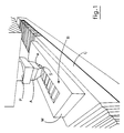
- Fig. 1 is a schematic perspective view of the apparatus for carrying out the method according to the invention.
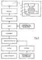
- Fig. 2 is a block diagram of the control assembly of the apparatus of Fig. 1.
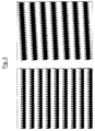
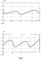
- Figs. 3 and 4 show the results of some characteristic tests of the invention.
- a wedge-shaped diamond point tool A machined with a determined angle is fixedly attached to a piezoelectric actuator P capable of carrying out a vertical micrometrically controlled displacement with a high repetition frequency.
- Diamond A is arranged with a horizontally aligned cutting edge S.
- Translation carriage C slides under tool A horizontally and transversally with respect to cutting edge S of the tool, said carriage carrying a metal substrate M having a surface B, on which the grating is cut, which has been formerly machined with optical finish and carefully positioned with respect to the edge of the tool.
- v the sliding speed of substrate M
- f the operation frequency of the piezoelectric actuator P.
- FIG. 2 A block diagram of the control assembly of the described apparatus is shown in Fig. 2.
- the invention allows a number of advantages to be achieved with respect to the already known techniques, among which a higher production speed which entails a considerable reduction of the cost of the end product, and a high capability of controlling the operating parameters with the result of a high flexibility as far as the type of the produced components is concerned.
- Fig. 3 shows two interference diagrams obtained by interferometer microscope and concerning the profile of gratings provided by the above-mentioned method
- Fig. 4 shows the profile of a grating detected by a mechanical high-resolution profilometer.
- the invention may be advantageously applied to the production of a large range of advanced optical components such as the diffraction gratings having varying spacing, which find application in the VUV spectroscopy and soft X-rays.
- advanced optical components such as the diffraction gratings having varying spacing, which find application in the VUV spectroscopy and soft X-rays.
- Such gratings can be particularly used in the field of the analysis of the synchrotron radiations and in the space applications as well.
Landscapes
- Physics & Mathematics (AREA)
- Engineering & Computer Science (AREA)
- Manufacturing & Machinery (AREA)
- General Physics & Mathematics (AREA)
- Optics & Photonics (AREA)
- Diffracting Gratings Or Hologram Optical Elements (AREA)
Description
- The present invention relates to the field of the advanced optical technology and more particularly a method of producing diffraction gratings by machine forming in a fast operation cycle. This invention also relates to an apparatus for carrying out such method.
- It is known, from document EP 0169326, a process for the production of a macroscopic surface pattern with a microscopic structure, in particular a structure which has an optical-diffraction effect, by bulding selected surface regions of an embossing die having a microstructure into a thermoplastic layer, characterised in that a ray source is used to heat an approximately punctiform element of the surface of the thermoplastic layer. Said element lies in the focal spot of the ray source, so that the microstructure of the embossing die is plastically moulded only in said element of the surface of the thermoplastic layer, and that the surface pattern is composed of a plurality of such elements of the surface.
In other words, said known process (and apparatus) is intended for embossing a pattern having a microscopic relief structure, such as an optical diffraction grating, onto a layer od thermoplastic material.
Therefore, the method and apparatus disclosed in EP 0169326 are intended to plastically mould a thermoplastic layer having a predetermined optical diffraction grating, and are not able to create an optical diffraction grating. - The present invention aims at providing a method and a device of the above-mentioned type for producing diffraction gratings in a considerably lower time than that required by the conventional mechanical and/or photomechanical techniques of the present state of art.
According to the invention a method is provided consisting of the following steps: arranging a solid or added metal substrate on a displaceable means which moves at a controlled speed; and carrying out on said substrate a succession of sizing operations by a punching tool combined with a piezoelectric actuator so as to produce on said substrate a series of grooves forming the desired grating.
Still according to the invention said punching tool is formed of a fixture provided with an active wedge-shaped diamond point having a rectilinear cutting edge arranged transversally to the displacement direction of the movable carriage of the substrate. - This invention will now be described with reference to the accompanying drawings which show by way of an illustrative, non-limitative example a preferred embodiment of the invention.
- In the drawings:
- Fig. 1 is a schematic perspective view of the apparatus for carrying out the method according to the invention.
- Fig. 2 is a block diagram of the control assembly of the apparatus of Fig. 1.
- Figs. 3 and 4 show the results of some characteristic tests of the invention.
- With reference to Fig. 1, a wedge-shaped diamond point tool A machined with a determined angle is fixedly attached to a piezoelectric actuator P capable of carrying out a vertical micrometrically controlled displacement with a high repetition frequency. Diamond A is arranged with a horizontally aligned cutting edge S.
Translation carriage C slides under tool A horizontally and transversally with respect to cutting edge S of the tool, said carriage carrying a metal substrate M having a surface B, on which the grating is cut, which has been formerly machined with optical finish and carefully positioned with respect to the edge of the tool.
The combined movements of tool A and substrate M produces a succession of rectilinear, parallel cuts I (forming the grooves of the grating) spaced by a gap of p = v/f, where v is the sliding speed of substrate M, and f is the operation frequency of the piezoelectric actuator P. By varying v during the cutting step, gratings having varying spacing may be produced.
Also the depth of cuts I can be varied by a suitable modification of the diamond point A and the operating characteristics of piezoelectric actuator P. - A block diagram of the control assembly of the described apparatus is shown in Fig. 2.
- The invention allows a number of advantages to be achieved with respect to the already known techniques, among which a higher production speed which entails a considerable reduction of the cost of the end product, and a high capability of controlling the operating parameters with the result of a high flexibility as far as the type of the produced components is concerned.
- Fig. 3 shows two interference diagrams obtained by interferometer microscope and concerning the profile of gratings provided by the above-mentioned method, and Fig. 4 shows the profile of a grating detected by a mechanical high-resolution profilometer.
- The invention may be advantageously applied to the production of a large range of advanced optical components such as the diffraction gratings having varying spacing, which find application in the VUV spectroscopy and soft X-rays. Such gratings can be particularly used in the field of the analysis of the synchrotron radiations and in the space applications as well.
- The present invention has been illustrated and described with reference to a preferred embodiment thereof, however it should be understood that construction and/or operating modifications can be in practice made by those skilled in the art without departing from the scope of the present invention.
Claims (7)
- A method of producing diffraction gratings, comprising the steps of arranging the substrate, on which the grating grooves are to be produced, on a translation means, having a controlled speed of traslation, providing said grooves by repetitively punching with a tool moving with respect to the substrate;
characterized in that:
each step of punching comprises punching the substrate directly with a wedge-shaped diamond edge of said tool, while controlling the translation of the substrate with regard to said punching tool, so as to provide one groove at any stroke of the tool on the surface. - A method according to claim 1, characterized in that the translational speed of the substrate can be changed during the translation of the substrate with respect to the punching tool so as to provide corresponding variations of the gap between the grating grooves.
- A method according to claims 1 and 2, characterized in that the punching tool moves vertically.
- A method according to claims 1 to 3, characterized in that the method comprises providing the punching tool with a wedge-shaped diamond edge having the edge arranged perpendicularly to the sliding direction of the carriage carrying the substrate.
- A method according to claims 1 to 4, characterized in orienting the substrate formed of a solid body and having a surface with optical finish so that said surface faces the punching tool.
- An apparatus for carrying out the method according to claims 1 and 2, where the apparatus comprises:a) a punching tool provided with a wedge-shaped diamond edge;b) a piezoelectric actuator arranged for driving the punching tool;c) an electronic assembly arranged for controlling the actuator;d) a translation system arranged for carrying the substrate;e) control means arranged for controlling the speed of the translation of the substrate, wherein the electronic assembly and control means are arranged so as to provide one groove at any stroke of the tool on the surface of the substrate.
- An apparatus according to claim 6, characterized in that said the electronic assembly is an electro-optical assembly.
Priority Applications (2)
| Application Number | Priority Date | Filing Date | Title |
|---|---|---|---|
| DE69421519T DE69421519D1 (en) | 1994-04-08 | 1994-04-08 | Process and device for the production of diffraction gratings in a fast processing system |
| EP19940830166 EP0683404B1 (en) | 1994-04-08 | 1994-04-08 | Method and apparatus for producing diffraction gratings by machine forming in a fast operation cycle |
Applications Claiming Priority (1)
| Application Number | Priority Date | Filing Date | Title |
|---|---|---|---|
| EP19940830166 EP0683404B1 (en) | 1994-04-08 | 1994-04-08 | Method and apparatus for producing diffraction gratings by machine forming in a fast operation cycle |
Publications (2)
| Publication Number | Publication Date |
|---|---|
| EP0683404A1 EP0683404A1 (en) | 1995-11-22 |
| EP0683404B1 true EP0683404B1 (en) | 1999-11-03 |
Family
ID=8218420
Family Applications (1)
| Application Number | Title | Priority Date | Filing Date |
|---|---|---|---|
| EP19940830166 Expired - Lifetime EP0683404B1 (en) | 1994-04-08 | 1994-04-08 | Method and apparatus for producing diffraction gratings by machine forming in a fast operation cycle |
Country Status (2)
| Country | Link |
|---|---|
| EP (1) | EP0683404B1 (en) |
| DE (1) | DE69421519D1 (en) |
Families Citing this family (6)
| Publication number | Priority date | Publication date | Assignee | Title |
|---|---|---|---|---|
| US6365073B1 (en) | 1998-07-21 | 2002-04-02 | Fabio De Sisti | Process for hot or cold-working prisms into a methacrylate optic conductor |
| CN101430394B (en) * | 2007-11-05 | 2011-03-23 | 鸿富锦精密工业(深圳)有限公司 | Diffraction optical element |
| CN109407192A (en) * | 2018-11-26 | 2019-03-01 | 中国科学院长春光学精密机械与物理研究所 | A kind of method of adjustment and its system of optical grating graduating machine scribe line position optical path |
| CN109307900B (en) * | 2018-11-26 | 2020-05-19 | 中国科学院长春光学精密机械与物理研究所 | Method for manufacturing plane double-blazed grating by using ruling machine |
| CN110221371A (en) * | 2019-07-10 | 2019-09-10 | 长春理工大学 | A method of mechanical scratching diffraction grating is carried out using hilted broadsword multiple-cutting-edge |
| CN114706152B (en) * | 2022-03-15 | 2023-06-20 | 清华大学 | Processing method and system of patterned blazed grating |
Family Cites Families (4)
| Publication number | Priority date | Publication date | Assignee | Title |
|---|---|---|---|---|
| CH664030A5 (en) * | 1984-07-06 | 1988-01-29 | Landis & Gyr Ag | METHOD FOR GENERATING A MACROSCOPIC SURFACE PATTERN WITH A MICROSCOPIC STRUCTURE, IN PARTICULAR A STRUCTURALLY EFFECTIVE STRUCTURE. |
| FR2632218A1 (en) * | 1988-06-03 | 1989-12-08 | Lacoste Jean | Method of crimping metal parts using forming by magnetic pressure and articles arising from the implementation of the method |
| CA2029674C (en) * | 1989-11-13 | 1997-06-10 | Keiji Sakai | Manufacturing method of optical diffraction grating element |
| EP0513755A3 (en) * | 1991-05-14 | 1994-05-18 | Canon Kk | A method for producing a diffraction grating |
-
1994
- 1994-04-08 EP EP19940830166 patent/EP0683404B1/en not_active Expired - Lifetime
- 1994-04-08 DE DE69421519T patent/DE69421519D1/en not_active Expired - Lifetime
Also Published As
| Publication number | Publication date |
|---|---|
| EP0683404A1 (en) | 1995-11-22 |
| DE69421519D1 (en) | 1999-12-09 |
Similar Documents
| Publication | Publication Date | Title |
|---|---|---|
| EP0169326B1 (en) | Method and apparatus for producing a macroscopic surface pattern with a microscopic structure, in particular an optical-diffraction structure | |
| EP3036085B1 (en) | Device for producing three-dimensional objects | |
| CN100405243C (en) | Method and apparatus for fabricating a light management substrates | |
| EP3165349B1 (en) | Device for manufacturing three-dimensional objects | |
| KR100850093B1 (en) | Laser machining apparatus and method of adjusting the same | |
| DE102016209555A1 (en) | WAFER PRODUCTION PROCESS | |
| EP1262315A1 (en) | Method and apparatus for making a printing plate | |
| EP0683404B1 (en) | Method and apparatus for producing diffraction gratings by machine forming in a fast operation cycle | |
| WO2000030802A1 (en) | Method and device for scanning the surface of an object with a laser beam | |
| WO2010006589A4 (en) | Laser scribing system for structuring substrates for thin-layer solar modules | |
| DE102007037133A1 (en) | Method for producing material-attenuation regions/perforations in a substrate, comprises introducing a laser-light beam on a substrate, projecting a projection lens of the light beam and diffracting light into the partial light beam | |
| EP1152842B2 (en) | Roll forming using turret punch press | |
| EP3560686A1 (en) | Processing machine for the layered production of three-dimensional components | |
| US7640776B2 (en) | Expanded metal machine | |
| WO2013182913A2 (en) | Stereolithography system | |
| DE10316388B3 (en) | Electric heating wire laying system for road vehicle windscreen, has reciprocating shuttle driven by linear motor and wire feed with torque motor | |
| GB2180667A (en) | Manufacture of channel waveguides | |
| JP2007021526A (en) | Laser beam machining apparatus | |
| DE29824994U1 (en) | Apparatus for scanning an object surface with a laser beam comprises a plotter with two linear axes, an optical device, a scanner, and a lens to focus the beam | |
| EP2626895A1 (en) | Method and device for singulating in parallel a workpiece into several segments | |
| JPH06181353A (en) | Laser irradiation device | |
| JPH09115189A (en) | Production of stamper | |
| JP2001341032A (en) | Pressed parts machining device |
Legal Events
| Date | Code | Title | Description |
|---|---|---|---|
| PUAI | Public reference made under article 153(3) epc to a published international application that has entered the european phase |
Free format text: ORIGINAL CODE: 0009012 |
|
| AK | Designated contracting states |
Kind code of ref document: A1 Designated state(s): CH DE FR GB LI |
|
| 17P | Request for examination filed |
Effective date: 19960521 |
|
| 17Q | First examination report despatched |
Effective date: 19981120 |
|
| GRAG | Despatch of communication of intention to grant |
Free format text: ORIGINAL CODE: EPIDOS AGRA |
|
| GRAG | Despatch of communication of intention to grant |
Free format text: ORIGINAL CODE: EPIDOS AGRA |
|
| GRAH | Despatch of communication of intention to grant a patent |
Free format text: ORIGINAL CODE: EPIDOS IGRA |
|
| GRAH | Despatch of communication of intention to grant a patent |
Free format text: ORIGINAL CODE: EPIDOS IGRA |
|
| GRAA | (expected) grant |
Free format text: ORIGINAL CODE: 0009210 |
|
| AK | Designated contracting states |
Kind code of ref document: B1 Designated state(s): CH DE FR GB LI |
|
| PG25 | Lapsed in a contracting state [announced via postgrant information from national office to epo] |
Ref country code: LI Free format text: LAPSE BECAUSE OF FAILURE TO SUBMIT A TRANSLATION OF THE DESCRIPTION OR TO PAY THE FEE WITHIN THE PRESCRIBED TIME-LIMIT Effective date: 19991103 Ref country code: CH Free format text: LAPSE BECAUSE OF FAILURE TO SUBMIT A TRANSLATION OF THE DESCRIPTION OR TO PAY THE FEE WITHIN THE PRESCRIBED TIME-LIMIT Effective date: 19991103 |
|
| REG | Reference to a national code |
Ref country code: CH Ref legal event code: EP |
|
| REF | Corresponds to: |
Ref document number: 69421519 Country of ref document: DE Date of ref document: 19991209 |
|
| ET | Fr: translation filed | ||
| PG25 | Lapsed in a contracting state [announced via postgrant information from national office to epo] |
Ref country code: DE Free format text: LAPSE BECAUSE OF FAILURE TO SUBMIT A TRANSLATION OF THE DESCRIPTION OR TO PAY THE FEE WITHIN THE PRESCRIBED TIME-LIMIT Effective date: 20000204 |
|
| PG25 | Lapsed in a contracting state [announced via postgrant information from national office to epo] |
Ref country code: GB Free format text: LAPSE BECAUSE OF NON-PAYMENT OF DUE FEES Effective date: 20000408 |
|
| REG | Reference to a national code |
Ref country code: CH Ref legal event code: PL |
|
| PLBE | No opposition filed within time limit |
Free format text: ORIGINAL CODE: 0009261 |
|
| STAA | Information on the status of an ep patent application or granted ep patent |
Free format text: STATUS: NO OPPOSITION FILED WITHIN TIME LIMIT |
|
| 26N | No opposition filed | ||
| GBPC | Gb: european patent ceased through non-payment of renewal fee |
Effective date: 20000408 |
|
| PGFP | Annual fee paid to national office [announced via postgrant information from national office to epo] |
Ref country code: FR Payment date: 20030326 Year of fee payment: 10 |
|
| PG25 | Lapsed in a contracting state [announced via postgrant information from national office to epo] |
Ref country code: FR Free format text: LAPSE BECAUSE OF NON-PAYMENT OF DUE FEES Effective date: 20041231 |
|
| REG | Reference to a national code |
Ref country code: FR Ref legal event code: ST |