EP0663667B1 - Integrated semiconductor memory circuit and operation thereof - Google Patents
Integrated semiconductor memory circuit and operation thereof Download PDFInfo
- Publication number
- EP0663667B1 EP0663667B1 EP94120451A EP94120451A EP0663667B1 EP 0663667 B1 EP0663667 B1 EP 0663667B1 EP 94120451 A EP94120451 A EP 94120451A EP 94120451 A EP94120451 A EP 94120451A EP 0663667 B1 EP0663667 B1 EP 0663667B1
- Authority
- EP
- European Patent Office
- Prior art keywords
- potential
- blh
- bit line
- semiconductor memory
- bit lines
- Prior art date
- Legal status (The legal status is an assumption and is not a legal conclusion. Google has not performed a legal analysis and makes no representation as to the accuracy of the status listed.)
- Expired - Lifetime
Links
Images
Classifications
-
- G—PHYSICS
- G11—INFORMATION STORAGE
- G11C—STATIC STORES
- G11C11/00—Digital stores characterised by the use of particular electric or magnetic storage elements; Storage elements therefor
- G11C11/21—Digital stores characterised by the use of particular electric or magnetic storage elements; Storage elements therefor using electric elements
- G11C11/34—Digital stores characterised by the use of particular electric or magnetic storage elements; Storage elements therefor using electric elements using semiconductor devices
- G11C11/40—Digital stores characterised by the use of particular electric or magnetic storage elements; Storage elements therefor using electric elements using semiconductor devices using transistors
- G11C11/401—Digital stores characterised by the use of particular electric or magnetic storage elements; Storage elements therefor using electric elements using semiconductor devices using transistors forming cells needing refreshing or charge regeneration, i.e. dynamic cells
- G11C11/4063—Auxiliary circuits, e.g. for addressing, decoding, driving, writing, sensing or timing
- G11C11/407—Auxiliary circuits, e.g. for addressing, decoding, driving, writing, sensing or timing for memory cells of the field-effect type
- G11C11/409—Read-write [R-W] circuits
- G11C11/4099—Dummy cell treatment; Reference voltage generators
Definitions
- the invention relates to an integrated semiconductor memory circuit with the features of the preamble according to claim 1 and a method for operating the same.
- a semiconductor memory circuit is known for example from EP-A-0 398 245.
- bit lines BL precharged to a bit line potential VBL (generally as a pre-charge process or with pre-charge potential designated).
- VBL bit line potential
- SA the sense amplifiers SA (which yes in the general flip-flop circuits that are differential work) after reading for evaluation and reinforcement of the Read signals effectively feed these only because of the bitline potential VBL at both inputs of the sense amplifier SA with the same value and therefore different from the working sense amplifiers SA is not taken into account.
- Dummy cells are also commonly used these are charged to the bit line potential VBL.
- Integrated semiconductor memory circuits are known in particular of the transistor memory cell type (so-called 1T DRAMs or embedded 1T-DRAM's), sensitive to so-called Soft errors, i.e. against alpha rays, the most derive from the block housing used.
- 1T DRAMs or embedded 1T-DRAM's transistor memory cell type
- Soft errors i.e. against alpha rays
- the object of the present invention is to generic integrated To optimize semiconductor memory circuits so that their sense amplifiers the data phys. 0 and phys. 1 with approximately can recognize the same security (so-called symmetrization of the Sense amplifier with respect to phys. 0 and phys. 1), without the Having to enlarge memory cells and without sacrificing anything to have to accept security against soft errors. It is also the task to develop an appropriate operating procedure for to specify such a semiconductor memory circuit.
- the present invention enables the soft error rate to be changed lower two orders of magnitude compared to the known, Generic semiconductor memory circuits.
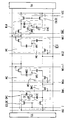
- a bit line BL is shown with its two bit line halves BLH, BLH , to which on one side a sense amplifier SA is connected and on the other side a precharging device EQL for precharging and (with regard to its electrical potential) equating the bit line halves BLH, BLH to a bit line potential VBL before reading data from memory cells MC.
- memory cells MC of the transistor type are shown (with selection transistors MCT and storage capacitors MCC), on the one hand with the respective bit line half BLH, BLH are connected and on the other hand (on the first electrodes of their storage capacitors MCC) all together with a so-called plate potential VPL.
- This has essentially half the value of the difference between the supply voltage potential VDD (or internal supply voltage potential VDDint) and the reference potential VSS. It is therefore essentially equal to the bit line potential VBL, which can be applied to the bit lines BL via the precharging device EQL.
- the plate potential VPL could also essentially have the value of the supply voltage potential VDD (or that of the internal supply voltage potential VDDint) or the reference potential VSS.
- the figure shows word lines WL (numbered from WL1 to WLn) for driving the selection transistors MCT of the memory cells MC.
- the memory cells MC are thus, as is generally customary, arranged at intersections between word lines WL and bit lines BL and, via their selection transistors MCT, for reading and storing information with the respective bit lines BL or bit line halves BLH; BLH connectable.
- Each bit line half BLH, BLH has (for example, arranged at its ends as shown) a so-called dummy cell DMC, which is also of the transistor cell type. As is generally known, this serves to uniformly and symmetrically load the differentially operating sense amplifiers SA during operation.
- the storage capacitors DC of the dummy cells DMC are also connected to the plate potential VPL at their first electrodes.
- marginal cells CMC which are generally referred to as "friendly cells” are called, but they will only be later as they are not described for the present invention are absolutely necessary.
- the previously described semiconductor memory circuit corresponds fully state of the art. According to the invention, this semiconductor memory circuit however, additional devices EQLDC, by means of which the second electrodes of the Storage capacitors DC of the dummy memory cells DMC in operation can be charged with a precharge potential VDC.
- the loading takes place according to the invention during (usual) precharging of the bit lines BL to the bit line potential VBL.
- the value of the precharge potential VDC is 5 to 35% greater than the value of half the difference from the supply voltage potential VDD (or VDDint when using an internal Supply voltage potential) and reference potential VSS.
- the devices EQLDC can, for example, as shown, Transistors contain the one with the precharge potential VDC are connected and on the other hand to the second electrodes of the storage capacitors DC of the dummy cells DMC.
- the transistors are gated by a precharge clock signal T, which at the time of precharging the transistors switch.
- the precharge clock signal T can be the same in time Have a course like a corresponding one (not shown) Clock signal, which is read out of data from the memory cells MC precharging the bit lines BL to their bit line potential VBL controls.
- marginal cells CMC which are generally referred to as "friendly cells” be designated. Their function is known to the expert. she can either consist only of edge cell capacitors CC, as shown here. But you can also go beyond still contain transistors, similar to the selection transistors MCT of memory cells MC or of dummy cells DMC.
- first electrodes of the edge cell capacitors CC with the plate potential VPL connected and the second electrodes of this Edge cell capacitors CC are by means of the equalizers EQLDC for the dummy cells DMC also with the precharge potential VDC of the DMC dummy cells can be applied. This then results in an even better symmetry of the working and Load ratios of the sense amplifier SA when reading out as well as evaluating and amplifying the data read out.
Landscapes
- Engineering & Computer Science (AREA)
- Microelectronics & Electronic Packaging (AREA)
- Computer Hardware Design (AREA)
- Dram (AREA)
- Credit Cards Or The Like (AREA)
Abstract
Description
Die Erfindung betrifft eine integrierte Halbleiterspeicherschaltung
mit den Merkmalen des Oberbegriffes nach Patentanspruch
1 sowie ein Verfahren zum Betreiben derselben. Eine solche Halbleiterspeicherschaltung ist beispielsweise aus EP-A-0 398 245 bekannt.The invention relates to an integrated semiconductor memory circuit
with the features of the preamble according to
Bei integrierten Halbleiterspeicherschaltungen ist es allgemein üblich, vor einem Auslesen von Daten aus den Speicherzellen MC die Bitleitungen BL auf ein Bitleitungspotential VBL vorzuladen (allgemein als Precharge-Vorgang bzw. mit Precharge-Potential bezeichnet). Dies dient dazu, den Leseverstärkern SA (die ja im allgemeinen Flip-Flop-Schaltungen sind, die differenziell arbeiten) nach dem Auslesen zur Bewertung und Verstärkung der Lesesignale effektiv nur diese zuzuführen, weil das Bitleitungspotential VBL an beiden Eingängen der Leseverstärker SA mit dem selben Wert anliegt und somit von den differenziell arbeitenden Leseverstärkern SA nicht berücksichtigt wird. Während in der Vergangenheit als Bitleitungspotential VBL meist entweder das Versorgungspotential VDD oder das Bezugspotential VSS angelegt wurde, legt man heutzutage meist einen Wert an, der der halben Differenz aus Versorgungsspannungspotential VDD und Bezugspotential VSS entspricht bzw. bei solchen Halbleiterspeicherschaltungen, die schaltungsintern mit einem gegenüber dem am fertigen Baustein anliegenden Versorgungspotential VDD erniedrigten sogenannten internen Versorgungsspannungspotential VDDint arbeiten, legt man die entsprechende halbe Differenz zwischen diesem internen Versorgungsspannungspotential VDDint und dem Bezugspotential VSS an. It is general with integrated semiconductor memory circuits usual, before reading data from the memory cells MC precharge the bit lines BL to a bit line potential VBL (generally as a pre-charge process or with pre-charge potential designated). This serves the sense amplifiers SA (which yes in the general flip-flop circuits that are differential work) after reading for evaluation and reinforcement of the Read signals effectively feed these only because of the bitline potential VBL at both inputs of the sense amplifier SA with the same value and therefore different from the working sense amplifiers SA is not taken into account. While in the past mostly as bit line potential VBL either the supply potential VDD or the reference potential VSS was created, you usually create a value these days, that is half the difference from the supply voltage potential VDD and reference potential corresponds to VSS or in such semiconductor memory circuits, the internal circuit with one opposite the supply potential VDD applied to the finished module reduced so-called internal supply voltage potential VDDint work, you put the corresponding half difference between this internal supply voltage potential VDDint and the reference potential VSS.
Soweit die herkömmliche Halbleiterspeicherschaltung auch sogenannte Dummy-Zellen aufweist, werden herkömmlicherweise auch diese auf das Bitleitungspotential VBL aufgeladen.As far as the conventional semiconductor memory circuit also so-called Dummy cells are also commonly used these are charged to the bit line potential VBL.
Bekanntlich sind integrierte Halbleiterspeicherschaltungen, insbesondere vom lTransistor-Speicherzellentyp (sogenannte 1T-DRAM's bzw. embedded 1T-DRAM's), empfindlich gegenüber sogenannten Soft-Errors, d.h. gegenüber Alphastrahlen, die meist vom verwendeten Bausteingehäuse herrühren. Versuche haben gezeigt, daß die herkömmlichen Halbleiterspeicherschaltungen unterschiedlich stark auf diese Alphastrahlen reagieren, je nachdem, ob ein Datum als physikalische 0 oder als physikalische 1 zu speichern war (eine physikalische 0 kann einem Datum log. 0 entsprechen; sie kann aber auch einem Datum log. 1 entsprechen; die Zuordnung ist abhängig von der jeweils gewählten Schaltungstechnik). Es hat sich gezeigt, daß dies Folge einer sogenannten Bewertungsunsymmetrie der Leseverstärker SA ist, so daß z.B. ein gespeichertes Datum phys. 0 nicht mit derselben Sicherheit und denselben Sicherheitsmargins auslesbar ist wie ein gespeichertes Datum phys. 1 und umgekehrt. Damit jedoch nimmt die Gefahr des Auftretens von Soft-Errors bezüglich der einen Datumsart zu, während sie gegenüber der anderen Datumsart abnimmt. Dies ist insoweit unerwünscht, weil man gern für beide Datumsarten eine gleich gute Sicherheit gegenüber Soft-Errors haben will.Integrated semiconductor memory circuits are known in particular of the transistor memory cell type (so-called 1T DRAMs or embedded 1T-DRAM's), sensitive to so-called Soft errors, i.e. against alpha rays, the most derive from the block housing used. Have attempts shown that the conventional semiconductor memory circuits react differently to these alpha rays, each after whether a date as physical 0 or as physical 1 was saved (a physical 0 can be a date log. Correspond to 0; but it can also log a date. 1 correspond; the assignment depends on the selected one Circuit technology). It has been shown that this is the result of a so-called evaluation asymmetry of the sense amplifier SA, so that e.g. a stored date phys. 0 not with the same Security and the same security margin can be read as a saved date phys. 1 and vice versa. But with that takes the risk of the occurrence of soft errors regarding the one date type while opposing the other date type decreases. This is undesirable because you like to do both Date types provide equally good security against soft errors wants.
Als Ausweg böte sich an, die Speicherzellenkapazitäten zu vergrößern, wodurch das Lesesignal größer würde und die Halbleiterspeicherschaltung somit insgesamt sicherer gegenüber Soft-Errors. Allerdings ist dieser Weg in der Praxis nicht gangbar, weil dies eine laterale und/oder räumliche Vergrößerung der Speicherzellen zur Folge hätte, was bei den heute bestehenden Anforderungen an Miniaturisierung von Halbleiterspeicherschaltungen nicht gewünscht ist (die Folge wären größere Speicherchips und ggf. dazu notwendige größere Gehäuse, die dann unter Umständen nicht mehr den geltenden Normen entsprechen).The way out would be to increase the memory cell capacities, whereby the read signal would be larger and the semiconductor memory circuit overall more secure against soft errors. However, this path is not feasible in practice, because this is a lateral and / or spatial enlargement of the Memory cells would result in what with the existing today Miniaturization requirements for semiconductor memory circuits is not desired (the result would be larger memory chips and if necessary, larger housing, which is then under May no longer meet the applicable standards).
Aufgabe der vorliegenden Erfindung ist es, gattungsgemäße integrierte Halbleiterspeicherschaltungen so zu optimieren, daß ihre Leseverstärker die Daten phys. 0 und phys. 1 mit annähernd gleicher Sicherheit erkennen können (sog. Symmetrierung der Leseverstärker bezüglich phys. 0 und phys. 1), ohne dazu die Speicherzellen vergrößern zu müssen und ohne dabei eine Einbuße an Sicherheit gegenüber Soft-Errors in Kauf nehmen zu müssen. Aufgabe ist es auch, ein entsprechendes Betriebsverfahren für eine solche Halbleiterspeicherschaltung anzugeben.The object of the present invention is to generic integrated To optimize semiconductor memory circuits so that their sense amplifiers the data phys. 0 and phys. 1 with approximately can recognize the same security (so-called symmetrization of the Sense amplifier with respect to phys. 0 and phys. 1), without the Having to enlarge memory cells and without sacrificing anything to have to accept security against soft errors. It is also the task to develop an appropriate operating procedure for to specify such a semiconductor memory circuit.
Diese Aufgabe wird gelöst durch die kennzeichnenden Merkmale
der Patentansprüche 1 und 3. Vorteilhafte Weiterbildungen sind
in Unteransprüchen gekennzeichnet.This problem is solved by the characteristic features
of
Die vorliegende Erfindung ermöglicht es, die Soft-Error-Rate um zwei Größenordnungen zu senken im Vergleich zu den bekannten, gattungsgemäßen Halbleiterspeicherschaltungen.The present invention enables the soft error rate to be changed lower two orders of magnitude compared to the known, Generic semiconductor memory circuits.
Nachstehend wird die Erfindung anhand einer Figur erläutert, welche auch vorteilhafte Weiterbildungen enthält.The invention is explained below with reference to a figure, which also contains advantageous developments.
Die Figur zeigt einen Ausschnitt aus einer erfindungsgemäßen
Halbleiterspeicherschaltung, bei der aus Gründen der Übersichtlichkeit
nur für die Erfindung wesentliches dargestellt wurde.
Gezeigt ist eine Bitleitung BL mit ihren beiden Bitleitungshälften
BLH,
Weiterhin zeigt die Figur Wortleitungen WL (durchnummeriert von
WL1 bis WLn) zur Ansteuerung der Auswahltransistoren MCT der
Speicherzellen MC. Die Speicherzellen MC sind also, wie allgemein
üblich, an Kreuzungspunkten zwischen Wort leitungen WL und
Bitleitungen BL angeordnet und über ihre Auswahltransistoren
MCT zum Lesen und Speichern von Informationen mit den jeweiligen
Bitleitungen BL bzw. Bitleitungshälften BLH;
Jede Bitleitungshälfte BLH,
Zwar zeigt die Figur noch Randzellen CMC, die allgemein als "friendly cells" bezeichnet werden, doch werden diese erst später beschrieben, da sie für die vorliegende Erfindung nicht unbedingt notwendig sind.The figure still shows marginal cells CMC, which are generally referred to as "friendly cells" are called, but they will only be later as they are not described for the present invention are absolutely necessary.
Die bislang geschilderte Halbleiterspeicherschaltung entspricht voll dem Stand der Technik. Erfindungsgemäß weist diese Halbleiterspeicherschaltung jedoch noch zusätzlich Vorrichtungen EQLDC auf, mittels deren die jeweils zweiten Elektroden der Speicherkondensatoren DC der Dummyspeicherzellen DMC im Betrieb mit einem Vorladepotential VDC beaufschlagbar sind. Das Beaufschlagen erfolgt erfindungsgemäß während des (üblichen) Vorladens der Bitleitungen BL auf das Bitleitungspotential VBL. Der Wert des Vorladepotentials VDC ist erfindungsgemäß 5 bis 35% größer als der Wert der halben Differenz aus Versorgungsspannungspotential VDD (bzw. VDDint bei Verwendung eines internen Versorgungsspannungspotentials) und Bezugspotential VSS.The previously described semiconductor memory circuit corresponds fully state of the art. According to the invention, this semiconductor memory circuit however, additional devices EQLDC, by means of which the second electrodes of the Storage capacitors DC of the dummy memory cells DMC in operation can be charged with a precharge potential VDC. The loading takes place according to the invention during (usual) precharging of the bit lines BL to the bit line potential VBL. Of the According to the invention, the value of the precharge potential VDC is 5 to 35% greater than the value of half the difference from the supply voltage potential VDD (or VDDint when using an internal Supply voltage potential) and reference potential VSS.
Die Vorrichtungen EQLDC können beispielsweise, wie dargestellt, Transistoren enthalten, die einerseits mit dem Vorladepotential VDC verbunden sind und andererseits mit den zweiten Elektroden der Speicherkondensatoren DC der Dummy-Zellen DMC. Die Transistoren sind gatemäßig von einem Vorladetaktsignal T angesteuert, welche im Zeitpunkt des Vorladens die Transistoren leitend schalten. Das Vorladetaktsignal T kann denselben zeitlichen Verlauf aufweisen wie ein entsprechendes (nicht dargestelltes) Taktsignal, welches vor einem Auslesen von Daten aus den Speicherzellen MC das Vorladen der Bitleitungen BL auf ihr Bitleitungspotential VBL steuert.The devices EQLDC can, for example, as shown, Transistors contain the one with the precharge potential VDC are connected and on the other hand to the second electrodes of the storage capacitors DC of the dummy cells DMC. The transistors are gated by a precharge clock signal T, which at the time of precharging the transistors switch. The precharge clock signal T can be the same in time Have a course like a corresponding one (not shown) Clock signal, which is read out of data from the memory cells MC precharging the bit lines BL to their bit line potential VBL controls.
Die Figur zeigt auch, wie bereits erwähnt, das Vorhandensein von Randzellen CMC, welche im allgemeinen als "friendly cells" bezeichnet werden. Ihre Funktion ist dem Fachmann bekannt. Sie können entweder lediglich aus Randzellenkondensatoren CC bestehen, wie hier dargestellt. Sie können aber auch darüber hinaus noch Transistoren enthalten, ähnlich den Auswahltransistoren MCT von Speicherzellen MC oder denen von Dummy-Zellen DMC. In vorteilhafter Weise sind bei der vorliegenden Erfindung die ersten Elektroden der Randzellenkondensatoren CC mit dem Plattenpotential VPL verbunden und die zweiten Elektroden dieser Randzellenkondensatoren CC sind mittels der Ausgleichsvorrichtungen EQLDC für die Dummy-Zellen DMC ebenfalls mit dem Vorladepotential VDC der Dummy-Zellen DMC beaufschlagbar. Dies ergibt dann eine noch bessere Symmetriesierung der Arbeits- und Belastungsverhältnisse der Leseverstärker SA beim Auslesen sowie Bewerten und Verstärken der ausgelesenen Daten.As already mentioned, the figure also shows the presence of marginal cells CMC, which are generally referred to as "friendly cells" be designated. Their function is known to the expert. she can either consist only of edge cell capacitors CC, as shown here. But you can also go beyond still contain transistors, similar to the selection transistors MCT of memory cells MC or of dummy cells DMC. In are advantageous in the present invention first electrodes of the edge cell capacitors CC with the plate potential VPL connected and the second electrodes of this Edge cell capacitors CC are by means of the equalizers EQLDC for the dummy cells DMC also with the precharge potential VDC of the DMC dummy cells can be applied. This then results in an even better symmetry of the working and Load ratios of the sense amplifier SA when reading out as well as evaluating and amplifying the data read out.
Claims (4)
- Integrated semiconductor memory circuithaving apparatuses (EQLDC) by means of which a precharge potential (VDC) can be applied in each case to second electrodes of the storage capacitors (DC) of the dummy memory cells (DMC) during operation,having a supply voltage potential and having a reference-earth potential,having memory cells (MC) of the 1-Transistor type which each contain a selection transistor and at least one storage capacitor (MCC) and are arranged in matrix form at points where wordlines (WL; WL1...WLn) cross bit lines (BL),each bit line (BL) being formed from two bit line halves (BLH;
BLH ) and, during operation, being charged to half the difference between supply potential and reference-earth potential, andeach memory cell (MC), on the one hand, being connected via its selection transistor to a respective bit line half (BLH;BLH ), and, on the other hand, a first electrode of the at least one storage capacitor (MCC) being connected, during operation, to a plate potential (VPL) of a predetermined value,having at least one dummy memory cell (DMC), likewise containing at least one storage capacitor (DC), per bit line half (BLH;BLH ), a first electrode of the at least one storage capacitor (DC) likewise being connected to the plate potential (VPL) during operation,
characterized in that the precharge potential has a value which is 5 to 35% greater than the value of half the difference between supply voltage potential and reference-earth potential. - Integrated semiconductor memory circuit according to Claim 1, having at least one edge cell (CMC) per bit line half (BLH;
BLH ), which contains at least one edge cell capacitor (CC) whose first electrode is connected to the plate potential (VPL),
characterized
in that
the precharge potential (VDC) can be applied to the second electrode of the edge cell capacitor (CC). - Method for operating an integrated semiconductor memory circuit having the features of Claims 1 or 2, in which prior to a read-out of data stored in memory cells (MC), the bit lines (BL) are precharged to a bit line potential (VBL),
the precharge potential (VDC) being applied to the second electrodes of the storage capacitors (DC) of the dummy memory cells (DMC) during the precharging of the bit lines (BL). - Method according to Claim 3,
the precharge potential (VDC) also being applied to the second electrodes of the edge cell capacitors (CC) during the precharging of the bit lines (BL).
Applications Claiming Priority (2)
| Application Number | Priority Date | Filing Date | Title |
|---|---|---|---|
| DE4400699 | 1994-01-12 | ||
| DE4400699 | 1994-01-12 |
Publications (3)
| Publication Number | Publication Date |
|---|---|
| EP0663667A2 EP0663667A2 (en) | 1995-07-19 |
| EP0663667A3 EP0663667A3 (en) | 1995-10-25 |
| EP0663667B1 true EP0663667B1 (en) | 1999-03-03 |
Family
ID=6507778
Family Applications (1)
| Application Number | Title | Priority Date | Filing Date |
|---|---|---|---|
| EP94120451A Expired - Lifetime EP0663667B1 (en) | 1994-01-12 | 1994-12-22 | Integrated semiconductor memory circuit and operation thereof |
Country Status (7)
| Country | Link |
|---|---|
| US (1) | US5574694A (en) |
| EP (1) | EP0663667B1 (en) |
| JP (1) | JP3857330B2 (en) |
| KR (1) | KR100383291B1 (en) |
| AT (1) | ATE177246T1 (en) |
| DE (1) | DE59407879D1 (en) |
| HK (1) | HK1004240A1 (en) |
Families Citing this family (6)
| Publication number | Priority date | Publication date | Assignee | Title |
|---|---|---|---|---|
| DE19503782A1 (en) * | 1995-02-04 | 1996-08-08 | Philips Patentverwaltung | Delay circuit |
| JP3824370B2 (en) * | 1997-03-03 | 2006-09-20 | 富士通株式会社 | Semiconductor device |
| KR100908699B1 (en) * | 2002-09-13 | 2009-07-22 | 주식회사 포스코 | Wastewater Treatment System of Oil Separation Tank |
| JP4084149B2 (en) * | 2002-09-13 | 2008-04-30 | 富士通株式会社 | Semiconductor memory device |
| JP5700907B2 (en) * | 2008-06-26 | 2015-04-15 | ピーエスフォー ルクスコ エスエイアールエルPS4 Luxco S.a.r.l. | Semiconductor memory device |
| US20100269845A1 (en) * | 2009-04-23 | 2010-10-28 | Bernhard Peter Tamme | Hair styling device & methods of use thereof |
Family Cites Families (10)
| Publication number | Priority date | Publication date | Assignee | Title |
|---|---|---|---|---|
| GB1523752A (en) * | 1974-08-28 | 1978-09-06 | Siemens Ag | Dynamic semiconductor data stores |
| US4658382A (en) * | 1984-07-11 | 1987-04-14 | Texas Instruments Incorporated | Dynamic memory with improved dummy cell circuitry |
| US4598389A (en) * | 1984-10-01 | 1986-07-01 | Texas Instruments Incorporated | Single-ended CMOS sense amplifier |
| JPS6282597A (en) * | 1985-10-08 | 1987-04-16 | Fujitsu Ltd | Semiconductor storage device |
| JPS63282993A (en) * | 1987-05-15 | 1988-11-18 | Mitsubishi Electric Corp | Semiconductor dynamic random access memory |
| US5255235A (en) * | 1987-05-15 | 1993-10-19 | Mitsubishi Denki Kabushiki Kaisha | Dynamic random access memory with dummy word lines connected to bit line potential adjusting capacitors |
| JPH01119984A (en) * | 1987-10-31 | 1989-05-12 | Toshiba Corp | Dynamic type semiconductor memory |
| JPH0762955B2 (en) * | 1989-05-15 | 1995-07-05 | 株式会社東芝 | Dynamic random access memory |
| US5301157A (en) * | 1992-06-01 | 1994-04-05 | Micron Technology, Inc. | Coupling circuit and method for discharging a non-selected bit line during accessing of a memory storage cell |
| US5291437A (en) * | 1992-06-25 | 1994-03-01 | Texas Instruments Incorporated | Shared dummy cell |
-
1994
- 1994-12-22 DE DE59407879T patent/DE59407879D1/en not_active Expired - Fee Related
- 1994-12-22 AT AT94120451T patent/ATE177246T1/en not_active IP Right Cessation
- 1994-12-22 EP EP94120451A patent/EP0663667B1/en not_active Expired - Lifetime
-
1995
- 1995-01-05 KR KR1019950000072A patent/KR100383291B1/en not_active IP Right Cessation
- 1995-01-09 JP JP01749695A patent/JP3857330B2/en not_active Expired - Fee Related
- 1995-01-12 US US08/371,827 patent/US5574694A/en not_active Expired - Fee Related
-
1998
- 1998-04-20 HK HK98103298A patent/HK1004240A1/en not_active IP Right Cessation
Also Published As
| Publication number | Publication date |
|---|---|
| HK1004240A1 (en) | 1998-11-20 |
| KR100383291B1 (en) | 2003-06-25 |
| US5574694A (en) | 1996-11-12 |
| ATE177246T1 (en) | 1999-03-15 |
| JP3857330B2 (en) | 2006-12-13 |
| JPH07235179A (en) | 1995-09-05 |
| DE59407879D1 (en) | 1999-04-08 |
| KR950033216A (en) | 1995-12-22 |
| EP0663667A3 (en) | 1995-10-25 |
| EP0663667A2 (en) | 1995-07-19 |
Similar Documents
| Publication | Publication Date | Title |
|---|---|---|
| EP1118081B1 (en) | Integrated memory with differential read amplifier | |
| DE4024295C2 (en) | Dynamic semiconductor memory device | |
| DE4003673C2 (en) | ||
| DE19756929B4 (en) | Cell array and sense amplifier structure with improved noise characteristics and reduced size | |
| DE60107174T2 (en) | A semiconductor memory device | |
| EP0991079B1 (en) | Integrated memory | |
| EP0663667B1 (en) | Integrated semiconductor memory circuit and operation thereof | |
| DE10154613B4 (en) | Method for precharging memory cells of a dynamic semiconductor memory during power up and semiconductor memory | |
| EP0663666B1 (en) | Integrated semiconductor memory circuit and operation thereof | |
| DE19952311B4 (en) | Integrated memory with memory cells of 2-transistor / 2-capacitor type | |
| EP1163677B1 (en) | Integrated memory with memory cells and reference cells and corresponding operating method | |
| EP1102168B1 (en) | Integrated memory with memory cells and reference cells | |
| DE19647135A1 (en) | Ultra-high integrated DRAM | |
| DE19903198C1 (en) | Integrated semiconductor memory device e.g. DRAM | |
| EP0967616B1 (en) | Integrated memory | |
| EP0732703B1 (en) | Method for testing a semiconductor memory circuit | |
| EP1166276B1 (en) | Integrated ferroelectric memory whose plate lines are selected by a column decoder | |
| EP0897181B1 (en) | Circuit for processing memory cell data | |
| DE10392198T5 (en) | Increase a refresh period in a semiconductor memory device | |
| DE10315087B3 (en) | Dynamic memory cell refreshing method for memory circuit for mobile applications effected with minimum current requirement | |
| DE4231169C2 (en) | Semiconductor memory device and method for operating such a device | |
| DE19913108A1 (en) | Integrated memory with memory cells and reference cells as well as operating methods for such a memory | |
| DE10017368B4 (en) | Method for operating an integrated memory | |
| DE19913570C2 (en) | Operating methods for an integrated memory and integrated memory | |
| DE3826418A1 (en) | Read amplifier |
Legal Events
| Date | Code | Title | Description |
|---|---|---|---|
| PUAI | Public reference made under article 153(3) epc to a published international application that has entered the european phase |
Free format text: ORIGINAL CODE: 0009012 |
|
| AK | Designated contracting states |
Kind code of ref document: A2 Designated state(s): AT DE FR GB IE IT NL |
|
| PUAL | Search report despatched |
Free format text: ORIGINAL CODE: 0009013 |
|
| AK | Designated contracting states |
Kind code of ref document: A3 Designated state(s): AT DE FR GB IE IT NL |
|
| 17P | Request for examination filed |
Effective date: 19960419 |
|
| GRAG | Despatch of communication of intention to grant |
Free format text: ORIGINAL CODE: EPIDOS AGRA |
|
| GRAG | Despatch of communication of intention to grant |
Free format text: ORIGINAL CODE: EPIDOS AGRA |
|
| GRAH | Despatch of communication of intention to grant a patent |
Free format text: ORIGINAL CODE: EPIDOS IGRA |
|
| 17Q | First examination report despatched |
Effective date: 19980706 |
|
| GRAH | Despatch of communication of intention to grant a patent |
Free format text: ORIGINAL CODE: EPIDOS IGRA |
|
| GRAA | (expected) grant |
Free format text: ORIGINAL CODE: 0009210 |
|
| AK | Designated contracting states |
Kind code of ref document: B1 Designated state(s): AT DE FR GB IE IT NL |
|
| REF | Corresponds to: |
Ref document number: 177246 Country of ref document: AT Date of ref document: 19990315 Kind code of ref document: T |
|
| REG | Reference to a national code |
Ref country code: IE Ref legal event code: FG4D Free format text: GERMAN |
|
| REF | Corresponds to: |
Ref document number: 59407879 Country of ref document: DE Date of ref document: 19990408 |
|
| ET | Fr: translation filed | ||
| ITF | It: translation for a ep patent filed |
Owner name: STUDIO JAUMANN P. & C. S.N.C. |
|
| GBT | Gb: translation of ep patent filed (gb section 77(6)(a)/1977) |
Effective date: 19990506 |
|
| PLBE | No opposition filed within time limit |
Free format text: ORIGINAL CODE: 0009261 |
|
| STAA | Information on the status of an ep patent application or granted ep patent |
Free format text: STATUS: NO OPPOSITION FILED WITHIN TIME LIMIT |
|
| 26N | No opposition filed | ||
| REG | Reference to a national code |
Ref country code: GB Ref legal event code: IF02 |
|
| PGFP | Annual fee paid to national office [announced via postgrant information from national office to epo] |
Ref country code: NL Payment date: 20051214 Year of fee payment: 12 |
|
| PGFP | Annual fee paid to national office [announced via postgrant information from national office to epo] |
Ref country code: AT Payment date: 20051220 Year of fee payment: 12 |
|
| PGFP | Annual fee paid to national office [announced via postgrant information from national office to epo] |
Ref country code: GB Payment date: 20061221 Year of fee payment: 13 |
|
| PG25 | Lapsed in a contracting state [announced via postgrant information from national office to epo] |
Ref country code: NL Free format text: LAPSE BECAUSE OF NON-PAYMENT OF DUE FEES Effective date: 20070701 |
|
| NLV4 | Nl: lapsed or anulled due to non-payment of the annual fee |
Effective date: 20070701 |
|
| PG25 | Lapsed in a contracting state [announced via postgrant information from national office to epo] |
Ref country code: AT Free format text: LAPSE BECAUSE OF NON-PAYMENT OF DUE FEES Effective date: 20061222 |
|
| PGFP | Annual fee paid to national office [announced via postgrant information from national office to epo] |
Ref country code: IT Payment date: 20071222 Year of fee payment: 14 |
|
| PGFP | Annual fee paid to national office [announced via postgrant information from national office to epo] |
Ref country code: DE Payment date: 20080213 Year of fee payment: 14 |
|
| PGFP | Annual fee paid to national office [announced via postgrant information from national office to epo] |
Ref country code: FR Payment date: 20071217 Year of fee payment: 14 |
|
| GBPC | Gb: european patent ceased through non-payment of renewal fee |
Effective date: 20071222 |
|
| PG25 | Lapsed in a contracting state [announced via postgrant information from national office to epo] |
Ref country code: GB Free format text: LAPSE BECAUSE OF NON-PAYMENT OF DUE FEES Effective date: 20071222 |
|
| PGFP | Annual fee paid to national office [announced via postgrant information from national office to epo] |
Ref country code: IE Payment date: 20071220 Year of fee payment: 14 |
|
| REG | Reference to a national code |
Ref country code: IE Ref legal event code: MM4A |
|
| REG | Reference to a national code |
Ref country code: FR Ref legal event code: ST Effective date: 20090831 |
|
| PG25 | Lapsed in a contracting state [announced via postgrant information from national office to epo] |
Ref country code: IE Free format text: LAPSE BECAUSE OF NON-PAYMENT OF DUE FEES Effective date: 20081222 Ref country code: DE Free format text: LAPSE BECAUSE OF NON-PAYMENT OF DUE FEES Effective date: 20090701 |
|
| PG25 | Lapsed in a contracting state [announced via postgrant information from national office to epo] |
Ref country code: FR Free format text: LAPSE BECAUSE OF NON-PAYMENT OF DUE FEES Effective date: 20081231 |
|
| PG25 | Lapsed in a contracting state [announced via postgrant information from national office to epo] |
Ref country code: IT Free format text: LAPSE BECAUSE OF NON-PAYMENT OF DUE FEES Effective date: 20081222 |