EP0652413A2 - Signal transmission system for trigger probe - Google Patents
Signal transmission system for trigger probe Download PDFInfo
- Publication number
- EP0652413A2 EP0652413A2 EP95200123A EP95200123A EP0652413A2 EP 0652413 A2 EP0652413 A2 EP 0652413A2 EP 95200123 A EP95200123 A EP 95200123A EP 95200123 A EP95200123 A EP 95200123A EP 0652413 A2 EP0652413 A2 EP 0652413A2
- Authority
- EP
- European Patent Office
- Prior art keywords
- signal
- probe
- transmitter
- receiver
- time
- Prior art date
- Legal status (The legal status is an assumption and is not a legal conclusion. Google has not performed a legal analysis and makes no representation as to the accuracy of the status listed.)
- Granted
Links
Images


Classifications
-
- G—PHYSICS
- G01—MEASURING; TESTING
- G01B—MEASURING LENGTH, THICKNESS OR SIMILAR LINEAR DIMENSIONS; MEASURING ANGLES; MEASURING AREAS; MEASURING IRREGULARITIES OF SURFACES OR CONTOURS
- G01B21/00—Measuring arrangements or details thereof, where the measuring technique is not covered by the other groups of this subclass, unspecified or not relevant
- G01B21/02—Measuring arrangements or details thereof, where the measuring technique is not covered by the other groups of this subclass, unspecified or not relevant for measuring length, width, or thickness
- G01B21/04—Measuring arrangements or details thereof, where the measuring technique is not covered by the other groups of this subclass, unspecified or not relevant for measuring length, width, or thickness by measuring coordinates of points
- G01B21/047—Accessories, e.g. for positioning, for tool-setting, for measuring probes
-
- G—PHYSICS
- G01—MEASURING; TESTING
- G01B—MEASURING LENGTH, THICKNESS OR SIMILAR LINEAR DIMENSIONS; MEASURING ANGLES; MEASURING AREAS; MEASURING IRREGULARITIES OF SURFACES OR CONTOURS
- G01B5/00—Measuring arrangements characterised by the use of mechanical techniques
- G01B5/004—Measuring arrangements characterised by the use of mechanical techniques for measuring coordinates of points
- G01B5/008—Measuring arrangements characterised by the use of mechanical techniques for measuring coordinates of points using coordinate measuring machines
- G01B5/012—Contact-making feeler heads therefor
-
- G—PHYSICS
- G01—MEASURING; TESTING
- G01B—MEASURING LENGTH, THICKNESS OR SIMILAR LINEAR DIMENSIONS; MEASURING ANGLES; MEASURING AREAS; MEASURING IRREGULARITIES OF SURFACES OR CONTOURS
- G01B7/00—Measuring arrangements characterised by the use of electric or magnetic techniques
- G01B7/002—Constructional details of contacts for gauges actuating one or more contacts
-
- G—PHYSICS
- G01—MEASURING; TESTING
- G01B—MEASURING LENGTH, THICKNESS OR SIMILAR LINEAR DIMENSIONS; MEASURING ANGLES; MEASURING AREAS; MEASURING IRREGULARITIES OF SURFACES OR CONTOURS
- G01B7/00—Measuring arrangements characterised by the use of electric or magnetic techniques
- G01B7/004—Measuring arrangements characterised by the use of electric or magnetic techniques for measuring coordinates of points
- G01B7/008—Measuring arrangements characterised by the use of electric or magnetic techniques for measuring coordinates of points using coordinate measuring machines
- G01B7/012—Contact-making feeler heads therefor
-
- G—PHYSICS
- G01—MEASURING; TESTING
- G01B—MEASURING LENGTH, THICKNESS OR SIMILAR LINEAR DIMENSIONS; MEASURING ANGLES; MEASURING AREAS; MEASURING IRREGULARITIES OF SURFACES OR CONTOURS
- G01B2210/00—Aspects not specifically covered by any group under G01B, e.g. of wheel alignment, caliper-like sensors
- G01B2210/58—Wireless transmission of information between a sensor or probe and a control or evaluation unit
Definitions
- This invention relates to probes for use on machines which determine a position of a workpiece, such as coordinate measuring machines and machine tools. More particularly, it relates to signal transmission systems for such probes.
- a trigger probe for such purposes is described in US patent 4,153,998 (McMurtry).
- the probe In use, the probe is moved by the machine relative to a workpiece.
- the probe has a deflectable stylus, and delivers a trigger signal when the stylus contacts the workpiece.
- the trigger signal is indicated by the probe switching from one state to another.
- the trigger signal is used by the control of the machine to freeze the outputs of scales or other measuring means which indicate the position of the probe. The position of the point of contact on the workpiece surface can thus be determined.
- the accuracy would be destroyed if the signal transmission system were not repeatable, that is, if there were an unknown, variable delay in the signal transmission. If this occurs, then the probe will travel an unknown, variable distance after the instant of generation of the trigger signal before the machine control is able to freeze the outputs of the measuring means. There is then an error between the position of contact and the position indicated by the frozen outputs, and this error is an unknown, variable quantity which cannot be removed by calibration.
- the probe calibration procedure mentioned above will then also remove this repeatable delay caused by the transmission system.
- One commercially available radio probe transmission system for example, used a frequency shift keying method. Modulated onto the radio frequency carrier is one of two possible audio signals, having two different frequencies representing the two possible states of the probe.
- the trigger signal is indicated by a change of the audio signal from one frequency to the other when the probe changes state.
- the receiver of this system has difficulty in detecting the trigger signal in a repeatable manner, since the minimum time required to recognise the change from one audio frequency to the other is one cycle of the audio frequency, and probably two cycles. It is impossible for the receiver to know at what time during the previous cycle the change of state in the probe occurred.
- the uncertainty in the detection of the trigger signal therefore, is at least one quarter of a cycle of the audio signal, giving rise to a corresponding degree of non-repeatability. If the audio frequency is increased to reduce this problem, the bandwidth would also be increased.
- One aspect of the present invention provides a signal transmission system for a probe for a position determination machine, comprising a transmitter for mounting with the probe, and a receiver for mounting on the machine for receiving the signal transmitted by the transmitter, and including: master reference means in the transmitter for producing a master reference signal having a reference frequency; slave reference means in the receiver for producing a slave reference signal which is synchronised with respect to said reference frequency; carrier signal generating means in the transmitter for producing a carrier signal which is synchronised with respect to said reference frequency; means in the transmitter for modulating a probe signal onto said carrier signal; means in the receiver for receiving said modulated carrier signal; and means in the receiver for demodulating said probe signal from said modulated carrier signal, synchronously with the slave reference signal.
- the modulating means is a phase modulating means for modulating the probe signal onto the carrier signal.
- the signal transmission system has a separate reference signal for keeping synchronism between the transmitter and the receiver, it is possible to detect the switching between one state of the probe output and the other state thereof more quickly and reliably than in the above mentioned commercially available radio transmission system.
- the receiver can thus determine the current state of the probe output even after such interference.
- such a system can be realised with a relatively low bandwidth, if desired for a radio transmission system.
- a second aspect of the present invention provides a signal transmission system for a probe for a position determination machine, comprising a transmitter for mounting with the probe, and a receiver for mounting on the machine for receiving the signal transmitted by the transmitter, and including: carrier signal generating means in the transmitter for producing a carrier signal for transmission to the receiver; means in the transmitter for modulating a probe signal onto the carrier signal; timer means in the transmitter for determining the time of occurrence of a probe signal; means for transmitting data representing the time determined by the timer means; and means in the receiver for receiving said data representing the time and producing a probing output signal derived therefrom.
- this enables the modulation of the carrier to change state at a defined transition point in the carrier cycle, while still passing time information as to whereabouts within the carrier cycle the probing signal occurred. It is possible to transmit the time information without greatly increasing the bandwidth of the signal.
- a touch trigger probe 10 constructed in accordance with US patent 4,153,998 includes kinematically arranged seating elements forming electrical contacts 11. Although only one set of electrical contacts 11 is shown, it will be appreciated that there are three such sets, connected in series in a normally closed circuit, which is opened when a deflectable stylus 12 of the probe 10 contacts a workpiece. The opening and closing of these contacts is detected by a status logic circuit 13, which provides debouncing and controls an electronic switch 14.
- a voltage controlled oscillator 16 produces a square wave output which is nominally 1 kHz. This is shown as waveform A in Fig 3, and is used as a carrier signal.
- the precise frequency of the oscillator 16 depends upon the battery voltage VB of the probe 10, enabling information to be transmitted to the receiver of the signal transmission system about the condition of the battery.
- the frequency shift in the oscillator 16 may be, for example, 100 Hz for the full range of possible battery voltage which is to be monitored, e.g. 2 volts.
- the output of the oscillator 16 is fed to a divider 18, which divides it by 2, giving a 500 Hz output which has a definite phase relationship to the 1 kHz signal, shown as waveform B in Fig 3.
- the 1 kHz carrier signal from the oscillator 16 and the 500 Hz signal from the divider 18 are each filtered by respective band pass filters 20,22, giving sinusoidal outputs which are mixed together in a mixer 24.
- the resulting signal is fed to a conventional FM transmitter circuit 26, where it is modulated onto a radio frequency carrier wave and transmitted as a radio signal from an aerial 32 in the probe 10.
- the narrow filters 20,22 limit the bandwidth of the radio signal, to comply with official regulations and to prevent the transmitter from interfering with other nearby equipment.
- the filters 20,22 are digital tracking filters, which have control inputs from the battery voltage VB to shift the sampling frequency.
- the centre frequencies of the pass bands of these filters therefore follow the drift of the oscillator 16 due to battery voltage change.
- the output of the 1 kHz filter 20 is fed to the mixer 24 either directly, or via an inverter 28, under the control of the electronic switch 14.
- the 1 kHz frequency is phase-shifted by 180°.
- a low pass filter 30 is provided at the output of the electronic switch 14, in order to limit the rise time of the data signal which results when the probe contacts 11 change state. Again, this is to limit the bandwidth of the transmitted signal.
- Waveform C in Fig 3 represents the resulting signal at the output of the electronic switch 14, assuming that the signal D is produced from the contacts 11.
- Waveform C is shown in an idealised form, taking no account of the filters 20,30). It will be seen that there is a 180° change of phase at points P and R, corresponding to the instants at which the probe contacts 11 open and close respectively, when a workpiece is probed by the stylus 12 and when the stylus 12 subsequently reseats as it is moved out of contact with the workpiece.
- the filters 20,30 could be replaced by a single low pass filter, placed in the position of the filter 30.
- a filter would have a pass band determined by the necessary bandwidth for the data signal from the contacts 11.
- the signal from the contact 11 will be relatively fast.
- the signal transmitted from the aerial 32 in the transmitter is received by an aerial 34 of a receiver circuit shown in Fig 2, which is mounted at a convenient fixed location on the machine to which the probe 10 is fitted.
- the radio signal is demodulated by an FM detector 36, which suitably may use the signal strength of the radio carrier frequency received to tune accurately the local oscillator within the FM detector 36 for best reception.
- the detector 36 thus delivers an audio signal containing the code shown in waveform C of Fig 3.
- a low pass filter 38 separates out the 500Hz signal and sends it to a battery voltage monitor circuit 40. This circuit provides an output signal when the battery voltage is getting low, to warn the operator of the machine that the probe battery should be changed.
- a high pass filter 42 separates out the 1 kHz signal from the audio output of the detector 36.
- the outputs of the two filters 38,42 are squared up, and taken to a decoder 44.
- the decoder 44 includes a 1 kHz voltage controlled oscillator 46, the output of which is divided by 2 in a divider 48 and then compared with the 500Hz signal from the filter 38 in a phase comparator 50. The result is fed back to the control input of the oscillator 46 thus forming a phase locked loop.
- the oscillator 46 thus recreates the original 1kHz signal produced by the oscillator 16 in the transmitter, shown as waveform A in Fig 3. This is compared with the output of the high pass filter 42 in a phase comparator 52.
- the resulting phase comparison signal contains the information from the probe contacts 11.
- the output from the phase comparator 52 is shown as waveform E in Fig 3. It can be seen that the base line of this signal is zero when the probe contacts are closed, and 1 when the probe contacts are open. There is a difficulty, however, in that there are small transitions or spikes 56 in the signal due to phase error and to phase detector error.
- the signal is analysed digitally in a software filter 54. At each of the spikes 56, a software timer is activated which has a fixed period slightly longer than the duration of the spike. At the end of the fixed period, the signal is analysed by the software to see if a change of state has occurred, corresponding to a change in the state of the probe contacts 11.
- the output signal of the software filter is activated, a fixed delay after the corresponding transition in the input to the filter. It will be appreciated that the delay thus introduced does not cause a problem, as long as it is repeatable, since it is calibrated out by the usual calibration procedure when the probe 10 is used.
- the resulting output of the receiver indicates at all times the status of the contacts 11 (open or closed).
- the 500Hz signal provides a phase reference against which the relative phase of the 1kHz signal can be judged. This means that information as to the current status of the probe contacts is always available, so that the machine control to which the receiver is connected is provided with reliable information as to whether the probe is ready for probing a workpiece, or is already in contact with the workpiece. Without such a phase reference, it would only be possible to detect changes in phase in the 1kHz signal, which would be unreliable if interference occurred at the time of a change of state of the contacts 11.
- Fig 4 shows transmitter circuits which are additional to those of Fig 1. It also shows the probe 10 having contacts 11 and a status logic circuit 13 as before.
- a clock circuit 60 produces clock pulses at 256kHz. This drives a divide-by-256 counter 62, giving a 1 kHz output 67 and a parallel binary counter output on a data bus 66.
- the status logic 13 indicates that the probe contacts 11 have changed state, it provides a latch input to a shift register 64. The current value held in the counter 62 is then loaded into the shift register 64 from the data bus 66.
- the 1kHz output 67 of the counter 62 is taken to a logic circuit 68, which controls the shift register 64 such that when a value has been loaded into the shift register from the counter 62, it is then transmitted serially on an output line 70, as a burst of serially coded binary data.
- a parity generator circuit 72 which provides a parity bit which is added to the end of the data burst. Start and stop bits are also added to the data burst.
- the data signal on the line 70 is used to control the electronic switch 14 of Fig 1, in place of the direct connection shown in Fig 1 between the status logic circuit 13 and the electronic switch 14.
- the serial data signal produces a phase modulation of the 1kHz sine wave, which is combined with the 500Hz reference signal and modulated onto the radio output signal.
- the 1kHz output 67 of the counter 62 is used in place of the 1kHz oscillator 16 in Fig 1.
- the clock 60 provides the time standard for the entire system, and the counter output on the data bus 66 at any given time is a count of the elapsed time since the beginning of the 1kHz cycle.
- the value latched into the shift register 64 indicates the time elapsed between the start of the 1 kHz cycle and the change of state of the probe contacts 11.
- Fig 5 shows a receiver circuit for use in decoding the signals produced by the transmitter of Fig 4.
- the receiver comprises an FM detector (not shown in Fig 5) which demodulates the radio frequency signals received, and filters 38,42 which separate out the 500Hz and 1kHz signals respectively.
- a local voltage controlled oscillator 74 produces a 256kHz output, which is divided by 512 in a divider 76 to give a 500Hz output.
- the oscillator 74 has a phase comparator 78 at its input, which compares the 500Hz output of the divider 76 with the 500Hz reference signal from the filter 38, thus ensuring that the oscillator 74 is permanently synchronised with the clock 60 in the transmitter.
- the circuit is a phase locked loop, as previously.
- the divider 76 also provides a 1kHz output, which drives the clock input of a shift register 80.
- the shift register 80 receives the 1kHz signal from the filter 42, onto which the serial data is phase modulated. As the shift register 80 is clocked at 1kHz by the divider 76, this causes the serial data to be sampled. Corresponding data bits are shifted into the shift register and stored, depending on the phase of the 1kHz output from the filter 42 at the instant of each 1kHz clock input pulse.
- the shift register 80 produces a parallel output on a data bus 82.
- all the lines in this bus will be at logic level zero, indicating that the probe contacts 11 have been closed for a period of time; or they will all be at logic level 1, indicating that the probe contacts have been open for a period of time.
- a control logic circuit 84 monitors the data bus 82, and is activated by the entry into the shift register 80 of the start of a binary burst of data which occurs when the probe contacts 11 change state. When the control logic 84 detects the end of the data burst, a circuit 85 checks the parity bit of the data, and the current contents of the shift register 80 are then loaded into a counter 86.
- the value now present in the counter 86 is equal to the time value coded in the transmitter.
- the counter 86 receives clock pulses at 256kHz from the oscillator 74, in phase with the clock pulses in the transmitter, and now counts downwards at this rate until the value held in the counter reaches zero.
- a latch 88 changes state, and this latch controls a solid state relay 90 which generates the output signal to the machine control which indicates that the probe contacts 11 have changed state.
- the length of time taken for the counter 86 to count down to zero is equal to the length of time latched into the shift register 64 in the transmitter, which indicates the time period between the start of a 1kHz cycle of the system and the change of state of the probe contacts 11.
- the circuits described above make it possible for the 256kHz oscillator 74 to be very precisely synchronised with the 256kHz clock 60 in the transmitter, and for the 1kHz output of the divider 76 in the receiver to be in a very precise phase relationship with the 1kHz signal 67.
- the delay between the probe contact status change and the corresponding output signal from the relay 90 is relatively long, about 11 milliseconds, nevertheless the delay involved is very precisely repeatable (i.e. it is precisely the same every time the probe contacts 11 change state), to within a few microseconds. Thus, a high degree of repeatability of the signal is achieved despite the low bandwidth.
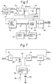
- Fig 6 represents the signals at various points in the transmitter and receiver of Figs 4 and 5.
- waveform J indicates the status of the probe contacts 11 (after the debounce provided by the status logic circuit 13).
- Waveform K shows the phase modulated 1kHz signal (before the filter 30 of Fig 1).
- At L there is indicated the short delay between the transition of the probe contacts as shown in J, and the phase inversion in the waveform K. It is this delay which is encoded in the shift register 64 of the transmitter.
- Waveform M represents the serially coded data burst on the line 70, which commences with a start bit 92, followed by an eight bit serial data word, a parity bit and a stop bit, generated in the shift register 64 with the aid of the parity generator 72.
- waveform N of Fig 6 shows the received 1kHz phase modulated signal, which is the same as waveform K in the transmitter.
- Waveform P shows clock pulses at 1kHz derived from the counter 76 and line Q shows the sampled values which are shifted into the shift register 80 as a result.
- line R there is a representation of the delay value which is latched into the counter 86 in the receiver, which corresponds to the transmitter delay value shown in line L.
- Fig 7 shows an improvement to the decoder circuitry in the receiver of Fig 5. It shows in more detail the phase locked loop around the oscillator 74 of the receiver. It would be normal for such a phase locked loop to include a low pass filter 100 between the output of the phase comparator 78 and the input of the voltage control oscillator 74, connected as shown by a dotted line 102 in Fig 7. This filter controls the time constant of the phase locked loop, stabilising the loop by removing small changes in the output of the phase comparator caused by minor variations in the phase error.
- the normal connection 102 is replaced by a sample and hold circuit 104.
- the sample and hold circuit 104 feeds the output of the filter 100 straight through to the input of the voltage controlled oscillator 74, so that the phase locked loop works in the normal way.
- the phase errors introduced by the amplifiers and filters can be tolerated in this condition.
- the sample and hold circuit 104 is integrating the output of the filter 100, and causing an average value for the oscillator input to be stored on a capacitor 106, with a long time constant compared to the filter 100.
- control logic 84 (Fig 5) detects the beginning of a data burst, it provides an input to the sample and hold circuit 104 on a line 108. This causes the sample and hold circuit to cease feeding through the output of the filter 100, and instead to sample the integrated average value held on the capacitor 106. This stable value is held constant throughout the data burst and throughout the decoding sequence. Thus, during the decoding the frequency of the oscillator is held very stable, removing phase errors caused in the amplifiers and filters, and giving a high repeatability.
- the relatively low time constant of the filter 100 continues to govern the phase locked loop, so that the loop can react to any changes in frequency and so that there is no risk of the phase locked loop ceasing to track the frequency of the oscillator in the transmitter.
Abstract
Description
- This invention relates to probes for use on machines which determine a position of a workpiece, such as coordinate measuring machines and machine tools. More particularly, it relates to signal transmission systems for such probes.
- A trigger probe for such purposes is described in US patent 4,153,998 (McMurtry). In use, the probe is moved by the machine relative to a workpiece. The probe has a deflectable stylus, and delivers a trigger signal when the stylus contacts the workpiece. The trigger signal is indicated by the probe switching from one state to another. The trigger signal is used by the control of the machine to freeze the outputs of scales or other measuring means which indicate the position of the probe. The position of the point of contact on the workpiece surface can thus be determined.
- Especially on machine tools, it can be difficult to wire the probe directly to the machine control, and so various wireless signal transmission systems have been developed in the prior art. These include inductive systems (where the signal is transmitted by electro-magnetic induction between two coils); optical systems (where an optical emitter such an infra-red diode is provided on the probe and produces an optical signal which is received by an appropriate receiver); and radio systems (having a radio transmitter in the probe and a radio receiver fixed at a convenient location on the machine). An example of an optical system is shown in European Patent Application EP 337,671 (Renishaw). An example of a radio system is shown in US Patent 4,118,871 (Kearney & Trecker).
- An important requirement of such probes is repeatability, i.e. that the same result should be achieved every time a given measurement is repeated. The mechanical position of the stylus in the probes described in US patent 4,153,998 is extremely repeatable in space, and the instant of production of the trigger signal always has a definite, repeatable relationship with the instant of contact between the stylus and the workpiece. This means that accurate results can be obtained from the probe by a simple calibration procedure.
- However, the accuracy would be destroyed if the signal transmission system were not repeatable, that is, if there were an unknown, variable delay in the signal transmission. If this occurs, then the probe will travel an unknown, variable distance after the instant of generation of the trigger signal before the machine control is able to freeze the outputs of the measuring means. There is then an error between the position of contact and the position indicated by the frozen outputs, and this error is an unknown, variable quantity which cannot be removed by calibration. Thus, in order to maintain the overall accuracy of the probe system, there is the problem of ensuring that any transmission delays introduced by the signal transmission system are repeatable, i.e. the same delay should be introduced every time the probe is triggered. The probe calibration procedure mentioned above will then also remove this repeatable delay caused by the transmission system.
- In the case of radio transmission systems, a further problem is that the bandwidth of the signal must be kept to a minimum, so as to comply with official regulations and reduce the likelihood of causing interference. Unfortunately, the requirement for a small bandwidth can conflict with the requirement for repeatable signal transmission, because to transmit a fast signal at a desired instant of time requires a relatively high bandwidth.
- One commercially available radio probe transmission system, for example, used a frequency shift keying method. Modulated onto the radio frequency carrier is one of two possible audio signals, having two different frequencies representing the two possible states of the probe. The trigger signal is indicated by a change of the audio signal from one frequency to the other when the probe changes state. However, the receiver of this system has difficulty in detecting the trigger signal in a repeatable manner, since the minimum time required to recognise the change from one audio frequency to the other is one cycle of the audio frequency, and probably two cycles. It is impossible for the receiver to know at what time during the previous cycle the change of state in the probe occurred. The uncertainty in the detection of the trigger signal, therefore, is at least one quarter of a cycle of the audio signal, giving rise to a corresponding degree of non-repeatability. If the audio frequency is increased to reduce this problem, the bandwidth would also be increased.
- One aspect of the present invention provides a signal transmission system for a probe for a position determination machine, comprising a transmitter for mounting with the probe, and a receiver for mounting on the machine for receiving the signal transmitted by the transmitter, and including:
master reference means in the transmitter for producing a master reference signal having a reference frequency;
slave reference means in the receiver for producing a slave reference signal which is synchronised with respect to said reference frequency;
carrier signal generating means in the transmitter for producing a carrier signal which is synchronised with respect to said reference frequency;
means in the transmitter for modulating a probe signal onto said carrier signal;
means in the receiver for receiving said modulated carrier signal; and
means in the receiver for demodulating said probe signal from said modulated carrier signal, synchronously with the slave reference signal. - Preferably the modulating means is a phase modulating means for modulating the probe signal onto the carrier signal.
- In preferred embodiments of this aspect of the invention, because the signal transmission system has a separate reference signal for keeping synchronism between the transmitter and the receiver, it is possible to detect the switching between one state of the probe output and the other state thereof more quickly and reliably than in the above mentioned commercially available radio transmission system. Moreover, compared with the system of EP 337,671, it is possible to ensure that synchronism is not lost even if there should be external interference at the time of a switching event, and the receiver can thus determine the current state of the probe output even after such interference. Furthermore, such a system can be realised with a relatively low bandwidth, if desired for a radio transmission system.
- A second aspect of the present invention provides a signal transmission system for a probe for a position determination machine, comprising a transmitter for mounting with the probe, and a receiver for mounting on the machine for receiving the signal transmitted by the transmitter, and including:
carrier signal generating means in the transmitter for producing a carrier signal for transmission to the receiver;
means in the transmitter for modulating a probe signal onto the carrier signal;
timer means in the transmitter for determining the time of occurrence of a probe signal;
means for transmitting data representing the time determined by the timer means; and
means in the receiver for receiving said data representing the time and producing a probing output signal derived therefrom. - At least in one preferred embodiment of the invention, this enables the modulation of the carrier to change state at a defined transition point in the carrier cycle, while still passing time information as to whereabouts within the carrier cycle the probing signal occurred. It is possible to transmit the time information without greatly increasing the bandwidth of the signal.
- Preferred embodiments of the present invention will now be described by way of example, with reference to the accompanying drawings, wherein:
- Fig 1 is a block circuit diagram of a transmitter in a first signal transmission system according to the invention,
- Fig 2 is a block circuit diagram of a receiver for the first signal transmission system,
- Fig 3 is a timing diagram showing the signals at various points in the circuits of Figs 1 and 2,
- Fig 4 is a block circuit diagram of a transmitter for a second signal transmission system according to the invention,
- Fig 5 is a block circuit diagram of a receiver for the second signal transmission system,
- Fig 6 is a timing diagram showing the signals at various points in the circuits of Figs 4 and 5, and
- Fig 7 is a circuit diagram of a modification of the receiver of Fig 5.
- Referring to Fig 1, a
touch trigger probe 10 constructed in accordance with US patent 4,153,998 includes kinematically arranged seating elements formingelectrical contacts 11. Although only one set ofelectrical contacts 11 is shown, it will be appreciated that there are three such sets, connected in series in a normally closed circuit, which is opened when adeflectable stylus 12 of theprobe 10 contacts a workpiece. The opening and closing of these contacts is detected by astatus logic circuit 13, which provides debouncing and controls anelectronic switch 14. - A voltage controlled
oscillator 16 produces a square wave output which is nominally 1 kHz. This is shown as waveform A in Fig 3, and is used as a carrier signal. The precise frequency of theoscillator 16 depends upon the battery voltage VB of theprobe 10, enabling information to be transmitted to the receiver of the signal transmission system about the condition of the battery. The frequency shift in theoscillator 16 may be, for example, 100 Hz for the full range of possible battery voltage which is to be monitored, e.g. 2 volts. - The output of the
oscillator 16 is fed to adivider 18, which divides it by 2, giving a 500 Hz output which has a definite phase relationship to the 1 kHz signal, shown as waveform B in Fig 3. The 1 kHz carrier signal from theoscillator 16 and the 500 Hz signal from thedivider 18 are each filtered by respective band pass filters 20,22, giving sinusoidal outputs which are mixed together in amixer 24. The resulting signal is fed to a conventionalFM transmitter circuit 26, where it is modulated onto a radio frequency carrier wave and transmitted as a radio signal from an aerial 32 in theprobe 10. The narrow filters 20,22 limit the bandwidth of the radio signal, to comply with official regulations and to prevent the transmitter from interfering with other nearby equipment. - The
filters oscillator 16 due to battery voltage change. - In order to encode the signal from the
contacts 11 onto the signals described, the output of the 1kHz filter 20 is fed to themixer 24 either directly, or via aninverter 28, under the control of theelectronic switch 14. Thus, when theprobe contacts 11 are opened as a result of deflection of thestylus 12, the 1 kHz frequency is phase-shifted by 180°. Alow pass filter 30 is provided at the output of theelectronic switch 14, in order to limit the rise time of the data signal which results when theprobe contacts 11 change state. Again, this is to limit the bandwidth of the transmitted signal. - Waveform C in Fig 3 represents the resulting signal at the output of the
electronic switch 14, assuming that the signal D is produced from thecontacts 11. (Waveform C is shown in an idealised form, taking no account of thefilters 20,30). It will be seen that there is a 180° change of phase at points P and R, corresponding to the instants at which theprobe contacts 11 open and close respectively, when a workpiece is probed by thestylus 12 and when thestylus 12 subsequently reseats as it is moved out of contact with the workpiece. - If desired, the
filters filter 30. Such a filter would have a pass band determined by the necessary bandwidth for the data signal from thecontacts 11. In practice, the signal from thecontact 11 will be relatively fast. The use of aseparate filter 20 for the 1 kHz signal, rather than such a combined filter, makes it easier to limit the spectrum of the transmitter. - The signal transmitted from the aerial 32 in the transmitter is received by an aerial 34 of a receiver circuit shown in Fig 2, which is mounted at a convenient fixed location on the machine to which the
probe 10 is fitted. The radio signal is demodulated by anFM detector 36, which suitably may use the signal strength of the radio carrier frequency received to tune accurately the local oscillator within theFM detector 36 for best reception. Thedetector 36 thus delivers an audio signal containing the code shown in waveform C of Fig 3. - At the output of the
detector 36, alow pass filter 38 separates out the 500Hz signal and sends it to a batteryvoltage monitor circuit 40. This circuit provides an output signal when the battery voltage is getting low, to warn the operator of the machine that the probe battery should be changed. - A
high pass filter 42 separates out the 1 kHz signal from the audio output of thedetector 36. The outputs of the twofilters decoder 44. - The
decoder 44 includes a 1 kHz voltage controlledoscillator 46, the output of which is divided by 2 in adivider 48 and then compared with the 500Hz signal from thefilter 38 in aphase comparator 50. The result is fed back to the control input of theoscillator 46 thus forming a phase locked loop. Theoscillator 46 thus recreates the original 1kHz signal produced by theoscillator 16 in the transmitter, shown as waveform A in Fig 3. This is compared with the output of thehigh pass filter 42 in aphase comparator 52. The resulting phase comparison signal contains the information from theprobe contacts 11. - The output from the
phase comparator 52 is shown as waveform E in Fig 3. It can be seen that the base line of this signal is zero when the probe contacts are closed, and 1 when the probe contacts are open. There is a difficulty, however, in that there are small transitions or spikes 56 in the signal due to phase error and to phase detector error. To overcome this problem, the signal is analysed digitally in asoftware filter 54. At each of thespikes 56, a software timer is activated which has a fixed period slightly longer than the duration of the spike. At the end of the fixed period, the signal is analysed by the software to see if a change of state has occurred, corresponding to a change in the state of theprobe contacts 11. If such a change of state has indeed occurred, the output signal of the software filter is activated, a fixed delay after the corresponding transition in the input to the filter. It will be appreciated that the delay thus introduced does not cause a problem, as long as it is repeatable, since it is calibrated out by the usual calibration procedure when theprobe 10 is used. - In place of the
software filter 54, equivalent digital hardware could be used, e.g. using a monostable instead of a software timer. Alternatively, instead of analysing digital signals it is possible to analyse sinusoidal signals at the outputs of thefilters contacts 11 occurs can be deduced by comparing the relative amplitudes of the sinusoidal signals. - An important advantage of the transmitter and receiver systems described above is that the resulting output of the receiver indicates at all times the status of the contacts 11 (open or closed). This is possible because the 500Hz signal provides a phase reference against which the relative phase of the 1kHz signal can be judged. This means that information as to the current status of the probe contacts is always available, so that the machine control to which the receiver is connected is provided with reliable information as to whether the probe is ready for probing a workpiece, or is already in contact with the workpiece. Without such a phase reference, it would only be possible to detect changes in phase in the 1kHz signal, which would be unreliable if interference occurred at the time of a change of state of the
contacts 11. - The second embodiment will now be described, with reference to Figs 4 to 6.
- Fig 4 shows transmitter circuits which are additional to those of Fig 1. It also shows the
probe 10 havingcontacts 11 and astatus logic circuit 13 as before. Aclock circuit 60 produces clock pulses at 256kHz. This drives a divide-by-256counter 62, giving a 1kHz output 67 and a parallel binary counter output on adata bus 66. When thestatus logic 13 indicates that theprobe contacts 11 have changed state, it provides a latch input to ashift register 64. The current value held in thecounter 62 is then loaded into theshift register 64 from thedata bus 66. - The
1kHz output 67 of thecounter 62 is taken to alogic circuit 68, which controls theshift register 64 such that when a value has been loaded into the shift register from thecounter 62, it is then transmitted serially on anoutput line 70, as a burst of serially coded binary data. At the same time as the loading of the data value into theshift register 64, the same value is loaded into aparity generator circuit 72, which provides a parity bit which is added to the end of the data burst. Start and stop bits are also added to the data burst. - The data signal on the
line 70 is used to control theelectronic switch 14 of Fig 1, in place of the direct connection shown in Fig 1 between thestatus logic circuit 13 and theelectronic switch 14. Thus, the serial data signal produces a phase modulation of the 1kHz sine wave, which is combined with the 500Hz reference signal and modulated onto the radio output signal. - The
1kHz output 67 of thecounter 62 is used in place of the1kHz oscillator 16 in Fig 1. Thus, theclock 60 provides the time standard for the entire system, and the counter output on thedata bus 66 at any given time is a count of the elapsed time since the beginning of the 1kHz cycle. In particular, the value latched into theshift register 64 indicates the time elapsed between the start of the 1 kHz cycle and the change of state of theprobe contacts 11. - Fig 5 shows a receiver circuit for use in decoding the signals produced by the transmitter of Fig 4. As in Fig 2, the receiver comprises an FM detector (not shown in Fig 5) which demodulates the radio frequency signals received, and filters 38,42 which separate out the 500Hz and 1kHz signals respectively. A local voltage controlled
oscillator 74 produces a 256kHz output, which is divided by 512 in adivider 76 to give a 500Hz output. Theoscillator 74 has aphase comparator 78 at its input, which compares the 500Hz output of thedivider 76 with the 500Hz reference signal from thefilter 38, thus ensuring that theoscillator 74 is permanently synchronised with theclock 60 in the transmitter. The circuit is a phase locked loop, as previously. - The
divider 76 also provides a 1kHz output, which drives the clock input of ashift register 80. Theshift register 80 receives the 1kHz signal from thefilter 42, onto which the serial data is phase modulated. As theshift register 80 is clocked at 1kHz by thedivider 76, this causes the serial data to be sampled. Corresponding data bits are shifted into the shift register and stored, depending on the phase of the 1kHz output from thefilter 42 at the instant of each 1kHz clock input pulse. - The
shift register 80 produces a parallel output on adata bus 82. During steady state operation, all the lines in this bus will be at logic level zero, indicating that theprobe contacts 11 have been closed for a period of time; or they will all be atlogic level 1, indicating that the probe contacts have been open for a period of time. Acontrol logic circuit 84 monitors thedata bus 82, and is activated by the entry into theshift register 80 of the start of a binary burst of data which occurs when theprobe contacts 11 change state. When thecontrol logic 84 detects the end of the data burst, acircuit 85 checks the parity bit of the data, and the current contents of theshift register 80 are then loaded into acounter 86. Thus, the value now present in thecounter 86 is equal to the time value coded in the transmitter. Thecounter 86 receives clock pulses at 256kHz from theoscillator 74, in phase with the clock pulses in the transmitter, and now counts downwards at this rate until the value held in the counter reaches zero. When this happens, alatch 88 changes state, and this latch controls asolid state relay 90 which generates the output signal to the machine control which indicates that theprobe contacts 11 have changed state. - It will be appreciated that the length of time taken for the
counter 86 to count down to zero is equal to the length of time latched into theshift register 64 in the transmitter, which indicates the time period between the start of a 1kHz cycle of the system and the change of state of theprobe contacts 11. We have found that despite the low bandwidth of the system, nevertheless the circuits described above make it possible for the256kHz oscillator 74 to be very precisely synchronised with the256kHz clock 60 in the transmitter, and for the 1kHz output of thedivider 76 in the receiver to be in a very precise phase relationship with the1kHz signal 67. As a result, although the delay between the probe contact status change and the corresponding output signal from therelay 90 is relatively long, about 11 milliseconds, nevertheless the delay involved is very precisely repeatable (i.e. it is precisely the same every time theprobe contacts 11 change state), to within a few microseconds. Thus, a high degree of repeatability of the signal is achieved despite the low bandwidth. - Fig 6 represents the signals at various points in the transmitter and receiver of Figs 4 and 5. In this Figure, waveform J indicates the status of the probe contacts 11 (after the debounce provided by the status logic circuit 13). Waveform K shows the phase modulated 1kHz signal (before the
filter 30 of Fig 1). At L, there is indicated the short delay between the transition of the probe contacts as shown in J, and the phase inversion in the waveform K. It is this delay which is encoded in theshift register 64 of the transmitter. - Waveform M represents the serially coded data burst on the
line 70, which commences with astart bit 92, followed by an eight bit serial data word, a parity bit and a stop bit, generated in theshift register 64 with the aid of theparity generator 72. - In the receiver, waveform N of Fig 6 shows the received 1kHz phase modulated signal, which is the same as waveform K in the transmitter. Waveform P shows clock pulses at 1kHz derived from the
counter 76 and line Q shows the sampled values which are shifted into theshift register 80 as a result. In line R, there is a representation of the delay value which is latched into thecounter 86 in the receiver, which corresponds to the transmitter delay value shown in line L. When thecounter 86 produces an output at the end of this delay, therelay 90 produces an output signal shown as waveform S. - Fig 7 shows an improvement to the decoder circuitry in the receiver of Fig 5. It shows in more detail the phase locked loop around the
oscillator 74 of the receiver. It would be normal for such a phase locked loop to include alow pass filter 100 between the output of thephase comparator 78 and the input of thevoltage control oscillator 74, connected as shown by a dottedline 102 in Fig 7. This filter controls the time constant of the phase locked loop, stabilising the loop by removing small changes in the output of the phase comparator caused by minor variations in the phase error. - Necessarily there are a number of amplifiers and filters in the FM radio transmission and receiving circuits, and also the
filters filter 100. Unfortunately, to do so would increase the instability of the phase locked loop decreasing its ability to track variations in the transmitter clock. A simple increase in the time constant is therefore not practicable. - In the present modification, therefore, the
normal connection 102 is replaced by a sample and holdcircuit 104. In the normal operation of the circuit, when there is no change in status of theprobe contacts 11, the sample and holdcircuit 104 feeds the output of thefilter 100 straight through to the input of the voltage controlledoscillator 74, so that the phase locked loop works in the normal way. The phase errors introduced by the amplifiers and filters can be tolerated in this condition. Nevertheless, throughout this condition, the sample and holdcircuit 104 is integrating the output of thefilter 100, and causing an average value for the oscillator input to be stored on acapacitor 106, with a long time constant compared to thefilter 100. When the control logic 84 (Fig 5) detects the beginning of a data burst, it provides an input to the sample and holdcircuit 104 on aline 108. This causes the sample and hold circuit to cease feeding through the output of thefilter 100, and instead to sample the integrated average value held on thecapacitor 106. This stable value is held constant throughout the data burst and throughout the decoding sequence. Thus, during the decoding the frequency of the oscillator is held very stable, removing phase errors caused in the amplifiers and filters, and giving a high repeatability. Nevertheless, as soon as the decoding sequence has finished, the relatively low time constant of thefilter 100 continues to govern the phase locked loop, so that the loop can react to any changes in frequency and so that there is no risk of the phase locked loop ceasing to track the frequency of the oscillator in the transmitter.
Claims (4)
- A signal transmission system for a probe (10) for a position determination machine, comprising a transmitter for mounting with the probe, and a receiver for mounting on the machine for receiving the signal transmitted by the transmitter, and including:
carrier signal generating means (60,62) in the transmitter for producing a carrier signal for transmission to the receiver;
means (14) in the transmitter for modulating a probe signal onto the carrier signal;
timer means (62,64,68) in the transmitter for determining the time of occurrence of a probe signal;
means (64,68,72) for transmitting data representing the time determined by the timer means; and
means (80,84,86) in the receiver for receiving said data representing the time and producing a probing output signal derived therefrom. - A signal transmission system according to claim 1, including:
carrier receiving means (38,42,74,76,78) in the receiver, for receiving the transmitted carrier signal in a synchronised relationship therewith, such that a point in the cycle of the carrier signal in the receiver corresponds to a point in the cycle of the carrier signal in the transmitter;
wherein said timer means comprises means (62,64,68) for measuring the time delay between the instant of a probe signal and the instant of said point in the carrier cycle in the transmitter;
and wherein said means (80,84,86) in the receiver for receiving said data representing the time derives said probing output signal from the measured time delay and said point in the receiver carrier cycle. - A signal transmission system according to claim 1 or claim 2, wherein the means (64,68,72) for transmitting the data representing the time encodes said time as serial data.
- A signal transmission system according to any one of the preceding claims, wherein said transmitter is a radio transmitter and said receiver is a radio receiver.
Applications Claiming Priority (3)
| Application Number | Priority Date | Filing Date | Title |
|---|---|---|---|
| FR9104141A FR2674659A1 (en) | 1991-03-29 | 1991-03-29 | SIGNAL TRANSMISSION DEVICE FOR TRIGGERED PROBE. |
| FR9104141 | 1991-03-29 | ||
| EP92302471A EP0506318B1 (en) | 1991-03-29 | 1992-03-23 | Signal transmission system for trigger probe |
Related Parent Applications (2)
| Application Number | Title | Priority Date | Filing Date |
|---|---|---|---|
| EP92302471.5 Division | 1992-03-23 | ||
| EP92302471A Division EP0506318B1 (en) | 1991-03-29 | 1992-03-23 | Signal transmission system for trigger probe |
Publications (3)
| Publication Number | Publication Date |
|---|---|
| EP0652413A2 true EP0652413A2 (en) | 1995-05-10 |
| EP0652413A3 EP0652413A3 (en) | 1996-06-12 |
| EP0652413B1 EP0652413B1 (en) | 1998-07-29 |
Family
ID=9411501
Family Applications (2)
| Application Number | Title | Priority Date | Filing Date |
|---|---|---|---|
| EP92302471A Expired - Lifetime EP0506318B1 (en) | 1991-03-29 | 1992-03-23 | Signal transmission system for trigger probe |
| EP95200123A Expired - Lifetime EP0652413B1 (en) | 1991-03-29 | 1992-03-23 | Signal transmission system for trigger probe |
Family Applications Before (1)
| Application Number | Title | Priority Date | Filing Date |
|---|---|---|---|
| EP92302471A Expired - Lifetime EP0506318B1 (en) | 1991-03-29 | 1992-03-23 | Signal transmission system for trigger probe |
Country Status (5)
| Country | Link |
|---|---|
| US (1) | US5279042A (en) |
| EP (2) | EP0506318B1 (en) |
| JP (1) | JP3126797B2 (en) |
| DE (2) | DE69203770T2 (en) |
| FR (1) | FR2674659A1 (en) |
Cited By (1)
| Publication number | Priority date | Publication date | Assignee | Title |
|---|---|---|---|---|
| EP2533022A1 (en) * | 2011-06-10 | 2012-12-12 | Hexagon Technology Center GmbH | Extremely precise synchronised measuring value recording |
Families Citing this family (16)
| Publication number | Priority date | Publication date | Assignee | Title |
|---|---|---|---|---|
| GB9305687D0 (en) * | 1993-03-19 | 1993-05-05 | Renishaw Metrology Ltd | A signal processing for trigger probe |
| US5517190A (en) * | 1994-02-03 | 1996-05-14 | Gunn; Colin N. | Physical measurement from changes in reactance |
| ITBO940167A1 (en) * | 1994-04-19 | 1995-10-19 | Marposs Spa | SYSTEM FOR DETECTION OF LINEAR DIMENSIONS AND METHOD FOR VERIFYING THE RELATIVE OPERATION |
| GB9415338D0 (en) * | 1994-07-29 | 1994-09-21 | Renishaw Plc | Trigger probe circuit |
| IT1279590B1 (en) * | 1995-05-11 | 1997-12-16 | Marposs Spa | SYSTEM AND METHOD OF TRANSMISSION OF SIGNALS VIA ETHER BETWEEN A CONTROL HEAD AND A REMOTE RECEIVER |
| US5777562A (en) * | 1996-08-19 | 1998-07-07 | Hoffman; David J. | Centering device and method for centering |
| TW376598B (en) * | 1997-02-05 | 1999-12-11 | Em Microelectronic Marin Sa | Base station for a contactless interrogation system comprising a phase locked and voltage controlled oscillator |
| GB9802767D0 (en) * | 1998-02-11 | 1998-04-08 | Renishaw Plc | Signal transmission circuit for probe |
| JP2000052196A (en) * | 1998-08-08 | 2000-02-22 | Nt Engineering Kk | Work machine and communication method thereof |
| DE10132554B4 (en) | 2001-07-04 | 2011-07-07 | Dr. Johannes Heidenhain GmbH, 83301 | Method for operating a touch probe and probe system for carrying out the method |
| GB0229763D0 (en) * | 2002-12-23 | 2003-01-29 | Renishaw Plc | Signal transmission system for a trigger probe |
| US8849221B2 (en) * | 2012-11-16 | 2014-09-30 | Mstar Semiconductor, Inc. | Direct conversion transmitter and communication system utilizing the same |
| US10215547B2 (en) | 2016-06-24 | 2019-02-26 | Mitutoyo Corporation | Method for operating a coordinate measuring machine |
| US9970744B2 (en) | 2016-06-24 | 2018-05-15 | Mitutoyo Corporation | Method for operating a coordinate measuring machine |
| JP6800368B1 (en) * | 2020-07-07 | 2020-12-16 | Dmg森精機株式会社 | Machine tools, machine tool control methods, and machine tool control programs |
| CN112757631B (en) * | 2020-12-21 | 2022-11-11 | 深圳市创想三维科技股份有限公司 | Automatic leveling device of 3D printer and 3D printer |
Citations (6)
| Publication number | Priority date | Publication date | Assignee | Title |
|---|---|---|---|---|
| GB2025073A (en) * | 1978-07-07 | 1980-01-16 | Rolls Royce | Apparatus for Monitoring the State of an Electrical Circuit |
| EP0029499A1 (en) * | 1979-11-24 | 1981-06-03 | Ernst Leitz Wetzlar Gmbh | Data logger for test specimens |
| GB2141365A (en) * | 1983-06-14 | 1984-12-19 | Gte Valeron Corp | Method and apparatus for performing workpiece inspection with a probe |
| WO1989005435A1 (en) * | 1987-12-05 | 1989-06-15 | Renishaw Plc | Position sensing probe |
| EP0337671A2 (en) * | 1988-04-12 | 1989-10-18 | Renishaw plc | Signal transmission system for machine tools, inspection machines, and the like |
| EP0268689B1 (en) * | 1986-06-05 | 1993-03-24 | FUKUHISA, Norio | Position detector with radio transmitter and receiver |
Family Cites Families (9)
| Publication number | Priority date | Publication date | Assignee | Title |
|---|---|---|---|---|
| US4153998A (en) * | 1972-09-21 | 1979-05-15 | Rolls-Royce (1971) Limited | Probes |
| GB1487207A (en) * | 1974-09-09 | 1977-09-28 | Pye Ltd | Paging receivers |
| US4130941A (en) * | 1975-03-20 | 1978-12-26 | Rolls-Royce Limited | Displacement gauge |
| US4145816A (en) * | 1977-11-21 | 1979-03-27 | Kearney & Trecker Corporation | Spindle probe with orbital transformer |
| US4118871A (en) * | 1978-06-13 | 1978-10-10 | Kearney & Trecker Corporation | Binary inspection probe for numerically controlled machine tools |
| JPS5561163A (en) * | 1978-10-31 | 1980-05-08 | Nec Corp | Demodulation circuit for synchronous data transmission signal |
| US5065035A (en) * | 1981-04-30 | 1991-11-12 | Gte Valenite Corporation | Optical data system having flash/receiver head for energizing/receiving information from a battery operated transmitter |
| US4658509A (en) * | 1985-09-12 | 1987-04-21 | Gte Valeron Corporation | Probe having low battery detection/transmission feature |
| GB2202715B (en) * | 1987-03-24 | 1991-03-20 | Dr Frank Robert Connor | Minimum relative shift keying |
-
1991
- 1991-03-29 FR FR9104141A patent/FR2674659A1/en active Pending
-
1992
- 1992-03-23 DE DE69203770T patent/DE69203770T2/en not_active Expired - Fee Related
- 1992-03-23 DE DE69226451T patent/DE69226451T2/en not_active Expired - Lifetime
- 1992-03-23 EP EP92302471A patent/EP0506318B1/en not_active Expired - Lifetime
- 1992-03-23 EP EP95200123A patent/EP0652413B1/en not_active Expired - Lifetime
- 1992-03-25 US US07/857,279 patent/US5279042A/en not_active Expired - Lifetime
- 1992-03-30 JP JP04074746A patent/JP3126797B2/en not_active Expired - Fee Related
Patent Citations (6)
| Publication number | Priority date | Publication date | Assignee | Title |
|---|---|---|---|---|
| GB2025073A (en) * | 1978-07-07 | 1980-01-16 | Rolls Royce | Apparatus for Monitoring the State of an Electrical Circuit |
| EP0029499A1 (en) * | 1979-11-24 | 1981-06-03 | Ernst Leitz Wetzlar Gmbh | Data logger for test specimens |
| GB2141365A (en) * | 1983-06-14 | 1984-12-19 | Gte Valeron Corp | Method and apparatus for performing workpiece inspection with a probe |
| EP0268689B1 (en) * | 1986-06-05 | 1993-03-24 | FUKUHISA, Norio | Position detector with radio transmitter and receiver |
| WO1989005435A1 (en) * | 1987-12-05 | 1989-06-15 | Renishaw Plc | Position sensing probe |
| EP0337671A2 (en) * | 1988-04-12 | 1989-10-18 | Renishaw plc | Signal transmission system for machine tools, inspection machines, and the like |
Cited By (6)
| Publication number | Priority date | Publication date | Assignee | Title |
|---|---|---|---|---|
| EP2533022A1 (en) * | 2011-06-10 | 2012-12-12 | Hexagon Technology Center GmbH | Extremely precise synchronised measuring value recording |
| WO2012168294A3 (en) * | 2011-06-10 | 2013-05-30 | Hexagon Technology Center Gmbh | High precision synchronized measured value acquisition |
| CN103608647A (en) * | 2011-06-10 | 2014-02-26 | 赫克斯冈技术中心 | High precision synchronized measured value acquisition |
| US9077513B2 (en) | 2011-06-10 | 2015-07-07 | Hexagon Technology Center Gmbh | High precision synchronized measured value acquisition |
| KR101606043B1 (en) | 2011-06-10 | 2016-03-24 | 헥사곤 테크놀로지 센터 게엠베하 | High precision synchronized measured value acquisition |
| CN103608647B (en) * | 2011-06-10 | 2016-06-01 | 赫克斯冈技术中心 | The measured value of high-precise synchronization obtains |
Also Published As
| Publication number | Publication date |
|---|---|
| JPH0589397A (en) | 1993-04-09 |
| EP0506318A1 (en) | 1992-09-30 |
| EP0652413A3 (en) | 1996-06-12 |
| US5279042A (en) | 1994-01-18 |
| DE69226451T2 (en) | 1998-12-10 |
| DE69203770T2 (en) | 1995-12-07 |
| JP3126797B2 (en) | 2001-01-22 |
| DE69226451D1 (en) | 1998-09-03 |
| DE69203770D1 (en) | 1995-09-07 |
| EP0652413B1 (en) | 1998-07-29 |
| EP0506318B1 (en) | 1995-08-02 |
| FR2674659A1 (en) | 1992-10-02 |
Similar Documents
| Publication | Publication Date | Title |
|---|---|---|
| EP0506318B1 (en) | Signal transmission system for trigger probe | |
| US4052722A (en) | Traffic radar and apparatus therefor | |
| CA1240770A (en) | Radar warning receiver | |
| US4178549A (en) | Recognition of a received signal as being from a particular transmitter | |
| US9077513B2 (en) | High precision synchronized measured value acquisition | |
| US4313183A (en) | Acoustic distance measuring method and apparatus | |
| JP3696886B2 (en) | A system for measuring jitter in non-binary digital signals. | |
| US4704574A (en) | Phase difference measurement apparatus and method | |
| US4631543A (en) | Method and apparatus for reducing the effects of impulse noise in Loran-C receivers | |
| JP3647464B2 (en) | Apparatus and method for wireless transmission of signals between a measuring head and a remote receiver | |
| EP0297719A2 (en) | Device for synchronizing the output pulses of a circuit with an input clock | |
| US4100531A (en) | Bit error rate measurement above and below bit rate tracking threshold | |
| US7379395B2 (en) | Precise time measurement apparatus and method | |
| US5144312A (en) | Locating system | |
| US3298024A (en) | Method and device for distance measuring with the aid of electric waves | |
| US9823646B2 (en) | Device and method for generating a trigger signal in a position-measuring device and corresponding position-measuring device | |
| US4722004A (en) | Video signal discriminating apparatus | |
| US4801896A (en) | Circuit providing improved lock-in for a phase-locked loop | |
| US3934254A (en) | Reliable cycle selection in LORAN-C system | |
| JP2001517301A (en) | Simulator for testing anti-collision radar systems | |
| EP0546723A1 (en) | Radio frequency receiver | |
| US6292524B1 (en) | Counting apparatus and rotation stopped detection apparatus which uses a counting apparatus | |
| EA006324B1 (en) | Method for determining and/or monitoring the distance from an object and device therefor | |
| JPS62251683A (en) | Positioning device by transponder | |
| US3631487A (en) | Complementary search system for d.m.e. |
Legal Events
| Date | Code | Title | Description |
|---|---|---|---|
| PUAI | Public reference made under article 153(3) epc to a published international application that has entered the european phase |
Free format text: ORIGINAL CODE: 0009012 |
|
| 17P | Request for examination filed |
Effective date: 19950119 |
|
| AC | Divisional application: reference to earlier application |
Ref document number: 506318 Country of ref document: EP |
|
| AK | Designated contracting states |
Kind code of ref document: A2 Designated state(s): CH DE FR GB IT LI |
|
| PUAL | Search report despatched |
Free format text: ORIGINAL CODE: 0009013 |
|
| AK | Designated contracting states |
Kind code of ref document: A3 Designated state(s): CH DE FR GB IT LI |
|
| 17Q | First examination report despatched |
Effective date: 19970110 |
|
| GRAG | Despatch of communication of intention to grant |
Free format text: ORIGINAL CODE: EPIDOS AGRA |
|
| GRAG | Despatch of communication of intention to grant |
Free format text: ORIGINAL CODE: EPIDOS AGRA |
|
| GRAH | Despatch of communication of intention to grant a patent |
Free format text: ORIGINAL CODE: EPIDOS IGRA |
|
| GRAH | Despatch of communication of intention to grant a patent |
Free format text: ORIGINAL CODE: EPIDOS IGRA |
|
| GRAA | (expected) grant |
Free format text: ORIGINAL CODE: 0009210 |
|
| ITF | It: translation for a ep patent filed |
Owner name: BARZANO' E ZANARDO MILANO S.P.A. |
|
| AC | Divisional application: reference to earlier application |
Ref document number: 506318 Country of ref document: EP |
|
| AK | Designated contracting states |
Kind code of ref document: B1 Designated state(s): CH DE FR GB IT LI |
|
| PG25 | Lapsed in a contracting state [announced via postgrant information from national office to epo] |
Ref country code: LI Free format text: LAPSE BECAUSE OF FAILURE TO SUBMIT A TRANSLATION OF THE DESCRIPTION OR TO PAY THE FEE WITHIN THE PRESCRIBED TIME-LIMIT Effective date: 19980729 Ref country code: FR Free format text: LAPSE BECAUSE OF FAILURE TO SUBMIT A TRANSLATION OF THE DESCRIPTION OR TO PAY THE FEE WITHIN THE PRESCRIBED TIME-LIMIT Effective date: 19980729 Ref country code: CH Free format text: LAPSE BECAUSE OF FAILURE TO SUBMIT A TRANSLATION OF THE DESCRIPTION OR TO PAY THE FEE WITHIN THE PRESCRIBED TIME-LIMIT Effective date: 19980729 |
|
| REG | Reference to a national code |
Ref country code: CH Ref legal event code: EP |
|
| REF | Corresponds to: |
Ref document number: 69226451 Country of ref document: DE Date of ref document: 19980903 |
|
| EN | Fr: translation not filed | ||
| REG | Reference to a national code |
Ref country code: CH Ref legal event code: PL |
|
| PLBE | No opposition filed within time limit |
Free format text: ORIGINAL CODE: 0009261 |
|
| STAA | Information on the status of an ep patent application or granted ep patent |
Free format text: STATUS: NO OPPOSITION FILED WITHIN TIME LIMIT |
|
| 26N | No opposition filed | ||
| REG | Reference to a national code |
Ref country code: GB Ref legal event code: IF02 |
|
| PG25 | Lapsed in a contracting state [announced via postgrant information from national office to epo] |
Ref country code: IT Free format text: LAPSE BECAUSE OF NON-PAYMENT OF DUE FEES;WARNING: LAPSES OF ITALIAN PATENTS WITH EFFECTIVE DATE BEFORE 2007 MAY HAVE OCCURRED AT ANY TIME BEFORE 2007. THE CORRECT EFFECTIVE DATE MAY BE DIFFERENT FROM THE ONE RECORDED. Effective date: 20050323 |
|
| PGRI | Patent reinstated in contracting state [announced from national office to epo] |
Ref country code: IT Effective date: 20080301 |
|
| PGFP | Annual fee paid to national office [announced via postgrant information from national office to epo] |
Ref country code: GB Payment date: 20090325 Year of fee payment: 18 |
|
| GBPC | Gb: european patent ceased through non-payment of renewal fee |
Effective date: 20100323 |
|
| PG25 | Lapsed in a contracting state [announced via postgrant information from national office to epo] |
Ref country code: GB Free format text: LAPSE BECAUSE OF NON-PAYMENT OF DUE FEES Effective date: 20100323 |
|
| PGFP | Annual fee paid to national office [announced via postgrant information from national office to epo] |
Ref country code: DE Payment date: 20110325 Year of fee payment: 20 |
|
| PGFP | Annual fee paid to national office [announced via postgrant information from national office to epo] |
Ref country code: IT Payment date: 20110329 Year of fee payment: 20 |
|
| REG | Reference to a national code |
Ref country code: DE Ref legal event code: R071 Ref document number: 69226451 Country of ref document: DE |
|
| REG | Reference to a national code |
Ref country code: DE Ref legal event code: R071 Ref document number: 69226451 Country of ref document: DE |
|
| PG25 | Lapsed in a contracting state [announced via postgrant information from national office to epo] |
Ref country code: DE Free format text: LAPSE BECAUSE OF EXPIRATION OF PROTECTION Effective date: 20120324 |