EP0602422A1 - Dynamic frequency shifting with divide by one clock generators - Google Patents
Dynamic frequency shifting with divide by one clock generators Download PDFInfo
- Publication number
- EP0602422A1 EP0602422A1 EP93118893A EP93118893A EP0602422A1 EP 0602422 A1 EP0602422 A1 EP 0602422A1 EP 93118893 A EP93118893 A EP 93118893A EP 93118893 A EP93118893 A EP 93118893A EP 0602422 A1 EP0602422 A1 EP 0602422A1
- Authority
- EP
- European Patent Office
- Prior art keywords
- microprocessor
- clock signal
- external clock
- frequency
- signal
- Prior art date
- Legal status (The legal status is an assumption and is not a legal conclusion. Google has not performed a legal analysis and makes no representation as to the accuracy of the status listed.)
- Withdrawn
Links
Images

Classifications
-
- G—PHYSICS
- G06—COMPUTING; CALCULATING OR COUNTING
- G06F—ELECTRIC DIGITAL DATA PROCESSING
- G06F1/00—Details not covered by groups G06F3/00 - G06F13/00 and G06F21/00
- G06F1/04—Generating or distributing clock signals or signals derived directly therefrom
- G06F1/08—Clock generators with changeable or programmable clock frequency
-
- H—ELECTRICITY
- H04—ELECTRIC COMMUNICATION TECHNIQUE
- H04B—TRANSMISSION
- H04B2215/00—Reducing interference at the transmission system level
- H04B2215/064—Reduction of clock or synthesizer reference frequency harmonics
-
- H—ELECTRICITY
- H04—ELECTRIC COMMUNICATION TECHNIQUE
- H04B—TRANSMISSION
- H04B2215/00—Reducing interference at the transmission system level
- H04B2215/064—Reduction of clock or synthesizer reference frequency harmonics
- H04B2215/065—Reduction of clock or synthesizer reference frequency harmonics by changing the frequency of clock or reference frequency
Definitions
- the present invention relates to microprocessors having on-chip clock generators that are driven by external clock signals, and more particularly relates to such microprocessors in which the on board clock generator is a divide by one clock generator.
- Microprocessors are typically driven by quartz crystal oscillator clock signal sources that are external to the microprocessor chip itself.
- quartz crystal oscillators are very stable in frequency, which is desirable in microprocessor operation.
- the duty cycle of quartz crystal oscillators varies considerably from crystal to crystal.
- the practice that has developed in the art is to provide a quartz crystal oscillator having a frequency that is twice that needed to drive the microprocessor itself, and then provide a divide by two clock generator on the microprocessor chip itself.
- the divide by two clock generator uses only the leading edge of the quartz crystal clock signal, which is, as described above, very stable, to trigger the rising and falling transitions, thereby providing an on board clock signal that is very stable both with respect to frequency and as to duty cycle.
- a microprocessor receiving a stream of data and instructions and, in response to said instructions, operating on the data, the microprocessor including a divide by one frequency generator that receives an external clock signal and in response thereto generates an internal clock signal having the same frequency as the external clock signal but having modified characteristics, as compared to the external clock signal, and being capable of having the frequency of the external clock signal applied thereto changed without effecting the integrity of the operations of the microprocessor.
- the invention includes a non-one divider type clock generator that receives the external clock signal and in response thereto generates an internal clock signal having a fractional frequency of the external clock signal.
- An arrangement for receiving a request signal indicating a request for a change in the external clock signal frequency, and in response thereto monitoring the microprocessor to determine when a mode of operation of the microprocessor has occurred in which the processing of the data and the instruction stream can be stopped. In response to the determination that such mode has occurred, operation is switched from the divide by one clock generator to the non-one divider type generator. A ready signal is then generated indicating that the change in the external clock signal frequency can be made.
- operation is switched from the non-one divider type generator to the divide by one generator, after a period of time has occurred that is sufficient to allow the divide by one clock generator to stabilize.
- the present invention provides a dynamic frequency protocol that allows a microprocessor to contain a divide by one generator, and still have the ability to respond to a dynamic frequency shift without impacting the software stream.
- the result is that systems can still attain the power savings of frequency shifting, and still have the higher system performance of divide by one clocking as needed.
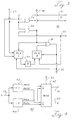
- FIG. 1 shows a microprocessor 1 according to a preferred embodiment of the present invention.
- a novel dynamic frequency shift (“DFS") subsystem 10 is shown, as well as a conventional bus state machine 50.
- Other aspects of microprocessor 1 are well known in the art. To avoid obscuring the invention, detailed description of these other aspects of microprocessor 1 will be omitted, except as necessary for an understanding of how the preferred embodiment of the DFS Subsystem 10 interfaces with and interacts with such other elements.
- DFS dynamic frequency shift
- the DFS Subsystem 10 includes three units, a DFS Interface Unit 20, a DFS Control Unit 30, and a Clock Unit 40.
- An external clock signal, CLK is received at the input 13 of the Clock Unit 40, which generates internal clock signals of two different phases which are output on lines 41 and 42.
- Clock Unit 40 includes a divide by two clock generator and a divide by one clock generator, as is discussed in detail below. It will be understood that, in general, the number of clock output signals and their relative phase are dependent upon the particular requirements of the microprocessor with which the clock unit is associated. These considerations are well known in the art and are not discussed further herein.
- the DFS Subsystem 10 receives a request that an external clock frequency shift be allowed by way of an internal request signal on line 11, DFS_REQI, and also, alternatively, by way of an external signal on line 12, DFS_ REQE, which are applied as inputs to the DFS Interface Unit 20.
- DSF_REQE is provided by the external system (not shown) in which the microprocessor operates.
- DFS_REQI is provided by an internal control register (not shown) that the system software can set.
- the DFS Subsystem 10 interfaces with the bus state machine 50 of the microprocessor 1.
- the operation of the bus state machine 50 is microprocessor dependent, and the principals that are applied thereto are well known in the art.
- the bus state machine 50 monitors internal and external requests for utilization of the microprocessor bus (not shown) and grants access depending upon whether the bus is idle.
- An external bus request signal is received on line 53
- an external bus grant signal is provided on line 54
- an internal bus request signal is received on line 55
- the internal bus grant is provided on line 56.
- a signal called BUS_IDLE which is active, i.e., 1, when the microprocessor bus is idle, is provided on line 51.
- a signal called BUS_HOLD is provided on line 31, and is activated when it is desired that the microprocessor bus, when idle, be held, that is, blocked from granting access to the bus in response to either an internal or an external bus request.
- a signal called BUS_HELD is provided on line 52.
- the signals on lines 31, 51 and 52 are utilized in conjunction with the operation of the preferred embodiment, as is discussed in detail below.
- SLOW_MODE This causes a signal called SLOW_MODE to appear on line 32, which causes a request for a switch from the divide by one clock in clock unit 40 to the divide by two clock therein.
- a DFS_RDY signal is applied to line 38 and thence to line 21.
- the external clock upon receiving the DFS_RDY signal, begins its dynamic frequency shift to a lower frequency. Since, as this is occurring, the divide by two clock is operational to provide the microprocessor internal clock signals, no disruption occurs in microprocessor operation.
- the DFS request line 11 or 12 is deactivated, i.e., goes to 0. This is communicated to the DFS control unit 30 by way of line 23. Once a sufficient period of time has passed to allow the divide by one clock in clock unit 40 to stabilize, line 32 is deactivated, causing the clock unit 40 to switch to operation using the divide by one clock generator.
- Figure 1 shows the overall interconnection of the various units of the DFS Subsystem 10
- Figure 2 which shows the internal logical structure of the DFS Interface Unit 20
- Figure 3 which shows the internal logical structure of the DFS Control Unit 30
- Figure 4 which shows the internal logical structure of the Clock Unit 40
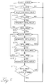
- Figure 5 which is a flow diagram showing all of the steps in the sequence of operation of the preferred embodiment in changes from fast mode to slow mode and back again to fast mode.
- Figure 6 shows the relationship between the DFS_REQ, DFS-RDY and CLK signals during a shift from a higher frequency, f1, to a lower frequency, f2.
- a request 605 is made for the BUS_HELD signal to be activated. This is accomplished by the activation of the BUS_HOLD signal line 31, as shown in Figure 3.
- AND gate 34 passes the slow mode request signal, SLOW_MODE, through OR gate 35 to signal line 32.
- the signal on line 32 is applied to the multiplexer 45 shown in Figure 4 to effect the change from the divide by one clock 43 to the divide by two clock 44.
- steps 602 and 604 show that if the DFS request signal drops out at either of those steps, the DFS shift is aborted, and the microprocessor continues in fast mode.
- steps 606 if the BUS_HELD signal is not immediately forthcoming, both BUS_IDLE and DFS_REQ must continue active, or else the shift aborts and the system remains in fast mode, as shown by the negative path from step 604.
- the subsystem is in slow mode.
- the DFS Subsystem 10 In slow mode, the DFS Subsystem 10 generates (step 608) the signal DFS-RDY which is provided on line 38 (Fig. 3) to register 24 (Fig. 2), where it is output on line 21.
- DFS_RDY Once DFS_RDY is generated, the system can change the frequency of CLK. Once this change is complete, the system remains in Slow mode until the DSF_REQ signal line 11 or 12 (Fig. 2) is deactivated 609. DFS_RDY goes to 0 at this point.
- PLA 1 then waits for the BUS_IDLE signal on line 51 (step 610) and if the DSF_REQ line remains inactive 611 a BUS_HOLD signal is generated 612.
- PLA 2 waits for the BUS_HELD signal line 52 to go inactive and waits for the clock to stabilize ( ⁇ propagation, 37) 613.
- the circuitry that permits stabilization of the clock is implemented in time delay circuit 37 in Figure 3.
- a microprocessor may be provided with a divide by one clock generator, while still having the capability of responding to a dynamic frequency shift of the external clock generator.
- Many variations and the circuitry and sequence may be made by those skilled in the art, once the principals of the invention, as expressed herein, are understood.
- the preferred embodiment set forth above operates in conjunction with a microprocessor in which the switch from SLOW_MODE to FAST_MODE and from FAST_MODE to SLOW_MODE occurs in a single cycle.
- the same signal that triggered the shift from SLOW_MODE to FAST_MODE, and vice versa was provided as the DFS_RDY signal.
- an additional gate may be required to hold off the sending of the DSF_RDY signal, pending activation of a single signal line indicating completion of the shift.
Landscapes
- Engineering & Computer Science (AREA)
- Theoretical Computer Science (AREA)
- Physics & Mathematics (AREA)
- General Engineering & Computer Science (AREA)
- General Physics & Mathematics (AREA)
- Microcomputers (AREA)
Abstract
Method and apparatus for providing a microprocessor (1) with a divide by one frequency generator (43), while permitting the external clock (CLK) driving the generator to vary in frequency without interruption of the operations of the microprocessor (1). A non-one divider type clock generator (44) is also provided on the microprocessor chip. When a change in the frequency of the external clock (CLK) is desired a request signal (11, 12) is provided to the chip. After a period of time has elapsed that permits the microprocessor (1) to achieve a "safe" mode in which processing integrity is maintained even if the clock signal (CLK) is interrupted, the non-one divider type clock generator (44) is switched into operation. The external clock (CLK) is then allowed to change frequency after which the divide by one clock generator (43) is reactivated, following a period of time sufficient to allow the divide by one clock generator (43) to stabilize.
Description
- The present invention relates to microprocessors having on-chip clock generators that are driven by external clock signals, and more particularly relates to such microprocessors in which the on board clock generator is a divide by one clock generator.
- Microprocessors are typically driven by quartz crystal oscillator clock signal sources that are external to the microprocessor chip itself. The reason for this is that quartz crystal oscillators are very stable in frequency, which is desirable in microprocessor operation. However, while very stable in frequency, it is well known that the duty cycle of quartz crystal oscillators varies considerably from crystal to crystal. As a consequence, the practice that has developed in the art is to provide a quartz crystal oscillator having a frequency that is twice that needed to drive the microprocessor itself, and then provide a divide by two clock generator on the microprocessor chip itself. The divide by two clock generator uses only the leading edge of the quartz crystal clock signal, which is, as described above, very stable, to trigger the rising and falling transitions, thereby providing an on board clock signal that is very stable both with respect to frequency and as to duty cycle.
- However, recently microprocessor technology has advanced to the point where the frequency at which microprocessors can be operated has become so great that it is impractical to utilize the traditional divide by two on board clock generator, because the external clock frequency would simply be too high to permit the provision of practical circuitry therefore. Accordingly, sophisticated divide by one clock generators, incorporating phase lock loops or delay line clock generators, have been provided. These new clock macros have the advantage of operating the internal logic at divide by one speed versus the traditional divide by two mode. However these clock generators require the input clock frequency to remain constant in order to generate stable internal clocks.
- Another trend in computer technology has been the incorporation of such high performance microprocessors in battery operated personal computers, such as so called lap top and notebook computers. In such computers, the battery life has become a critical design issue. This, in turn, has stimulated focus on power savings in such battery operated personal computers. A well known technique to save power in personal computers is to reduce the clock speed of the microprocessor wherever possible. However, in those instances where the microprocessor is one of the aforementioned high performance microprocessors having a divide by one on board clock generator, shifting the external clock frequency "on the fly", i.e., dynamically, is, as mentioned above, not possible. Changing the input frequency to phase lock loop and delay line clock generators causes the internal clocks to be corrupted, most likely resulting in a code error.
- Accordingly, there is a need for a microprocessor having a divide by one on board clock generator that has the ability to accept an external clock which can change frequency during operation, so as to permit such microprocessor to be utilized in low power consumption applications.
- This need is met in the present invention.
- According to the present invention a microprocessor is provided receiving a stream of data and instructions and, in response to said instructions, operating on the data, the microprocessor including a divide by one frequency generator that receives an external clock signal and in response thereto generates an internal clock signal having the same frequency as the external clock signal but having modified characteristics, as compared to the external clock signal, and being capable of having the frequency of the external clock signal applied thereto changed without effecting the integrity of the operations of the microprocessor. The invention includes a non-one divider type clock generator that receives the external clock signal and in response thereto generates an internal clock signal having a fractional frequency of the external clock signal.
- An arrangement is provided for receiving a request signal indicating a request for a change in the external clock signal frequency, and in response thereto monitoring the microprocessor to determine when a mode of operation of the microprocessor has occurred in which the processing of the data and the instruction stream can be stopped. In response to the determination that such mode has occurred, operation is switched from the divide by one clock generator to the non-one divider type generator. A ready signal is then generated indicating that the change in the external clock signal frequency can be made.
- According to one aspect of the present invention, when a completion signal is received, indicating the external clock signal frequency change has been made, operation is switched from the non-one divider type generator to the divide by one generator, after a period of time has occurred that is sufficient to allow the divide by one clock generator to stabilize.
- Thus the present invention provides a dynamic frequency protocol that allows a microprocessor to contain a divide by one generator, and still have the ability to respond to a dynamic frequency shift without impacting the software stream. The result is that systems can still attain the power savings of frequency shifting, and still have the higher system performance of divide by one clocking as needed.
- These and other objects and advantages of the present invention will be more apparent from the following more particular description of the preferred embodiments of the invention, as illustrated in the accompanying drawings.
-
- Fig. 1
- is a block diagram of a microprocessor modified in accordance with a preferred embodiment of the present invention.
- Fig. 2
- is a logic diagram of the DFS
Interface Unit 20 of Fig.1 - Fig. 3
- is a logic diagram of the DFS
Control Unit 30 of Fig.1 - Fig. 4
- is a block diagram of the
Clock Unit 40 of Fig.1 - Fig. 5
- is a flow diagram setting forth the sequence of steps implemented in the method of a preferred embodiment of the present invention.
- Fig. 6
- is a diagram of certain signals that occur during operation of the embodiment shown in Fig.1
- Figure 1 shows a
microprocessor 1 according to a preferred embodiment of the present invention. A novel dynamic frequency shift ("DFS")subsystem 10 is shown, as well as a conventionalbus state machine 50. Other aspects ofmicroprocessor 1 are well known in the art. To avoid obscuring the invention, detailed description of these other aspects ofmicroprocessor 1 will be omitted, except as necessary for an understanding of how the preferred embodiment of the DFSSubsystem 10 interfaces with and interacts with such other elements. - The DFS
Subsystem 10 includes three units, a DFSInterface Unit 20, a DFSControl Unit 30, and aClock Unit 40. An external clock signal, CLK, is received at theinput 13 of theClock Unit 40, which generates internal clock signals of two different phases which are output onlines Clock Unit 40 includes a divide by two clock generator and a divide by one clock generator, as is discussed in detail below. It will be understood that, in general, the number of clock output signals and their relative phase are dependent upon the particular requirements of the microprocessor with which the clock unit is associated. These considerations are well known in the art and are not discussed further herein. The DFSSubsystem 10 receives a request that an external clock frequency shift be allowed by way of an internal request signal online 11, DFS_REQI, and also, alternatively, by way of an external signal online 12, DFS_ REQE, which are applied as inputs to theDFS Interface Unit 20. DSF_REQE is provided by the external system (not shown) in which the microprocessor operates. DFS_REQI is provided by an internal control register (not shown) that the system software can set. - The DFS Subsystem 10 interfaces with the
bus state machine 50 of themicroprocessor 1. The operation of thebus state machine 50 is microprocessor dependent, and the principals that are applied thereto are well known in the art. In general, thebus state machine 50 monitors internal and external requests for utilization of the microprocessor bus (not shown) and grants access depending upon whether the bus is idle. An external bus request signal is received online 53, an external bus grant signal is provided online 54, an internal bus request signal is received online 55 and the internal bus grant is provided online 56. A signal called BUS_IDLE, which is active, i.e., 1, when the microprocessor bus is idle, is provided online 51. A signal called BUS_HOLD is provided online 31, and is activated when it is desired that the microprocessor bus, when idle, be held, that is, blocked from granting access to the bus in response to either an internal or an external bus request. When the bus is successfully held, a signal called BUS_HELD is provided online 52. The signals onlines - When a DFS request signal is received by the DFS
Interface Unit 20, either online signal line 51 is active, indicating that the bus is idle, an internal DFS_REQ signal is passed to the DFSControl Unit 30 online 23. This causes the BUS_HOLD signal to be applied toline 31 by which it is transmitted to thebus state machine 50. When the bus state machine determines that the bus has, in fact, been held, it activatesline 52 with BUS_HELD, which is applied to theDFS Control Unit 30. - This causes a signal called SLOW_MODE to appear on
line 32, which causes a request for a switch from the divide by one clock inclock unit 40 to the divide by two clock therein. - At the same time, a DFS_RDY signal is applied to
line 38 and thence toline 21. The external clock, upon receiving the DFS_RDY signal, begins its dynamic frequency shift to a lower frequency. Since, as this is occurring, the divide by two clock is operational to provide the microprocessor internal clock signals, no disruption occurs in microprocessor operation. - Once the frequency shift is completed, the
DFS request line DFS control unit 30 by way ofline 23. Once a sufficient period of time has passed to allow the divide by one clock inclock unit 40 to stabilize,line 32 is deactivated, causing theclock unit 40 to switch to operation using the divide by one clock generator. - The foregoing general description of the operation of the preferred embodiment of the
DFS Subsystem 10 of the present invention is intended to provide a general understanding of such operation. A detailed description of the operation is set forth hereinbelow. In this detailed discussion, reference will be made to Figure 1, which shows the overall interconnection of the various units of theDFS Subsystem 10, Figure 2 which shows the internal logical structure of theDFS Interface Unit 20, Figure 3 which shows the internal logical structure of theDFS Control Unit 30, Figure 4 which shows the internal logical structure of theClock Unit 40, and Figure 5 which is a flow diagram showing all of the steps in the sequence of operation of the preferred embodiment in changes from fast mode to slow mode and back again to fast mode. In addition, Figure 6 shows the relationship between the DFS_REQ, DFS-RDY and CLK signals during a shift from a higher frequency, f1, to a lower frequency, f2. - In the following discussion, the primary reference figure will be Figure 5, which sets forth the logical sequence of the steps. As these steps are described, reference will be made to Figure 1, Figure 2, Figure 3 or Figure 4, as the case may be to assist the reader in understanding which of the logical elements are involved in the particular step in Figure 5. The logic elements shown in Figures 2, 3 and 4 are conventional, such as AND gates and OR gates.
PLA 1 and PLA2, shown in Figure 3, implement the functions shown in Table 1. Design of PLAs to a given function is a well known art, and therefore details of implementation are omitted herein.TABLE 1 PLA 1: IF DFS_RDY goes to 0, AND IF BUS_IDLE = 1, AND IF DFS_REQ = 0, THEN generate BUS_HOLD. IF SLOW_MODE = 0, THEN release BUS_HOLD. PLA 2: IF τ goes to 0, AND IF SLOW_MODE = 1, AND IF BUS_HELD = 1, THEN let output go to 0. IF τ goes to 1, THEN let output go to 1. - Referring now to Figure 5, it is assumed that the DFS Subsystem 10 (Fig. 1) begins in
fast mode 601. In this state the external clock signal CLK is provided online 13 at the higher external clock frequency, and the DFS request lines 11, 12 are deactivated (Fig. 2). Note thatblock 24 represents a register. Thus, ifline 11 is activated, the data is stored inregister 24, and communicated to line 22. If aDFS request line lines gate 26, where that signal is ANDed with theBUS_IDLE signal line 51 to activateline 23, carrying DFS_REQ. - If the DFS request signal line (output of OR gate 25) is still active when the BUS_IDLE signal is detected on
line 51, (step 604 in Figure 5), then a request 605 is made for the BUS_HELD signal to be activated. This is accomplished by the activation of theBUS_HOLD signal line 31, as shown in Figure 3. Once theBUS_HELD line 52 is activated, provided thatsignal line 23, carrying the DFS_REQ line, is still active, then ANDgate 34 passes the slow mode request signal, SLOW_MODE, throughOR gate 35 to signalline 32. The signal online 32 is applied to themultiplexer 45 shown in Figure 4 to effect the change from the divide by oneclock 43 to the divide by twoclock 44. - Note, in Fig. 5, that steps 602 and 604 show that if the DFS request signal drops out at either of those steps, the DFS shift is aborted, and the microprocessor continues in fast mode. Similarly, as shown by the negative path in
step 606, if the BUS_HELD signal is not immediately forthcoming, both BUS_IDLE and DFS_REQ must continue active, or else the shift aborts and the system remains in fast mode, as shown by the negative path from step 604. - Note also, in Fig. 4, that divide by one
clock generator 43 and divide by twoclock generator 44 both output signals of different phases, indicated as PH1 and PH2.Multiplexer 45 selects both of these output signals when a particular clock generator is selected.Phase 1 is output online 41 andphase 2 is output online 42. - Continuing now in Figure 5 beginning with step 607, the subsystem is in slow mode. In slow mode, the
DFS Subsystem 10 generates (step 608) the signal DFS-RDY which is provided on line 38 (Fig. 3) to register 24 (Fig. 2), where it is output online 21. - Once DFS_RDY is generated, the system can change the frequency of CLK. Once this change is complete, the system remains in Slow mode until the
DSF_REQ signal line 11 or 12 (Fig. 2) is deactivated 609. DFS_RDY goes to 0 at this point.PLA 1 then waits for the BUS_IDLE signal on line 51 (step 610) and if the DSF_REQ line remains inactive 611 a BUS_HOLD signal is generated 612.PLA 2 waits for theBUS_HELD signal line 52 to go inactive and waits for the clock to stabilize (τ propagation, 37) 613. The circuitry that permits stabilization of the clock is implemented intime delay circuit 37 in Figure 3. Whensignal line 38, which is the output of ANDgate 34, goes low, the output ofelement 37 remains high for a period of time τ, holdingoutput line 32 active for that period of time, at the end of which signalline 32 is released. Since SLOW_MODE is 0, the output ofPLA 2 goes to a 0, resulting in SLOW_MODE going to 0, i.e., fast mode is invoked. - Thus, it has been shown that in accordance with the invention a microprocessor may be provided with a divide by one clock generator, while still having the capability of responding to a dynamic frequency shift of the external clock generator. Many variations and the circuitry and sequence may be made by those skilled in the art, once the principals of the invention, as expressed herein, are understood. For example, the preferred embodiment set forth above operates in conjunction with a microprocessor in which the switch from SLOW_MODE to FAST_MODE and from FAST_MODE to SLOW_MODE occurs in a single cycle. Thus, the same signal that triggered the shift from SLOW_MODE to FAST_MODE, and vice versa, was provided as the DFS_RDY signal. In other microprocessors, if more than one cycle is required to effect such a switch an additional gate may be required to hold off the sending of the DSF_RDY signal, pending activation of a single signal line indicating completion of the shift.
- In addition, while the embodiment disclosed herein is implemented in a combination of PLAs and combinatorial logic, in general the implementation in silicon is widely variable depending on the design system and designer preferences. For example, it is conceivable that the entire embodiment might be implemented in a single PLA, or entirely in combinatorial logic. The following claims are intended to encompass all such modifications.
Claims (4)
- A microprocessor (1) receiving a stream of data and instructions and, in response to said instructions, operating on said data, said microprocessor (1) including a divide by one frequency generator (43) that receives an external clock signal (CLK) and in response thereto generates an internal clock signal having the same frequency as said external clock signal but having modified characteristics, as compared to said external clock signal, (CLK) and being capable of having the frequency of said external clock signal (CLK) applied thereto changed without affecting the integrity of the operations of said microprocessor (1), comprising:
a non-one divider type clock generator (44) that receives said external clock signal (CLK) and in response thereto generates an internal clock signal having a fractional frequency of said external clock signal;
means (20) for receiving a request signal (11, 12) indicating a request that the external clock signal (CLK) frequency be allowed to change, and in response thereto monitoring said microprocessor (1) to determine when a mode of operation of said microprocessor (1) has occurred in which processing of said data and said instruction stream can be stopped;
means (30), responsive to the determination that said mode has occurred, for stopping said processing, switching from operation of said divide by one clock generator (43) to said non-one divider type generator (44), and for allowing said processing to begin again;
means (50) for generating a ready signal (BUS_HELD) indicating that the change in said external clock signal frequency can be made. - A microprocessor (1) according to Claim 1, further comprising:
means (20) for receiving a completion signal (11, 12) indicating that the external clock (CLK) has stabilized; and
means (32) for switching from operation of said non-one divider type generator (44) to said divide by one generator (43) after a period of time has occurred after said completion signal (11, 12) is detected sufficient to allow said divide by one clock generator (43) to stabilize. - A method for changing the frequency of an external clock signal (CLK) applied to a microprocessor circuit said microprocessor (1) receiving a stream of data and instructions and, in response to said instructions, operating on said data, said microprocessor including a divide by one frequency generator (43) that receives said external clock signal (CLK) and in response thereto generates an internal clock signal having the same frequency as said external clock signal but having modified characteristics, as compared to said external clock signal (CLK), and including a non-one divider type clock generator (44) associated with said microprocessor (1) that receives said external clock signal (CLK) and in response thereto generates an internal clock signal having a fraction of the frequency of said external clock signal (CLK), comprising the steps of:
receiving a request signal (11, 12) indicating a request that the external clock signal (CLK) frequency be allowed to change, and in response thereto monitoring said microprocessor (1) to determine when a safe mode of operation of said microprocessor has occurred in which the processing of said data and said instruction stream can be stopped;
in response to the determination that said safe mode has occurred stopping said processing, switching from operation of said divide by one clock generator (43) to said non-one divider type generator (44), and allowing said processing to begin again; and
generating a ready signal (11, 12) indicating that the external clock has stabilized. - A method according to Claim 3, further comprising the steps of:
receiving a completion signal (11, 12) indicating that the external clock signal (CLK) frequency change has been made; and
after a period of time has occurred after said completion signal (11, 12) is detected sufficient to allow said divide by one clock generator to stabilize, switching from operation of said non-one divider type generator (44) to said divide by one generator (43).
Applications Claiming Priority (2)
| Application Number | Priority Date | Filing Date | Title |
|---|---|---|---|
| US99104592A | 1992-12-15 | 1992-12-15 | |
| US991045 | 1992-12-15 |
Publications (1)
| Publication Number | Publication Date |
|---|---|
| EP0602422A1 true EP0602422A1 (en) | 1994-06-22 |
Family
ID=25536801
Family Applications (1)
| Application Number | Title | Priority Date | Filing Date |
|---|---|---|---|
| EP93118893A Withdrawn EP0602422A1 (en) | 1992-12-15 | 1993-11-24 | Dynamic frequency shifting with divide by one clock generators |
Country Status (3)
| Country | Link |
|---|---|
| US (1) | US5594895A (en) |
| EP (1) | EP0602422A1 (en) |
| JP (1) | JPH0816902B2 (en) |
Cited By (1)
| Publication number | Priority date | Publication date | Assignee | Title |
|---|---|---|---|---|
| WO2004001564A2 (en) * | 2002-06-25 | 2003-12-31 | Intel Corporation | Maintaining processor execution during frequency transitioning |
Families Citing this family (3)
| Publication number | Priority date | Publication date | Assignee | Title |
|---|---|---|---|---|
| US7622364B2 (en) * | 2006-08-18 | 2009-11-24 | International Business Machines Corporation | Bond pad for wafer and package for CMOS imager |
| US8161314B2 (en) | 2007-04-12 | 2012-04-17 | International Business Machines Corporation | Method and system for analog frequency clocking in processor cores |
| US8775839B2 (en) * | 2008-02-08 | 2014-07-08 | Texas Instruments Incorporated | Global hardware supervised power transition management circuits, processes and systems |
Citations (7)
| Publication number | Priority date | Publication date | Assignee | Title |
|---|---|---|---|---|
| US4344036A (en) * | 1980-01-24 | 1982-08-10 | Burroughs Corporation | Skip count clock generator |
| US4722070A (en) * | 1982-12-21 | 1988-01-26 | Texas Instruments Incorporated | Multiple oscillation switching circuit |
| US4821229A (en) * | 1985-12-12 | 1989-04-11 | Zenith Electronics Corporation | Dual operating speed switchover arrangement for CPU |
| EP0359233A2 (en) * | 1988-09-13 | 1990-03-21 | Kabushiki Kaisha Toshiba | Computer system and method for changing operation speed of system bus |
| JPH0398188A (en) * | 1989-09-11 | 1991-04-23 | Toppan Printing Co Ltd | Ic card |
| EP0459696A2 (en) * | 1990-06-01 | 1991-12-04 | Advanced Micro Devices, Inc. | Self-regulating clock generator |
| US5142247A (en) * | 1991-08-06 | 1992-08-25 | Compaq Computer Corporation | Multiple frequency phase-locked loop clock generator with stable transitions between frequencies |
Family Cites Families (33)
| Publication number | Priority date | Publication date | Assignee | Title |
|---|---|---|---|---|
| US4419629A (en) * | 1980-06-25 | 1983-12-06 | Sperry Corporation | Automatic synchronous switch for a plurality of asynchronous oscillators |
| US4490581A (en) * | 1982-09-30 | 1984-12-25 | Gte Automatic Electric Labs Inc. | Clock selection control circuit |
| US4644498A (en) * | 1983-04-04 | 1987-02-17 | General Electric Company | Fault-tolerant real time clock |
| US4893271A (en) * | 1983-11-07 | 1990-01-09 | Motorola, Inc. | Synthesized clock microcomputer with power saving |
| US4560939A (en) * | 1984-04-02 | 1985-12-24 | Sperry Corporation | Synchronized selectable rate clocking system |
| US4748417A (en) * | 1985-02-05 | 1988-05-31 | Siemens Aktiengesellschaft | Method and circuit arrangement for switching a clock-controlled device having a plurality of operating statuses |
| US5086387A (en) * | 1986-01-17 | 1992-02-04 | International Business Machines Corporation | Multi-frequency clock generation with low state coincidence upon latching |
| US5109521A (en) * | 1986-09-08 | 1992-04-28 | Compaq Computer Corporation | System for relocating dynamic memory address space having received microprocessor program steps from non-volatile memory to address space of non-volatile memory |
| US5274796A (en) * | 1987-02-09 | 1993-12-28 | Teradyne, Inc. | Timing generator with edge generators, utilizing programmable delays, providing synchronized timing signals at non-integer multiples of a clock signal |
| US5133064A (en) * | 1987-04-27 | 1992-07-21 | Hitachi, Ltd. | Data processing system generating clock signal from an input clock, phase locked to the input clock and used for clocking logic devices |
| US4882738A (en) * | 1987-06-25 | 1989-11-21 | Nec Corporation | Clock control system |
| US4823262A (en) * | 1987-06-26 | 1989-04-18 | Honeywell Bull Inc. | Apparatus for dynamically switching the clock source of a data processing system |
| US5261082A (en) * | 1987-11-20 | 1993-11-09 | Hitachi, Ltd. | Semiconductor integrated circuit having a plurality of oscillation circuits |
| JPH07114348B2 (en) * | 1987-12-11 | 1995-12-06 | 日本電気株式会社 | Logic circuit |
| US4870299A (en) * | 1988-03-28 | 1989-09-26 | Chen Ben W | Dynamic switching circuit for multiple asynchronous clock sources |
| US4853653A (en) * | 1988-04-25 | 1989-08-01 | Rockwell International Corporation | Multiple input clock selector |
| US4965524A (en) * | 1988-06-09 | 1990-10-23 | National Semiconductor Corp. | Glitch free clock select |
| JPH06101043B2 (en) * | 1988-06-30 | 1994-12-12 | 三菱電機株式会社 | Microcomputer |
| US4899351A (en) * | 1988-07-18 | 1990-02-06 | Western Digital Corporation | Transient free clock switch logic |
| JP2739964B2 (en) * | 1988-09-28 | 1998-04-15 | 株式会社東芝 | Clock switching circuit |
| US4975931A (en) * | 1988-12-19 | 1990-12-04 | Hughes Aircraft Company | High speed programmable divider |
| JP2568439B2 (en) * | 1989-04-10 | 1997-01-08 | 浜松ホトニクス株式会社 | Autoradiography equipment |
| JPH0387909A (en) * | 1989-05-10 | 1991-04-12 | Seiko Epson Corp | Information processor and microprocessor |
| US5047967A (en) * | 1989-07-19 | 1991-09-10 | Apple Computer, Inc. | Digital front end for time measurement and generation of electrical signals |
| JP2572283B2 (en) * | 1989-10-23 | 1997-01-16 | 日本無線株式会社 | Variable frequency divider |
| JP2676966B2 (en) * | 1990-03-16 | 1997-11-17 | 日本電気株式会社 | Single chip microcomputer |
| JPH04113718A (en) * | 1990-09-04 | 1992-04-15 | Fujitsu Ltd | Hitless clock switching device |
| US5195111A (en) * | 1990-09-07 | 1993-03-16 | Nihon Musen Kabushiki Kaisha | Programmable frequency dividing apparatus |
| DE4029598A1 (en) * | 1990-09-19 | 1992-03-26 | Philips Patentverwaltung | CIRCUIT FOR THE INTERIM DELAY OF THE PROGRAM IN A MICROPROCESSOR |
| US5155380A (en) * | 1991-04-12 | 1992-10-13 | Acer Incorporated | Clock switching circuit and method for preventing glitch during switching |
| GB9109445D0 (en) * | 1991-05-01 | 1991-06-26 | Ncr Co | A circuit for glitch-free switching of asynchronous clock sources |
| US5381542A (en) * | 1991-07-29 | 1995-01-10 | Unisys Corporation | System for switching between a plurality of clock sources upon detection of phase alignment thereof and disabling all other clock sources |
| US5249214A (en) * | 1992-06-30 | 1993-09-28 | Vlsi Technology, Inc. | Low skew CMOS clock divider |
-
1993
- 1993-11-24 EP EP93118893A patent/EP0602422A1/en not_active Withdrawn
- 1993-12-06 JP JP5305060A patent/JPH0816902B2/en not_active Expired - Lifetime
-
1995
- 1995-04-27 US US08/430,120 patent/US5594895A/en not_active Expired - Fee Related
Patent Citations (7)
| Publication number | Priority date | Publication date | Assignee | Title |
|---|---|---|---|---|
| US4344036A (en) * | 1980-01-24 | 1982-08-10 | Burroughs Corporation | Skip count clock generator |
| US4722070A (en) * | 1982-12-21 | 1988-01-26 | Texas Instruments Incorporated | Multiple oscillation switching circuit |
| US4821229A (en) * | 1985-12-12 | 1989-04-11 | Zenith Electronics Corporation | Dual operating speed switchover arrangement for CPU |
| EP0359233A2 (en) * | 1988-09-13 | 1990-03-21 | Kabushiki Kaisha Toshiba | Computer system and method for changing operation speed of system bus |
| JPH0398188A (en) * | 1989-09-11 | 1991-04-23 | Toppan Printing Co Ltd | Ic card |
| EP0459696A2 (en) * | 1990-06-01 | 1991-12-04 | Advanced Micro Devices, Inc. | Self-regulating clock generator |
| US5142247A (en) * | 1991-08-06 | 1992-08-25 | Compaq Computer Corporation | Multiple frequency phase-locked loop clock generator with stable transitions between frequencies |
Non-Patent Citations (1)
| Title |
|---|
| PATENT ABSTRACTS OF JAPAN vol. 15, no. 287 (P - 1229) 22 July 1991 (1991-07-22) * |
Cited By (3)
| Publication number | Priority date | Publication date | Assignee | Title |
|---|---|---|---|---|
| WO2004001564A2 (en) * | 2002-06-25 | 2003-12-31 | Intel Corporation | Maintaining processor execution during frequency transitioning |
| WO2004001564A3 (en) * | 2002-06-25 | 2004-02-19 | Intel Corp | Maintaining processor execution during frequency transitioning |
| US7210054B2 (en) | 2002-06-25 | 2007-04-24 | Intel Corporation | Maintaining processor execution during frequency transitioning |
Also Published As
| Publication number | Publication date |
|---|---|
| JPH06231282A (en) | 1994-08-19 |
| JPH0816902B2 (en) | 1996-02-21 |
| US5594895A (en) | 1997-01-14 |
Similar Documents
| Publication | Publication Date | Title |
|---|---|---|
| US5634117A (en) | Apparatus for operating a microprocessor core and bus controller at a speed greater than the speed of a bus clock speed | |
| US5560002A (en) | Method of testing a microprocessor by masking of an internal clock signal | |
| US5935253A (en) | Method and apparatus for powering down an integrated circuit having a core that operates at a speed greater than the bus frequency | |
| JP3964472B2 (en) | Clock controller | |
| KR100358889B1 (en) | Integrated processor system suitable for portable personal information equipment | |
| US6021501A (en) | Clock enable/disable circuit of power management system | |
| EP0242010B1 (en) | Clock circuit for a data processor | |
| US5964881A (en) | System and method to control microprocessor startup to reduce power supply bulk capacitance needs | |
| KR100385155B1 (en) | Integrated processor with devices for multiplexing external pin signals | |
| US6255882B1 (en) | Method and system of switching clock signal | |
| US5842029A (en) | Method and apparatus for powering down an integrated circuit transparently and its phase locked loop | |
| US5630107A (en) | System for loading PLL from bus fraction register when bus fraction register is in either first or second state and bus unit not busy | |
| WO2004001564A2 (en) | Maintaining processor execution during frequency transitioning | |
| US5742650A (en) | Power reduction method and apparatus for phase-locked loop based clocks in a data processing system | |
| EP0574177B2 (en) | Method and apparatus for changing processor clock rate | |
| JP3460736B2 (en) | Clock control circuit | |
| JPH07191779A (en) | Napnop circuit for saving of electric power in computer system | |
| US5594895A (en) | Method and apparatus for switching between clock generators only when activity on a bus can be stopped | |
| US5789952A (en) | Anti-lock CPU clock control method, circuit and apparatus | |
| US5881297A (en) | Apparatus and method for controlling clocking frequency in an integrated circuit | |
| US7171577B2 (en) | Methods and apparatus for a system clock divider | |
| KR100278272B1 (en) | A system for controlling power | |
| JP2705311B2 (en) | Microcomputer | |
| JPH0594227A (en) | Clock switching system | |
| JPH075948A (en) | Computer system and its clock controlling method |
Legal Events
| Date | Code | Title | Description |
|---|---|---|---|
| PUAI | Public reference made under article 153(3) epc to a published international application that has entered the european phase |
Free format text: ORIGINAL CODE: 0009012 |
|
| AK | Designated contracting states |
Kind code of ref document: A1 Designated state(s): DE FR GB |
|
| 17P | Request for examination filed |
Effective date: 19941021 |
|
| STAA | Information on the status of an ep patent application or granted ep patent |
Free format text: STATUS: THE APPLICATION HAS BEEN WITHDRAWN |
|
| 18W | Application withdrawn |
Withdrawal date: 19961125 |