EP0601590A2 - Semiconductor memory cell - Google Patents
Semiconductor memory cell Download PDFInfo
- Publication number
- EP0601590A2 EP0601590A2 EP93119902A EP93119902A EP0601590A2 EP 0601590 A2 EP0601590 A2 EP 0601590A2 EP 93119902 A EP93119902 A EP 93119902A EP 93119902 A EP93119902 A EP 93119902A EP 0601590 A2 EP0601590 A2 EP 0601590A2
- Authority
- EP
- European Patent Office
- Prior art keywords
- conductive
- region
- semiconductor
- transistor
- information storage
- Prior art date
- Legal status (The legal status is an assumption and is not a legal conclusion. Google has not performed a legal analysis and makes no representation as to the accuracy of the status listed.)
- Granted
Links
- 239000004065 semiconductor Substances 0.000 title claims abstract description 342
- 230000004888 barrier function Effects 0.000 claims description 41
- 229910021332 silicide Inorganic materials 0.000 claims description 20
- FVBUAEGBCNSCDD-UHFFFAOYSA-N silicide(4-) Chemical compound [Si-4] FVBUAEGBCNSCDD-UHFFFAOYSA-N 0.000 claims description 20
- 239000000758 substrate Substances 0.000 claims description 17
- 239000002184 metal Substances 0.000 claims description 15
- 229910052751 metal Inorganic materials 0.000 claims description 15
- 239000003990 capacitor Substances 0.000 abstract description 27
- 230000002829 reductive effect Effects 0.000 abstract description 8
- 238000010586 diagram Methods 0.000 description 16
- 239000000463 material Substances 0.000 description 14
- 230000008859 change Effects 0.000 description 8
- 238000000034 method Methods 0.000 description 8
- 230000014759 maintenance of location Effects 0.000 description 7
- 230000001419 dependent effect Effects 0.000 description 6
- 229910001218 Gallium arsenide Inorganic materials 0.000 description 5
- VYPSYNLAJGMNEJ-UHFFFAOYSA-N Silicium dioxide Chemical compound O=[Si]=O VYPSYNLAJGMNEJ-UHFFFAOYSA-N 0.000 description 4
- XUIMIQQOPSSXEZ-UHFFFAOYSA-N Silicon Chemical compound [Si] XUIMIQQOPSSXEZ-UHFFFAOYSA-N 0.000 description 4
- 238000004519 manufacturing process Methods 0.000 description 4
- 229910052710 silicon Inorganic materials 0.000 description 4
- 239000010703 silicon Substances 0.000 description 4
- 230000008901 benefit Effects 0.000 description 3
- 239000000969 carrier Substances 0.000 description 3
- 230000008569 process Effects 0.000 description 3
- 230000001681 protective effect Effects 0.000 description 3
- 229910052681 coesite Inorganic materials 0.000 description 2
- 229910052906 cristobalite Inorganic materials 0.000 description 2
- 230000005684 electric field Effects 0.000 description 2
- 230000005669 field effect Effects 0.000 description 2
- 230000006870 function Effects 0.000 description 2
- 239000011810 insulating material Substances 0.000 description 2
- 229910021420 polycrystalline silicon Inorganic materials 0.000 description 2
- 229920005591 polysilicon Polymers 0.000 description 2
- 230000009467 reduction Effects 0.000 description 2
- 230000000717 retained effect Effects 0.000 description 2
- 230000002441 reversible effect Effects 0.000 description 2
- 239000000377 silicon dioxide Substances 0.000 description 2
- 235000012239 silicon dioxide Nutrition 0.000 description 2
- 229910052682 stishovite Inorganic materials 0.000 description 2
- 229910052905 tridymite Inorganic materials 0.000 description 2
- 229910052581 Si3N4 Inorganic materials 0.000 description 1
- PNEYBMLMFCGWSK-UHFFFAOYSA-N aluminium oxide Inorganic materials [O-2].[O-2].[O-2].[Al+3].[Al+3] PNEYBMLMFCGWSK-UHFFFAOYSA-N 0.000 description 1
- 230000015556 catabolic process Effects 0.000 description 1
- 230000000295 complement effect Effects 0.000 description 1
- 150000001875 compounds Chemical class 0.000 description 1
- 229910052593 corundum Inorganic materials 0.000 description 1
- 238000006731 degradation reaction Methods 0.000 description 1
- 239000012535 impurity Substances 0.000 description 1
- 239000012212 insulator Substances 0.000 description 1
- 230000002452 interceptive effect Effects 0.000 description 1
- 150000002500 ions Chemical class 0.000 description 1
- 238000001459 lithography Methods 0.000 description 1
- 230000000087 stabilizing effect Effects 0.000 description 1
- 238000012876 topography Methods 0.000 description 1
- 229910001845 yogo sapphire Inorganic materials 0.000 description 1
Images


Classifications
-
- H—ELECTRICITY
- H10—SEMICONDUCTOR DEVICES; ELECTRIC SOLID-STATE DEVICES NOT OTHERWISE PROVIDED FOR
- H10B—ELECTRONIC MEMORY DEVICES
- H10B12/00—Dynamic random access memory [DRAM] devices
-
- H—ELECTRICITY
- H01—ELECTRIC ELEMENTS
- H01L—SEMICONDUCTOR DEVICES NOT COVERED BY CLASS H10
- H01L27/00—Devices consisting of a plurality of semiconductor or other solid-state components formed in or on a common substrate
- H01L27/02—Devices consisting of a plurality of semiconductor or other solid-state components formed in or on a common substrate including semiconductor components specially adapted for rectifying, oscillating, amplifying or switching and having potential barriers; including integrated passive circuit elements having potential barriers
- H01L27/04—Devices consisting of a plurality of semiconductor or other solid-state components formed in or on a common substrate including semiconductor components specially adapted for rectifying, oscillating, amplifying or switching and having potential barriers; including integrated passive circuit elements having potential barriers the substrate being a semiconductor body
- H01L27/10—Devices consisting of a plurality of semiconductor or other solid-state components formed in or on a common substrate including semiconductor components specially adapted for rectifying, oscillating, amplifying or switching and having potential barriers; including integrated passive circuit elements having potential barriers the substrate being a semiconductor body including a plurality of individual components in a repetitive configuration
-
- G—PHYSICS
- G11—INFORMATION STORAGE
- G11C—STATIC STORES
- G11C11/00—Digital stores characterised by the use of particular electric or magnetic storage elements; Storage elements therefor
- G11C11/21—Digital stores characterised by the use of particular electric or magnetic storage elements; Storage elements therefor using electric elements
- G11C11/34—Digital stores characterised by the use of particular electric or magnetic storage elements; Storage elements therefor using electric elements using semiconductor devices
- G11C11/40—Digital stores characterised by the use of particular electric or magnetic storage elements; Storage elements therefor using electric elements using semiconductor devices using transistors
- G11C11/401—Digital stores characterised by the use of particular electric or magnetic storage elements; Storage elements therefor using electric elements using semiconductor devices using transistors forming cells needing refreshing or charge regeneration, i.e. dynamic cells
- G11C11/403—Digital stores characterised by the use of particular electric or magnetic storage elements; Storage elements therefor using electric elements using semiconductor devices using transistors forming cells needing refreshing or charge regeneration, i.e. dynamic cells with charge regeneration common to a multiplicity of memory cells, i.e. external refresh
- G11C11/404—Digital stores characterised by the use of particular electric or magnetic storage elements; Storage elements therefor using electric elements using semiconductor devices using transistors forming cells needing refreshing or charge regeneration, i.e. dynamic cells with charge regeneration common to a multiplicity of memory cells, i.e. external refresh with one charge-transfer gate, e.g. MOS transistor, per cell
Definitions
- the present invention relates to a semiconductor memory cell consisting of two transistors or one transistor formed by combining two transistors.
- Fig. 17 shows a conventional dynamic memory cell consisting of a single transistor and a capacitor; the memory cell of this structure is generally known as a one-transistor memory cell and used as a semiconductor memory cell suitable for high density devices.
- the capacitance of the capacitor needs to be high enough to cause a voltage change on the associated bit line.
- the trend to smaller plan area of the semiconductor memory cell necessitates a reduction in the size of the capacitor formed in a horizontal plate-like shape, giving rise to the problem that when reading information stored as a charge on the memory cell capacitor, the information is masked by noise, or that, because of increasing stray capacitance on the bit line with each generation of memory cells, only a small voltage change can be caused to the bit line.
- a dynamic memory cell having a trench capacitor cell structure (see Fig. 18) or a stacked capacitor cell structure.
- a trench capacitor cell structure see Fig. 18
- a stacked capacitor cell structure because of processing limitations on how deep the trench can be formed and how high the stack (stacked layers) can be made, there is a limit to increasing the capacitance of the capacitor. Accordingly, it is said that dynamic memory cells of these structures encounter the limit of miniaturization in the dimensional region beyond the low submicron rule.
- a capacitor C2 coupled to the gate and drain of a MOS transistor Q1 is connected to a word line, as shown in Fig. 3 accompanying the same Patent Publication. Furthermore, the drain of the transistor Q1 is connected to the gate of an SOI transistor Q2 of the complementary type to the transistor Q1. The drain of the transistor Q2 is in turn connected to a fixed potential V D , while the source of each of the transistors, Q1 and Q2, is connected to a bit line.
- the memory cell disclosed in Japanese Patent Unexamined Publication No. 1-145850 is constructed with a write transistor 18, a read transistor 19 (an SOI transistor), and a protective capacitor 20, as shown in Fig. 1 accompanying the same Patent Publication.
- the source of the write transistor 18 is connected to the gate of the read transistor 19.
- the cathode of the protective diode 20 is connected to the drain of the read transistor 19.
- the anode of the protective diode 20 and the drain of the write transistor 18 are connected to a bit line, while the source of the read transistor 19 and the gate of the write transistor 18 are connected to a word line.
- the read transistor 19 is an SOI transistor, when the source potential is caused to change to the same polarity as the gate potential (when writing a "1") the potential of the channel region changes with the change of the gate potential, resulting in an incomplete writing condition. It is therefore difficult to read the "1" with the expected certainty.
- the gate electrode is formed only on one principal surface side of the channel region having two principal surfaces. Therefore, this structure also has the problem that because of the charge or electric field applied (through an insulating film) to the other principal surface side of the channel region of the read transistor 19, the operation of the read transistor 19 becomes unstable and it is difficult to reduce the channel length.
- the memory cells disclosed in Japanese Patent Unexamined Publication Nos. 62-141693 and 62-254462 each comprise a write transistor T1, a read transistor T2, and a storage capacitor C, as shown in Fig. 1 accompanying the former Patent Publication.
- the drains of the transistors T1 and T2 are connected to a bit line, and the source of the transistor T1 is connected to the storage capacitor and also to a first gate of the transistor T2. Further, the gate of the transistor T1 is connected to a write selection line, while a second gate (or a channel forming region such as a well) of the transistor T2 is connected to a read selection line.
- the read transistor T2 is formed from an SOI transistor
- the first and second gates are respectively formed on the upper and lower surface sides of the channel region of the transistor T2 (refer to Japanese Patent Application No. 55-93521 and Japanese Patent Unexamined Publication No. 57-18364).
- This structure eliminates the problem that has placed a limitation on the reduction of the channel length.
- the write transistor T1 on the other hand, only bulk-type transistors are disclosed as preferred embodiments, and therefore, there is a limit to the miniaturization of the memory cell as a whole.
- the structure requiring each word line to be divided into a read line and a write line has the problem of increased chip area or increased number of stacked layers.
- the present invention is concerned with the structure of a memory cell constructed with two transistors and yet capable of solving the above enumerated problems.
- An object of the invention is to provide a semiconductor memory cell, a semiconductor memory cell for ASICs (Application Specific Integrated Circuits), and even a semiconductor memory cell with a single transistor formed by combining two transistors, of the structure that ensures stable transistor operation, that does not require the provision of a large-capacitance capacitor as required in prior art DRAMs, and that allows the channel length to be reduced and achieves miniaturization of the cell.
- a semiconductor memory cell as shown in the schematic diagram of Fig. 1, comprising: an information storage transistor TR1 comprising a semiconductor channel layer Ch1 having first and second opposing principal surfaces; first and second conductive gates, G1 and G2, respectively disposed opposite the two principal surfaces of the semiconductor channel layer Ch1 with first and second barrier layer respectively interposed therebetween; and first and second conductive regions, L1 and L2, respectively connected to either end of the semiconductor channel layer Ch1, and a switching transistor TR2 comprising a semiconductor channel forming region Ch2 having a third principal surface; a third conductive gate G3 disposed opposite the third principal surface of the semiconductor channel forming region Ch2 with a third barrier layer interposed therebetween; and third and fourth conductive layers, L2 and L4, each formed in a surface region of the semiconductor channel forming region Ch2 and near either end of the third conductive gate G3, wherein the fourth conductive layer L4 is connected to the second conductive gate G2, the first conductive gate G
- the conductive layers may be formed from a low-resistivity semiconductor, a silicide, a two-layered structure of silicide and semiconductor, a metal, or the like.
- the barrier layers serve as barriers to channel carriers, and may be formed from an insulating material or a wide-gap semiconductor material.
- the information storage transistor TR1 is formed from a transistor of a first conductivity type
- the switching transistor TR2 is formed from a transistor of a conductivity type opposite to the first conductivity type
- the first conductive layer L1 is connected to the second line via a fifth conductive layer L5 which forms a rectifier junction with the first conductive layer L1
- the semiconductor channel forming region Ch2 is connected to a second fixed potential including zero potential.
- a semiconductor memory cell as shown in the schematic diagram of Fig. 7, comprising: an information storage transistor TR1 comprising a first semiconductor channel layer Ch1 having first and second opposing principal surfaces; first and second conductive gates, G1 and G2, respectively disposed opposite the two principal surfaces of the first semiconductor channel layer Ch1 with first and second barrier layers respectively interposed therebetween; and first and second conductive regions, L1 and L2, each connected to either end of the first semiconductor channel layer Ch1, and a switching transistor TR2 comprising a second semiconductor channel layer Ch2 having third and fourth opposing principal surfaces; third and fourth conductive gates, G3 and G4, respectively disposed opposite the two principal surfaces of the second semiconductor channel layer Ch2 with third and fourth barrier layers respectively interposed therebetween; and third and fourth conductive layers, L3 and L4, each connected to either end of the second semiconductor channel region Ch2, wherein the fourth conductive layer L4 is connected to the second conductive gate G2, the first conductive gate G1 and the third conductive
- the information storage transistor TR1 is formed from a transistor of a first conductivity type
- the switching transistor TR2 is formed from a transistor of a conductivity type opposite to the first conductivity type
- the first conductive layer L1 is connected to the second line via a fifth conductive layer L5 which forms a rectifier junction with the first conductive layer L1
- the fourth conductive gate G4 is connected to a second fixed potential including zero potential.
- a semiconductor memory cell comprising: an information storage transistor TR1 of a first conductivity type, comprising a first semiconductor channel forming region Ch1; a first conductive gate G1 formed above the surface thereof with a first barrier layer interposed therebetween; a first conductive region SC1; and a second conductive region SC2, and a switching transistor TR2 of a second conductivity type opposite to the first conductivity type, comprising a second semiconductor channel forming region Ch2; a second conductive gate G2 formed above the surface thereof with a second barrier layer interposed therebetween; a third conductive region SC3; and a fourth conductive region SC4, wherein the first conductive gate G1 of the information storage transistor TR1 and the second conductive gate G2 of the switching transistor TR2 are connected to a first memory-cell-selection line; the fourth conductive region SC4 of the switching transistor TR2 is connected to the first semiconductor channel
- the second conductive region SC2 of the information storage transistor TR1 is supplied with a fixed potential including zero potential.
- the first conductive region SC1 is connected to the second line or the third conductive region SC3 via a rectifier junction.
- the first conductive region SC1 is formed from a semiconductor as a common region with the second semiconductor channel forming region Ch2, the rectifier junction being formed between the common region and the third conductive region SC3, and the first semiconductor channel forming region Ch1 and the fourth conductive region SC4 are formed from a common region.
- the second conductive gate G2 may be formed common with the first conductive gate G1, as in a fifth aspect of the invention hereinafter described. In this case, it is desirable that the third conductive region SC3 further include a metal layer of Mo, Al, or the like, or a silicide layer that forms a Schottky junction with the first conductive region SC1.
- the conductive regions may be formed from a low-resistivity semiconductor, a silicide, a two-layered structure of silicide and semiconductor, a metal, or the like.
- a semiconductor memory cell comprising: an information storage transistor TR1 of a first conductivity type, comprising a first semiconductor channel forming region Ch1; a first conductive gate G1 formed above the surface thereof with a first barrier layer interposed therebetween; a first conductive region SC1; and a second conductive region SC2, and a switching transistor TR2 of a second conductivity type opposite to the first conductivity type, comprising a second semiconductor channel forming region Ch2; a second conductive gate G2 formed above the surface thereof with a second barrier layer interposed therebetween; a third conductive region SC3; and a fourth conductive region SC4, wherein the first conductive gate G1 of the information storage transistor TR1 and the second conductive gate G2 of the switching transistor TR2 are connected to a first memory-cell-selection line; the fourth conductive region SC4 of the switching transistor TR2 is connected to the first semiconductor channel
- a third conductive gate G3 may be further provided opposite a third principal surface of the second semiconductor channel forming region Ch2 with a third barrier layer interposed therebetween.
- a semiconductor memory cell as shown in the schematic diagram of Fig. 15(A), comprising: a first semiconductor region SC1 of a first conductivity type formed in a surface region of a semiconductor substrate or on an insulating substrate, a first conductive region SC2 formed in a surface region of the first semiconductor region SC1 in contacting relationship forming a rectifier junction therebetween, a second semiconductor region SC3 of a second conductivity type formed in a surface region of the first semiconductor region SC1 but spaced apart from the first conductive region SC2, a second conductive region SC4 formed in a surface region of the second semiconductor region SC3 in contacting relationship forming a rectifier junction therebetween, and a conductive gate G disposed in such a manner as to form a bridge over a barrier layer between the first semiconductor region SC1 and the second conductive region SC4 and between the first conductive region SC2 and the second semiconductor region SC3, wherein the conductive gate G is connected to a first semiconductor region SC1 of a first conductivity type formed in a surface region of a semiconductor
- the first semiconductor region SC1 (corresponding to the channel forming region Ch2), the first conductive region SC2 (corresponding to a source/drain region), the second semiconductor region SC3 (corresponding to a source/drain region), and the conductive gate G constitute the switching transistor TR2.
- the second semiconductor region SC3 (corresponding to the channel forming region Ch1), the first semiconductor region SC1 (corresponding to a source/drain region), the second conductive region SC4 (corresponding to a source/drain region), and the conductive gate G constitute the information storage transistor TR1.
- the semiconductor channel layer or semiconductor channel forming region can be formed from a silicon, GaAs, or the like, using a known method.
- Each conductive gate can be formed from a metal, an impurity-added or doped silicon or polysilicon, a silicide, highly doped GaAs, or the like, using a known method.
- Each barrier layer can be formed from SiO2, Si3N4, Al2O3, GaAlAs, or the like, using a known method.
- the conductive layers, conductive regions, or semiconductor regions can be formed from a doped silicon or polysilicon, a silicide, a highly doped GaAs, or the like, using a known method.
- one conductive gate of the information storage transistor and one conductive gate of the switching transistor are connected to the first memory-cell-selection line.
- the first memory-cell-selection line therefore, need not be provided more than one, and the chip area can be reduced.
- the fourth conductive layer is connected to the second conductive gate.
- the switching transistor When writing information, the switching transistor conducts, and the information is stored in the form of a potential or charge on the second conductive gate of the information storage transistor.
- the threshold voltage of the information storage transistor required at the first conductive gate when reading information, varies depending on the potential or charge (information) stored on the second conductive gate. This is because the space-charge regions overlap across the channel layer near the first and second gates. Therefore, when reading information, the operation of the information storage transistor can be controlled by applying an appropriately selected potential to the first conductive gate. Information reading is accomplished by sensing the operating condition (for example, magnitude of the channel current) of the information storage transistor.
- a conductive gate is provided opposite each of the two principal surfaces of the semiconductor channel layer. This structure stabilizes the operation of the information storage transistor and facilitates short-channel transistor design. This also eliminates the need for a large capacitor as required in prior art DRAMs.
- the gate threshold voltage of the switching transistor is controlled by the potential applied to the read/write selection line.
- the switching transistor is turned on in order to store the potential or charge on the second conductive gate, and when the write operation is completed, it is turned off. The stored information is retained as a potential or charge on the second conductive gate until the information is read out.
- the switching transistor has the fourth conductive gate. This serves to further stabilize the operation of the switching transistor. This is achieved by applying to the read/write selection line a signal for putting the switching transistor in an off condition without fail during information read operation.
- the fifth conductive layer is provided which forms a rectifier junction with the first conductive layer.
- the provision of this fifth conductive layer serves to prevent without fail a current from flowing into the information storage transistor during the writing of information.
- the fourth conductive region of the switching transistor is connected to the channel forming region of the information storage transistor.
- the second semiconductor region, which forms a source/drain region of the switching transistor corresponds to the channel forming region of the information storage transistor TR1.
- the switching transistor When writing information, the switching transistor conducts, and the information is stored as a potential or charge in the channel forming region of the information storage transistor.
- the threshold voltage of the information storage transistor required at the first conductive gate (in the third and fourth aspects of the invention) or the conductive gate (in the fifth aspect of the invention) for read operations varies depending on the potential or charge (information) stored in the channel forming region. Therefore, when reading information, by applying an appropriately selected potential to the first conductive gate or the conductive gate, the stored information state of the information storage transistor can be identified by the magnitude of the channel current (including zero current). Information reading is accomplished by sensing the operating condition of the information storage transistor.
- the second semiconductor region SC3, which forms a source/drain region of the switching transistor corresponds to the channel forming region Ch1 of the information storage transistor. Further, the first semiconductor region SC1 that corresponds to the channel forming region of the switching transistor and also to a source/drain region of the information selection transistor is connected to the second memory-cell-selection line.
- the threshold voltage of the information storage transistor required at each conductive gate for read operations can be varied by appropriately selecting the potential applied to the second memory-cell-selection line. Therefore, the on/off conditions of the information storage transistor and the switching transistor can be controlled by appropriately selecting the potential applied to the first memory-cell-selection line.
- the first line is set at a potential high enough to turn on the switching transistor, and the capacitor between the regions SC1 and SC3 of the switching transistor is charged depending on the potential on the second line.
- the information is stored in the channel forming region (the second semiconductor region SC3) of the information storage transistor in the form of a charge or a potential difference from the region SC1.
- the region SC1 When reading information, the region SC1 is supplied with a read potential, and the potential or charge (information) stored in the channel forming region of the information storage transistor is converted to a charge or a potential difference between the second semiconductor region SC3, which corresponds to the channel forming region Ch1, and the second conductive region SC4, which corresponds to a source/drain region.
- the threshold voltage of the information storage transistor required at the conductive gate varies depending on the charge (information). Therefore, the on/off operations of the information storage transistor can be controlled, when reading information, by applying an appropriately selected potential to the conductive gate. Information reading is accomplished by sensing the operating condition of the information storage transistor.
- the stored information is retained in the form of a potential, potential difference, or charge, but since the stored information decays with time because of leakage currents due to junction leaks, etc., refreshing is necessary, and the memory cell operates in the same manner as other DRAM cells.
- Fig. 1 is a diagram showing the principle of operation of a semiconductor memory cell according to a first aspect of the present invention.
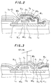
- Fig. 2 is a schematic cross-sectional view of a portion of a semiconductor memory cell according to Embodiment 1 of the present invention.
- Fig. 3 is a diagram showing a modified example of Embodiment 1.
- Fig. 4 is a diagram showing the principle of operation of a semiconductor memory cell according to a preferred mode of the first aspect of the invention.
- Fig. 5 is a schematic cross-sectional view of a portion of a semiconductor memory cell according to Embodiment 2 of the present invention.
- Fig. 6 is a diagram showing a modified example of Embodiment 2.
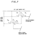
- Fig. 7 is a diagram showing the principle of operation of a semiconductor memory cell according to a second aspect of the present invention.
- Fig. 8 is a schematic cross-sectional view of a portion of a semiconductor memory cell according to Embodiment 3 of the present invention.
- Fig. 9 is a diagram showing a modified example of Embodiment 3.
- Fig. 10 is a diagram showing the principle of operation of a semiconductor memory cell according to a preferred mode of the second aspect of the present invention.
- Fig. 11 is a schematic cross-sectional view of a portion of a semiconductor memory cell according to Embodiment 4 of the present invention.
- Fig. 12 shows the principle of operation of a semiconductor memory cell according to a third aspect of the present invention along with schematic cross-sectional views showing a portion thereof.
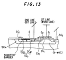
- Fig. 13 is a schematic cross-sectional view of a portion of a semiconductor memory cell according to a modified example of the third aspect of the present invention.
- Fig. 14 shows the principle of operation of a semiconductor memory cell according to a fourth aspect of the present invention along with schematic cross-sectional views showing a portion thereof.
- Fig. 15 shows the principle of operation of a semiconductor memory cell according to a fifth aspect of the present invention along with a schematic cross-sectional view showing a portion thereof.
- Fig. 16 shows the principle of operation of a semiconductor memory cell according to a sixth aspect of the present invention along with schematic cross-sectional views showing a portion thereof.
- Fig. 17 is a conceptual diagram showing a prior art one-transistor memory cell.
- Fig. 18 is a cross-sectional view of a memory cell having a prior art trench capacitor cell structure.
- Embodiment 1 is concerned with a semiconductor memory cell according to a first aspect of the invention.
- the semiconductor memory cell the principle of operation of which is shown in Fig. 1 and cross sections of a portion of which are shown schematically in Figs. 2 and 3, comprises an information storage transistor TR1 and a switching transistor TR2.
- the information storage transistor TR1 comprises a semiconductor channel layer Ch1, a first conductive gate G1, a second conductive gate G2, and first and second conductive layers, L1 and L2, each connected to either end of the semiconductor channel layer Ch1.
- the switching transistor TR2 comprises a semiconductor channel forming region Ch2, a third conductive gate G3, and third and fourth conductive layers, L3 and L4, each formed in the surface area of the semiconductor channel forming region Ch2 in contacting relationship forming a rectifier junction therewith.
- the third conductive gate G3 is formed in such a manner as to bridge the third conductive layer L3 and the fourth conductive layer L4.
- the semiconductor channel layer Ch1 has two opposing principal surfaces, the first principal surface MS1 and the second principal surface MS2.
- the first conductive gate G1 is formed opposite the principal surface MS1 of the semiconductor channel layer with a first barrier layer BL1 interposed therebetween.
- the second conductive gate G2 is formed opposite the principal surface MS2 of the semiconductor channel layer with a second barrier layer BL2 interposed therebetween.
- the semiconductor channel forming region Ch2 has a third principal surface MS3.
- the third conductive gate G3 is formed opposite the third principal surface MS3 of the semiconductor channel forming region Ch2 with a third barrier layer BL3 interposed therebetween.
- the fourth conductive layer L4 is connected to the second conductive gate G2.
- the first conductive gate G1 and the third conductive gate G3 are connected to a first memory-cell-selection line (for example, a word line).
- the first conductive gate G1 and the third conductive gate G3 are common.
- the first conductive layer L1 and the third conductive layer L3 are connected to a second memory-cell-selection line (for example, a bit line).
- the second conductive layer L2 is connected to a fixed potential including zero potential.
- the semiconductor channel forming region Ch2 is connected to a read/write selection line.
- the read/write selection line may be a common well or a substrate. In Embodiment 1, a common well is used.
- the second memory-cell-selection line (for example, a bit line) need not be provided more than one, and the chip area can be reduced.
- the conductive layers may be formed from a low-resistivity semiconductor, a silicide, a two-layered structure of silicide and semiconductor, a metal or the like.
- the barrier layers serve as barriers to channel carriers, and may be formed from an insulating material or a wide-gap semiconductor material.
- the information storage transistor TR1 has an SOI structure. That is, with the multilayered structure shown in Fig. 2, the total area that the information storage transistor and the switching transistor take up can be made approximately equal to the area that one transistor takes up, thus allowing the chip area to be reduced.
- the operation of the semiconductor memory cell will be described below, taking for example a case in which the information storage transistor TR1 and the switching transistor TR2 are both n-type transistors.
- First memory-cell-selection line e.g., word line
- Second memory-cell-selection line e.g., bit line
- 0 write
- V0 write
- V1 Read/write selection line
- V B_W Potentials applied to the various lines for a memory read are designated as follows. Note that during a read cycle, the read/write selection line is reverse biased.
- First memory-cell-selection line (e.g., word line) : V R Read/write selection line : V B_R
- the fixed potential to which the second conductive layer L2 is connected is designated as follows: Fixed potential to which the second conductive layer L2 is connected : V2
- the threshold voltages of the information storage transistor TR1 required at the first conductive gate G1 for memory read/write operations are designated as follows: "0" read/write : V TH1_0 "1" read/write : V TH1_1
- the potential of the second conductive gate G2 is different between a "0" read/write and a "1" read/write.
- the threshold voltage of the information storage transistor TR1 required at the first conductive gate G1 differs between a "0" read/write and a "1" read/write.
- the information storage transistor TR1 is provided with two conductive gates, G1 and G2, on opposite sides of the semiconductor channel layer Ch1; this structure serves to stabilize the operation of the information storage transistor TR1, and facilitates short-channel design. Furthermore, a capacitor having as large capacitance as required in prior art DRAMs is not required.
- the threshold voltage of the switching transistor TR2 required at the third conductive gate G3 for a write operation is designated as V TH2_W . Further, the threshold voltage of the switching transistor TR2 required at the third conductive gate G3 for a read operation is designated as V TH2_R .
- the threshold voltage of the switching transistor TR2 required at the third conductive gate G3 is different between memory write and memory read because the potential applied to the read/write selection line differs between write and read operations.
- the potential of the first line is V W . Therefore, the potential at the third conductive gate G3 of the switching transistor TR2 is also V W . Since the potential of the read/write selection line is V B_W , the threshold voltage, V TH2_W , of the switching transistor TR2 required at the third conductive gate has the following relationship with respect to V W . ⁇ V W ⁇ > ⁇ V TH2_W ⁇ As a result, the switching transistor TR2 is ON. Therefore, the potential at the second conductive gate G2 of the information transistor TR1 is V0 (when writing information "0") or V1 (when writing information "1").
- the potential at the first conductive gate G1 of the information storage transistor TR1 is V W .
- the threshold voltage of the information storage transistor TR1 required at the first conductive gate G1 is V TH1_0 or V TH1_1 . If the relationship ⁇ V W ⁇ > ⁇ V TH1_0 ⁇ > ⁇ V TH1_1 ⁇ exists between these potentials, the information storage transistor TR1 is also ON, but writing is performed whether the information storage transistor TR1 is ON or OFF.
- the potential at the second conductive gate G2 of the information storage transistor TR1 is V0 or V1. That is, the second conductive gate G2 is held at a potential corresponding to the information "0" or “1”, and this condition is substantially maintained within a prescribed time until the information is read out.
- the various portions of the information storage transistor TR1 and the switching transistor TR2 are set at such potentials that neither transistor will conduct.
- V B_R is set so that the threshold voltage, V TH2_R , of the switching transistor TR2 required at the third conductive gate has the following relationship with respect to V R . ⁇ V TH2_R ⁇ > ⁇ V R ⁇ The switching transistor TR2 is thus held OFF.
- the potential at the first conductive gate G1 of the information storage transistor TR1 is V R .
- the threshold voltage of the information storage transistor TR1 at the first conductive gate G1 is V TH1_0 or V TH1_1 .
- the threshold voltage of the information storage transistor TR1 is dependent on the potential of the second conductive gate G2. The following relationship exists between these potentials. ⁇ V TH1_0 ⁇ > ⁇ V R ⁇ > ⁇ V TH1_1 ⁇ Therefore, when the stored information is "0", the information storage transistor TR1 is OFF. On the other hand, when the stored information is "1", the information storage transistor TR1 is ON.
- the information storage transistor TR1 is set to an ON or OFF condition, depending on the stored information. Therefore, when the stored information is "1", current flows to the second line; when the stored information is "0", no current but the leakage current flows to the second line. The stored information can be read in this manner by the information storage transistor TR1.
- Table 1 The above-described operating conditions of the information storage transistor TR1 and the switching transistor TR2 are summarized in Table 1.
- the potential values given in Table 1 are only illustrative examples, and each potential can take any value as long as it satisfies the above conditions.
- FIG. 3 A modified example of the semiconductor memory cell of Embodiment 1 illustrated in Fig. 2 is shown schematically in cross section in Fig. 3.
- the semiconductor memory cell shown in Fig. 2 the first conductive gate G1 and the third conductive gate G3 are common.
- the second conductive gate G2 and the fourth conductive layer L4 are common.
- the read/write selection line is formed from a well. While a slightly larger plan area is required as compared with the memory cell shown in Fig. 2, the memory cell shown in Fig. 3 have the advantages of relatively smooth surface topography, which is advantageous in lithography, and a less number of contacts.
- Embodiment 2 is concerned with a preferred mode of the semiconductor memory according to the first aspect of the invention.
- the semiconductor memory cell the principle of operation of which is shown in Fig. 4 and cross sections of a portion of which are shown schematically in Figs. 5 and 6, comprises an information storage transistor TR1 and a switching transistor TR2.
- the structures of the information storage transistor TR1 and the switching transistor TR2 are fundamentally the same as those of Embodiment 1, except for the points hereinafter described.
- the information transistor TR1 is formed from a transistor of a first conductivity type, for example, a p-type transistor, and the switching transistor TR2 is formed from a transistor of the opposite conductivity type to that of the information storage transistor TR1, for example, an n-type transistor.
- the first conductive layer L1 and the second conductive layer L2 are formed from semiconductor material, then their conductivity type should be p type.
- the first conductive gate G1, the second conductive gate G2, the third conductive gate G3, the third conductive layer L3, and the fourth conductive layer L4 are formed from semiconductor material, then their conductivity type should be n+ type.
- these regions may be formed from a silicide, a two-layer structure of silicide and semiconductor, or a metal.
- the semiconductor channel forming region Ch2 is connected to a second fixed potential including zero potential.
- the first conductive layer L1 is connected to the second line via a fifth conductive layer L5 which forms a rectifier junction with the first conductive layer.
- the provision of the fifth conductive layer serves to prevent without fail a current from flowing into the information storage transistor TR1 during the writing of information. Furthermore, there is no possibility of the information write voltage being applied to the information storage transistor TR1 and thereby interfering with the write operation as was the case with the prior art.
- the potentials of the information storage transistor TR1 and the switching transistor TR2 are set to satisfy the following relationships. ⁇ V W ⁇ > ⁇ V TH2_W ⁇ ⁇ V TH1_1 ⁇ > ⁇ V R ⁇ > ⁇ V TH1_0 ⁇
- the potential of the first line is V W (>0). Therefore, the potential at the third conductive gate G3 of the switching transistor TR2 is also V W (>0). Since the second fixed potential is V B_W , if V W is set as ⁇ V W ⁇ > ⁇ V TH2_W + V0 or V1 ⁇ where V TH2_W is the threshold voltage of the switching transistor TR2 required at the third conductive gate G3, then the switching transistor TR2 is ON. Therefore, the potential at the second conductive gate G2 of the information transistor TR1 is V0 (when writing information "0") or V1 (when writing information "1").
- the potential at the first conductive gate G1 of the information storage transistor TR1 is V W (>0). Therefore, when V0 or V1 ⁇ V W - V TH1_1 , the information storage transistor TR1 is OFF. Even if it is ON, current flow is blocked by the presence of the rectifier junction between the first conductive layer L1 and the fifth conductive layer L5.
- the potential at the second conductive gate G2 of the information storage transistor TR1 is V0 or V1. That is, the second conductive gate G2 is held at a potential corresponding to the information "0" or “1”, and this condition is substantially maintained until the information is read out.
- the various portions of the information storage transistor TR1 and the switching transistor TR2 are set at such potentials that neither transistor will conduct.
- the potential of the first line is V R ( ⁇ 0). Therefore, the potential at the third conductive gate G3 of the switching transistor TR2 is V R ( ⁇ 0), and the switching transistor TR2 remains OFF unless the potential of the second line is made more negative than V R - V TH2_R .
- the second line is set at a small potential and information is read by sensing the current.
- the potential at the first conductive gate G1 of the information storage transistor TR1 is V R ( ⁇ 0).
- the threshold voltage of the information storage transistor TR1 required at the first conductive gate G1 is V TH1_0 or V TH1_1 .
- the threshold voltage of the information storage transistor TR1 is dependent on the potential of the second conductive gate G2. The following relationship exists between these potentials. ⁇ V TH1_1 ⁇ > ⁇ V R ⁇ > ⁇ V TH1_0 ⁇ Therefore, when the stored information is "0", the information storage transistor TR1 is ON. On the other hand, when the stored information is "1", the information storage transistor TR1 is OFF.
- the information storage transistor TR1 is set to an ON or OFF condition, depending on the stored information.
- the second conductive layer L2 of the information storage transistor TR1 is connected to the fixed potential (V2); therefore, when the stored information is "0", current flows to the second line, and when the stored information is "1", current does not flow to the second line.
- the stored information can be read in this manner by the information storage transistor TR1.
- FIG. 5 A cross section of a portion of the semiconductor memory cell of Embodiment 2 is shown schematically in Fig. 5.
- the semiconductor memory cell of Embodiment 2 is fundamentally the same as the semiconductor memory cell shown in Fig. 2, except that the information storage transistor TR1 and the switching transistor TR2 are of different conductivity types and that the first conductive layer L1 is connected to the second line via the n-type fifth conductive layer L5 which forms a rectifier junction with the p-type first conductive layer L1.
- Table 2 summarizes the operating conditions of the semiconductor memory cell in which the information storage transistor TR1 is formed from a p-type transistor and the switching transistor TR2 is formed from an n-type transistor.
- FIG. 5 A modified example of the semiconductor memory cell illustrated in Fig. 5 is shown schematically in cross section in Fig. 6.
- the semiconductor memory cell shown is fundamentally the same as the semiconductor memory cell shown in Fig. 3, except that the information storage transistor TR1 and the switching transistor TR2 are of different conductivity types and that the first conductive layer L1 is connected to the second line via the n-type fifth conductive layer L5 which forms a rectifier junction with the p-type first conductive layer L1.
- Embodiment 3 is concerned with a semiconductor memory cell according to a second aspect of the invention.
- the semiconductor memory cell comprises an information storage transistor TR1 and a switching transistor TR2.
- the information storage transistor TR1 comprises a first semiconductor channel layer Ch1, a first conductive gate G1, a second conductive gate G2, and first and second conductive layers, L1 and L2, each connected to either end of the first semiconductor channel layer Ch1.
- the switching transistor TR2 comprises a second semiconductor channel layer Ch2, a third conductive gate G3, a fourth conductive gate G4, and third and fourth conductive layers, L3 and L4, each connected to either end of the second semiconductor channel layer Ch2.
- the information storage transistor TR1 and the switching transistor TR2 both have an SOI structure (including a structure in which the barrier layer is formed from a wide-gap semiconductor, for example, GaAlAs as compared with GaAs).
- the first semiconductor channel layer Ch1 has two opposing principal surfaces, the first principal surface MS1 and the second principal surface MS2.
- the first conductive gate G1 is formed opposite the principal surface MS1 of the first semiconductor channel layer with a first barrier layer BL1 interposed therebetween.
- the second conductive gate G2 is formed opposite the principal surface MS2 of the first semiconductor channel layer with a second barrier layer BL2 interposed therebetween.
- the second semiconductor channel layer Ch2 has two opposing principal surfaces, the third principal surface MS3 and the fourth principal surface MS4.
- the third conductive gate G3 is formed opposite the third principal surface MS3 of the second semiconductor channel layer Ch2 with a third barrier layer BL3 interposed therebetween.
- the fourth conductive gate G4 is formed opposite the fourth principal surface MS4 of the second semiconductor channel layer Ch2 with a third barrier layer BL4 interposed therebetween.
- the fourth conductive layer L4 is connected to the second conductive gate G2.
- the fourth conductive layer L4 and the second conductive gate G2 are common.
- the first conductive gate G1 and the third conductive gate G3 are connected to a first memory-cell-selection line (for example, a word line).
- the first conductive layer L1 and the third conductive layer L3 are connected to a second memory-cell-selection line (for example, a bit line).
- the second conductive layer L2 is connected to a fixed potential including zero potential.
- the fourth conductive gate G4 is connected to a read/write selection line.
- the semiconductor memory cell of Embodiment 3 is different from the semiconductor memory cell of Embodiment 1 in that the switching transistor TR2 has the fourth conductive gate G4. This serves to further stabilize the operation of the switching transistor TR2 and yet allows further miniaturization.
- FIG. 9 A modified example of the semiconductor memory cell of Embodiment 3 illustrated in Fig. 8 is shown schematically in cross section in Fig. 9.
- the second conductive gate G2 and the fourth conductive layer L4 are common.
- the first conductive gate G1 and the third conductive gate G3 are formed in the same substrate surface.
- the first conductive gate G1 and the third conductive gate G3 may be connected to each other. While a slightly larger plan area is required than that of the memory cell shown in Fig. 8, the memory cell shown in Fig.
- first semiconductor channel layer Ch1 and the second semiconductor channel layer Ch2 can be formed using a single high-quality semiconductor layer whereas two such layers are needed in the structure of the semiconductor memory cell shown in Fig. 8.
- first conductive gate G1 and the third conductive gate G3 can be made common.
- Embodiment 4 is concerned with a preferred mode of the semiconductor memory cell according to the second aspect of the invention.
- the semiconductor memory cell the principle of operation of which is shown in Fig. 10 and a cross section of a portion of which is shown schematically in Fig. 11, comprises an information storage transistor TR1 and a switching transistor TR2.
- the structures of the information storage transistor TR1 and the switching transistor TR2 are fundamentally the same as those of Embodiment 3, except for the points hereinafter described.
- the information transistor TR1 is formed from a transistor of a first conductivity type, for example, a p-type transistor, and the switching transistor TR2 is formed from a transistor of the opposite conductivity type to that of the information storage transistor TR1, for example, an n-type transistor.
- the first conductive layer L1 and the second conductive layer L2 are formed from semiconductor material, then their conductivity type should be p type.
- the first conductive gate G1, the second conductive gate G2, the third conductive gate G3, the fourth conductive gate G4, the third conductive layer L3, and the fourth conductive layer L4 are formed from semiconductor material, then their conductivity type should be n+ type.
- the fourth conductive gate G4 is connected to a second fixed potential including zero potential.
- first conductive layer L1 is connected to the second line via an n-type fifth conductive layer L5 which forms a rectifier junction with the p-type first conductive layer L1.
- FIG. 11 A cross section of a portion of the semiconductor memory cell of Embodiment 4 is shown schematically in Fig. 11.
- the semiconductor memory cell of Embodiment 3 is fundamentally the same as the semiconductor memory cell shown in Fig. 9, except that the first and second conductive layers, L1 and L2, are of different conductivity type and that the first conductive layer L1 is connected to the second line via the n+ fifth conductive layer L5 which forms a rectifier junction with the p-type first conductive layer L1.
- the fifth conductive layer L5 and the rectifier junction between the first conductive layer L1 and the fifth conductive layer L5 are shown in schematic form for simplicity. It will also be appreciated that the first conductive gate G1 and the third conductive gate G3 may be connected to each other.
- the operation of the semiconductor memory cell is the same as that described in Embodiment 2 (see Table 2), and therefore, detailed explanation thereof is not repeated here.
- Embodiment 5 is concerned with a semiconductor memory cell according to a third aspect of the invention.
- the semiconductor memory cell comprises an information storage transistor TR1 formed from a field-effect transistor of a first conductivity type (for example, n type) and a switching transistor TR2 formed from a field-effect transistor of a second conductivity type (for example, p type).
- the information storage transistor TR1 comprises a first channel forming region Ch1 of the second conductivity type, a first conductive gate G1 formed above the first semiconductor channel forming region Ch1 with a first barrier layer interposed therebetween, and first and second conductive regions, SC1 and SC2, separated by the first conductive gate G1.
- the first conductive gate G1 is formed in such a manner as to bridge the first conductive region SC1 and the second conductive region SC2.
- the switching transistor TR2 comprises a second semiconductor channel forming region Ch2 of the first conductivity type, a second conductive gate G2 formed above the second semiconductor channel forming region Ch2 with a second barrier layer interposed therebetween, a third conductive region SC3, and a fourth conductive region SC4.
- the second conductive gate G2 is formed in such a manner as to bridge the third conductive region SC3 and the fourth conductive region SC4.
- the conductive regions are the source and drain regions.
- the first and second conductive regions, SC1 and SC2 are each formed from a low-resistivity semiconductor of the opposite conductivity type to that of the first semiconductor channel forming region Ch1, or from a metal or a silicide that forms a rectifier junction with the first semiconductor channel forming region Ch1.
- the third and fourth conductive regions, SC3 and SC4 are each formed from a low-resistivity semiconductor of the opposite conductivity type to that of the second semiconductor channel forming region Ch2, or from a metal or a silicide that forms a rectifier junction with the second semiconductor channel forming region Ch2.
- the first conductive gate G1 of the storage transistor TR1 and the second conductive gate G2 of the switching transistor TR2 are connected to a first memory-cell-selection line (for example, a word line).
- the fourth conductive region SC4 of the switching transistor TR2 is connected to, or formed common with, the channel forming region Ch1 of the storage transistor TR1.
- the third conductive region SC3 of the switching transistor TR2 is connected to a second memory-cell-selection line (for example, a bit line).
- the first conductive region SC1 of the information storage transistor TR1 is connected to a read line.
- the second conductive region SC2 is connected to a fixed potential including zero potential.
- First memory-cell-selection line e.g., word line
- Second memory-cell-selection line e.g., bit line
- Read potential is designated as follows: First memory-cell-selection line (e.g., word line) : V R
- Read line potential V2
- the threshold voltages of the information storage transistor TR1 required at the first conductive gate G1 for read operations are designated as follows: "0" read : V TH1_0 "1” read : V TH1_1
- the potential of the channel forming region Ch1 is different between a "0" read and a "1" read.
- the threshold voltage of the information storage transistor TR1 required at the first conductive gate G1 differs between a "0" read and a "1" read.
- the structure does not require the provision of a large capacitor as required in the prior art DRAM shown in Fig. 17.
- the potential of the information storage transistor TR1 is set to satisfy the following relationship. ⁇ V TH1_1 ⁇ > ⁇ V R ⁇ > ⁇ V TH1_0 ⁇ The operation of the semiconductor memory cell of Embodiment 5 will be described below.
- the potential at the first conductive gate G1 of the information storage transistor TR1 is V W ( ⁇ 0). Therefore, the information storage transistor TR1 is OFF.
- the potential of the channel forming region Ch1 of the information storage transistor TR1 is V0 (when writing information "0") or V1 or V W - V TH2 (when writing information "1").
- This condition changes with time because of leakage currents (between the substrate and the semiconductor channel forming region Ch1 of the information storage transistor TR1, off currents of the switching transistor TR2, etc.), but is maintained within an allowable range until the information is read out.
- the various portions of the information storage transistor TR1 and the switching transistor TR2 are set at such potentials that neither transistor will conduct. Furthermore, the so-call refresh operation is performed before the change in the potential of the channel forming region Ch1 of the information storage transistor TR1 becomes large enough to cause errors in read operations.
- the potential of the first line is V R (>0).
- the potential at the second conductive gate G2 of the switching transistor TR2 is V R (>0), and the switching transistor TR2 is OFF.
- the potential at the first conductive gate G1 of the information storage transistor TR1 is V R (>0).
- the threshold voltage of the information storage transistor TR1 required at the first conductive gate G1 is V TH1_0 or V TH1_1 .
- the threshold voltage of the information storage transistor TR1 is dependent on the potential of the channel forming region Ch1. The following relationship exists between these threshold voltages. ⁇ V TH1_1 ⁇ > ⁇ V R ⁇ > ⁇ V TH1_0 ⁇ Therefore, when the stored information is "0", the information storage transistor TR1 is ON. On the other hand, when the stored information is "1", the information storage transistor TR1 is OFF.
- the information storage transistor TR1 is set to an ON or OFF condition, depending on the stored information. Since the first conductive region SC1 of the information storage transistor TR1 is connected to the read line or the second line, current flows or does not flow to the information storage transistor TR1, depending on the stored information ("0" or "1"). The stored information can be read out in this manner by the information storage transistor TR1. A mode in which the first conductive region SC1 of the information storage transistor TR1 is connected to the second line will be described hereinafter.
- Table 3 The above-described operating conditions of the information storage transistor TR1 and the switching transistor TR2 are summarized in Table 3.
- the potential values given in Table 3 are only illustrative examples, and each potential can take any value as long as it satisfies the above conditions.
- the read line may be formed common with the second line.
- the first conductive region SC1 is connected to the second line via a p-n junction or a Schottky junction type rectifying diode D2, as indicated by a dotted line in Fig. 12(B).
- This semiconductor memory cell structure can be realized, for example, in the structure shown in Fig. 12(C).
- the diode D2 is formed by forming the first conductive region SC1 from a semiconductor and forming the third conductive region SC3 in the surface area thereof, the conductivity type of the third conductive region SC3 being opposite to that of the first conductive region SC1.
- the first semiconductor channel forming region Ch1 and the fourth conductive region SC4 are formed of a common region.
- the first conductive region SC1 and the second semiconductor channel forming region Ch2 are formed of a common region.
- the readout voltage applied to the second line must be small enough that a large forward current will not flow across the junction between the first conductive region SC1 and the third conductive region SC3 (0.4 V or less in the case of a p-n junction); otherwise, latch-up may occur.
- One way to prevent the latch-up condition is to form the third conductive region SC3 from a silicide or a metal so that the third conductive region SC3 and the first conductive region SC1 form a junction such as a Schottky junction where majority carriers essentially form the forward current.
- the third conductive region SC3 may be formed, as shown in Fig. 13, for example, from a p-type semiconductor region SC 3P and a metal layer of Mo, Al, etc. or a silicide layer, SC 3S , that can form a Schottky junction with the first conductive region SC1.
- the first conductive gate G1 and the second conductive gate G2 are formed common.
- the reference sign E designates an electrode Al or Al/TiN/Ti triple layer formed on the third conductive region SC3, and the first conductive region SC1 is formed, for example, from an n-type semiconductor.
- this embodiment provides the structure that can also be employed in CMOS fabrication, and therefore, the structure, among others, the structure shown in Fig. 12(B), is particularly suitable for DRAMs integrated in CMOS ASICs.
- Embodiment 6 is concerned with a semiconductor memory cell according to a fourth aspect of the invention.
- the semiconductor memory cell of Embodiment 6 the principle of operation of which is shown in Fig. 14(A) and a cross section of a portion of which is shown schematically in Fig. 13(B), comprises an information storage transistor TR1 of a first conductivity type (for example, n type) and a switching transistor TR2 of a second conductivity type (for example, p type) opposite to the first conductivity type.
- the information storage transistor TR1 comprises a first conductive gate G1, first and second conductive regions, SC1 and SC2, formed, for example, from an n+ semiconductor, and a first semiconductor channel forming region Ch1 (common with a p-well in the example shown in Fig. 14(B)).
- the first conductive region SC1 and the second conductive region SC2 each form a rectifier junction with the surface area of the first semiconductor channel forming region Ch1.
- the first conductive gate G1 is formed opposite a first principal surface of the first semiconductor channel forming region Ch1, with a first barrier layer interposed therebetween, in such a manner as to bridge the first and second conductive regions SC1 and SC2.
- the switching transistor TR2 comprises a second conductive gate G2, third and fourth conductive regions, SC3 and SC4, formed, for example, from a p+ semiconductor, and a second semiconductor channel forming region Ch2.
- the third conductive region SC3 and the fourth conductive region SC4 are connected to the second semiconductor channel forming region Ch2.
- the second conductive gate G2 is formed opposite a second principal surface of the second semiconductor channel forming region Ch2 with a second barrier layer interposed therebetween.
- the first conductive gate G1 of the information storage transistor TR1 and the second conductive gate G2 of the switching transistor TR2 are connected to a first memory-cell-selection line (for example, a word line).
- the fourth conductive region SC4 of the switching transistor TR2 is connected to the channel forming region Ch1 of the information storage transistor TR1.
- the third conductive region SC3 of the switching transistor TR2 is connected to a second memory-cell-selection line (for example, a bit line).
- the second conductive region SC2 of the information storage transistor TR1 is connected to a fixed potential.
- the first conductive region SC1 of the information storage transistor TR1 is connected to the third conductive region SC3 of the switching transistor TR2, forming at their boundary a rectifier junction of p-n junction or Schottky junction type.
- the impurity concentration in the first conductive region SC1 at the junction adjusted to 2 x 1019cm ⁇ 3 or less, the dielectric strength or leakage current characteristic at the rectifier junction can be improved.
- First memory-cell-selection line e.g., word line
- Second memory-cell-selection line e.g., bit line
- "0" write V0 "1" write
- V1 Read potential is designated as follows: First memory-cell-selection line (e.g., word line) : V R
- Fixed potential V2
- the threshold voltages of the information storage transistor TR1 required at the first conductive gate G1 for read operations are designated as follows: "0" read : V TH1_0 "1” read : V TH1_1
- the potential of the channel forming region Ch1 is different between a "0" read and a "1" read.
- the threshold voltage of the information storage transistor TR1 required at the first conductive gate G1 differs between a "0" read and a "1" read.
- the structure does not require the provision of a large capacitor as required in the prior art DRAM.
- the potential of the information storage transistor TR1 is set to satisfy the following relationship. ⁇ V TH1_1 ⁇ > ⁇ V R ⁇ > ⁇ V TH1_0 ⁇ The operation of the semiconductor memory cell of Embodiment 6 will be described below.
- the potential at the first conductive gate G1 of the information storage transistor TR1 is V W ( ⁇ 0). Therefore, the information storage transistor TR1 is OFF.
- the potential of the channel forming region Ch1 of the information storage transistor TR1 is V0 (when writing information "0") or V1 or V W - V TH2 (when writing information "1").
- This condition changes with time because of leakage currents (between the substrate and the semiconductor channel forming region Ch1 of the information storage transistor TR1, off currents of the switching transistor TR2, etc.), but is maintained within an allowable range until the information is read out.
- the various portions of the information storage transistor TR1 and the switching transistor TR2 are set at such potentials that neither transistor will conduct. Furthermore, the so-call refresh operation is performed before the change in the potential of the channel forming region Ch1 of the information storage transistor TR1 becomes large enough to cause errors in read operations.
- the first conductive region SC1 of the information storage transistor TR1 is connected to the third conductive region SC3 of the switching transistor TR2, forming at their boundary a rectifier junction of p-n junction or Schottky junction type. This perfectly prevents the current flow to the first conductive region SC1 during the writing of information.
- the potential of the first line is V R (>0).
- the potential at the second conductive gate G2 of the switching transistor TR2 is V R (>0), and the switching transistor TR2 is OFF.
- the potential at the first conductive gate G1 of the information storage transistor TR1 is V R (>0).
- the threshold voltage of the information storage transistor TR1 required at the first conductive gate G1 is V TH1_0 or V TH1_1 .
- the threshold voltage of the information storage transistor TR1 is dependent on the potential of the channel forming region Ch1. The following relationship exists between these threshold voltages. ⁇ V TH1_1 ⁇ > ⁇ V R ⁇ > ⁇ V TH1_0 ⁇ Therefore, when the stored information is "0", the information storage transistor TR1 is ON. On the other hand, when the stored information is "1", the information storage transistor TR1 is OFF.
- the information storage transistor TR1 is set to an ON or OFF condition, depending on the stored information. Since the second conductive region SC2 of the information storage transistor TR1 is connected to the fixed potential, current flows or does not flow to the information storage transistor TR1, depending on the stored information ("0" or "1"). The stored information can be read out in this manner by the information storage transistor TR1.
- Table 4 The above-described operating conditions of the information storage transistor TR1 and the switching transistor TR2 are summarized in Table 4.
- the potential values given in Table 4 are only illustrative examples, and each potential can take any value as long as it satisfies the above conditions.
- Fig. 14(C) shows a modified example of the semiconductor memory cell of Embodiment 6.
- an auxiliary gate (a third conductive gate) G3 is formed opposite the second conductive gate G2 and facing a third principal surface of the second semiconductor channel forming region Ch2 with a third barrier layer interposed therebetween.
- the auxiliary gate G3 has the function of shielding the semiconductor forming region Ch2 from potentials induced at and ions adhering to the surface of the semiconductor memory cell, thereby ensuring stable operation of the semiconductor memory cell.
- the auxiliary gate G3 to the read/write selection line, read or write operating margins can be improved.
- the semiconductor memory cell thus constructed has further improved characteristics as compared with the semiconductor memory cell whose principle of operation is shown in Fig. 4.
- Embodiment 7 is concerned with a semiconductor memory cell according to a fifth aspect of the invention.
- first semiconductor region SC1 of a first conductivity type for example, n type
- first conductive region SC2 formed from a material of a second conductivity type opposite to the first conductivity type (for example, p+) or from other material such as a metal or a silicide that forms a rectifier junction with the first semiconductor region SC1
- second semiconductor region SC3 of the second conductivity type for example, p+ type
- second conductive region SC4 formed from a material of the first conductivity type (for example, n+) or from other material such as a metal or a silicide that forms a rectifier junction with the second semiconductor region SC3
- a conductive gate G disposed in such a manner as to form a bridge over a barrier layer between the first semiconductor region SC1 and the second conductive region SC4 and between the first conductive region SC2 and the second semiconductor region SC3.
- the first semiconductor region SC1 is formed in the surface area of a semiconductor substrate or on an insulating substrate.
- the first conductive region SC2 is formed in the surface area of the first semiconductor region SC1.
- the second semiconductor region SC3 is formed in the surface area of the first semiconductor region SC1 but spaced apart from the first conductive region SC2.
- the second conductive region SC4 is formed in the surface area of the second semiconductor region SC3.
- the conductive gate G is connected to a first memory-cell-selection line (for example, a word line).
- the first conductive region SC2 is connected to a write information setting line.
- the second conductive region SC4 is connected to a second memory-cell-selection line (for example, a bit line).
- the first semiconductor region SC1 (corresponding to the channel forming region Ch2), the first conductive region SC2 (corresponding to a source/drain region), the second semiconductor region SC3 (corresponding to a source/drain region), and the conductive gate G constitute the switching transistor TR2.
- the second semiconductor region SC3 (the surface area below the conductive gate G corresponds to the channel forming region Ch1(p)), the first semiconductor region SC1 (corresponding to a source/drain region), the second conductive region SC4 (corresponding to a source/drain region), and the conductive gate G constitute the information storage transistor TR1.
- First memory-cell-selection line e.g., word line
- First memory-cell-selection line e.g., word line
- V R the potential of the second memory-cell-selection line (for example, bit line) to which the second conductive region SC4 is connected
- Second memory-cell-selection line V2
- the threshold voltages of the information storage transistor TR1 required at the conductive gate G for read operations are designated as follows: “0" read : V TH1_0 "1" read : V TH1_1
- the potential of the channel forming region Ch1 is different between a "0” read and a "1” read.
- the threshold voltage of the information storage transistor TR1 at the conductive gate G differs between a "0” read and a "1” read.
- the structure does not require the provision of a large capacitor as required in the prior art DRAM.
- the potential of the information storage transistor TR1 is set to satisfy the following relationship. ⁇ V TH1_1 ⁇ > ⁇ V R ⁇ > ⁇ V TH1_0 ⁇ The operation of the semiconductor memory cell of Embodiment 7 will be described below.
- the various portions of the information storage transistor TR1 and the switching transistor TR2 are set at such potentials that neither transistor will conduct.
- the potential of the first line should be set at 0 (V) and the potential of the second line at V1, for example.
- the potential at the conductive gate G of the information storage transistor TR1 is V W ( ⁇ 0). Therefore, the information storage transistor TR1 is OFF.
- the potential of the channel forming region Ch1 of the information storage transistor TR1 is V0 (when writing information "0") or V1 or V W - V TH2 (when writing information "1").
- This condition changes with time because of leakage currents (between the first semiconductor region SC1 and the semiconductor channel forming region Ch1 of the information storage transistor TR1, off currents of the switching transistor TR2, etc.), but is maintained within an allowable range until the information is read out.
- the so-call refresh operation is performed before the change in the potential of the channel forming region Ch1 of the information storage transistor TR1 becomes large enough to cause errors in read operations.
- the potential of the first line is V R (>0).
- the potential at the conductive gate G of the switching transistor TR2 is V R (>0), and the switching transistor TR2 is OFF.
- the potential at the conductive gate G of the information storage transistor TR1 is V R (>0).
- the threshold voltage of the information storage transistor TR1 required at the conductive gate G is V TH1_0 or V TH1_1 .
- the threshold voltage of the information storage transistor TR1 is dependent on the potential of the channel forming region Ch1. The following relationship exists between these potentials. ⁇ V TH1_1 ⁇ > ⁇ V R ⁇ > ⁇ V TH1_0 ⁇ Therefore, when the stored information is "0", the information storage transistor TR1 is ON. On the other hand, when the stored information is "1", the information storage transistor TR1 is OFF.
- the information storage transistor TR1 is set to an ON or OFF condition, depending on the stored information. Since the second conductive region SC4 is connected to the second line, current flows or does not flow to the information storage transistor TR1, depending on the stored information ("0" or "1"). The stored information can be read out in this manner by the information storage transistor TR1.
- Table 5 The above-described operating conditions of the information storage transistor TR1 and the switching transistor TR2 are summarized in Table 5.
- the potential values given in Table 5 are only illustrative examples, and each potential can take any value as long as it satisfies the above conditions.
- Embodiment 8 is concerned with a semiconductor memory cell according to a sixth aspect of the invention.
- the semiconductor memory cell of Embodiment 8 the principle of operation of which is shown in Fig. 16(A) and a cross section of a portion of which is shown schematically in Fig.
- first semiconductor region SC1 of a first conductivity type for example, n type
- first conductive region SC2 formed from a material of a second conductivity type opposite to the first conductivity type (for example, p+) or from other material such as a metal or a silicide that forms a rectifier junction with the first semiconductor region SC1)
- second semiconductor region SC3 of the second conductivity type for example, p+ type
- second conductive region SC4 formed from a material of the first conductivity type (for example, n+) or from other material such as a metal or a silicide that forms a rectifier junction with the second semiconductor region SC3)
- a conductive gate G formed in such a manner as to bridge the second conductive region SC4 and a portion of the first semiconductor region SC1 flanked by the second semiconductor region SC3 and the first conductive region SC2 and also bridge the first conductive region SC2 and the second semiconductor region SC3.
- the semiconductor memory cell shown in Fig. 16(B) is depicted in more detail in Fig. 16(C).
- part of the structure of the semiconductor memory cell structure shown in Fig. 16(C) can be applied to the structure shown in Fig. 15(B).
- the first semiconductor region SC1 is formed on a semiconductor substrate as an isolated region in the surface area thereof, or on an insulating substrate as a region attached to a support substrate with an insulating layer such as an SiO2 layer interposed therebetween.
- the first conductive region SC2 is formed in the surface area of the first semiconductor region SC1.
- the second semiconductor region SC3 is formed in the surface area of the first semiconductor region SC1 but spaced apart from the first conductive region SC2.
- the second conductive region SC4 is formed in the surface area of the second semiconductor region SC3.
- the conductive gate G is connected to a first-memory-cell selection line (for example, a word line).
- the first semiconductor region SC1 is connected to a second memory-cell-selection line (for example, a bit line).
- the first conductive region SC2 is connected to a first fixed potential.
- the second conductive region SC4 is connected to a second fixed potential.
- the first semiconductor region SC1 (corresponding to the channel forming region Ch2), the first conductive region SC2 (corresponding to a source/drain region), the second semiconductor region SC3 (corresponding to a source/drain region), and the conductive gate G constitute the switching transistor TR2.
- the second semiconductor region SC3 (the surface area below the conductive gate G corresponds to the channel forming region Ch1(p)), the first semiconductor region SC1 (corresponding to a source/drain region), the second conductive region SC4 (corresponding to a source/drain region), and the conductive gate G constitute the information storage transistor TR1.
- the first fixed potential to which the first conductive region SC2 is connected is designated as V3 ( ⁇ 0).
- the second fixed potential to which the second conductive region SC4 is connected is designated as V4 ( ⁇ 0).
- First memory-cell-selection line e.g., word line
- Second memory-cell-selection line e.g., bit line
- the threshold voltages of the switching transistor TR2 required at the conductive gate for write operations are designated as follows: "0" write : V TH2W_0 "1" write : V TH2W_1
- Read potential is designated as follows: First memory-cell-selection line (e.g., word line) : V R
- the threshold voltages of the information storage transistor TR1 required at the conductive gate G for read operations are designated as follows: “0” read : V TH1R_0 "1” read : V TH1R_1
- the potentials of the channel forming regions Ch1 and Ch2 are different between a "0" read/write and a "1" read/write.
- the threshold voltages of the information storage transistor TR1 and the switching transistor TR2 required at the conductive gate G differ between a "0" read/write and a "1" read/write.
- the structure does not require the provision of a large capacitor as required in the prior art DRAM.
- the potential at the conductive gate of the switching transistor TR2, relative to V W is set as shown below, for example, for simplicity of explanation.
- the potential at the conductive gate of the information storage transistor TR1, relative to V R is set as follows: ⁇ V TH1_1 ⁇ > ⁇ V R ⁇ > ⁇ V TH1_0 ⁇
- the operation of the semiconductor memory cell of Embodiment 8 will be described below.
- the potential of the first line is set at V W ( ⁇ 0).
- the potential at the conductive gate G of the switching transistor TR2 is also V W ( ⁇ 0).
- V W is ⁇ V W ⁇ > ⁇ V TH2W_1 ⁇ or ⁇ V TH2W_0 ⁇ whichever larger Therefore, for a write operation, the switching transistor TR2 is ON. Consequently, the potential of the channel forming region Ch1 of the information storage transistor TR1 is "0" information write : V3 "1" information write : V3
- the potential at the conductive gate G of the information storage transistor TR1 is V W ( ⁇ 0).
- the information storage transistor TR1 is OFF.
- the potential of the channel forming region Ch1 of the information storage transistor TR1 is V3 for both "0" and "1" information write.
- the second line potential at this time is denoted by V5 ( ⁇ V5 ⁇ ⁇ ⁇ V0 ⁇ or ⁇ V1 ⁇ )
- the potential of the first semiconductor channel Ch1 is ⁇ V3 - (V0 - V5) ⁇ or ⁇ V3 - (V1 - V5) ⁇
- ⁇ is the ratio of the capacitance between the first semiconductor region SC1 and the second semiconductor region SC3 to the total capacitance between the second semiconductor region SC3 and the other areas (including the first semiconductor region SC1) than the second semiconductor region SC3.
- This condition changes with time because of leakage currents (between the first semiconductor region SC1 and the semiconductor channel forming region Ch1 of the information storage transistor TR1, off currents of the switching transistor TR2, etc.), but is maintained within an allowable
- the various portions of the information storage transistor TR1 and the switching transistor TR2 are set at such potentials that neither transistor will conduct.
- the potential of the first line should be set at 0 (V) and the potential of the second line at V5, for example.
- the so-called refresh operation is performed before the change in the potential of the channel forming region Ch1 of the information storage transistor TR1 becomes large enough to cause errors in read operations.
- the potential of the first line is V R (>0), and the potential of the second line is V6 ( ⁇ V6 ⁇ ⁇ ⁇ V0 ⁇ or ⁇ V1 ⁇ ).
- the potential at the conductive gate G of the switching transistor TR2 is V R (>0), and the switching transistor TR2 is OFF.
- the potential at the conductive gate G of the information storage transistor TR1 is V R (>0).
- the threshold voltage of the information storage transistor TR1 required at the first conductive gate G1 is V TH1R_0 or V TH1R_1 which is given by the potential between the second semiconductor region SC3 and the second conductive region SC4 when ⁇ V3 - (V0 - V6) ⁇ or ⁇ V3 - (V1 - V6) ⁇ is met.
- the threshold voltage of the information storage transistor TR1 is dependent on the potential of the channel forming region Ch1. The following relationship exists between these potentials.
- the information storage transistor TR1 is set to an ON or OFF condition, depending on the stored information. Since the second conductive region SC4 is connected to the second fixed potential, current flows or does not flow to the information storage transistor TR1, depending on the stored information ("0" or "1"). The stored information can be read out in this manner by the information storage transistor TR1.
- the semiconductor memory cell of the invention has been described above in accordance with preferred embodiments, but it will be appreciated that the invention is not limited to those described preferred embodiments.
- the information storage transistor TR1 and the switching transistor TR1 may be both formed from p-type transistors.
- the information storage transistor TR1 may be formed from an n-type transistor and the switching transistor TR2 from a p-type transistor.
- the information storage transistor TR1 may be formed from a p-type transistor and the switching transistor TR2 from an n-type transistor. It will also be appreciated that the arrangement of elements in each transistor shown is only illustrative and may be modified as needed.
- the present invention is applicable not only to memory cells formed from silicon semiconductors but also to memory cells formed from compound semiconductors such as GaAs, for example.
- the operation of the information storage transistor is determined in depending relationship on the potential or charge (information) stored on the second conductive gate or in the channel forming region of the information storage transistor, and the information read out as the transistor current during refresh intervals is independent of the magnitude of the capacitance of a capacitor (for example, the capacitance of the second conductive gate plus added capacitance, etc.) if such a capacitor is added.
- a capacitor for example, the capacitance of the second conductive gate plus added capacitance, etc.
- the maximum area of the semiconductor memory cell is equal to or smaller than the area of two transistors.
- a conductive gate is provided opposite each of two principal surfaces of the semiconductor channel layer of the information storage transistor.
- This structure eliminates the problem of unstable transistor operation inherent in prior art transistor structures; that is, the structure of the invention is effective in stabilizing the operation of the information storage transistor, and facilitates short-channel transistor design.
- the first conductive gate and the third conductive gate are both connected to the first memory-cell-selection line. Accordingly, the first memory-cell-selection line need not be provided more than one, and the chip area can be reduced. Furthermore, depending on the structure, it is possible to form a memory cell within an area equal to one transistor area.
- a fourth gate is provided as an extra gate of the switching transistor. The provision of this extra gate serves to further stabilize the operation of the switching transistor.
- a fifth conductive layer is provided.
- the provision of this fifth conductive layer prevents without fail a current from flowing to the information storage transistor during the information write operation.
- the semiconductor memory cell fabrication process according to the third aspect of the invention is compatible with the fabrication process for CMOS ASICs, as shown, for example, in Fig. 12(B).
- the process therefore allows DRAM functions to be incorporated in an ASIC without requiring extra processing steps although the semiconductor memory cell area increases slightly.
- the semiconductor memory cell structure shown in Fig. 12(C) for example, one extra processing step may be required as compared to the CMOS ASIC structure, but the semiconductor memory cell area can be reduced nearly by half.
- the semiconductor memory cell can be implemented on an area approximately equal to one transistor area.
- the semiconductor memory cell can be implemented on an area approximately equal to one transistor area by using conventional semiconductor memory cell fabrication techniques without relying on SOI technology.
Landscapes
- Engineering & Computer Science (AREA)
- Microelectronics & Electronic Packaging (AREA)
- Computer Hardware Design (AREA)
- Power Engineering (AREA)
- Physics & Mathematics (AREA)
- Condensed Matter Physics & Semiconductors (AREA)
- General Physics & Mathematics (AREA)
- Semiconductor Memories (AREA)
- Dram (AREA)
- Thin Film Transistor (AREA)
- Metal-Oxide And Bipolar Metal-Oxide Semiconductor Integrated Circuits (AREA)
Abstract
Description
- The present invention relates to a semiconductor memory cell consisting of two transistors or one transistor formed by combining two transistors.
- Fig. 17 shows a conventional dynamic memory cell consisting of a single transistor and a capacitor; the memory cell of this structure is generally known as a one-transistor memory cell and used as a semiconductor memory cell suitable for high density devices. In such a memory cell, the capacitance of the capacitor needs to be high enough to cause a voltage change on the associated bit line. However, the trend to smaller plan area of the semiconductor memory cell necessitates a reduction in the size of the capacitor formed in a horizontal plate-like shape, giving rise to the problem that when reading information stored as a charge on the memory cell capacitor, the information is masked by noise, or that, because of increasing stray capacitance on the bit line with each generation of memory cells, only a small voltage change can be caused to the bit line. In one approach to solving this problem, there is proposed a dynamic memory cell having a trench capacitor cell structure (see Fig. 18) or a stacked capacitor cell structure. However, because of processing limitations on how deep the trench can be formed and how high the stack (stacked layers) can be made, there is a limit to increasing the capacitance of the capacitor. Accordingly, it is said that dynamic memory cells of these structures encounter the limit of miniaturization in the dimensional region beyond the low submicron rule.
- Furthermore, with transistors forming the semiconductor memory cells, reducing the transistor's plan area beyond the low submicron rule would introduce such problems as dielectric strength degradation, punch-through, etc., which would increase the possibility of leakage even under the rated voltage condition. With conventional transistor structures, therefore, it becomes difficult to ensure proper operation of the memory cell when the memory cell size is reduced.
- To overcome the above limitations on the capacitance, there is proposed a memory cell structure wherein the memory cell is constructed with two transistors and the transistor channel current is sensed.
- In the memory cell disclosed in Japanese Patent Unexamined Publication No. 63-19847, for example, a capacitor C₂ coupled to the gate and drain of a MOS transistor Q₁ is connected to a word line, as shown in Fig. 3 accompanying the same Patent Publication. Furthermore, the drain of the transistor Q₁ is connected to the gate of an SOI transistor Q₂ of the complementary type to the transistor Q₁. The drain of the transistor Q₂ is in turn connected to a fixed potential VD, while the source of each of the transistors, Q₁ and Q₂, is connected to a bit line.
- In the memory cell disclosed in the above Patent Publication, since the gate electrode of the SOI (silicon-on-insulator) transistor Q₂ is formed only on one principal surface side of the channel region thereof having two principal surfaces, an extra capacitor C₂ is needed to complete the structure of the memory cell. A further problem is that because of the charge or electric field applied (through an insulating film) to the other principal surface of the channel region of the SOI transistor Q₂, the operation of the SOI transistor Q₂ becomes unstable and it is difficult to reduce the channel length.
- On the other hand, the memory cell disclosed in Japanese Patent Unexamined Publication No. 1-145850 is constructed with a write transistor 18, a read transistor 19 (an SOI transistor), and a protective capacitor 20, as shown in Fig. 1 accompanying the same Patent Publication. The source of the write transistor 18 is connected to the gate of the read transistor 19. The cathode of the protective diode 20 is connected to the drain of the read transistor 19. Further, the anode of the protective diode 20 and the drain of the write transistor 18 are connected to a bit line, while the source of the read transistor 19 and the gate of the write transistor 18 are connected to a word line.
- In the memory cell disclosed in the above Patent Publication, since the read transistor 19 is an SOI transistor, when the source potential is caused to change to the same polarity as the gate potential (when writing a "1") the potential of the channel region changes with the change of the gate potential, resulting in an incomplete writing condition. It is therefore difficult to read the "1" with the expected certainty. Furthermore, in the read transistor 19, the gate electrode is formed only on one principal surface side of the channel region having two principal surfaces. Therefore, this structure also has the problem that because of the charge or electric field applied (through an insulating film) to the other principal surface side of the channel region of the read transistor 19, the operation of the read transistor 19 becomes unstable and it is difficult to reduce the channel length.
- The memory cells disclosed in Japanese Patent Unexamined Publication Nos. 62-141693 and 62-254462 each comprise a write transistor T1, a read transistor T2, and a storage capacitor C, as shown in Fig. 1 accompanying the former Patent Publication. The drains of the transistors T1 and T2 are connected to a bit line, and the source of the transistor T1 is connected to the storage capacitor and also to a first gate of the transistor T2. Further, the gate of the transistor T1 is connected to a write selection line, while a second gate (or a channel forming region such as a well) of the transistor T2 is connected to a read selection line.
- When the read transistor T2 is formed from an SOI transistor, the first and second gates are respectively formed on the upper and lower surface sides of the channel region of the transistor T2 (refer to Japanese Patent Application No. 55-93521 and Japanese Patent Unexamined Publication No. 57-18364). This structure eliminates the problem that has placed a limitation on the reduction of the channel length. For the write transistor T1, on the other hand, only bulk-type transistors are disclosed as preferred embodiments, and therefore, there is a limit to the miniaturization of the memory cell as a whole. Furthermore, the structure requiring each word line to be divided into a read line and a write line has the problem of increased chip area or increased number of stacked layers.
- The present invention is concerned with the structure of a memory cell constructed with two transistors and yet capable of solving the above enumerated problems. An object of the invention is to provide a semiconductor memory cell, a semiconductor memory cell for ASICs (Application Specific Integrated Circuits), and even a semiconductor memory cell with a single transistor formed by combining two transistors, of the structure that ensures stable transistor operation, that does not require the provision of a large-capacitance capacitor as required in prior art DRAMs, and that allows the channel length to be reduced and achieves miniaturization of the cell.
- To achieve the above object, in accordance with a first aspect of the invention, there is provided a semiconductor memory cell, as shown in the schematic diagram of Fig. 1, comprising:
an information storage transistor TR₁ comprising a semiconductor channel layer Ch₁ having first and second opposing principal surfaces; first and second conductive gates, G₁ and G₂, respectively disposed opposite the two principal surfaces of the semiconductor channel layer Ch₁ with first and second barrier layer respectively interposed therebetween; and first and second conductive regions, L₁ and L₂, respectively connected to either end of the semiconductor channel layer Ch₁, and
a switching transistor TR₂ comprising a semiconductor channel forming region Ch₂ having a third principal surface; a third conductive gate G₃ disposed opposite the third principal surface of the semiconductor channel forming region Ch₂ with a third barrier layer interposed therebetween; and third and fourth conductive layers, L₂ and L₄, each formed in a surface region of the semiconductor channel forming region Ch₂ and near either end of the third conductive gate G₃, wherein
the fourth conductive layer L₄ is connected to the second conductive gate G₂,
the first conductive gate G₁ and the third conductive gate G₃ are connected to a first memory-cell-selection line,
the first conductive layer L₁ and the third conductive layer L₃ are connected to a second memory-cell-selection line,
the second conductive layer L₂ is connected to a fixed potential including zero potential, and
the semiconductor channel forming region Ch₂ is connected to a read/write selection line. - In the above structure, the conductive layers may be formed from a low-resistivity semiconductor, a silicide, a two-layered structure of silicide and semiconductor, a metal, or the like. The barrier layers serve as barriers to channel carriers, and may be formed from an insulating material or a wide-gap semiconductor material.
- In one preferred mode of the semiconductor memory cell according to the first aspect of the invention, as shown in the schematic diagram of Fig. 4,
the information storage transistor TR₁ is formed from a transistor of a first conductivity type,
the switching transistor TR₂ is formed from a transistor of a conductivity type opposite to the first conductivity type,
the first conductive layer L₁ is connected to the second line via a fifth conductive layer L₅ which forms a rectifier junction with the first conductive layer L₁, and
the semiconductor channel forming region Ch₂ is connected to a second fixed potential including zero potential. - To achieve the above object, in accordance with a second aspect of the invention, there is provided a semiconductor memory cell, as shown in the schematic diagram of Fig. 7, comprising:
an information storage transistor TR₁ comprising a first semiconductor channel layer Ch₁ having first and second opposing principal surfaces; first and second conductive gates, G₁ and G₂, respectively disposed opposite the two principal surfaces of the first semiconductor channel layer Ch₁ with first and second barrier layers respectively interposed therebetween; and first and second conductive regions, L₁ and L₂, each connected to either end of the first semiconductor channel layer Ch₁, and
a switching transistor TR₂ comprising a second semiconductor channel layer Ch₂ having third and fourth opposing principal surfaces; third and fourth conductive gates, G₃ and G₄, respectively disposed opposite the two principal surfaces of the second semiconductor channel layer Ch₂ with third and fourth barrier layers respectively interposed therebetween; and third and fourth conductive layers, L₃ and L₄, each connected to either end of the second semiconductor channel region Ch₂, wherein
the fourth conductive layer L₄ is connected to the second conductive gate G₂,
the first conductive gate G₁ and the third conductive gate G₃ are connected to a first memory-cell-selection line,
the first conductive layer L₁ and the third conductive layer L₃ are connected to a second memory-cell-selection line,
the second conductive layer L₂ is connected to a fixed potential including zero potential, and
the fourth conductive gate G₄ is connected to a read/write selection line. - In one preferred mode of the semiconductor memory cell according to the second aspect of the invention, as shown in the schematic diagram of Fig. 10,
the information storage transistor TR₁ is formed from a transistor of a first conductivity type,
the switching transistor TR₂ is formed from a transistor of a conductivity type opposite to the first conductivity type,
the first conductive layer L₁ is connected to the second line via a fifth conductive layer L₅ which forms a rectifier junction with the first conductive layer L₁, and
the fourth conductive gate G₄ is connected to a second fixed potential including zero potential. - To achieve the above object, in accordance with a third aspect of the invention, there is provided a semiconductor memory cell, as shown in the schematic diagram of Fig. 12(A), comprising:
an information storage transistor TR₁ of a first conductivity type, comprising a first semiconductor channel forming region Ch₁; a first conductive gate G₁ formed above the surface thereof with a first barrier layer interposed therebetween; a first conductive region SC₁; and a second conductive region SC₂, and
a switching transistor TR₂ of a second conductivity type opposite to the first conductivity type, comprising a second semiconductor channel forming region Ch₂; a second conductive gate G₂ formed above the surface thereof with a second barrier layer interposed therebetween; a third conductive region SC₃; and a fourth conductive region SC₄, wherein
the first conductive gate G₁ of the information storage transistor TR₁ and the second conductive gate G₂ of the switching transistor TR₂ are connected to a first memory-cell-selection line;
the fourth conductive region SC₄ of the switching transistor TR₂ is connected to the first semiconductor channel forming region Ch₁ of the information storage transistor TR₁;
the third conductive region SC₃ of the switching transistor TR₂ is connected to a second memory-cell-selection line, and
the first conductive region SC₁ of the information storage transistor TR₁ is connected to a read line. - The second conductive region SC₂ of the information storage transistor TR₁ is supplied with a fixed potential including zero potential. Preferably, the first conductive region SC₁ is connected to the second line or the third conductive region SC₃ via a rectifier junction. Preferably, the first conductive region SC₁ is formed from a semiconductor as a common region with the second semiconductor channel forming region Ch₂, the rectifier junction being formed between the common region and the third conductive region SC₃, and the first semiconductor channel forming region Ch₁ and the fourth conductive region SC₄ are formed from a common region. Furthermore, the second conductive gate G₂ may be formed common with the first conductive gate G₁, as in a fifth aspect of the invention hereinafter described. In this case, it is desirable that the third conductive region SC₃ further include a metal layer of Mo, Al, or the like, or a silicide layer that forms a Schottky junction with the first conductive region SC₁.
- In the above structure, the conductive regions may be formed from a low-resistivity semiconductor, a silicide, a two-layered structure of silicide and semiconductor, a metal, or the like.
- To achieve the above object, in accordance with a fourth aspect of the invention, there is provided a semiconductor memory cell, as shown in the schematic diagram of Fig. 14(A), comprising:
an information storage transistor TR₁ of a first conductivity type, comprising a first semiconductor channel forming region Ch₁; a first conductive gate G₁ formed above the surface thereof with a first barrier layer interposed therebetween; a first conductive region SC₁; and a second conductive region SC₂, and
a switching transistor TR₂ of a second conductivity type opposite to the first conductivity type, comprising a second semiconductor channel forming region Ch₂; a second conductive gate G₂ formed above the surface thereof with a second barrier layer interposed therebetween; a third conductive region SC₃; and a fourth conductive region SC₄, wherein
the first conductive gate G₁ of the information storage transistor TR₁ and the second conductive gate G₂ of the switching transistor TR₂ are connected to a first memory-cell-selection line;
the fourth conductive region SC₄ of the switching transistor TR₂ is connected to the first semiconductor channel forming region Ch₁ of the information storage transistor TR₁;
the third conductive region SC₃ of the switching transistor TR₂ is connected to a second memory-cell-selection line,
the second conductive region SC₂ of the information storage transistor TR₁ is connected to a fixed potential, and
the first conductive region SC₁ of the information storage transistor TR₁ is connected to the third conductive region SC₃ of the switching transistor TR₂, forming a rectifier junction therebetween. - A third conductive gate G₃ may be further provided opposite a third principal surface of the second semiconductor channel forming region Ch₂ with a third barrier layer interposed therebetween.
- To achieve the above object, in accordance with a fifth aspect of the invention, there is provided a semiconductor memory cell, as shown in the schematic diagram of Fig. 15(A), comprising:
a first semiconductor region SC₁ of a first conductivity type formed in a surface region of a semiconductor substrate or on an insulating substrate,
a first conductive region SC₂ formed in a surface region of the first semiconductor region SC₁ in contacting relationship forming a rectifier junction therebetween,
a second semiconductor region SC₃ of a second conductivity type formed in a surface region of the first semiconductor region SC₁ but spaced apart from the first conductive region SC₂,
a second conductive region SC₄ formed in a surface region of the second semiconductor region SC₃ in contacting relationship forming a rectifier junction therebetween, and
a conductive gate G disposed in such a manner as to form a bridge over a barrier layer between the first semiconductor region SC₁ and the second conductive region SC₄ and between the first conductive region SC₂ and the second semiconductor region SC₃, wherein
the conductive gate G is connected to a first memory-cell-selection line,
the first conductive region SC₂ is connected to a write information selection line, and
the second conductive region SC₄ is connected to a second memory-cell-selection line. - To achieve the above object, in accordance with a sixth aspect of the invention, there is provided a semiconductor memory cell, as shown in the schematic diagram of Fig. 16(A), comprising:
a first semiconductor region SC₁ of a first conductivity type formed in a surface region of a semiconductor substrate or on an insulating substrate,
a first conductive region SC₂ formed in a surface region of the first semiconductor region SC₁ in contacting relationship forming a rectifier junction therebetween,
a second semiconductor region SC₃, of a second conductivity type opposite to the first conductivity type, formed in a surface region of the first semiconductor region SC₁ but spaced apart from the first conductive region SC₂,
a second conductive region SC₄ formed in a surface region of the second semiconductor region SC₃ in contacting relationship forming a rectifier junction therebetween, and
a conductive gate G disposed in such a manner as to form a bridge over a barrier layer between the first semiconductor region SC₁ and the second conductive region SC₄ and between the first conductive region SC₂ and the second semiconductor region SC₃, wherein
the conductive gate G is connected to a first memory-cell-selection line, and
the first semiconductor region SC₁ is connected to a second memory-cell-selection line. - In the semiconductor memory cell according to the fifth and sixth aspects of the invention, the first semiconductor region SC₁ (corresponding to the channel forming region Ch₂), the first conductive region SC₂ (corresponding to a source/drain region), the second semiconductor region SC₃ (corresponding to a source/drain region), and the conductive gate G constitute the switching transistor TR₂. Likewise, the second semiconductor region SC₃ (corresponding to the channel forming region Ch₁), the first semiconductor region SC₁ (corresponding to a source/drain region), the second conductive region SC₄ (corresponding to a source/drain region), and the conductive gate G constitute the information storage transistor TR₁.
- The semiconductor channel layer or semiconductor channel forming region can be formed from a silicon, GaAs, or the like, using a known method. Each conductive gate can be formed from a metal, an impurity-added or doped silicon or polysilicon, a silicide, highly doped GaAs, or the like, using a known method. Each barrier layer can be formed from SiO₂, Si₃N₄, Al₂O₃, GaAlAs, or the like, using a known method. The conductive layers, conductive regions, or semiconductor regions can be formed from a doped silicon or polysilicon, a silicide, a highly doped GaAs, or the like, using a known method.
- In the semiconductor memory cell of the present invention, one conductive gate of the information storage transistor and one conductive gate of the switching transistor are connected to the first memory-cell-selection line. The first memory-cell-selection line, therefore, need not be provided more than one, and the chip area can be reduced.
- In the semiconductor memory cell of the first and second aspects of the present invention, the fourth conductive layer is connected to the second conductive gate. When writing information, the switching transistor conducts, and the information is stored in the form of a potential or charge on the second conductive gate of the information storage transistor. The threshold voltage of the information storage transistor required at the first conductive gate, when reading information, varies depending on the potential or charge (information) stored on the second conductive gate. This is because the space-charge regions overlap across the channel layer near the first and second gates. Therefore, when reading information, the operation of the information storage transistor can be controlled by applying an appropriately selected potential to the first conductive gate. Information reading is accomplished by sensing the operating condition (for example, magnitude of the channel current) of the information storage transistor.
- In the information storage transistor, a conductive gate is provided opposite each of the two principal surfaces of the semiconductor channel layer. This structure stabilizes the operation of the information storage transistor and facilitates short-channel transistor design. This also eliminates the need for a large capacitor as required in prior art DRAMs.
- The gate threshold voltage of the switching transistor is controlled by the potential applied to the read/write selection line. When writing information, the switching transistor is turned on in order to store the potential or charge on the second conductive gate, and when the write operation is completed, it is turned off. The stored information is retained as a potential or charge on the second conductive gate until the information is read out.
- In the semiconductor memory cell according to the second aspect of the present invention, the switching transistor has the fourth conductive gate. This serves to further stabilize the operation of the switching transistor. This is achieved by applying to the read/write selection line a signal for putting the switching transistor in an off condition without fail during information read operation.
- In the preferred modes of the semiconductor memory cell according to the first and second aspects of the present invention, the fifth conductive layer is provided which forms a rectifier junction with the first conductive layer. The provision of this fifth conductive layer serves to prevent without fail a current from flowing into the information storage transistor during the writing of information.
- In the semiconductor memory cell according to the third and fourth aspects of the present invention, the fourth conductive region of the switching transistor is connected to the channel forming region of the information storage transistor. In the semiconductor memory cell according to the fifth aspect of the invention, the second semiconductor region, which forms a source/drain region of the switching transistor, corresponds to the channel forming region of the information storage transistor TR₁.
- When writing information, the switching transistor conducts, and the information is stored as a potential or charge in the channel forming region of the information storage transistor. The threshold voltage of the information storage transistor required at the first conductive gate (in the third and fourth aspects of the invention) or the conductive gate (in the fifth aspect of the invention) for read operations varies depending on the potential or charge (information) stored in the channel forming region. Therefore, when reading information, by applying an appropriately selected potential to the first conductive gate or the conductive gate, the stored information state of the information storage transistor can be identified by the magnitude of the channel current (including zero current). Information reading is accomplished by sensing the operating condition of the information storage transistor.
- In the semiconductor memory cell according to the sixth aspect of the present invention, the second semiconductor region SC₃, which forms a source/drain region of the switching transistor, corresponds to the channel forming region Ch₁ of the information storage transistor. Further, the first semiconductor region SC₁ that corresponds to the channel forming region of the switching transistor and also to a source/drain region of the information selection transistor is connected to the second memory-cell-selection line.
- The threshold voltage of the information storage transistor required at each conductive gate for read operations can be varied by appropriately selecting the potential applied to the second memory-cell-selection line. Therefore, the on/off conditions of the information storage transistor and the switching transistor can be controlled by appropriately selecting the potential applied to the first memory-cell-selection line.
- When writing information, the first line is set at a potential high enough to turn on the switching transistor, and the capacitor between the regions SC₁ and SC₃ of the switching transistor is charged depending on the potential on the second line. As a result, the information is stored in the channel forming region (the second semiconductor region SC₃) of the information storage transistor in the form of a charge or a potential difference from the region SC₁.
- When reading information, the region SC₁ is supplied with a read potential, and the potential or charge (information) stored in the channel forming region of the information storage transistor is converted to a charge or a potential difference between the second semiconductor region SC₃, which corresponds to the channel forming region Ch₁, and the second conductive region SC₄, which corresponds to a source/drain region. The threshold voltage of the information storage transistor required at the conductive gate varies depending on the charge (information). Therefore, the on/off operations of the information storage transistor can be controlled, when reading information, by applying an appropriately selected potential to the conductive gate. Information reading is accomplished by sensing the operating condition of the information storage transistor.
- In the semiconductor memory cell of the invention, the stored information is retained in the form of a potential, potential difference, or charge, but since the stored information decays with time because of leakage currents due to junction leaks, etc., refreshing is necessary, and the memory cell operates in the same manner as other DRAM cells.
- Fig. 1 is a diagram showing the principle of operation of a semiconductor memory cell according to a first aspect of the present invention.
- Fig. 2 is a schematic cross-sectional view of a portion of a semiconductor memory cell according to
Embodiment 1 of the present invention. - Fig. 3 is a diagram showing a modified example of
Embodiment 1. - Fig. 4 is a diagram showing the principle of operation of a semiconductor memory cell according to a preferred mode of the first aspect of the invention.
- Fig. 5 is a schematic cross-sectional view of a portion of a semiconductor memory cell according to Embodiment 2 of the present invention.
- Fig. 6 is a diagram showing a modified example of Embodiment 2.
- Fig. 7 is a diagram showing the principle of operation of a semiconductor memory cell according to a second aspect of the present invention.
- Fig. 8 is a schematic cross-sectional view of a portion of a semiconductor memory cell according to Embodiment 3 of the present invention.
- Fig. 9 is a diagram showing a modified example of Embodiment 3.
- Fig. 10 is a diagram showing the principle of operation of a semiconductor memory cell according to a preferred mode of the second aspect of the present invention.
- Fig. 11 is a schematic cross-sectional view of a portion of a semiconductor memory cell according to Embodiment 4 of the present invention.
- Fig. 12 shows the principle of operation of a semiconductor memory cell according to a third aspect of the present invention along with schematic cross-sectional views showing a portion thereof.
- Fig. 13 is a schematic cross-sectional view of a portion of a semiconductor memory cell according to a modified example of the third aspect of the present invention.
- Fig. 14 shows the principle of operation of a semiconductor memory cell according to a fourth aspect of the present invention along with schematic cross-sectional views showing a portion thereof.
- Fig. 15 shows the principle of operation of a semiconductor memory cell according to a fifth aspect of the present invention along with a schematic cross-sectional view showing a portion thereof.
- Fig. 16 shows the principle of operation of a semiconductor memory cell according to a sixth aspect of the present invention along with schematic cross-sectional views showing a portion thereof.
- Fig. 17 is a conceptual diagram showing a prior art one-transistor memory cell.
- Fig. 18 is a cross-sectional view of a memory cell having a prior art trench capacitor cell structure.
- The semiconductor memory cell of the invention will be described below in accordance with preferred embodiments thereof.
-
Embodiment 1 is concerned with a semiconductor memory cell according to a first aspect of the invention. The semiconductor memory cell, the principle of operation of which is shown in Fig. 1 and cross sections of a portion of which are shown schematically in Figs. 2 and 3, comprises an information storage transistor TR₁ and a switching transistor TR₂. - The information storage transistor TR₁ comprises a semiconductor channel layer Ch₁, a first conductive gate G₁, a second conductive gate G₂, and first and second conductive layers, L₁ and L₂, each connected to either end of the semiconductor channel layer Ch₁. The switching transistor TR₂ comprises a semiconductor channel forming region Ch₂, a third conductive gate G₃, and third and fourth conductive layers, L₃ and L₄, each formed in the surface area of the semiconductor channel forming region Ch₂ in contacting relationship forming a rectifier junction therewith. The third conductive gate G₃ is formed in such a manner as to bridge the third conductive layer L₃ and the fourth conductive layer L₄.
- The semiconductor channel layer Ch₁ has two opposing principal surfaces, the first principal surface MS₁ and the second principal surface MS₂. The first conductive gate G₁ is formed opposite the principal surface MS₁ of the semiconductor channel layer with a first barrier layer BL₁ interposed therebetween. Likewise, the second conductive gate G₂ is formed opposite the principal surface MS₂ of the semiconductor channel layer with a second barrier layer BL₂ interposed therebetween. The semiconductor channel forming region Ch₂ has a third principal surface MS₃. The third conductive gate G₃ is formed opposite the third principal surface MS₃ of the semiconductor channel forming region Ch₂ with a third barrier layer BL₃ interposed therebetween.
- The fourth conductive layer L₄ is connected to the second conductive gate G₂. The first conductive gate G₁ and the third conductive gate G₃ are connected to a first memory-cell-selection line (for example, a word line). In the structural example shown in Fig. 2, the first conductive gate G₁ and the third conductive gate G₃ are common. The first conductive layer L₁ and the third conductive layer L₃ are connected to a second memory-cell-selection line (for example, a bit line). The second conductive layer L₂ is connected to a fixed potential including zero potential. The semiconductor channel forming region Ch₂ is connected to a read/write selection line. The read/write selection line may be a common well or a substrate. In
Embodiment 1, a common well is used. The second memory-cell-selection line (for example, a bit line) need not be provided more than one, and the chip area can be reduced. - The conductive layers may be formed from a low-resistivity semiconductor, a silicide, a two-layered structure of silicide and semiconductor, a metal or the like. The barrier layers serve as barriers to channel carriers, and may be formed from an insulating material or a wide-gap semiconductor material.
- In
Embodiment 1, the information storage transistor TR₁ has an SOI structure. That is, with the multilayered structure shown in Fig. 2, the total area that the information storage transistor and the switching transistor take up can be made approximately equal to the area that one transistor takes up, thus allowing the chip area to be reduced. - The operation of the semiconductor memory cell will be described below, taking for example a case in which the information storage transistor TR₁ and the switching transistor TR₂ are both n-type transistors.
- Potentials applied to the various lines for a memory write are designated as follows:
First memory-cell-selection line (e.g., word line) : VW
Second memory-cell-selection line (e.g., bit line)
"0" write : V₀
"1" write : V₁
Read/write selection line : VB_W
Potentials applied to the various lines for a memory read are designated as follows. Note that during a read cycle, the read/write selection line is reverse biased.
First memory-cell-selection line (e.g., word line) : VR
Read/write selection line : VB_R
For read/write, the fixed potential to which the second conductive layer L₂ is connected is designated as follows:
Fixed potential to which the second conductive layer L₂ is connected : V₂
The threshold voltages of the information storage transistor TR₁ required at the first conductive gate G₁ for memory read/write operations are designated as follows:
"0" read/write : VTH1_0
"1" read/write : VTH1_1
The potential of the second conductive gate G₂ is different between a "0" read/write and a "1" read/write. As a result, the threshold voltage of the information storage transistor TR₁ required at the first conductive gate G₁ differs between a "0" read/write and a "1" read/write. The information storage transistor TR₁ is provided with two conductive gates, G₁ and G₂, on opposite sides of the semiconductor channel layer Ch₁; this structure serves to stabilize the operation of the information storage transistor TR₁, and facilitates short-channel design. Furthermore, a capacitor having as large capacitance as required in prior art DRAMs is not required. - The threshold voltage of the switching transistor TR₂ required at the third conductive gate G₃ for a write operation is designated as VTH2_W. Further, the threshold voltage of the switching transistor TR₂ required at the third conductive gate G₃ for a read operation is designated as VTH2_R. The threshold voltage of the switching transistor TR₂ required at the third conductive gate G₃ is different between memory write and memory read because the potential applied to the read/write selection line differs between write and read operations.
- The relationships between the various potentials are set as follows:
¦VW¦ > ¦VTH2_W¦
¦VTH1_0¦ > ¦VR¦ > ¦VTH1_1¦
¦VTH2_R¦ > ¦VR¦
The operation of the semiconductor memory cell ofEmbodiment 1 will be described below. - When writing information "0" (second line potential: V₀) or "1" (second line potential: V₁), the potential of the first line is VW. Therefore, the potential at the third conductive gate G₃ of the switching transistor TR₂ is also VW. Since the potential of the read/write selection line is VB_W, the threshold voltage, VTH2_W, of the switching transistor TR₂ required at the third conductive gate has the following relationship with respect to VW.
¦VW¦ > ¦VTH2_W¦
As a result, the switching transistor TR₂ is ON. Therefore, the potential at the second conductive gate G₂ of the information transistor TR₁ is V₀ (when writing information "0") or V₁ (when writing information "1"). - When writing information, the potential at the first conductive gate G₁ of the information storage transistor TR₁ is VW. The threshold voltage of the information storage transistor TR₁ required at the first conductive gate G₁ is VTH1_0 or VTH1_1. If the relationship
¦VW¦ > ¦VTH1_0¦ > ¦VTH1_1¦
exists between these potentials, the information storage transistor TR₁ is also ON, but writing is performed whether the information storage transistor TR₁ is ON or OFF. - As described above, when writing information "0" or "1", the potential at the second conductive gate G₂ of the information storage transistor TR₁ is V₀ or V₁. That is, the second conductive gate G₂ is held at a potential corresponding to the information "0" or "1", and this condition is substantially maintained within a prescribed time until the information is read out. During the information retention period after the information is written and before the information is read out, the various portions of the information storage transistor TR₁ and the switching transistor TR₂ are set at such potentials that neither transistor will conduct.
- When reading information "0" or "1", the potential of the first line is VR. Therefore, the potential at the third conductive gate G₃ of the switching transistor TR₂ is VR. Since the potential of the read/write selection line is VB_R, a reverse bias is applied between the source and the channel forming region of the switching transistor TR₂. VB_R is set so that the threshold voltage, VTH2_R, of the switching transistor TR₂ required at the third conductive gate has the following relationship with respect to VR.
¦VTH2_R¦ > ¦VR¦
The switching transistor TR₂ is thus held OFF. - When reading information, the potential at the first conductive gate G₁ of the information storage transistor TR₁ is VR. The threshold voltage of the information storage transistor TR₁ at the first conductive gate G₁ is VTH1_0 or VTH1_1. The threshold voltage of the information storage transistor TR₁ is dependent on the potential of the second conductive gate G₂. The following relationship exists between these potentials.
¦VTH1_0¦ > ¦VR¦ > ¦VTH1_1¦
Therefore, when the stored information is "0", the information storage transistor TR₁ is OFF. On the other hand, when the stored information is "1", the information storage transistor TR₁ is ON. - Thus, the information storage transistor TR₁ is set to an ON or OFF condition, depending on the stored information. Therefore, when the stored information is "1", current flows to the second line; when the stored information is "0", no current but the leakage current flows to the second line. The stored information can be read in this manner by the information storage transistor TR₁.
- The above-described operating conditions of the information storage transistor TR₁ and the switching transistor TR₂ are summarized in Table 1. The potential values given in Table 1 are only illustrative examples, and each potential can take any value as long as it satisfies the above conditions.

- A modified example of the semiconductor memory cell of
Embodiment 1 illustrated in Fig. 2 is shown schematically in cross section in Fig. 3. In the semiconductor memory cell shown in Fig. 2, the first conductive gate G₁ and the third conductive gate G₃ are common. By contrast, in the semiconductor memory cell shown in Fig. 3, the second conductive gate G₂ and the fourth conductive layer L₄ are common. Also, the read/write selection line is formed from a well. While a slightly larger plan area is required as compared with the memory cell shown in Fig. 2, the memory cell shown in Fig. 3 have the advantages of relatively smooth surface topography, which is advantageous in lithography, and a less number of contacts. - Embodiment 2 is concerned with a preferred mode of the semiconductor memory according to the first aspect of the invention. The semiconductor memory cell, the principle of operation of which is shown in Fig. 4 and cross sections of a portion of which are shown schematically in Figs. 5 and 6, comprises an information storage transistor TR₁ and a switching transistor TR₂. The structures of the information storage transistor TR₁ and the switching transistor TR₂ are fundamentally the same as those of
Embodiment 1, except for the points hereinafter described. - The information transistor TR₁ is formed from a transistor of a first conductivity type, for example, a p-type transistor, and the switching transistor TR₂ is formed from a transistor of the opposite conductivity type to that of the information storage transistor TR₁, for example, an n-type transistor. In this case, if the first conductive layer L₁ and the second conductive layer L₂ are formed from semiconductor material, then their conductivity type should be p type. Likewise, if the first conductive gate G₁, the second conductive gate G₂, the third conductive gate G₃, the third conductive layer L₃, and the fourth conductive layer L₄ are formed from semiconductor material, then their conductivity type should be n⁺ type. Alternatively, these regions may be formed from a silicide, a two-layer structure of silicide and semiconductor, or a metal. The semiconductor channel forming region Ch₂ is connected to a second fixed potential including zero potential.
- Further, the first conductive layer L₁ is connected to the second line via a fifth conductive layer L₅ which forms a rectifier junction with the first conductive layer. The provision of the fifth conductive layer serves to prevent without fail a current from flowing into the information storage transistor TR₁ during the writing of information. Furthermore, there is no possibility of the information write voltage being applied to the information storage transistor TR₁ and thereby interfering with the write operation as was the case with the prior art.
- The operation of the semiconductor memory cell of Embodiment 2 will be described below.
- The potentials of the information storage transistor TR₁ and the switching transistor TR₂ are set to satisfy the following relationships.
¦VW¦ > ¦VTH2_W¦
¦VTH1_1¦ > ¦VR¦ > ¦VTH1_0¦ - When writing information "0" (second line potential: V₀) or "1" (second line potential: V₁), the potential of the first line is VW (>0). Therefore, the potential at the third conductive gate G₃ of the switching transistor TR₂ is also VW (>0). Since the second fixed potential is VB_W, if VW is set as
¦VW¦ > ¦VTH2_W + V₀ or V₁¦
where VTH2_W is the threshold voltage of the switching transistor TR₂ required at the third conductive gate G₃, then the switching transistor TR₂ is ON. Therefore, the potential at the second conductive gate G₂ of the information transistor TR₁ is V₀ (when writing information "0") or V₁ (when writing information "1"). - When writing information, the potential at the first conductive gate G₁ of the information storage transistor TR₁ is VW (>0). Therefore, when V₀ or V₁ < VW - VTH1_1, the information storage transistor TR₁ is OFF. Even if it is ON, current flow is blocked by the presence of the rectifier junction between the first conductive layer L₁ and the fifth conductive layer L₅.
- As described above, when writing information "0" or "1", the potential at the second conductive gate G₂ of the information storage transistor TR₁ is V₀ or V₁. That is, the second conductive gate G₂ is held at a potential corresponding to the information "0" or "1", and this condition is substantially maintained until the information is read out. During the information retention period after the information is written and before the information is read out, the various portions of the information storage transistor TR₁ and the switching transistor TR₂ are set at such potentials that neither transistor will conduct.
- When reading information "0" or "1", the potential of the first line is VR (<0). Therefore, the potential at the third conductive gate G₃ of the switching transistor TR₂ is VR (<0), and the switching transistor TR₂ remains OFF unless the potential of the second line is made more negative than VR - VTH2_R. Normally, for a read operation, the second line is set at a small potential and information is read by sensing the current.
- The potential at the first conductive gate G₁ of the information storage transistor TR₁ is VR (<0). The threshold voltage of the information storage transistor TR₁ required at the first conductive gate G₁ is VTH1_0 or VTH1_1. The threshold voltage of the information storage transistor TR₁ is dependent on the potential of the second conductive gate G₂. The following relationship exists between these potentials.
¦VTH1_1¦ > ¦VR¦ > ¦VTH1_0¦
Therefore, when the stored information is "0", the information storage transistor TR₁ is ON. On the other hand, when the stored information is "1", the information storage transistor TR₁ is OFF. - Thus, the information storage transistor TR₁ is set to an ON or OFF condition, depending on the stored information. The second conductive layer L₂ of the information storage transistor TR₁ is connected to the fixed potential (V₂); therefore, when the stored information is "0", current flows to the second line, and when the stored information is "1", current does not flow to the second line. The stored information can be read in this manner by the information storage transistor TR₁.
- A cross section of a portion of the semiconductor memory cell of Embodiment 2 is shown schematically in Fig. 5. The semiconductor memory cell of Embodiment 2 is fundamentally the same as the semiconductor memory cell shown in Fig. 2, except that the information storage transistor TR₁ and the switching transistor TR₂ are of different conductivity types and that the first conductive layer L₁ is connected to the second line via the n-type fifth conductive layer L₅ which forms a rectifier junction with the p-type first conductive layer L₁.
- Table 2 summarizes the operating conditions of the semiconductor memory cell in which the information storage transistor TR₁ is formed from a p-type transistor and the switching transistor TR₂ is formed from an n-type transistor.

- The potential values given in Table 2 are only illustrative examples, and each potential can take any value as long as it satisfies the above conditions.
- A modified example of the semiconductor memory cell illustrated in Fig. 5 is shown schematically in cross section in Fig. 6. The semiconductor memory cell shown is fundamentally the same as the semiconductor memory cell shown in Fig. 3, except that the information storage transistor TR₁ and the switching transistor TR₂ are of different conductivity types and that the first conductive layer L₁ is connected to the second line via the n-type fifth conductive layer L₅ which forms a rectifier junction with the p-type first conductive layer L₁.
- Embodiment 3 is concerned with a semiconductor memory cell according to a second aspect of the invention. The semiconductor memory cell, the principle of operation of which is shown in Fig. 7 and cross sections of a portion of which are shown schematically in Figs. 8 and 9, comprises an information storage transistor TR₁ and a switching transistor TR₂. The information storage transistor TR₁ comprises a first semiconductor channel layer Ch₁, a first conductive gate G₁, a second conductive gate G₂, and first and second conductive layers, L₁ and L₂, each connected to either end of the first semiconductor channel layer Ch₁. The switching transistor TR₂ comprises a second semiconductor channel layer Ch₂, a third conductive gate G₃, a fourth conductive gate G₄, and third and fourth conductive layers, L₃ and L₄, each connected to either end of the second semiconductor channel layer Ch₂. In Embodiment 3, the information storage transistor TR₁ and the switching transistor TR₂ both have an SOI structure (including a structure in which the barrier layer is formed from a wide-gap semiconductor, for example, GaAlAs as compared with GaAs).
- The first semiconductor channel layer Ch₁ has two opposing principal surfaces, the first principal surface MS₁ and the second principal surface MS₂. The first conductive gate G₁ is formed opposite the principal surface MS₁ of the first semiconductor channel layer with a first barrier layer BL₁ interposed therebetween. Likewise, the second conductive gate G₂ is formed opposite the principal surface MS₂ of the first semiconductor channel layer with a second barrier layer BL₂ interposed therebetween.
- The second semiconductor channel layer Ch₂ has two opposing principal surfaces, the third principal surface MS₃ and the fourth principal surface MS₄. The third conductive gate G₃ is formed opposite the third principal surface MS₃ of the second semiconductor channel layer Ch₂ with a third barrier layer BL₃ interposed therebetween. Likewise, the fourth conductive gate G₄ is formed opposite the fourth principal surface MS₄ of the second semiconductor channel layer Ch₂ with a third barrier layer BL₄ interposed therebetween.
- The fourth conductive layer L₄ is connected to the second conductive gate G₂. In Embodiment 3, the fourth conductive layer L₄ and the second conductive gate G₂ are common. The first conductive gate G₁ and the third conductive gate G₃ are connected to a first memory-cell-selection line (for example, a word line). The first conductive layer L₁ and the third conductive layer L₃ are connected to a second memory-cell-selection line (for example, a bit line). The second conductive layer L₂ is connected to a fixed potential including zero potential. The fourth conductive gate G₄ is connected to a read/write selection line.
- The semiconductor memory cell of Embodiment 3 is different from the semiconductor memory cell of
Embodiment 1 in that the switching transistor TR₂ has the fourth conductive gate G₄. This serves to further stabilize the operation of the switching transistor TR₂ and yet allows further miniaturization. - When the information storage transistor TR₁ and the switching transistor TR₂ are both n-type transistors, the operation of the semiconductor memory cell is the same as that described in Embodiment 1 (see Table 1), and therefore, detailed explanation thereof is not repeated here.
- A modified example of the semiconductor memory cell of Embodiment 3 illustrated in Fig. 8 is shown schematically in cross section in Fig. 9. In the semiconductor memory cell shown in Fig. 8, the second conductive gate G₂ and the fourth conductive layer L₄ are common. By contrast, in the semiconductor memory cell shown in Fig. 9, the first conductive gate G₁ and the third conductive gate G₃ are formed in the same substrate surface. The first conductive gate G₁ and the third conductive gate G₃ may be connected to each other. While a slightly larger plan area is required than that of the memory cell shown in Fig. 8, the memory cell shown in Fig. 9 has the advantage that the first semiconductor channel layer Ch₁ and the second semiconductor channel layer Ch₂ can be formed using a single high-quality semiconductor layer whereas two such layers are needed in the structure of the semiconductor memory cell shown in Fig. 8. There is a further advantage that the first conductive gate G₁ and the third conductive gate G₃ can be made common.
- Embodiment 4 is concerned with a preferred mode of the semiconductor memory cell according to the second aspect of the invention. The semiconductor memory cell, the principle of operation of which is shown in Fig. 10 and a cross section of a portion of which is shown schematically in Fig. 11, comprises an information storage transistor TR₁ and a switching transistor TR₂. The structures of the information storage transistor TR₁ and the switching transistor TR₂ are fundamentally the same as those of Embodiment 3, except for the points hereinafter described.
- The information transistor TR₁ is formed from a transistor of a first conductivity type, for example, a p-type transistor, and the switching transistor TR₂ is formed from a transistor of the opposite conductivity type to that of the information storage transistor TR₁, for example, an n-type transistor. In this case, if the first conductive layer L₁ and the second conductive layer L₂ are formed from semiconductor material, then their conductivity type should be p type. Likewise, if the first conductive gate G₁, the second conductive gate G₂, the third conductive gate G₃, the fourth conductive gate G₄, the third conductive layer L₃, and the fourth conductive layer L₄ are formed from semiconductor material, then their conductivity type should be n⁺ type. The fourth conductive gate G₄ is connected to a second fixed potential including zero potential.
- Further, the first conductive layer L₁ is connected to the second line via an n-type fifth conductive layer L₅ which forms a rectifier junction with the p-type first conductive layer L₁.
- A cross section of a portion of the semiconductor memory cell of Embodiment 4 is shown schematically in Fig. 11. The semiconductor memory cell of Embodiment 3 is fundamentally the same as the semiconductor memory cell shown in Fig. 9, except that the first and second conductive layers, L₁ and L₂, are of different conductivity type and that the first conductive layer L₁ is connected to the second line via the n⁺ fifth conductive layer L₅ which forms a rectifier junction with the p-type first conductive layer L₁. In Fig. 11, the fifth conductive layer L₅ and the rectifier junction between the first conductive layer L₁ and the fifth conductive layer L₅ are shown in schematic form for simplicity. It will also be appreciated that the first conductive gate G₁ and the third conductive gate G₃ may be connected to each other.
- When the information storage transistor TR₁ is formed from a p-type transistor and the switching transistor TR₂ from an n-type transistor, the operation of the semiconductor memory cell is the same as that described in Embodiment 2 (see Table 2), and therefore, detailed explanation thereof is not repeated here.
- Embodiment 5 is concerned with a semiconductor memory cell according to a third aspect of the invention. The semiconductor memory cell, the principle of operation of which is shown in Fig. 12(A) and a cross section of a portion of which is shown schematically in Fig. 12(B), comprises an information storage transistor TR₁ formed from a field-effect transistor of a first conductivity type (for example, n type) and a switching transistor TR₂ formed from a field-effect transistor of a second conductivity type (for example, p type).
- The information storage transistor TR₁ comprises a first channel forming region Ch₁ of the second conductivity type, a first conductive gate G₁ formed above the first semiconductor channel forming region Ch₁ with a first barrier layer interposed therebetween, and first and second conductive regions, SC₁ and SC₂, separated by the first conductive gate G₁. The first conductive gate G₁ is formed in such a manner as to bridge the first conductive region SC₁ and the second conductive region SC₂.
- The switching transistor TR₂ comprises a second semiconductor channel forming region Ch₂ of the first conductivity type, a second conductive gate G₂ formed above the second semiconductor channel forming region Ch₂ with a second barrier layer interposed therebetween, a third conductive region SC₃, and a fourth conductive region SC₄. The second conductive gate G₂ is formed in such a manner as to bridge the third conductive region SC₃ and the fourth conductive region SC₄.
- More specifically, the conductive regions are the source and drain regions. The first and second conductive regions, SC₁ and SC₂, are each formed from a low-resistivity semiconductor of the opposite conductivity type to that of the first semiconductor channel forming region Ch₁, or from a metal or a silicide that forms a rectifier junction with the first semiconductor channel forming region Ch₁. Likewise, the third and fourth conductive regions, SC₃ and SC₄, are each formed from a low-resistivity semiconductor of the opposite conductivity type to that of the second semiconductor channel forming region Ch₂, or from a metal or a silicide that forms a rectifier junction with the second semiconductor channel forming region Ch₂.
- The first conductive gate G₁ of the storage transistor TR₁ and the second conductive gate G₂ of the switching transistor TR₂ are connected to a first memory-cell-selection line (for example, a word line). The fourth conductive region SC₄ of the switching transistor TR₂ is connected to, or formed common with, the channel forming region Ch₁ of the storage transistor TR₁. The third conductive region SC₃ of the switching transistor TR₂ is connected to a second memory-cell-selection line (for example, a bit line). The first conductive region SC₁ of the information storage transistor TR₁ is connected to a read line. The second conductive region SC₂ is connected to a fixed potential including zero potential.
- Potentials applied to the various lines for a memory write are designated as follows:
First memory-cell-selection line (e.g., word line) : VW
Second memory-cell-selection line (e.g., bit line)
"0" write : V₀
"1" write : V₁
Read potential is designated as follows:
First memory-cell-selection line (e.g., word line) : VR
Also, for a memory read, the potential of the read line to which the first conductive region SC₁ of the information storage transistor TR₁ is connected is designated as follows:
Read line potential : V₂
The threshold voltages of the information storage transistor TR₁ required at the first conductive gate G₁ for read operations are designated as follows:
"0" read : VTH1_0
"1" read : VTH1_1 The potential of the channel forming region Ch₁ is different between a "0" read and a "1" read. As a result, the threshold voltage of the information storage transistor TR₁ required at the first conductive gate G₁ differs between a "0" read and a "1" read. However, the structure does not require the provision of a large capacitor as required in the prior art DRAM shown in Fig. 17. - The potential of the information storage transistor TR₁ is set to satisfy the following relationship.
¦VTH1_1¦ > ¦VR¦ > ¦VTH1_0¦
The operation of the semiconductor memory cell of Embodiment 5 will be described below. - When writing information "0" (second line potential: V₀) or "1" (second line potential: V₁), the potential of the first line is set at VW (<0). As a result, the potential at the second conductive gate G₂ of the switching transistor TR₂ is also VW (<0). Therefore, the switching transistor TR₂ is ON. Consequently, the potential of the channel forming region Ch₁ of the information storage transistor TR₁ is V₀ (when writing information "0") or V₁ (when writing information "1". Or VW - VTH2 when ¦VW¦ < ¦V₁ + VTH2¦).
- When writing information, the potential at the first conductive gate G₁ of the information storage transistor TR₁ is VW (<0). Therefore, the information storage transistor TR₁ is OFF. Thus, when writing information "0" or "1", the potential of the channel forming region Ch₁ of the information storage transistor TR₁ is V₀ (when writing information "0") or V₁ or VW - VTH2 (when writing information "1"). This condition changes with time because of leakage currents (between the substrate and the semiconductor channel forming region Ch₁ of the information storage transistor TR₁, off currents of the switching transistor TR₂, etc.), but is maintained within an allowable range until the information is read out. More specifically, during the information retention period after the information is written and before the information is read out, the various portions of the information storage transistor TR₁ and the switching transistor TR₂ are set at such potentials that neither transistor will conduct. Furthermore, the so-call refresh operation is performed before the change in the potential of the channel forming region Ch₁ of the information storage transistor TR₁ becomes large enough to cause errors in read operations.
- When reading information "0" or "1", the potential of the first line is VR (>0). As a result, the potential at the second conductive gate G₂ of the switching transistor TR₂ is VR (>0), and the switching transistor TR₂ is OFF.
- The potential at the first conductive gate G₁ of the information storage transistor TR₁ is VR (>0). Also, the threshold voltage of the information storage transistor TR₁ required at the first conductive gate G₁ is VTH1_0 or VTH1_1. The threshold voltage of the information storage transistor TR₁ is dependent on the potential of the channel forming region Ch₁. The following relationship exists between these threshold voltages.
¦VTH1_1¦ > ¦VR¦ > ¦VTH1_0¦
Therefore, when the stored information is "0", the information storage transistor TR₁ is ON. On the other hand, when the stored information is "1", the information storage transistor TR₁ is OFF. - Thus, the information storage transistor TR₁ is set to an ON or OFF condition, depending on the stored information. Since the first conductive region SC₁ of the information storage transistor TR₁ is connected to the read line or the second line, current flows or does not flow to the information storage transistor TR₁, depending on the stored information ("0" or "1"). The stored information can be read out in this manner by the information storage transistor TR₁. A mode in which the first conductive region SC₁ of the information storage transistor TR₁ is connected to the second line will be described hereinafter.
- The above-described operating conditions of the information storage transistor TR₁ and the switching transistor TR₂ are summarized in Table 3. The potential values given in Table 3 are only illustrative examples, and each potential can take any value as long as it satisfies the above conditions.

- In Embodiment 5, it is possible to omit the read line. More specifically, the read line may be formed common with the second line. In this case, the first conductive region SC₁ is connected to the second line via a p-n junction or a Schottky junction type rectifying diode D₂, as indicated by a dotted line in Fig. 12(B). This semiconductor memory cell structure can be realized, for example, in the structure shown in Fig. 12(C). In the structure shown in Fig. 12(C), the diode D₂ is formed by forming the first conductive region SC₁ from a semiconductor and forming the third conductive region SC₃ in the surface area thereof, the conductivity type of the third conductive region SC₃ being opposite to that of the first conductive region SC₁. Furthermore, in the semiconductor memory cell shown in Fig. 12(C), the first semiconductor channel forming region Ch₁ and the fourth conductive region SC₄ are formed of a common region. Likewise, the first conductive region SC₁ and the second semiconductor channel forming region Ch₂ are formed of a common region.
- In the thus structured semiconductor memory cell, the readout voltage applied to the second line must be small enough that a large forward current will not flow across the junction between the first conductive region SC₁ and the third conductive region SC₃ (0.4 V or less in the case of a p-n junction); otherwise, latch-up may occur. One way to prevent the latch-up condition is to form the third conductive region SC₃ from a silicide or a metal so that the third conductive region SC₃ and the first conductive region SC₁ form a junction such as a Schottky junction where majority carriers essentially form the forward current.
- As a structure that can utilize the conventional MOS technology, the third conductive region SC₃ may be formed, as shown in Fig. 13, for example, from a p-type semiconductor region SC3P and a metal layer of Mo, Al, etc. or a silicide layer, SC3S, that can form a Schottky junction with the first conductive region SC₁. In the semiconductor memory cell shown in Fig. 13, the first conductive gate G₁ and the second conductive gate G₂ are formed common. Also, the reference sign E designates an electrode Al or Al/TiN/Ti triple layer formed on the third conductive region SC₃, and the first conductive region SC₁ is formed, for example, from an n-type semiconductor.
- Thus, this embodiment provides the structure that can also be employed in CMOS fabrication, and therefore, the structure, among others, the structure shown in Fig. 12(B), is particularly suitable for DRAMs integrated in CMOS ASICs.
- Embodiment 6 is concerned with a semiconductor memory cell according to a fourth aspect of the invention. The semiconductor memory cell of Embodiment 6, the principle of operation of which is shown in Fig. 14(A) and a cross section of a portion of which is shown schematically in Fig. 13(B), comprises an information storage transistor TR₁ of a first conductivity type (for example, n type) and a switching transistor TR₂ of a second conductivity type (for example, p type) opposite to the first conductivity type.
- The information storage transistor TR₁ comprises a first conductive gate G₁, first and second conductive regions, SC₁ and SC₂, formed, for example, from an n⁺ semiconductor, and a first semiconductor channel forming region Ch₁ (common with a p-well in the example shown in Fig. 14(B)). The first conductive region SC₁ and the second conductive region SC₂ each form a rectifier junction with the surface area of the first semiconductor channel forming region Ch₁. The first conductive gate G₁ is formed opposite a first principal surface of the first semiconductor channel forming region Ch₁, with a first barrier layer interposed therebetween, in such a manner as to bridge the first and second conductive regions SC₁ and SC₂.
- The switching transistor TR₂ comprises a second conductive gate G₂, third and fourth conductive regions, SC₃ and SC₄, formed, for example, from a p⁺ semiconductor, and a second semiconductor channel forming region Ch₂. The third conductive region SC₃ and the fourth conductive region SC₄ are connected to the second semiconductor channel forming region Ch₂. The second conductive gate G₂ is formed opposite a second principal surface of the second semiconductor channel forming region Ch₂ with a second barrier layer interposed therebetween.
- The first conductive gate G₁ of the information storage transistor TR₁ and the second conductive gate G₂ of the switching transistor TR₂ are connected to a first memory-cell-selection line (for example, a word line). The fourth conductive region SC₄ of the switching transistor TR₂ is connected to the channel forming region Ch₁ of the information storage transistor TR₁. The third conductive region SC₃ of the switching transistor TR₂ is connected to a second memory-cell-selection line (for example, a bit line). The second conductive region SC₂ of the information storage transistor TR₁ is connected to a fixed potential. The first conductive region SC₁ of the information storage transistor TR₁ is connected to the third conductive region SC₃ of the switching transistor TR₂, forming at their boundary a rectifier junction of p-n junction or Schottky junction type. With the impurity concentration in the first conductive region SC₁ at the junction adjusted to 2 x 10¹⁹cm⁻³ or less, the dielectric strength or leakage current characteristic at the rectifier junction can be improved.
- Potentials applied to the various lines for a memory write are designated as follows:
First memory-cell-selection line (e.g., word line) : VW
Second memory-cell-selection line (e.g., bit line)
"0" write : V₀
"1" write : V₁
Read potential is designated as follows:
First memory-cell-selection line (e.g., word line) : VR
Also, for a memory read, the fixed potential to which the second conductive region SC₂ of the information storage transistor TR₁ is connected is designated as follows:
Fixed potential : V₂
The threshold voltages of the information storage transistor TR₁ required at the first conductive gate G₁ for read operations are designated as follows:
"0" read : VTH1_0
"1" read : VTH1_1
The potential of the channel forming region Ch₁ is different between a "0" read and a "1" read. As a result, the threshold voltage of the information storage transistor TR₁ required at the first conductive gate G₁ differs between a "0" read and a "1" read. However, the structure does not require the provision of a large capacitor as required in the prior art DRAM. - The potential of the information storage transistor TR₁ is set to satisfy the following relationship.
¦VTH1_1¦ > ¦VR¦ > ¦VTH1_0¦
The operation of the semiconductor memory cell of Embodiment 6 will be described below. - When writing information "0" (second line potential: V₀) or "1" (second line potential: V₁), the potential of the first line is set at VW (<0). As a result, the potential at the second conductive gate G₂ of the switching transistor TR₂ is also VW (<0). Therefore, the switching transistor TR₂ is ON. Consequently, the potential of the channel forming region Ch₁ of the information storage transistor TR₁ is V₀ (when writing information "0") or V₁ (when writing information "1". Or VW - VTH2 when ¦VW¦ < ¦V₁ + VTH2¦).
- When writing information, the potential at the first conductive gate G₁ of the information storage transistor TR₁ is VW (<0). Therefore, the information storage transistor TR₁ is OFF. Thus, when writing information "0" or "1", the potential of the channel forming region Ch₁ of the information storage transistor TR₁ is V₀ (when writing information "0") or V₁ or VW - VTH2 (when writing information "1"). This condition changes with time because of leakage currents (between the substrate and the semiconductor channel forming region Ch₁ of the information storage transistor TR₁, off currents of the switching transistor TR₂, etc.), but is maintained within an allowable range until the information is read out. More specifically, during the information retention period after the information is written and before the information is read out, the various portions of the information storage transistor TR₁ and the switching transistor TR₂ are set at such potentials that neither transistor will conduct. Furthermore, the so-call refresh operation is performed before the change in the potential of the channel forming region Ch₁ of the information storage transistor TR₁ becomes large enough to cause errors in read operations.
- The first conductive region SC₁ of the information storage transistor TR₁ is connected to the third conductive region SC₃ of the switching transistor TR₂, forming at their boundary a rectifier junction of p-n junction or Schottky junction type. This perfectly prevents the current flow to the first conductive region SC₁ during the writing of information.
- When reading information "0" or "1", the potential of the first line is VR (>0). As a result, the potential at the second conductive gate G₂ of the switching transistor TR₂ is VR (>0), and the switching transistor TR₂ is OFF.
- The potential at the first conductive gate G₁ of the information storage transistor TR₁ is VR (>0). Also, the threshold voltage of the information storage transistor TR₁ required at the first conductive gate G₁ is VTH1_0 or VTH1_1. The threshold voltage of the information storage transistor TR₁ is dependent on the potential of the channel forming region Ch₁. The following relationship exists between these threshold voltages.
¦VTH1_1¦ > ¦VR¦ > ¦VTH1_0¦
Therefore, when the stored information is "0", the information storage transistor TR₁ is ON. On the other hand, when the stored information is "1", the information storage transistor TR₁ is OFF. - Thus, the information storage transistor TR₁ is set to an ON or OFF condition, depending on the stored information. Since the second conductive region SC₂ of the information storage transistor TR₁ is connected to the fixed potential, current flows or does not flow to the information storage transistor TR₁, depending on the stored information ("0" or "1"). The stored information can be read out in this manner by the information storage transistor TR₁. The above-described operating conditions of the information storage transistor TR₁ and the switching transistor TR₂ are summarized in Table 4. The potential values given in Table 4 are only illustrative examples, and each potential can take any value as long as it satisfies the above conditions.

- Fig. 14(C) shows a modified example of the semiconductor memory cell of Embodiment 6. In the semiconductor memory cell shown in Fig. 14(C), an auxiliary gate (a third conductive gate) G₃ is formed opposite the second conductive gate G₂ and facing a third principal surface of the second semiconductor channel forming region Ch₂ with a third barrier layer interposed therebetween. The auxiliary gate G₃ has the function of shielding the semiconductor forming region Ch₂ from potentials induced at and ions adhering to the surface of the semiconductor memory cell, thereby ensuring stable operation of the semiconductor memory cell. Furthermore, by connecting the auxiliary gate G₃ to the read/write selection line, read or write operating margins can be improved. The semiconductor memory cell thus constructed has further improved characteristics as compared with the semiconductor memory cell whose principle of operation is shown in Fig. 4.
- Embodiment 7 is concerned with a semiconductor memory cell according to a fifth aspect of the invention. The semiconductor memory cell of Embodiment 7, the principle of operation of which is shown in Fig. 15(A) and a cross section of a portion of which is shown schematically in Fig. 15(B), comprises: a first semiconductor region SC₁ of a first conductivity type (for example, n type); a first conductive region SC₂ formed from a material of a second conductivity type opposite to the first conductivity type (for example, p⁺) or from other material such as a metal or a silicide that forms a rectifier junction with the first semiconductor region SC₁; a second semiconductor region SC₃ of the second conductivity type (for example, p⁺ type); a second conductive region SC₄ formed from a material of the first conductivity type (for example, n⁺) or from other material such as a metal or a silicide that forms a rectifier junction with the second semiconductor region SC₃; and a conductive gate G disposed in such a manner as to form a bridge over a barrier layer between the first semiconductor region SC₁ and the second conductive region SC₄ and between the first conductive region SC₂ and the second semiconductor region SC₃.
- The first semiconductor region SC₁ is formed in the surface area of a semiconductor substrate or on an insulating substrate. The first conductive region SC₂ is formed in the surface area of the first semiconductor region SC₁. The second semiconductor region SC₃ is formed in the surface area of the first semiconductor region SC₁ but spaced apart from the first conductive region SC₂. The second conductive region SC₄ is formed in the surface area of the second semiconductor region SC₃.
- The conductive gate G is connected to a first memory-cell-selection line (for example, a word line). The first conductive region SC₂ is connected to a write information setting line. The second conductive region SC₄ is connected to a second memory-cell-selection line (for example, a bit line).
- The first semiconductor region SC₁ (corresponding to the channel forming region Ch₂), the first conductive region SC₂ (corresponding to a source/drain region), the second semiconductor region SC₃ (corresponding to a source/drain region), and the conductive gate G constitute the switching transistor TR₂. Likewise, the second semiconductor region SC₃ (the surface area below the conductive gate G corresponds to the channel forming region Ch₁(p)), the first semiconductor region SC₁ (corresponding to a source/drain region), the second conductive region SC₄ (corresponding to a source/drain region), and the conductive gate G constitute the information storage transistor TR₁.
- Potentials applied to the various lines for a memory write are designated as follows:
First memory-cell-selection line (e.g., word line) : VW
Write information setting line
"0" write : V₀
"1" write : V₁
Read potential is designated as follows:
First memory-cell-selection line (e.g., word line) : VR
Also, for a memory read, the potential of the second memory-cell-selection line (for example, bit line) to which the second conductive region SC₄ is connected is designated as follows:
Second memory-cell-selection line : V₂
A fixed potential, including zero potential, is applied to the first semiconductor region SC₁. - The threshold voltages of the information storage transistor TR₁ required at the conductive gate G for read operations are designated as follows:
"0" read : VTH1_0
"1" read : VTH1_1
The potential of the channel forming region Ch₁ is different between a "0" read and a "1" read. As a result, the threshold voltage of the information storage transistor TR₁ at the conductive gate G differs between a "0" read and a "1" read. However, the structure does not require the provision of a large capacitor as required in the prior art DRAM. - The potential of the information storage transistor TR₁ is set to satisfy the following relationship.
¦VTH1_1¦ > ¦VR¦ > ¦VTH1_0¦
The operation of the semiconductor memory cell of Embodiment 7 will be described below. - When writing information "0" (write information setting line potential: V₀) or "1" (write information setting line potential: V₁), the potential of the first line is set at VW (<0). As a result, the potential at the conductive gate G of the switching transistor TR₂ is also VW (<0). Therefore, the switching transistor TR₂ is ON. Consequently, the potential of the channel forming region Ch₁ of the information storage transistor TR₁ is V₀ (when writing information "0") or V₁ (when writing information "1". Or VW - VTH2 when ¦VW¦ < ¦V₁ + VTH2¦).
- During the information retention period after the information is written and before the information is read out, the various portions of the information storage transistor TR₁ and the switching transistor TR₂ are set at such potentials that neither transistor will conduct. To achieve this, the potential of the first line should be set at 0 (V) and the potential of the second line at V₁, for example.
- When writing information, the potential at the conductive gate G of the information storage transistor TR₁ is VW (<0). Therefore, the information storage transistor TR₁ is OFF. Thus, when writing information "0" or "1", the potential of the channel forming region Ch₁ of the information storage transistor TR₁ is V₀ (when writing information "0") or V₁ or VW - VTH2 (when writing information "1"). This condition changes with time because of leakage currents (between the first semiconductor region SC₁ and the semiconductor channel forming region Ch₁ of the information storage transistor TR₁, off currents of the switching transistor TR₂, etc.), but is maintained within an allowable range until the information is read out. The so-call refresh operation is performed before the change in the potential of the channel forming region Ch₁ of the information storage transistor TR₁ becomes large enough to cause errors in read operations.
- When reading information "0" or "1", the potential of the first line is VR (>0). As a result, the potential at the conductive gate G of the switching transistor TR₂ is VR (>0), and the switching transistor TR₂ is OFF.
- The potential at the conductive gate G of the information storage transistor TR₁ is VR (>0). Also, the threshold voltage of the information storage transistor TR₁ required at the conductive gate G is VTH1_0 or VTH1_1. The threshold voltage of the information storage transistor TR₁ is dependent on the potential of the channel forming region Ch₁. The following relationship exists between these potentials.
¦VTH1_1¦ > ¦VR¦ > ¦VTH1_0¦
Therefore, when the stored information is "0", the information storage transistor TR₁ is ON. On the other hand, when the stored information is "1", the information storage transistor TR₁ is OFF. - Thus, the information storage transistor TR₁ is set to an ON or OFF condition, depending on the stored information. Since the second conductive region SC₄ is connected to the second line, current flows or does not flow to the information storage transistor TR₁, depending on the stored information ("0" or "1"). The stored information can be read out in this manner by the information storage transistor TR₁.
- The above-described operating conditions of the information storage transistor TR₁ and the switching transistor TR₂ are summarized in Table 5. The potential values given in Table 5 are only illustrative examples, and each potential can take any value as long as it satisfies the above conditions.

- Embodiment 8 is concerned with a semiconductor memory cell according to a sixth aspect of the invention. The semiconductor memory cell of Embodiment 8, the principle of operation of which is shown in Fig. 16(A) and a cross section of a portion of which is shown schematically in Fig. 16(B), comprises: a first semiconductor region SC₁ of a first conductivity type (for example, n type); a first conductive region SC₂ formed from a material of a second conductivity type opposite to the first conductivity type (for example, p⁺) or from other material such as a metal or a silicide that forms a rectifier junction with the first semiconductor region SC₁); a second semiconductor region SC₃ of the second conductivity type (for example, p⁺ type); a second conductive region SC₄ formed from a material of the first conductivity type (for example, n⁺) or from other material such as a metal or a silicide that forms a rectifier junction with the second semiconductor region SC₃); and a conductive gate G formed in such a manner as to bridge the second conductive region SC₄ and a portion of the first semiconductor region SC₁ flanked by the second semiconductor region SC₃ and the first conductive region SC₂ and also bridge the first conductive region SC₂ and the second semiconductor region SC₃. The semiconductor memory cell shown in Fig. 16(B) is depicted in more detail in Fig. 16(C). For further embodiment of the semiconductor memory cell structure shown in Fig. 15(B), part of the structure of the semiconductor memory cell structure shown in Fig. 16(C) can be applied to the structure shown in Fig. 15(B).
- The first semiconductor region SC₁ is formed on a semiconductor substrate as an isolated region in the surface area thereof, or on an insulating substrate as a region attached to a support substrate with an insulating layer such as an SiO₂ layer interposed therebetween. The first conductive region SC₂ is formed in the surface area of the first semiconductor region SC₁. The second semiconductor region SC₃ is formed in the surface area of the first semiconductor region SC₁ but spaced apart from the first conductive region SC₂. The second conductive region SC₄ is formed in the surface area of the second semiconductor region SC₃.
- The conductive gate G is connected to a first-memory-cell selection line (for example, a word line). The first semiconductor region SC₁ is connected to a second memory-cell-selection line (for example, a bit line). The first conductive region SC₂ is connected to a first fixed potential. The second conductive region SC₄ is connected to a second fixed potential.
- The first semiconductor region SC₁ (corresponding to the channel forming region Ch₂), the first conductive region SC₂ (corresponding to a source/drain region), the second semiconductor region SC₃ (corresponding to a source/drain region), and the conductive gate G constitute the switching transistor TR₂. Likewise, the second semiconductor region SC₃ (the surface area below the conductive gate G corresponds to the channel forming region Ch₁(p)), the first semiconductor region SC₁ (corresponding to a source/drain region), the second conductive region SC₄ (corresponding to a source/drain region), and the conductive gate G constitute the information storage transistor TR₁.
- The first fixed potential to which the first conductive region SC₂ is connected is designated as V₃ (≦0). Likewise, the second fixed potential to which the second conductive region SC₄ is connected is designated as V₄ (≧0).
- Potentials applied to the various lines for a memory write are designated as follows:
First memory-cell-selection line (e.g., word line) : VW
Second memory-cell-selection line (e.g., bit line)
"0" write : V₀
"1" write : V₁
Likewise, the threshold voltages of the switching transistor TR₂ required at the conductive gate for write operations are designated as follows:
"0" write : VTH2W_0
"1" write : VTH2W_1
Read potential is designated as follows:
First memory-cell-selection line (e.g., word line) : VR
Also, the threshold voltages of the information storage transistor TR₁ required at the conductive gate G for read operations are designated as follows:
"0" read : VTH1R_0
"1" read : VTH1R_1
Generally, the potentials of the channel forming regions Ch₁ and Ch₂ are different between a "0" read/write and a "1" read/write. As a result, the threshold voltages of the information storage transistor TR₁ and the switching transistor TR₂ required at the conductive gate G differ between a "0" read/write and a "1" read/write. However, the structure does not require the provision of a large capacitor as required in the prior art DRAM. - The potential at the conductive gate of the switching transistor TR₂, relative to VW, is set as shown below, for example, for simplicity of explanation.
¦VW¦ > ¦VTH2W_1¦ or ¦VTH2W_0¦ whichever larger
The potential at the conductive gate of the information storage transistor TR₁, relative to VR, is set as follows:
¦VTH1_1¦ > ¦VR¦ > ¦VTH1_0¦
The operation of the semiconductor memory cell of Embodiment 8 will be described below. - When writing information "0" (second line potential: V₀) or "1" (second line potential: V₁), the potential of the first line is set at VW (<0). As a result, the potential at the conductive gate G of the switching transistor TR₂ is also VW (<0). VW is
¦VW¦ > ¦VTH2W_1¦ or ¦VTH2W_0¦ whichever larger
Therefore, for a write operation, the switching transistor TR₂ is ON. Consequently, the potential of the channel forming region Ch₁ of the information storage transistor TR₁ is
"0" information write : V₃
"1" information write : V₃
When writing information, the potential at the conductive gate G of the information storage transistor TR₁ is VW (<0). Therefore, the information storage transistor TR₁ is OFF. Thus, when writing information "0" or "1", the potential of the channel forming region Ch₁ of the information storage transistor TR₁ is V₃ for both "0" and "1" information write. During the retention period, since TR₂ is also OFF, when the second line potential at this time is denoted by V₅ (¦V₅¦ ≦ ¦V₀¦ or ¦V₁¦) the potential of the first semiconductor channel Ch₁ is γ{V₃ - (V₀ - V₅)} or γ{V₃ - (V₁ - V₅)}, where γ is the ratio of the capacitance between the first semiconductor region SC₁ and the second semiconductor region SC₃ to the total capacitance between the second semiconductor region SC₃ and the other areas (including the first semiconductor region SC₁) than the second semiconductor region SC₃. This condition changes with time because of leakage currents (between the first semiconductor region SC₁ and the semiconductor channel forming region Ch₁ of the information storage transistor TR₁, off currents of the switching transistor TR₂, etc.), but is maintained within an allowable range until the information is read out. - During the information retention period after the information is written and before the information is read out, the various portions of the information storage transistor TR₁ and the switching transistor TR₂ are set at such potentials that neither transistor will conduct. To achieve this the potential of the first line should be set at 0 (V) and the potential of the second line at V₅, for example. The so-called refresh operation is performed before the change in the potential of the channel forming region Ch₁ of the information storage transistor TR₁ becomes large enough to cause errors in read operations.
- When reading information "0" or "1", the potential of the first line is VR (>0), and the potential of the second line is V₆ (¦V₆¦ ≦ ¦V₀¦ or ¦V₁¦). As a result, the potential at the conductive gate G of the switching transistor TR₂ is VR (>0), and the switching transistor TR₂ is OFF.
- The potential at the conductive gate G of the information storage transistor TR₁ is VR (>0). Also, the threshold voltage of the information storage transistor TR₁ required at the first conductive gate G₁ is VTH1R_0 or VTH1R_1 which is given by the potential between the second semiconductor region SC₃ and the second conductive region SC₄ when γ{V₃ - (V₀ - V₆)} or γ{V₃ - (V₁ - V₆)} is met. The threshold voltage of the information storage transistor TR₁ is dependent on the potential of the channel forming region Ch₁. The following relationship exists between these potentials.
¦VTH1_0¦ > ¦VR¦ > ¦VTH1_1¦
Therefore, when the stored information is "0", the information storage transistor TR₁ is OFF. On the other hand, when the stored information is "1", the information storage transistor TR₁ is ON. - Thus, the information storage transistor TR₁ is set to an ON or OFF condition, depending on the stored information. Since the second conductive region SC₄ is connected to the second fixed potential, current flows or does not flow to the information storage transistor TR₁, depending on the stored information ("0" or "1"). The stored information can be read out in this manner by the information storage transistor TR₁.
- The above-described operating conditions of the information storage transistor TR₁ and the switching transistor TR₂ are summarized in Table 6. The potential values given in Table 6 are only illustrative examples, and each potential can take any value as long as it satisfies the above conditions.

- The semiconductor memory cell of the invention has been described above in accordance with preferred embodiments, but it will be appreciated that the invention is not limited to those described preferred embodiments. For example, in the first and second aspects of the invention described in
Embodiments 1 and 3, the information storage transistor TR₁ and the switching transistor TR₁ may be both formed from p-type transistors. Furthermore, in the preferred modes of the first and second aspects of the invention described in Embodiments 2 and 4, the information storage transistor TR₁ may be formed from an n-type transistor and the switching transistor TR₂ from a p-type transistor. Moreover, in the third to fifth aspects described in Embodiments 5 to 8, the information storage transistor TR₁ may be formed from a p-type transistor and the switching transistor TR₂ from an n-type transistor. It will also be appreciated that the arrangement of elements in each transistor shown is only illustrative and may be modified as needed. - The present invention is applicable not only to memory cells formed from silicon semiconductors but also to memory cells formed from compound semiconductors such as GaAs, for example.
- In the semiconductor memory cell of the present invention, the operation of the information storage transistor is determined in depending relationship on the potential or charge (information) stored on the second conductive gate or in the channel forming region of the information storage transistor, and the information read out as the transistor current during refresh intervals is independent of the magnitude of the capacitance of a capacitor (for example, the capacitance of the second conductive gate plus added capacitance, etc.) if such a capacitor is added. This therefore serves to solve the problem of capacitor capacitance encountered in prior art semiconductor memory cells; if a capacitor is added for refresh interval adjustment, a very large capacitor such as those required in the prior art DRAMs is not required. Furthermore, the maximum area of the semiconductor memory cell is equal to or smaller than the area of two transistors.
- In the semiconductor memory cell according to the first and second aspects of the invention, a conductive gate is provided opposite each of two principal surfaces of the semiconductor channel layer of the information storage transistor. This structure eliminates the problem of unstable transistor operation inherent in prior art transistor structures; that is, the structure of the invention is effective in stabilizing the operation of the information storage transistor, and facilitates short-channel transistor design. The first conductive gate and the third conductive gate are both connected to the first memory-cell-selection line. Accordingly, the first memory-cell-selection line need not be provided more than one, and the chip area can be reduced. Furthermore, depending on the structure, it is possible to form a memory cell within an area equal to one transistor area.
- In the semiconductor memory cell according to the second aspect of the invention, a fourth gate is provided as an extra gate of the switching transistor. The provision of this extra gate serves to further stabilize the operation of the switching transistor.
- In the preferred modes of the semiconductor memory cell according to the first and second aspects of the invention, a fifth conductive layer is provided. The provision of this fifth conductive layer prevents without fail a current from flowing to the information storage transistor during the information write operation.
- The semiconductor memory cell fabrication process according to the third aspect of the invention is compatible with the fabrication process for CMOS ASICs, as shown, for example, in Fig. 12(B). The process therefore allows DRAM functions to be incorporated in an ASIC without requiring extra processing steps although the semiconductor memory cell area increases slightly. On the other hand, in the semiconductor memory cell structure shown in Fig. 12(C), for example, one extra processing step may be required as compared to the CMOS ASIC structure, but the semiconductor memory cell area can be reduced nearly by half.
- According to the fourth aspect of the invention, the semiconductor memory cell can be implemented on an area approximately equal to one transistor area.
- According to the fifth and sixth aspects of the invention, the semiconductor memory cell can be implemented on an area approximately equal to one transistor area by using conventional semiconductor memory cell fabrication techniques without relying on SOI technology.
Claims (13)
- A semiconductor memory cell comprising:
an information storage transistor comprising a semiconductor channel layer having first and second opposing principal surfaces; first and second conductive gates respectively disposed opposite said two principal surfaces of said semiconductor channel layer with first and second barrier layers respectively interposed therebetween; and first and second conductive regions each connected to either end of said semiconductor channel layer, and
a switching transistor comprising a semiconductor channel forming region having a third principal surface; a third conductive gate disposed opposite said third principal surface of said semiconductor channel forming region with a third barrier layer interposed therebetween; and third and fourth conductive layers each formed in a surface region of said semiconductor channel forming region in contacting relationship forming a rectifier junction therewith, said third conductive gate being formed in such a manner as to bridge said third conductive layer and said fourth conductive layer, wherein
said fourth conductive layer is connected to said second conductive gate,
said first conductive gate and said third conductive gate are connected to a first memory-cell-selection line,
said first conductive layer and said third conductive layer are connected to a second memory-cell-selection line,
said second conductive layer is connected to a fixed potential including zero potential, and
said semiconductor channel forming region is connected to a read/write selection line. - A semiconductor memory cell according to claim 1, wherein
said information storage transistor is formed from a transistor of a first conductivity type,
said switching transistor is formed from a transistor of a conductivity type opposite to the first conductivity type,
said first conductive layer is connected to said second line via a fifth conductive layer which forms a rectifier junction with said first conductive layer, and
said semiconductor channel forming region is connected to a second fixed potential including zero potential. - A semiconductor memory cell comprising:
an information storage transistor comprising a first semiconductor channel layer having first and second opposing principal surfaces; first and second conductive gates respectively disposed opposite said two principal surfaces of said first semiconductor channel layer with first and second barrier layers respectively interposed therebetween; and first and second conductive regions each connected to either end of said first semiconductor channel layer, and
a switching transistor comprising a second semiconductor channel layer having third and fourth opposing principal surfaces; third and fourth conductive gates respectively disposed opposite said two principal surfaces of said second semiconductor channel layer with third and fourth barrier layers respectively interposed therebetween; and third and fourth conductive layers each connected to either end of said second semiconductor channel region, wherein
said fourth conductive layer is connected to said second conductive gate,
said first conductive gate and said third conductive gate are connected to a first memory-cell-selection line,
said first conductive layer and said third conductive layer are connected to a second memory-cell-selection line,
said second conductive layer is connected to a fixed potential including zero potential, and
said fourth conductive gate is connected to a read/write selection line. - A semiconductor memory cell according to claim 3, wherein
said information storage transistor is formed from a transistor of a first conductivity type,
said switching transistor is formed from a transistor of a conductivity type opposite to the first conductivity type,
said first conductive layer is connected to said second line via a fifth conductive layer which forms a rectifier junction with said first conductive layer, and
said fourth conductive gate is connected to a second fixed potential including zero potential. - A semiconductor memory cell comprising:
an information storage transistor of a first conductivity type, comprising a first semiconductor channel forming region; first and second conductive regions each forming a rectifier junction in contacting relationship with a surface region of said first semiconductor channel forming region; and a first conductive gate disposed above said first channel forming region, with a first barrier layer interposed therebetween, in such a manner as to bridge said first conductive region and said second conductive region, and
a switching transistor of a second conductivity type opposite to the first conductivity type, comprising a second semiconductor channel forming region; third and fourth conductive regions each forming a rectifier junction in contacting relationship with a surface region of said second semiconductor channel forming region; and a second conductive gate disposed above said second semiconductor channel forming region, with a second barrier layer interposed therebetween, in such a manner as to bridge said third conductive region and said fourth conductive region, wherein
said first conductive gate of said information storage transistor and said second conductive gate of said switching transistor are connected to a first memory-cell-selection line;
said fourth conductive region of said switching transistor is connected to said first semiconductor channel forming region of said information storage transistor;
said third conductive region of said switching transistor is connected to a second memory-cell-selection line, and
said first conductive region of said information storage transistor is connected to a read line. - A semiconductor memory cell according to claim 5, wherein said first conductive region is connected to said second line or said third conductive region via a rectifier junction.
- A semiconductor memory cell according to claim 6, wherein said first conductive region is formed from a semiconductor as a common region with said second semiconductor channel forming region, said rectifier junction being formed between said common region and said third conductive region, and said first semiconductor channel forming region and said fourth conductive region are formed from a common region.
- A semiconductor memory cell according to claim 7, wherein said second conductive gate is formed common with said first conductive gate.
- A semiconductor memory cell according to claim 8, wherein said third conductive region further includes a metal layer or a silicide layer that forms a Schottky junction with said first conductive region.
- A semiconductor memory cell comprising:
an information storage transistor of a first conductivity type, comprising a first semiconductor channel forming region having a first principal surface; first and second conductive regions each forming a rectifier junction in contacting relationship with a surface region of said first semiconductor channel forming region; and a first conductive gate disposed opposite said first principal surface, with a first barrier layer interposed therebetween, in such a manner as to bridge said first conductive region and said second conductive region, and
a switching transistor of a second conductivity type opposite to the first conductivity type, comprising a second semiconductor channel forming region having second and third opposing principal surfaces; third and fourth conductive regions respectively connected to either end of said second semiconductor channel forming region; and a second conductive gate disposed opposite said second principal surface with a second barrier layer interposed therebetween, wherein
said first conductive gate of said information storage transistor and said second conductive gate of said switching transistor are connected to a first memory-cell-selection line;
said fourth conductive region of said switching transistor is connected to said semiconductor channel forming region of said information storage transistor;
said third conductive region of said switching transistor is connected to a second memory-cell-selection line,
said second conductive region of said information storage transistor is connected to a fixed potential, and
said first conductive region of said information storage transistor is connected to said third conductive region of said switching transistor, forming a rectifier junction therebetween. - A semiconductor memory cell according to claim 10, further comprising a third conductive gate disposed opposite said third principal surface of said second semiconductor channel forming region with a third barrier layer interposed therebetween.
- A semiconductor memory cell comprising:
a first semiconductor region of a first conductivity type formed in a surface region of a semiconductor substrate or on an insulating substrate,
a first conductive region formed in a surface region of said first semiconductor region in contacting relationship forming a rectifier junction therebetween,
a second semiconductor region of a second conductivity type formed in a surface region of said first semiconductor region but spaced apart from said first conductive region,
a second conductive region formed in a surface region of said second semiconductor region in contacting relationship forming a rectifier junction therebetween, and
a conductive gate disposed in such a manner as to form a bridge over a barrier layer between said first semiconductor region and said second conductive region and between said first conductive region and said second semiconductor region, wherein
said conductive gate is connected to a first memory-cell-selection line,
said first conductive region is connected to a write information selection line, and
said second conductive region is connected to a second memory-cell-selection line. - A semiconductor memory cell comprising:
a first semiconductor region of a first conductivity type formed in a surface region of a semiconductor substrate or on an insulating substrate,
a first conductive region formed in a surface region of said first semiconductor region in contacting relationship forming a rectifier junction therebetween,
a second semiconductor region of a second conductivity type formed in a surface region of said first semiconductor region but spaced apart from said first conductive region,
a second conductive region formed in a surface region of said second semiconductor region in contacting relationship forming a rectifier junction therebetween, and
a conductive gate disposed in such a manner as to form a bridge over a barrier layer between said first semiconductor region and said second conductive region and between said first conductive region and said second conductive region, wherein
said conductive gate is connected to a first memory-cell-selection line, and
said first semiconductor region is connected to a second memory-cell-selection line.
Priority Applications (1)
| Application Number | Priority Date | Filing Date | Title |
|---|---|---|---|
| EP99118869A EP0971360A1 (en) | 1992-12-10 | 1993-12-09 | Semiconductor memory cell |
Applications Claiming Priority (9)
| Application Number | Priority Date | Filing Date | Title |
|---|---|---|---|
| JP35220092 | 1992-12-10 | ||
| JP352200/92 | 1992-12-10 | ||
| JP35220092 | 1992-12-10 | ||
| JP130130/93 | 1993-05-07 | ||
| JP13013093 | 1993-05-07 | ||
| JP13013093 | 1993-05-07 | ||
| JP5246264A JPH0799251A (en) | 1992-12-10 | 1993-09-07 | Semiconductor memory cell |
| JP24626493 | 1993-09-07 | ||
| JP246264/93 | 1993-09-07 |
Related Child Applications (1)
| Application Number | Title | Priority Date | Filing Date |
|---|---|---|---|
| EP99118869A Division EP0971360A1 (en) | 1992-12-10 | 1993-12-09 | Semiconductor memory cell |
Publications (3)
| Publication Number | Publication Date |
|---|---|
| EP0601590A2 true EP0601590A2 (en) | 1994-06-15 |
| EP0601590A3 EP0601590A3 (en) | 1997-05-02 |
| EP0601590B1 EP0601590B1 (en) | 2000-04-12 |
Family
ID=27316062
Family Applications (2)
| Application Number | Title | Priority Date | Filing Date |
|---|---|---|---|
| EP99118869A Withdrawn EP0971360A1 (en) | 1992-12-10 | 1993-12-09 | Semiconductor memory cell |
| EP93119902A Expired - Lifetime EP0601590B1 (en) | 1992-12-10 | 1993-12-09 | Semiconductor memory cell |
Family Applications Before (1)
| Application Number | Title | Priority Date | Filing Date |
|---|---|---|---|
| EP99118869A Withdrawn EP0971360A1 (en) | 1992-12-10 | 1993-12-09 | Semiconductor memory cell |
Country Status (5)
| Country | Link |
|---|---|
| US (6) | US5428238A (en) |
| EP (2) | EP0971360A1 (en) |
| JP (1) | JPH0799251A (en) |
| KR (1) | KR100286087B1 (en) |
| DE (1) | DE69328342T2 (en) |
Cited By (27)
| Publication number | Priority date | Publication date | Assignee | Title |
|---|---|---|---|---|
| EP1355358A3 (en) * | 2002-04-10 | 2004-08-04 | Seiko Instruments Inc. | Thin film semiconductor memory and manufacture method therefor |
| US8363452B2 (en) | 2009-11-06 | 2013-01-29 | Semiconductor Energy Laboratory Co., Ltd. | Semiconductor device |
| US8861247B2 (en) | 2009-04-27 | 2014-10-14 | Micron Technology, Inc. | Techniques for providing a direct injection semiconductor memory device |
| JP2014212324A (en) * | 2009-11-27 | 2014-11-13 | 株式会社半導体エネルギー研究所 | Semiconductor device |
| US8947965B2 (en) | 2009-07-27 | 2015-02-03 | Micron Technology Inc. | Techniques for providing a direct injection semiconductor memory device |
| US8964479B2 (en) | 2010-03-04 | 2015-02-24 | Micron Technology, Inc. | Techniques for sensing a semiconductor memory device |
| US8982633B2 (en) | 2009-05-22 | 2015-03-17 | Micron Technology, Inc. | Techniques for providing a direct injection semiconductor memory device |
| US9019788B2 (en) | 2008-01-24 | 2015-04-28 | Micron Technology, Inc. | Techniques for accessing memory cells |
| US9019759B2 (en) | 2010-03-15 | 2015-04-28 | Micron Technology, Inc. | Techniques for providing a semiconductor memory device |
| US9064730B2 (en) | 2009-03-04 | 2015-06-23 | Micron Technology, Inc. | Techniques for forming a contact to a buried diffusion layer in a semiconductor memory device |
| WO2015094239A1 (en) | 2013-12-18 | 2015-06-25 | Intel Corporation | Heterogeneous layer device |
| JP2015135976A (en) * | 2009-12-28 | 2015-07-27 | 株式会社半導体エネルギー研究所 | semiconductor device |
| US9093311B2 (en) | 2009-03-31 | 2015-07-28 | Micron Technology, Inc. | Techniques for providing a semiconductor memory device |
| US9142264B2 (en) | 2010-05-06 | 2015-09-22 | Micron Technology, Inc. | Techniques for refreshing a semiconductor memory device |
| US9240496B2 (en) | 2009-04-30 | 2016-01-19 | Micron Technology, Inc. | Semiconductor device with floating gate and electrically floating body |
| US9257155B2 (en) | 2007-05-30 | 2016-02-09 | Micron Technology, Inc. | Integrated circuit having voltage generation circuitry for memory cell array, and method of operating and/or controlling same |
| US9263133B2 (en) | 2011-05-17 | 2016-02-16 | Micron Technology, Inc. | Techniques for providing a semiconductor memory device |
| US9276000B2 (en) | 2007-03-29 | 2016-03-01 | Micron Technology, Inc. | Manufacturing process for zero-capacitor random access memory circuits |
| US9331083B2 (en) | 2009-07-10 | 2016-05-03 | Micron Technology, Inc. | Techniques for providing a semiconductor memory device |
| US9553186B2 (en) | 2008-09-25 | 2017-01-24 | Micron Technology, Inc. | Recessed gate silicon-on-insulator floating body device with self-aligned lateral isolation |
| US9627386B2 (en) | 2011-03-18 | 2017-04-18 | Semiconductor Energy Laboratory Co., Ltd. | Memory device and electronic device |
| US9734914B2 (en) | 2010-05-20 | 2017-08-15 | Semiconductor Energy Laboratory Co., Ltd. | Method for driving a semiconductor device having a reading transistor coupled to an oxide semiconductor writing transistor |
| US9799666B2 (en) | 2010-02-19 | 2017-10-24 | Semiconductor Energy Laboratory Co., Ltd. | Semiconductor device |
| US9812179B2 (en) | 2009-11-24 | 2017-11-07 | Ovonyx Memory Technology, Llc | Techniques for reducing disturbance in a semiconductor memory device |
| US9978757B2 (en) | 2009-12-18 | 2018-05-22 | Semiconductor Energy Laboratory Co., Ltd. | Semiconductor device |
| US10304837B2 (en) | 2007-11-29 | 2019-05-28 | Ovonyx Memory Technology, Llc | Integrated circuit having memory cell array including barriers, and method of manufacturing same |
| US10418091B2 (en) | 2005-09-07 | 2019-09-17 | Ovonyx Memory Technology, Llc | Memory cell and memory cell array having an electrically floating body transistor, and methods of operating same |
Families Citing this family (90)
| Publication number | Priority date | Publication date | Assignee | Title |
|---|---|---|---|---|
| KR100198659B1 (en) | 1996-05-16 | 1999-06-15 | 구본준 | Memory cell, memory device and its fabrication method |
| JP3254007B2 (en) * | 1992-06-09 | 2002-02-04 | 株式会社半導体エネルギー研究所 | Thin film semiconductor device and method for manufacturing the same |
| KR100294026B1 (en) | 1993-06-24 | 2001-09-17 | 야마자끼 순페이 | Electro-optical device |
| JP3613594B2 (en) * | 1993-08-19 | 2005-01-26 | 株式会社ルネサステクノロジ | Semiconductor element and semiconductor memory device using the same |
| JPH08125034A (en) | 1993-12-03 | 1996-05-17 | Mitsubishi Electric Corp | Semiconductor memory |
| JP2734962B2 (en) * | 1993-12-27 | 1998-04-02 | 日本電気株式会社 | Thin film transistor and method of manufacturing the same |
| JPH07302912A (en) * | 1994-04-29 | 1995-11-14 | Semiconductor Energy Lab Co Ltd | Semiconductor device |
| DE69526328T2 (en) * | 1994-10-28 | 2002-11-21 | Koninkl Philips Electronics Nv | FIELD EFFECT ARRANGEMENT |
| JPH08181316A (en) * | 1994-12-22 | 1996-07-12 | Mitsubishi Electric Corp | Semiconductor device and its manufacture |
| CN1099713C (en) * | 1995-04-06 | 2003-01-22 | 工业技术研究院 | N-sided polygonal cell lay-out for multiple cell transistor |
| JP3462301B2 (en) * | 1995-06-16 | 2003-11-05 | 三菱電機株式会社 | Semiconductor device and manufacturing method thereof |
| JPH09232827A (en) * | 1996-02-21 | 1997-09-05 | Oki Electric Ind Co Ltd | Semiconductor device and transmission/reception changeover antenna switch circuit |
| KR100200704B1 (en) * | 1996-06-07 | 1999-06-15 | 윤종용 | Ferro-electric memory device and manufacturing method of the same |
| US5830375A (en) * | 1996-06-10 | 1998-11-03 | Taiwan Semiconductor Manufacturing Company Ltd. | Automated method for monitoring and controlling the orthophosphoric acid etch rate of silicon nitride insulator layers |
| TW353809B (en) * | 1996-12-25 | 1999-03-01 | Sony Corp | Gate charge storage type memory cells and process for making the same |
| JPH11191596A (en) * | 1997-04-02 | 1999-07-13 | Sony Corp | Semiconductor memory cell and its manufacture method |
| US5838606A (en) * | 1997-04-28 | 1998-11-17 | Mitsubishi Semiconductor America, Inc. | Three-transistor static storage cell |
| KR100269309B1 (en) | 1997-09-29 | 2000-10-16 | 윤종용 | Ferroelectric memory devices and fabrication methods therefor |
| US6274912B1 (en) | 1997-10-29 | 2001-08-14 | Sony Corporation | Semiconductor memory cell and method of manufacturing the same |
| JP4076648B2 (en) | 1998-12-18 | 2008-04-16 | 株式会社半導体エネルギー研究所 | Semiconductor device |
| JP4008133B2 (en) * | 1998-12-25 | 2007-11-14 | 株式会社半導体エネルギー研究所 | Semiconductor device |
| KR100279264B1 (en) * | 1998-12-26 | 2001-02-01 | 김영환 | S-O transistor having a double gate structure and method of manufacturing the same |
| US8158980B2 (en) | 2001-04-19 | 2012-04-17 | Semiconductor Energy Laboratory Co., Ltd. | Semiconductor device having a pixel matrix circuit that includes a pixel TFT and a storage capacitor |
| JP4202502B2 (en) | 1998-12-28 | 2008-12-24 | 株式会社半導体エネルギー研究所 | Semiconductor device |
| JP2000223590A (en) | 1999-02-04 | 2000-08-11 | Sony Corp | Gate charge storage type memory cell |
| JP3827955B2 (en) | 1999-02-22 | 2006-09-27 | インフィネオン テクノロジーズ アクチエンゲゼルシャフト | Method for driving memory cell device having self-amplifying dynamic memory cell |
| JP2000349172A (en) * | 1999-02-26 | 2000-12-15 | Sony Corp | Semiconductor memory |
| JP3614030B2 (en) * | 1999-04-02 | 2005-01-26 | 株式会社村田製作所 | Mother board, daughter board, electronic component using the same, and manufacturing method thereof |
| TW461080B (en) * | 1999-04-26 | 2001-10-21 | Sony Corp | Semiconductor memory cell |
| US6222394B1 (en) * | 2000-02-03 | 2001-04-24 | International Business Machines Corporation | SOI CMOS sense amplifier with enhanced matching characteristics and sense point tolerance |
| JP3884266B2 (en) * | 2001-02-19 | 2007-02-21 | 株式会社東芝 | Semiconductor memory device and manufacturing method thereof |
| TWI230392B (en) | 2001-06-18 | 2005-04-01 | Innovative Silicon Sa | Semiconductor device |
| JP2003031693A (en) * | 2001-07-19 | 2003-01-31 | Toshiba Corp | Semiconductor memory |
| US6804502B2 (en) | 2001-10-10 | 2004-10-12 | Peregrine Semiconductor Corporation | Switch circuit and method of switching radio frequency signals |
| AU2002368294A1 (en) * | 2002-10-21 | 2004-05-04 | Victor Nikolaevich Mourachev | Memory cell for a dynamic storing device |
| US6800892B2 (en) * | 2003-02-10 | 2004-10-05 | Micron Technology, Inc. | Memory devices, and electronic systems comprising memory devices |
| US20040228168A1 (en) | 2003-05-13 | 2004-11-18 | Richard Ferrant | Semiconductor memory device and method of operating same |
| US7335934B2 (en) | 2003-07-22 | 2008-02-26 | Innovative Silicon S.A. | Integrated circuit device, and method of fabricating same |
| WO2006002347A1 (en) | 2004-06-23 | 2006-01-05 | Peregrine Semiconductor Corporation | Integrated rf front end |
| US20080076371A1 (en) | 2005-07-11 | 2008-03-27 | Alexander Dribinsky | Circuit and method for controlling charge injection in radio frequency switches |
| US7910993B2 (en) | 2005-07-11 | 2011-03-22 | Peregrine Semiconductor Corporation | Method and apparatus for use in improving linearity of MOSFET's using an accumulated charge sink |
| US8742502B2 (en) | 2005-07-11 | 2014-06-03 | Peregrine Semiconductor Corporation | Method and apparatus for use in improving linearity of MOSFETs using an accumulated charge sink-harmonic wrinkle reduction |
| US7890891B2 (en) | 2005-07-11 | 2011-02-15 | Peregrine Semiconductor Corporation | Method and apparatus improving gate oxide reliability by controlling accumulated charge |
| USRE48965E1 (en) | 2005-07-11 | 2022-03-08 | Psemi Corporation | Method and apparatus improving gate oxide reliability by controlling accumulated charge |
| US9653601B2 (en) | 2005-07-11 | 2017-05-16 | Peregrine Semiconductor Corporation | Method and apparatus for use in improving linearity of MOSFETs using an accumulated charge sink-harmonic wrinkle reduction |
| KR100729619B1 (en) | 2005-11-07 | 2007-06-19 | 삼성전자주식회사 | Viterbi decoding method and apparatus for High Rate Data |
| US7683430B2 (en) | 2005-12-19 | 2010-03-23 | Innovative Silicon Isi Sa | Electrically floating body memory cell and array, and method of operating or controlling same |
| US7492632B2 (en) | 2006-04-07 | 2009-02-17 | Innovative Silicon Isi Sa | Memory array having a programmable word length, and method of operating same |
| US7606098B2 (en) | 2006-04-18 | 2009-10-20 | Innovative Silicon Isi Sa | Semiconductor memory array architecture with grouped memory cells, and method of controlling same |
| US7933142B2 (en) | 2006-05-02 | 2011-04-26 | Micron Technology, Inc. | Semiconductor memory cell and array using punch-through to program and read same |
| US7391109B2 (en) * | 2006-05-22 | 2008-06-24 | Hewlett-Packard Development Company, L.P. | Integrated circuit interconnect |
| KR101232159B1 (en) * | 2006-06-12 | 2013-02-12 | 엘지디스플레이 주식회사 | Tunneling effect thin film transistor and method of manufacturing the same and organcic electroluminescence dispaly using the same |
| US8069377B2 (en) | 2006-06-26 | 2011-11-29 | Micron Technology, Inc. | Integrated circuit having memory array including ECC and column redundancy and method of operating the same |
| US7542340B2 (en) | 2006-07-11 | 2009-06-02 | Innovative Silicon Isi Sa | Integrated circuit including memory array having a segmented bit line architecture and method of controlling and/or operating same |
| KR101406604B1 (en) | 2007-01-26 | 2014-06-11 | 마이크론 테크놀로지, 인코포레이티드 | Floating-body dram transistor comprising source/drain regions separated from the gated body region |
| US8085594B2 (en) | 2007-06-01 | 2011-12-27 | Micron Technology, Inc. | Reading technique for memory cell with electrically floating body transistor |
| US8194487B2 (en) | 2007-09-17 | 2012-06-05 | Micron Technology, Inc. | Refreshing data of memory cells with electrically floating body transistors |
| US8349662B2 (en) | 2007-12-11 | 2013-01-08 | Micron Technology, Inc. | Integrated circuit having memory cell array, and method of manufacturing same |
| US8014195B2 (en) | 2008-02-06 | 2011-09-06 | Micron Technology, Inc. | Single transistor memory cell |
| US8189376B2 (en) | 2008-02-08 | 2012-05-29 | Micron Technology, Inc. | Integrated circuit having memory cells including gate material having high work function, and method of manufacturing same |
| JP5417346B2 (en) * | 2008-02-28 | 2014-02-12 | ペレグリン セミコンダクター コーポレーション | Method and apparatus for use in digitally tuning a capacitor in an integrated circuit element |
| US7957206B2 (en) | 2008-04-04 | 2011-06-07 | Micron Technology, Inc. | Read circuitry for an integrated circuit having memory cells and/or a memory cell array, and method of operating same |
| US7933140B2 (en) | 2008-10-02 | 2011-04-26 | Micron Technology, Inc. | Techniques for reducing a voltage swing |
| US7924630B2 (en) | 2008-10-15 | 2011-04-12 | Micron Technology, Inc. | Techniques for simultaneously driving a plurality of source lines |
| US8223574B2 (en) | 2008-11-05 | 2012-07-17 | Micron Technology, Inc. | Techniques for block refreshing a semiconductor memory device |
| US8213226B2 (en) | 2008-12-05 | 2012-07-03 | Micron Technology, Inc. | Vertical transistor memory cell and array |
| US8319294B2 (en) | 2009-02-18 | 2012-11-27 | Micron Technology, Inc. | Techniques for providing a source line plane |
| US8723260B1 (en) | 2009-03-12 | 2014-05-13 | Rf Micro Devices, Inc. | Semiconductor radio frequency switch with body contact |
| US8084795B2 (en) * | 2009-05-22 | 2011-12-27 | James Nan Hsi Pan | Resonant cavity complementary optoelectronic transistors |
| US8199595B2 (en) | 2009-09-04 | 2012-06-12 | Micron Technology, Inc. | Techniques for sensing a semiconductor memory device |
| US8310893B2 (en) | 2009-12-16 | 2012-11-13 | Micron Technology, Inc. | Techniques for reducing impact of array disturbs in a semiconductor memory device |
| CN102742002B (en) * | 2010-02-12 | 2015-01-28 | 株式会社半导体能源研究所 | Semiconductor device and driving method of the same |
| US8416636B2 (en) | 2010-02-12 | 2013-04-09 | Micron Technology, Inc. | Techniques for controlling a semiconductor memory device |
| US8411513B2 (en) | 2010-03-04 | 2013-04-02 | Micron Technology, Inc. | Techniques for providing a semiconductor memory device having hierarchical bit lines |
| US8369177B2 (en) | 2010-03-05 | 2013-02-05 | Micron Technology, Inc. | Techniques for reading from and/or writing to a semiconductor memory device |
| WO2012008286A1 (en) * | 2010-07-16 | 2012-01-19 | Semiconductor Energy Laboratory Co., Ltd. | Semiconductor device |
| KR102115344B1 (en) | 2010-08-27 | 2020-05-26 | 가부시키가이샤 한도오따이 에네루기 켄큐쇼 | Memory device and semiconductor device |
| CN103201831B (en) | 2010-11-05 | 2015-08-05 | 株式会社半导体能源研究所 | Semiconductor device |
| US9559216B2 (en) | 2011-06-06 | 2017-01-31 | Micron Technology, Inc. | Semiconductor memory device and method for biasing same |
| US9590674B2 (en) | 2012-12-14 | 2017-03-07 | Peregrine Semiconductor Corporation | Semiconductor devices with switchable ground-body connection |
| US20150236748A1 (en) | 2013-03-14 | 2015-08-20 | Peregrine Semiconductor Corporation | Devices and Methods for Duplexer Loss Reduction |
| US9406695B2 (en) | 2013-11-20 | 2016-08-02 | Peregrine Semiconductor Corporation | Circuit and method for improving ESD tolerance and switching speed |
| US9831857B2 (en) | 2015-03-11 | 2017-11-28 | Peregrine Semiconductor Corporation | Power splitter with programmable output phase shift |
| SG10201701689UA (en) | 2016-03-18 | 2017-10-30 | Semiconductor Energy Lab | Semiconductor device, semiconductor wafer, and electronic device |
| US9948281B2 (en) | 2016-09-02 | 2018-04-17 | Peregrine Semiconductor Corporation | Positive logic digitally tunable capacitor |
| JP6691067B2 (en) * | 2017-02-03 | 2020-04-28 | 日本電信電話株式会社 | Semiconductor memory and driving method thereof |
| US10886911B2 (en) | 2018-03-28 | 2021-01-05 | Psemi Corporation | Stacked FET switch bias ladders |
| US10505530B2 (en) | 2018-03-28 | 2019-12-10 | Psemi Corporation | Positive logic switch with selectable DC blocking circuit |
| US10236872B1 (en) | 2018-03-28 | 2019-03-19 | Psemi Corporation | AC coupling modules for bias ladders |
| US11476849B2 (en) | 2020-01-06 | 2022-10-18 | Psemi Corporation | High power positive logic switch |
Citations (7)
| Publication number | Priority date | Publication date | Assignee | Title |
|---|---|---|---|---|
| JPS572563A (en) * | 1980-06-05 | 1982-01-07 | Nec Corp | Semiconductor memory cell |
| US4330849A (en) * | 1977-11-17 | 1982-05-18 | Fujitsu Limited | Complementary semiconductor memory device |
| EP0253631A2 (en) * | 1986-07-14 | 1988-01-20 | Oki Electric Industry Company, Limited | Semiconductor memory device |
| JPS6489558A (en) * | 1987-09-30 | 1989-04-04 | Sony Corp | Dynamic random access memory |
| JPH01145850A (en) * | 1987-12-02 | 1989-06-07 | Oki Electric Ind Co Ltd | Semiconductor memory device |
| JPH0297063A (en) * | 1988-10-03 | 1990-04-09 | Toshiba Corp | Semiconductor device |
| JPH0372671A (en) * | 1989-08-11 | 1991-03-27 | Sony Corp | Semiconductor storage device |
Family Cites Families (13)
| Publication number | Priority date | Publication date | Assignee | Title |
|---|---|---|---|---|
| US4384300A (en) * | 1978-06-21 | 1983-05-17 | Tokyo Shibaura Denki Kabushiki Kaisha | Negative resistance device |
| JPS60130160A (en) * | 1983-12-19 | 1985-07-11 | Hitachi Ltd | Semiconductor memory device |
| JPS6177359A (en) * | 1984-09-21 | 1986-04-19 | Fujitsu Ltd | Semiconductor memory device |
| US4748485A (en) * | 1985-03-21 | 1988-05-31 | Hughes Aircraft Company | Opposed dual-gate hybrid structure for three-dimensional integrated circuits |
| JPS63102264A (en) * | 1986-10-20 | 1988-05-07 | Nissan Motor Co Ltd | Thin film semiconductor device |
| US5140391A (en) * | 1987-08-24 | 1992-08-18 | Sony Corporation | Thin film MOS transistor having pair of gate electrodes opposing across semiconductor layer |
| US5079606A (en) * | 1989-01-26 | 1992-01-07 | Casio Computer Co., Ltd. | Thin-film memory element |
| US5283457A (en) * | 1989-10-02 | 1994-02-01 | Texas Instruments Incorporated | Semiconductor on insulator transistor |
| US5128731A (en) * | 1990-06-13 | 1992-07-07 | Integrated Device Technology, Inc. | Static random access memory cell using a P/N-MOS transistors |
| JPH0595273A (en) * | 1990-11-21 | 1993-04-16 | Nippon Steel Corp | Semiconductor device and integrated circuit using the device |
| JPH0555527A (en) * | 1991-08-28 | 1993-03-05 | Nippon Steel Corp | Semiconductor device |
| US5315143A (en) * | 1992-04-28 | 1994-05-24 | Matsushita Electric Industrial Co., Ltd. | High density integrated semiconductor device |
| US5241193A (en) * | 1992-05-19 | 1993-08-31 | Motorola, Inc. | Semiconductor device having a thin-film transistor and process |
-
1993
- 1993-09-07 JP JP5246264A patent/JPH0799251A/en active Pending
- 1993-12-08 KR KR1019930026807A patent/KR100286087B1/en not_active IP Right Cessation
- 1993-12-09 EP EP99118869A patent/EP0971360A1/en not_active Withdrawn
- 1993-12-09 EP EP93119902A patent/EP0601590B1/en not_active Expired - Lifetime
- 1993-12-09 DE DE69328342T patent/DE69328342T2/en not_active Expired - Lifetime
- 1993-12-10 US US08/164,812 patent/US5428238A/en not_active Expired - Lifetime
-
1995
- 1995-04-11 US US08/420,068 patent/US5506436A/en not_active Expired - Lifetime
- 1995-10-11 US US08/541,173 patent/US5576571A/en not_active Expired - Lifetime
- 1995-10-11 US US08/541,127 patent/US5578852A/en not_active Expired - Lifetime
- 1995-10-11 US US08/541,172 patent/US5578853A/en not_active Expired - Lifetime
- 1995-10-11 US US08/541,180 patent/US5581106A/en not_active Expired - Lifetime
Patent Citations (7)
| Publication number | Priority date | Publication date | Assignee | Title |
|---|---|---|---|---|
| US4330849A (en) * | 1977-11-17 | 1982-05-18 | Fujitsu Limited | Complementary semiconductor memory device |
| JPS572563A (en) * | 1980-06-05 | 1982-01-07 | Nec Corp | Semiconductor memory cell |
| EP0253631A2 (en) * | 1986-07-14 | 1988-01-20 | Oki Electric Industry Company, Limited | Semiconductor memory device |
| JPS6489558A (en) * | 1987-09-30 | 1989-04-04 | Sony Corp | Dynamic random access memory |
| JPH01145850A (en) * | 1987-12-02 | 1989-06-07 | Oki Electric Ind Co Ltd | Semiconductor memory device |
| JPH0297063A (en) * | 1988-10-03 | 1990-04-09 | Toshiba Corp | Semiconductor device |
| JPH0372671A (en) * | 1989-08-11 | 1991-03-27 | Sony Corp | Semiconductor storage device |
Non-Patent Citations (5)
| Title |
|---|
| PATENT ABSTRACTS OF JAPAN vol. 13, no. 321 (E-790), 20 July 1989 & JP 01 089558 A (SONY CORP), 4 April 1989, * |
| PATENT ABSTRACTS OF JAPAN vol. 13, no. 404 (E-817) [3752] , 7 September 1989 & JP 01 145850 A (OKI ELECTRIC IND CO LTD), 7 June 1989, * |
| PATENT ABSTRACTS OF JAPAN vol. 14, no. 302 (E-946) [4245] , 28 June 1990 & JP 02 097063 A (TOSHIBA CORP), 9 April 1990, * |
| PATENT ABSTRACTS OF JAPAN vol. 15, no. 236 (E-107), 18 June 1991 & JP 03 072671 A (SONY CORP), 27 March 1991, * |
| PATENT ABSTRACTS OF JAPAN vol. 6, no. 60 (E-102) [938] , 17 April 1982 & JP 57 002563 A (NIPPON DENKI K.K.), 7 January 1982, * |
Cited By (46)
| Publication number | Priority date | Publication date | Assignee | Title |
|---|---|---|---|---|
| US7211867B2 (en) | 2002-04-10 | 2007-05-01 | Seiko Instruments Inc. | Thin film memory, array, and operation method and manufacture method therefor |
| CN100380666C (en) * | 2002-04-10 | 2008-04-09 | 精工电子有限公司 | Thin film memory, array and operating method and producing method thereof |
| EP2113943A3 (en) * | 2002-04-10 | 2010-10-13 | Seiko Instruments Inc. | Thin film memory, array, and operation method and manufacture method therefor |
| EP1355358A3 (en) * | 2002-04-10 | 2004-08-04 | Seiko Instruments Inc. | Thin film semiconductor memory and manufacture method therefor |
| US10418091B2 (en) | 2005-09-07 | 2019-09-17 | Ovonyx Memory Technology, Llc | Memory cell and memory cell array having an electrically floating body transistor, and methods of operating same |
| US11031069B2 (en) | 2005-09-07 | 2021-06-08 | Ovonyx Memory Technology, Llc | Memory cell and memory cell array having an electrically floating body transistor, and methods of operating same |
| US9276000B2 (en) | 2007-03-29 | 2016-03-01 | Micron Technology, Inc. | Manufacturing process for zero-capacitor random access memory circuits |
| US9257155B2 (en) | 2007-05-30 | 2016-02-09 | Micron Technology, Inc. | Integrated circuit having voltage generation circuitry for memory cell array, and method of operating and/or controlling same |
| US10304837B2 (en) | 2007-11-29 | 2019-05-28 | Ovonyx Memory Technology, Llc | Integrated circuit having memory cell array including barriers, and method of manufacturing same |
| US11081486B2 (en) | 2007-11-29 | 2021-08-03 | Ovonyx Memory Technology, Llc | Integrated circuit having memory cell array including barriers, and method of manufacturing same |
| US9019788B2 (en) | 2008-01-24 | 2015-04-28 | Micron Technology, Inc. | Techniques for accessing memory cells |
| US9553186B2 (en) | 2008-09-25 | 2017-01-24 | Micron Technology, Inc. | Recessed gate silicon-on-insulator floating body device with self-aligned lateral isolation |
| US9064730B2 (en) | 2009-03-04 | 2015-06-23 | Micron Technology, Inc. | Techniques for forming a contact to a buried diffusion layer in a semiconductor memory device |
| US9093311B2 (en) | 2009-03-31 | 2015-07-28 | Micron Technology, Inc. | Techniques for providing a semiconductor memory device |
| US8861247B2 (en) | 2009-04-27 | 2014-10-14 | Micron Technology, Inc. | Techniques for providing a direct injection semiconductor memory device |
| US9425190B2 (en) | 2009-04-27 | 2016-08-23 | Micron Technology, Inc. | Techniques for providing a direct injection semiconductor memory device |
| US9240496B2 (en) | 2009-04-30 | 2016-01-19 | Micron Technology, Inc. | Semiconductor device with floating gate and electrically floating body |
| US8982633B2 (en) | 2009-05-22 | 2015-03-17 | Micron Technology, Inc. | Techniques for providing a direct injection semiconductor memory device |
| US9331083B2 (en) | 2009-07-10 | 2016-05-03 | Micron Technology, Inc. | Techniques for providing a semiconductor memory device |
| US8964461B2 (en) | 2009-07-27 | 2015-02-24 | Micron Technology, Inc. | Techniques for providing a direct injection semiconductor memory device |
| US8947965B2 (en) | 2009-07-27 | 2015-02-03 | Micron Technology Inc. | Techniques for providing a direct injection semiconductor memory device |
| US9679612B2 (en) | 2009-07-27 | 2017-06-13 | Micron Technology, Inc. | Techniques for providing a direct injection semiconductor memory device |
| US9001566B2 (en) | 2009-11-06 | 2015-04-07 | Semiconductor Energy Laboratory Co., Ltd. | Method for driving semiconductor device |
| US10056385B2 (en) | 2009-11-06 | 2018-08-21 | Semiconductor Energy Laboratory Co., Ltd. | Semiconductor device including write access transistor whose oxide semiconductor layer including channel formation region |
| US8659935B2 (en) | 2009-11-06 | 2014-02-25 | Semiconductor Energy Laboratory Co., Ltd. | Semiconductor memory device with transistor having oxide semiconductor channel formation region |
| US8363452B2 (en) | 2009-11-06 | 2013-01-29 | Semiconductor Energy Laboratory Co., Ltd. | Semiconductor device |
| US9812179B2 (en) | 2009-11-24 | 2017-11-07 | Ovonyx Memory Technology, Llc | Techniques for reducing disturbance in a semiconductor memory device |
| JP2014212324A (en) * | 2009-11-27 | 2014-11-13 | 株式会社半導体エネルギー研究所 | Semiconductor device |
| JP2020129662A (en) * | 2009-11-27 | 2020-08-27 | 株式会社半導体エネルギー研究所 | Semiconductor device |
| US9978757B2 (en) | 2009-12-18 | 2018-05-22 | Semiconductor Energy Laboratory Co., Ltd. | Semiconductor device |
| US11424246B2 (en) | 2009-12-28 | 2022-08-23 | Semiconductor Energy Laboratory Co., Ltd. | Memory device and semiconductor device |
| US10797054B2 (en) | 2009-12-28 | 2020-10-06 | Semiconductor Energy Laboratory Co., Ltd. | Memory device and semiconductor device |
| JP2015135976A (en) * | 2009-12-28 | 2015-07-27 | 株式会社半導体エネルギー研究所 | semiconductor device |
| US10020309B2 (en) | 2010-02-19 | 2018-07-10 | Semiconductor Energy Laboratory Co., Ltd. | Semiconductor device |
| US10424582B2 (en) | 2010-02-19 | 2019-09-24 | Semiconductor Energy Laboratory Co., Ltd. | Semiconductor device |
| US9799666B2 (en) | 2010-02-19 | 2017-10-24 | Semiconductor Energy Laboratory Co., Ltd. | Semiconductor device |
| US8964479B2 (en) | 2010-03-04 | 2015-02-24 | Micron Technology, Inc. | Techniques for sensing a semiconductor memory device |
| US9524971B2 (en) | 2010-03-15 | 2016-12-20 | Micron Technology, Inc. | Techniques for providing a semiconductor memory device |
| US9019759B2 (en) | 2010-03-15 | 2015-04-28 | Micron Technology, Inc. | Techniques for providing a semiconductor memory device |
| US9142264B2 (en) | 2010-05-06 | 2015-09-22 | Micron Technology, Inc. | Techniques for refreshing a semiconductor memory device |
| US10037808B2 (en) | 2010-05-20 | 2018-07-31 | Semiconductor Energy Laboratory Co., Ltd. | Semiconductor device and method for driving semiconductor device |
| US9734914B2 (en) | 2010-05-20 | 2017-08-15 | Semiconductor Energy Laboratory Co., Ltd. | Method for driving a semiconductor device having a reading transistor coupled to an oxide semiconductor writing transistor |
| US9627386B2 (en) | 2011-03-18 | 2017-04-18 | Semiconductor Energy Laboratory Co., Ltd. | Memory device and electronic device |
| US9263133B2 (en) | 2011-05-17 | 2016-02-16 | Micron Technology, Inc. | Techniques for providing a semiconductor memory device |
| EP3084814A4 (en) * | 2013-12-18 | 2017-11-01 | Intel Corporation | Heterogeneous layer device |
| WO2015094239A1 (en) | 2013-12-18 | 2015-06-25 | Intel Corporation | Heterogeneous layer device |
Also Published As
| Publication number | Publication date |
|---|---|
| EP0601590B1 (en) | 2000-04-12 |
| US5506436A (en) | 1996-04-09 |
| EP0601590A3 (en) | 1997-05-02 |
| US5581106A (en) | 1996-12-03 |
| US5428238A (en) | 1995-06-27 |
| EP0971360A1 (en) | 2000-01-12 |
| KR940016813A (en) | 1994-07-25 |
| US5576571A (en) | 1996-11-19 |
| KR100286087B1 (en) | 2001-04-16 |
| US5578853A (en) | 1996-11-26 |
| DE69328342D1 (en) | 2000-05-18 |
| DE69328342T2 (en) | 2000-09-07 |
| JPH0799251A (en) | 1995-04-11 |
| US5578852A (en) | 1996-11-26 |
Similar Documents
| Publication | Publication Date | Title |
|---|---|---|
| EP0601590A2 (en) | Semiconductor memory cell | |
| EP0253631B1 (en) | Semiconductor memory device | |
| US4419743A (en) | Semiconductor memory device | |
| US4669062A (en) | Two-tiered dynamic random access memory (DRAM) cell | |
| US6429065B2 (en) | Circuits and methods for a memory cell with a trench plate trench capacitor and a vertical bipolar read device | |
| US5699294A (en) | Semiconductor memory device having bidirectional potential barrier switching element | |
| US4622570A (en) | Semiconductor memory | |
| EP0046629B1 (en) | Semi-conductor memory device having an insulated gate field effect transistor as a fundamental element | |
| US4833645A (en) | Semiconductor memory device having improved resistance to alpha particle induced soft errors | |
| US5844837A (en) | Static memory device including supplemental gate capacitance | |
| CA1189637A (en) | Insulated gate field effect transistor | |
| EP1032044B1 (en) | Semiconductor memory cell | |
| US5438540A (en) | Semiconductor SRAM memory device | |
| US4449142A (en) | Semiconductor memory device | |
| JPS6113389B2 (en) | ||
| EP0058998A1 (en) | Semiconductor memory device | |
| JPS59135B2 (en) | semiconductor storage device | |
| JPS61120463A (en) | Semiconductor memory device | |
| JPS5928059B2 (en) | semiconductor memory | |
| JP2000294657A (en) | Semiconductor memory cell | |
| JPH1098161A (en) | Semiconductor storage device | |
| JPS5856453A (en) | Semiconductor memory | |
| JPS6053072A (en) | Semiconductor memory device | |
| JPS6252972A (en) | Semiconductor memory device | |
| JP2000299392A (en) | Semiconductor memory cell |
Legal Events
| Date | Code | Title | Description |
|---|---|---|---|
| PUAI | Public reference made under article 153(3) epc to a published international application that has entered the european phase |
Free format text: ORIGINAL CODE: 0009012 |
|
| AK | Designated contracting states |
Kind code of ref document: A2 Designated state(s): DE FR GB |
|
| PUAL | Search report despatched |
Free format text: ORIGINAL CODE: 0009013 |
|
| AK | Designated contracting states |
Kind code of ref document: A3 Designated state(s): DE FR GB |
|
| 17P | Request for examination filed |
Effective date: 19971001 |
|
| 17Q | First examination report despatched |
Effective date: 19980922 |
|
| GRAG | Despatch of communication of intention to grant |
Free format text: ORIGINAL CODE: EPIDOS AGRA |
|
| GRAG | Despatch of communication of intention to grant |
Free format text: ORIGINAL CODE: EPIDOS AGRA |
|
| GRAH | Despatch of communication of intention to grant a patent |
Free format text: ORIGINAL CODE: EPIDOS IGRA |
|
| GRAH | Despatch of communication of intention to grant a patent |
Free format text: ORIGINAL CODE: EPIDOS IGRA |
|
| GRAA | (expected) grant |
Free format text: ORIGINAL CODE: 0009210 |
|
| AK | Designated contracting states |
Kind code of ref document: B1 Designated state(s): DE FR GB |
|
| REF | Corresponds to: |
Ref document number: 69328342 Country of ref document: DE Date of ref document: 20000518 |
|
| ET | Fr: translation filed | ||
| PLBE | No opposition filed within time limit |
Free format text: ORIGINAL CODE: 0009261 |
|
| STAA | Information on the status of an ep patent application or granted ep patent |
Free format text: STATUS: NO OPPOSITION FILED WITHIN TIME LIMIT |
|
| 26N | No opposition filed | ||
| REG | Reference to a national code |
Ref country code: GB Ref legal event code: IF02 |
|
| REG | Reference to a national code |
Ref country code: GB Ref legal event code: 746 Effective date: 20091124 |
|
| PGFP | Annual fee paid to national office [announced via postgrant information from national office to epo] |
Ref country code: GB Payment date: 20101221 Year of fee payment: 18 |
|
| PGFP | Annual fee paid to national office [announced via postgrant information from national office to epo] |
Ref country code: FR Payment date: 20120105 Year of fee payment: 19 |
|
| PGFP | Annual fee paid to national office [announced via postgrant information from national office to epo] |
Ref country code: DE Payment date: 20111222 Year of fee payment: 19 |
|
| GBPC | Gb: european patent ceased through non-payment of renewal fee |
Effective date: 20121209 |
|
| REG | Reference to a national code |
Ref country code: FR Ref legal event code: ST Effective date: 20130830 |
|
| REG | Reference to a national code |
Ref country code: DE Ref legal event code: R119 Ref document number: 69328342 Country of ref document: DE Effective date: 20130702 |
|
| PG25 | Lapsed in a contracting state [announced via postgrant information from national office to epo] |
Ref country code: DE Free format text: LAPSE BECAUSE OF NON-PAYMENT OF DUE FEES Effective date: 20130702 |
|
| PG25 | Lapsed in a contracting state [announced via postgrant information from national office to epo] |
Ref country code: FR Free format text: LAPSE BECAUSE OF NON-PAYMENT OF DUE FEES Effective date: 20130102 Ref country code: GB Free format text: LAPSE BECAUSE OF NON-PAYMENT OF DUE FEES Effective date: 20121209 |