EP0584143B2 - Process and device for manufacturing plastic mouldings having wall regions of reduced thickness - Google Patents
Process and device for manufacturing plastic mouldings having wall regions of reduced thickness Download PDFInfo
- Publication number
- EP0584143B2 EP0584143B2 EP92909860A EP92909860A EP0584143B2 EP 0584143 B2 EP0584143 B2 EP 0584143B2 EP 92909860 A EP92909860 A EP 92909860A EP 92909860 A EP92909860 A EP 92909860A EP 0584143 B2 EP0584143 B2 EP 0584143B2
- Authority
- EP
- European Patent Office
- Prior art keywords
- mold
- chip
- die
- mold space
- card
- Prior art date
- Legal status (The legal status is an assumption and is not a legal conclusion. Google has not performed a legal analysis and makes no representation as to the accuracy of the status listed.)
- Expired - Lifetime
Links
- 238000004519 manufacturing process Methods 0.000 title claims abstract description 21
- 238000000034 method Methods 0.000 title claims description 34
- 230000008569 process Effects 0.000 title description 13
- 238000010137 moulding (plastic) Methods 0.000 title 1
- 239000004033 plastic Substances 0.000 claims abstract description 49
- 239000000463 material Substances 0.000 claims abstract description 41
- 230000009467 reduction Effects 0.000 claims abstract description 5
- 238000000465 moulding Methods 0.000 claims description 30
- 238000002347 injection Methods 0.000 claims description 28
- 239000007924 injection Substances 0.000 claims description 28
- 238000001746 injection moulding Methods 0.000 claims description 11
- 239000011888 foil Substances 0.000 claims description 9
- 238000003825 pressing Methods 0.000 claims description 9
- 150000001875 compounds Chemical class 0.000 claims description 7
- 238000001816 cooling Methods 0.000 claims description 5
- 239000004831 Hot glue Substances 0.000 claims description 3
- 239000011248 coating agent Substances 0.000 claims description 2
- 238000000576 coating method Methods 0.000 claims description 2
- 238000006073 displacement reaction Methods 0.000 claims description 2
- 230000003213 activating effect Effects 0.000 claims 1
- 239000012528 membrane Substances 0.000 description 11
- 238000004873 anchoring Methods 0.000 description 10
- 239000012790 adhesive layer Substances 0.000 description 4
- 238000004080 punching Methods 0.000 description 4
- 239000000853 adhesive Substances 0.000 description 3
- 230000001070 adhesive effect Effects 0.000 description 3
- 238000005429 filling process Methods 0.000 description 3
- 230000015572 biosynthetic process Effects 0.000 description 2
- 238000005520 cutting process Methods 0.000 description 2
- 238000013461 design Methods 0.000 description 2
- 238000005516 engineering process Methods 0.000 description 2
- 238000009434 installation Methods 0.000 description 2
- 239000007788 liquid Substances 0.000 description 2
- 238000012986 modification Methods 0.000 description 2
- 230000004048 modification Effects 0.000 description 2
- 238000012549 training Methods 0.000 description 2
- 238000005452 bending Methods 0.000 description 1
- 230000008859 change Effects 0.000 description 1
- 230000006835 compression Effects 0.000 description 1
- 238000007906 compression Methods 0.000 description 1
- 238000007796 conventional method Methods 0.000 description 1
- 230000007547 defect Effects 0.000 description 1
- 230000000694 effects Effects 0.000 description 1
- 238000002474 experimental method Methods 0.000 description 1
- 238000007373 indentation Methods 0.000 description 1
- 238000003780 insertion Methods 0.000 description 1
- 230000037431 insertion Effects 0.000 description 1
- 210000002445 nipple Anatomy 0.000 description 1
- 230000002093 peripheral effect Effects 0.000 description 1
- 239000006187 pill Substances 0.000 description 1
- 238000007639 printing Methods 0.000 description 1
- 239000011347 resin Substances 0.000 description 1
- 229920005989 resin Polymers 0.000 description 1
- 238000000926 separation method Methods 0.000 description 1
- 125000006850 spacer group Chemical group 0.000 description 1
- 238000005507 spraying Methods 0.000 description 1
- 238000012360 testing method Methods 0.000 description 1
- 239000012815 thermoplastic material Substances 0.000 description 1
- 230000000007 visual effect Effects 0.000 description 1
Images


Classifications
-
- G—PHYSICS
- G06—COMPUTING; CALCULATING OR COUNTING
- G06K—GRAPHICAL DATA READING; PRESENTATION OF DATA; RECORD CARRIERS; HANDLING RECORD CARRIERS
- G06K19/00—Record carriers for use with machines and with at least a part designed to carry digital markings
- G06K19/06—Record carriers for use with machines and with at least a part designed to carry digital markings characterised by the kind of the digital marking, e.g. shape, nature, code
- G06K19/067—Record carriers with conductive marks, printed circuits or semiconductor circuit elements, e.g. credit or identity cards also with resonating or responding marks without active components
- G06K19/07—Record carriers with conductive marks, printed circuits or semiconductor circuit elements, e.g. credit or identity cards also with resonating or responding marks without active components with integrated circuit chips
- G06K19/077—Constructional details, e.g. mounting of circuits in the carrier
- G06K19/07737—Constructional details, e.g. mounting of circuits in the carrier the record carrier consisting of two or more mechanically separable parts
- G06K19/07739—Constructional details, e.g. mounting of circuits in the carrier the record carrier consisting of two or more mechanically separable parts comprising a first part capable of functioning as a record carrier on its own and a second part being only functional as a form factor changing part, e.g. SIM cards type ID 0001, removably attached to a regular smart card form factor
-
- B—PERFORMING OPERATIONS; TRANSPORTING
- B29—WORKING OF PLASTICS; WORKING OF SUBSTANCES IN A PLASTIC STATE IN GENERAL
- B29C—SHAPING OR JOINING OF PLASTICS; SHAPING OF MATERIAL IN A PLASTIC STATE, NOT OTHERWISE PROVIDED FOR; AFTER-TREATMENT OF THE SHAPED PRODUCTS, e.g. REPAIRING
- B29C45/00—Injection moulding, i.e. forcing the required volume of moulding material through a nozzle into a closed mould; Apparatus therefor
- B29C45/14—Injection moulding, i.e. forcing the required volume of moulding material through a nozzle into a closed mould; Apparatus therefor incorporating preformed parts or layers, e.g. injection moulding around inserts or for coating articles
- B29C45/14008—Inserting articles into the mould
- B29C45/14016—Intermittently feeding endless articles, e.g. transfer films, to the mould
- B29C45/14024—Intermittently feeding endless articles, e.g. transfer films, to the mould and punching or cutting a portion from the endless articles during mould closing
-
- B—PERFORMING OPERATIONS; TRANSPORTING
- B29—WORKING OF PLASTICS; WORKING OF SUBSTANCES IN A PLASTIC STATE IN GENERAL
- B29C—SHAPING OR JOINING OF PLASTICS; SHAPING OF MATERIAL IN A PLASTIC STATE, NOT OTHERWISE PROVIDED FOR; AFTER-TREATMENT OF THE SHAPED PRODUCTS, e.g. REPAIRING
- B29C45/00—Injection moulding, i.e. forcing the required volume of moulding material through a nozzle into a closed mould; Apparatus therefor
- B29C45/14—Injection moulding, i.e. forcing the required volume of moulding material through a nozzle into a closed mould; Apparatus therefor incorporating preformed parts or layers, e.g. injection moulding around inserts or for coating articles
- B29C45/14639—Injection moulding, i.e. forcing the required volume of moulding material through a nozzle into a closed mould; Apparatus therefor incorporating preformed parts or layers, e.g. injection moulding around inserts or for coating articles for obtaining an insulating effect, e.g. for electrical components
- B29C45/14647—Making flat card-like articles with an incorporated IC or chip module, e.g. IC or chip cards
-
- B—PERFORMING OPERATIONS; TRANSPORTING
- B29—WORKING OF PLASTICS; WORKING OF SUBSTANCES IN A PLASTIC STATE IN GENERAL
- B29C—SHAPING OR JOINING OF PLASTICS; SHAPING OF MATERIAL IN A PLASTIC STATE, NOT OTHERWISE PROVIDED FOR; AFTER-TREATMENT OF THE SHAPED PRODUCTS, e.g. REPAIRING
- B29C45/00—Injection moulding, i.e. forcing the required volume of moulding material through a nozzle into a closed mould; Apparatus therefor
- B29C45/17—Component parts, details or accessories; Auxiliary operations
- B29C45/46—Means for plasticising or homogenising the moulding material or forcing it into the mould
- B29C45/56—Means for plasticising or homogenising the moulding material or forcing it into the mould using mould parts movable during or after injection, e.g. injection-compression moulding
-
- G—PHYSICS
- G06—COMPUTING; CALCULATING OR COUNTING
- G06K—GRAPHICAL DATA READING; PRESENTATION OF DATA; RECORD CARRIERS; HANDLING RECORD CARRIERS
- G06K19/00—Record carriers for use with machines and with at least a part designed to carry digital markings
- G06K19/06—Record carriers for use with machines and with at least a part designed to carry digital markings characterised by the kind of the digital marking, e.g. shape, nature, code
- G06K19/067—Record carriers with conductive marks, printed circuits or semiconductor circuit elements, e.g. credit or identity cards also with resonating or responding marks without active components
- G06K19/07—Record carriers with conductive marks, printed circuits or semiconductor circuit elements, e.g. credit or identity cards also with resonating or responding marks without active components with integrated circuit chips
- G06K19/077—Constructional details, e.g. mounting of circuits in the carrier
- G06K19/0772—Physical layout of the record carrier
- G06K19/07724—Physical layout of the record carrier the record carrier being at least partially made by a molding process
-
- G—PHYSICS
- G06—COMPUTING; CALCULATING OR COUNTING
- G06K—GRAPHICAL DATA READING; PRESENTATION OF DATA; RECORD CARRIERS; HANDLING RECORD CARRIERS
- G06K19/00—Record carriers for use with machines and with at least a part designed to carry digital markings
- G06K19/06—Record carriers for use with machines and with at least a part designed to carry digital markings characterised by the kind of the digital marking, e.g. shape, nature, code
- G06K19/067—Record carriers with conductive marks, printed circuits or semiconductor circuit elements, e.g. credit or identity cards also with resonating or responding marks without active components
- G06K19/07—Record carriers with conductive marks, printed circuits or semiconductor circuit elements, e.g. credit or identity cards also with resonating or responding marks without active components with integrated circuit chips
- G06K19/077—Constructional details, e.g. mounting of circuits in the carrier
- G06K19/07745—Mounting details of integrated circuit chips
-
- B—PERFORMING OPERATIONS; TRANSPORTING
- B29—WORKING OF PLASTICS; WORKING OF SUBSTANCES IN A PLASTIC STATE IN GENERAL
- B29C—SHAPING OR JOINING OF PLASTICS; SHAPING OF MATERIAL IN A PLASTIC STATE, NOT OTHERWISE PROVIDED FOR; AFTER-TREATMENT OF THE SHAPED PRODUCTS, e.g. REPAIRING
- B29C45/00—Injection moulding, i.e. forcing the required volume of moulding material through a nozzle into a closed mould; Apparatus therefor
- B29C45/17—Component parts, details or accessories; Auxiliary operations
- B29C45/46—Means for plasticising or homogenising the moulding material or forcing it into the mould
- B29C45/56—Means for plasticising or homogenising the moulding material or forcing it into the mould using mould parts movable during or after injection, e.g. injection-compression moulding
- B29C2045/569—Means for plasticising or homogenising the moulding material or forcing it into the mould using mould parts movable during or after injection, e.g. injection-compression moulding using a mould part for decreasing and a mould part for increasing the volume of the mould cavity
-
- B—PERFORMING OPERATIONS; TRANSPORTING
- B29—WORKING OF PLASTICS; WORKING OF SUBSTANCES IN A PLASTIC STATE IN GENERAL
- B29L—INDEXING SCHEME ASSOCIATED WITH SUBCLASS B29C, RELATING TO PARTICULAR ARTICLES
- B29L2017/00—Carriers for sound or information
- B29L2017/006—Memory cards, chip cards
-
- H—ELECTRICITY
- H01—ELECTRIC ELEMENTS
- H01L—SEMICONDUCTOR DEVICES NOT COVERED BY CLASS H10
- H01L2924/00—Indexing scheme for arrangements or methods for connecting or disconnecting semiconductor or solid-state bodies as covered by H01L24/00
- H01L2924/0001—Technical content checked by a classifier
- H01L2924/0002—Not covered by any one of groups H01L24/00, H01L24/00 and H01L2224/00
Definitions
- the invention relates to a method and a device for the production of chip cards and chip card blanks with reduced wall thickness in some areas by injecting a molten plastic material into a mold room and then cooling of the plastic material.
- Chip cards with a card body made of plastic material have been known for a long time.
- a chip card with a Card body made of PVC known to be a multi-stage Contains recess for the chip module.
- the module will under the influence of heat in the studded Recess pressed in. During the pressing serve the knobs that soften in this process and compressed to a predetermined level are, as spacers, so that a later Liquid adhesive with a defined adhesive layer between the Module and the card can be applied. at appropriate dosage can be in this way Avoid leakage of the adhesive on the card surface become.
- FR-A 2 579 799 is not in the individual as the card body itself will be produced.
- EP 0 277 854 A1 and from EP 0 267 826 A1 are injection molding manufacturing processes for chip cards or chip card blanks that one Membrane area or a recess for receiving of the chip module known.
- the module for making the card is located already in the mold during the injection process and is held there by suction air.
- an im Cavity of the mold located resiliently mounted Plate that presses the module against the upper mold is an additional positioning and fixation of the Module before injection molding.
- Plastic is injected over one side edge of the mold, where the plate due to the resulting Reduced pressure on card thickness.
- the process enables a smart card to be inserted manufacture in one operation. Because the module is in the mold space during the injection process, however, it looks like a stamp protruding into the mold. Due to the side injection of the material divides the plastic flow in front of the module or in front of one Stamps in two streams that flow around the obstacle and reunite behind it. This creates behind the obstacle in the molding space preferred molecular orientation in the flow direction, the in extreme cases act as predetermined breaking points. It also allows through the side injection channel fixed flow direction not training complex, sharp contours in the area of Membrane, such as those used to form anchoring elements are necessary for the module. Finally, with side injection in the membrane area due to air pockets to form bubbles come.
- EP 0 267 826 A1 describes a process for the production of chip card blanks in injection molding technology presented.
- the mold used is plane-parallel Plates formed that are movable against each other are.
- the injection channel is provided in one of the plates. Opposite this is an in in the other plate the mold protruding and provided with cooling channels Stamp arranged through which the recess for later Shaped receptacle for the chip module in the card becomes.
- the stamp has depressions on its face for creating knobs in the bottom of the module recess.
- the chip module is in the recess introduced, it lies on the knobs, so that the Gap between the chip module and the floor an adhesive for attaching the module can.
- the object of the invention based on a method and a device of the introduction mentioned genus to create an economic Production of chip cards and chip card blanks with significantly reduced in some areas Wall thickness without the restrictions described enable.
- DE-A 34 01 644 this is very general Manufacture of injection molded parts with recesses by retracting a movable stamp be achieved.
- DE-A 34 01 644 addresses no place on the specific procedural steps, which are necessary for the production of a chip card.
- a movable stamp on the front of the stamp fixed microchip module as is usually the case for chip cards Applies to the plastic mass pressed. This way, in a single operation both the module inserted into the card body and fixed as well as the required cavity created.
- the method according to the invention points to the known possibilities have a number of advantages on.
- the end face of the movable Stamp structure almost any complexity his.
- the formation of bubbles, defects, blurred contours etc. are completely avoided.
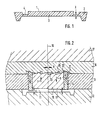
- Fig. 1 shows the sectional view a molding 1 made of plastic with different Wall thicknesses.
- the fitting 1 is rotationally symmetrical built up. It has an outer ring 2, which reinforces executed and profiled so that he at the later use in an annular housing groove can be attached.
- Inside the fitting 1 is a circular bottom or a membrane 3 with increased wall thickness provided.
- Fig. 2 shows a schematically shown Injection mold with which the molded part sketched in Fig. 1 1 can be manufactured.
- the injection mold shown includes in itself known manner, a first molded part or a mold plate 12 and a second molded part or a molded plate 13, with the help of not shown device elements moved along the center line 10 to open the mold can be.
- a molding space 11 or 11 ' In the illustrated closed Position define the molded parts 12, 13 between them a molding space 11 or 11 '.
- the molding space 11, 11 'in the embodiment shown is rotationally symmetrical is arranged to the center line 10 is the Invention on such a position of the mold space of course not limited. Others cannot either symmetrical arrangements are provided.
- Embodiment in molded part 13 is an arrangement consisting of an outer core member 14 and an inner stamp member 15 provided.
- the Elements 14, 15 can be relative to one another and to Molded part 13 are moved and have free end faces, that delimit the molding space 11 in some areas or define.
- the injection mold serves in the present embodiment the injection mold to make one disc-shaped molded part with an annular Cross-section thinning near its outer circumference.
- the outer core element 14 can consequently be cylindrical Have an axis configuration that coincides with the center line 10 of the mold space 11.
- the outer core member 14 is as indicated by the arrows 5, 6 indicated, between a first and second position relative to the opposite molded part 12 movable, each by suitable, not shown Appropriations are limited.
- the molding space 11 has a configuration in this position of the core element 14, which is essentially that of the one to be manufactured Fitting without reducing the wall thickness corresponds and is therefore also the starting mold space below 11 'designated.
- control element 16 in the direction arrow 9 can be by any suitable actuator (not shown), e.g. B. piston cylinder device, depending on the command one, too control device, not shown.
- suitable actuator e.g. B. piston cylinder device, depending on the command one, too control device, not shown.
- the arrangement of the interacting first Wedge surfaces 21, 22 is such that when the Control 16 in one direction (in the drawing to the right) the core element 14 the first or starting position takes while moving of the control element 16 in the opposite direction the core element 14 in the second, in the drawing left-hand, position is brought.
- a second pair of interacting wedge surfaces 23, 24 is on the inner stamp element 15 or Control element 16 is provided.
- the second wedge surfaces 23, 24 are in relation to the first wedge surfaces 21, 22 oppositely oriented so that the movement of the Control 16 movement in one direction of the stamp element 15 triggers in a direction that is opposite to that of the core element 14. at a displacement of the control element 16 in the Drawing to the left therefore experiences the stamp element 5 a movement in the direction of arrow 7 away from the opposite molded part 12, so that the Distance between the free end face of the stamp element 15 and the opposite wall area the mold space 11 slightly enlarged, while at the same time the distance between the free end face of the core element 14 the opposite wall area of the mold space 11 is reduced.
- the operation of the device described above is as follows. Not about that in the drawing The central sprue system shown becomes molten Plastic material injected into the starting mold space 11 ', whereby the core element 14 and stamp element 15 in the positions on the right in the drawing located so that the material without essential Disability due to the large gap "S" to the outer regions of the initial mold space 11 ' can flow and therefore its problem-free complete Filling is guaranteed. Immediately after completion the filling process is initiated by the control device Command to the actuating device of the control element 16 supplied, due to which the control 16 in one direction to the left in the drawing is moved along the arrow 9.
- the movement of the Control element 16 has the consequence that the core element 14 in the direction of arrow 5 in the second, in the drawing left-hand position is brought and the between its face and the opposite Wall of the mold space 11 displaced material becomes.
- the shift of the Control element 16 a movement of the inner stamp element 15 in a direction along arrow 7 away from the opposite molded part 12, whereby the distance between its free face and the opposite wall of the molding space 11 somewhat enlarged by that displaced by the core element 14 Volume.
- the Number of core and stamp elements 14, 15 shown and their arrangement among themselves and in relation to the mold space 11 are not limited, but any one Arrangement of one or more wall thickness reducing Core elements 14 with one or more stamp elements 15 can be provided.
- a stamp element 15 can be used to change the volume also be provided that through the core element 14 displaced material volume due to the still plastic Soul of the material in the mold space is led back into the sprue system.
- Others one Volume change-managing facilities, e.g. B. a membrane-like flexibility of a wall area of the mold space can also be provided his.
- the invention is on such a direction of movement is not restricted. Rather, the movements of the individual elements between their respective end positions adapted to the respective application and different be aligned.
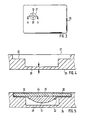
- FIG. 3 shows a chip card blank 26, which with the help of the procedure in particular can be produced advantageously.
- the blank card 26 has a recess 27 with the steps 28 and 33 in which a chip module at a later time is used.
- Fig. 4 the section A-B of Fig. 3 is schematic played. Because of the better overview dispenses with the exact reproduction of the proportions.
- the outer dimensions are usually such Chip cards about 85 mm x 54 mm, the thickness is 0.76 mm, the membrane 28 has at the bottom of the recess 27 a wall thickness of about 100 m.
- the outer The diameter of the recess 27 is approximately 15-20 mm, the shape of the recess can both in terms of outer outline as well as in the gradation arbitrarily vary. So z. B. rectangular, square or also known as oval outer outline.
- the deepening itself can also have several gradations or be lenticular in the inner region.
- Fig. 5 shows the section A-B of the map area with inserted chip module 44.
- the chip module exists thereby from a carrier film 29 on which metallic contact surfaces 30 are provided, via which at Use of the chip card 26 with the in the cast resin pill 31 arranged integrated circuit, or short Called chip (not shown) can.
- the chip module 44 has an adhesive layer 32 with the help of which the module is fixed in the Cutout 27 takes place.
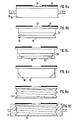
- Fig. 6 shows an injection mold for the production of Chip cards using the method according to the invention.
- the device consists essentially of a lower mold half 35 and an upper mold half 36. Between these two mold halves is the Molding space 38 provided the shape of the later Has a chip card, but without the one shown in FIG. 4 Indentation 27.
- the two mold halves 35 and 36 have an injection channel 39 through which the plastic material flows into the form.
- Stamp guide 46 provided over which the stamp 40 can be inserted into the mold space 38.
- the device shown in Fig. 6 has more Device elements, with the help of which in addition to the Production of the chip card blank described in the introduction also the simultaneous embedding of the chip module is possible.
- the upper mold half 36 is one more Guide plate 37 supplemented, which is also a stamp guide 46 has.
- the stamp 40 can thus through the guide plate 37 and the upper mold half 36 are pressed into the mold space.
- a transport channel 34 is provided, which Stamp guide 46 crosses and over the film tape 41 transported past the face of the stamp 40 can be.
- the film strip 41 is an "endless strip" executed and contains the chip modules lined up 44th
- stamp 40 no gradation, but a flat surface on.
- Suction air channels 43 are also provided, with the help of the film strip be sucked into the face of the stamp can.
- the film strip 41 is made in this way the end face of the stamp 40 arranged that a Chip card module 44 is positioned in front of it.
- the punch 40 By Lowering the punch 40 in the direction of the molding space 38 (Arrow 42) the chip module in the stamp guide of the Molded part 36 pressed and punched out of the film strip 41.
- the die-cut chip module is over the Suction channels 43 sucked in and thus on the end face of the stamp held.
- the stamp 40 is now ready lowered in the direction of the molding space 38, that the lower edge of the chip module approximately with the upper edge of the Forms 38 completes, d. H. the chip module still does not protrude into the mold space.
- the plastic material is injected via the injection channel 39. After sufficient filling of the mold space is the stamp together with the chip module in the Plastic compound pressed in so far that the flat end face of the stamp 40 flush with the later Card surface completes.
- the mold is opened, i.e. H. the mold halves 35 and 36 moved apart and by renewed Activate the stamp 40 ejected from the mold.
- the separation of the card from that in the injection channel 39 located plastic mass takes place in a known manner either by tearing it off or cutting it off with the help of cutting elements, not shown.
- the stamp 40 After closing the two mold halves 35 and 36, the stamp 40 is retracted into the starting position and the one with the punched-out 45 Area of the film tape moved on until again Chip module 44 is positioned in front of the stamp 40.
- the card manufacturing process shown in Fig. 6 thus enables the production of injection molded chip cards with simultaneous embedding of the chip module. Pressing the chip module into the injected one Tests have shown that plastic mass is relative unproblematic, as long as the outer shape of the chip module simply structured and the module mechanical is resilient. For complex structured modules or also when using large chip components (such as microprocessor chips) it may be advisable before embedding the module in the cavity Create card. This is done in a simple manner in that the process sequence described for FIG. 6 modified and a stamp 40 is used with to accomplish these additional functions are.
- stamp 40 shows a possible embodiment of a such equipped with additional functions Stamp 40.
- the stamp 40 consists of three one inside the other sliding stamp elements 47, 48 and 49.
- the Stamp 40 becomes in the form shown in Fig. 7a Pressing the recess 27 used. For this the Stamp through the foil punching 45 of the foil strip 41 brought through to the mold space 38, the plastic material is injected into the mold space and, as described initially, in the molding compound pressed.
- the stamp is 40 in the guide plate 37 withdrawn. Besides, will the stamp element 48 moves back until the end face of element 48 with the end face of the element 49 ends flush. Furthermore, the pin 47 in the position shown in Fig. 7b withdrawn and fixed. In this position there is a in the center of the Air channel opening into the face of the stamp, through a Bore in element 48 and one provided in element 49 Longitudinal groove 50 suctioning the chip module 44 allowed.
- the stamp 40 After the stamp 40 by withdrawing the Elements 47 and 48 in the arrangement shown in Fig. 7b brought and the film strip 41 by a position has been moved, the stamp 40 is again in the direction Formraum printed, being, as at the beginning a chip module 44 from the film strip 41 punched out and this in the previously created graded Placement placed. That with an adhesive layer 32 equipped chip module 44 is now with the stamp 40 pressed into the recess 27. The residual heat of the plastic material activates the hot glue and fixes it the module in the card body.
- the mold halves can 35 and 36 are opened again and the Card body can be removed from the form.
- chip modules with anchoring elements that Module in addition or as an alternative to an adhesive layer in anchor the card body are chip modules with anchoring elements that Module in addition or as an alternative to an adhesive layer in anchor the card body.
- Such a module is already from DE 31 31 216 C2 known and shown in Fig. 8a.
- the chip module exists a carrier film 29 on which contact surfaces 30 lie, which are conductively connected to the chip.
- To the Protection against mechanical loads are chip module and conductive connections from a cast body 55 surround.
- Anchoring elements protrude over the edge of the cast body 55 56, which is exclusively the Anchor the module in the card body.
- the anchoring element 56 as perforated ring to be formed in the map material is to be embedded.
- the holes are penetrated by the map material, so that the chip module is anchored in the card is guaranteed.
- Fig. 8c is a chip module with both recesses in the lateral surface as well as in the end face of the Cast body shown.
- the recess 59 in the lateral surface is ring-shaped and prevents Remove the chip module from the card body.
- the angled recesses 60 anchor the module additionally in the card body, but prevent beyond also twisting the module in the card.
- FIG. 8d shows a chip module, the cast body 55 thereof is penetrated by channels 58.
- the channels open on the one hand in the bottom surface of the module and on the other hand in the outer surface of the cast body.
- the channels point for example, an inclination of approximately 45 °.
- the in Fig. 8d chip module is particularly suitable if the module into the already injected plastic compound to be pressed in, since the channels 58 are also present very good from the still liquid plastic material be flowed through.
- the openings are to prevent use of the card arranged in the lateral surface so that they at pressed chip module positioned approximately in the middle of the card are. The ones that appear here with the card bent Forces are minimal, causing damage to the anchor by bending the card is not expected.
- FIG. 8e shows a chip module with a cast body 55, the outer surface of which is designed as a thread.
- the comparatively complex thread structure forms by pressing the module into the not yet solidified plastic mass as an exact negative form.
- the cast body and the card body educational materials chosen so that they are not connect with each other this can be done with the thread module anchored to the card body later from this be unscrewed.
- the invention Process of making a smart card with exchangeable module, without additional process steps to have to provide.
- FIG. 8f shows the module shown in FIG. 8e 55 in connection with a threaded sleeve 61.
- the sleeve has anchoring elements 56, via which the sleeve can be fixed in the card body.
- the sleeve 61 is either with or without screwed-in module 55 during the injection process into the card body brought in. To prevent the sleeve from deforming, is the insertion together with the chip module or a corresponding module dummy preferable.
- the sleeve 61 shown in Fig. 8f is with an anchoring frame equipped, as shown in Fig. 8a is. This protrudes beyond the edge of the sleeve 61 and ensures particularly good anchoring of the unit Chip module / sleeve in the card body.
- other anchoring elements are also wise usable such. B. those shown in Figs. 8b - 8e. Instead of the thread in this embodiment another detachable connection, such as. Legs Type bayonet lock, can be selected.
- Standard card 65 with an integrated mini chip card 66 as for example from DE 40 07 221 A1 is known.
- mini chip cards 66 are usually made of conventional standard cards 65 punched out.
- Standard card 65 with integrated mini chip card 66 can also with the help of the invention Injection molding process without subsequent punching processes getting produced. This is, for example, that in FIG. 6 Modify the injection mold shown.
- Fig. 10 shows such an adapted injection mold.
- the Stamping tool 69 has the shape of the in Fig. 9 in the Standard card 65 shown punching gap 75.
- stamping tool 69 closes the effective face of the Stamping tool 69 with the surface of the molding space the lower mold half 35 flush.
- the Stamping tool 69 is in the lower mold half 35 fitted so that it is with the help of the gripper 74 can be inserted into the mold space that but there is no gap over which it enters the mold space injected plastic compound can escape.
- the End face of the punch 69 are at the points where the connecting webs 67 should be generated, "notches" provided in Shape and size of the later connecting bars correspond.
- the production of the norm cards with integrated Mini chip cards are made in the usual way, i. H. like in 6 and 7 explained.
- the punch 69 pressed into the mold space with the aid of the grippers 74 to produce the outline 75 and the webs 67.
- the punching tool solidifies the card material removed with the grippers 74 from the mold space 38 and after opening the injection mold the card taken.
Abstract
Description
Die Erfindung betrifft ein Verfahren und eine Vorrichtung zum Herstellen von Chipkarten und Chipkarten-Rohlingen mit bereichsweise reduzierter Wandstärke durch Einspritzen eines schmelzflüssigen Kunststoffmaterials in einen Formraum und anschließendem Abkühlen des Kunststoffmaterials.The invention relates to a method and a device for the production of chip cards and chip card blanks with reduced wall thickness in some areas by injecting a molten plastic material into a mold room and then cooling of the plastic material.
Chipkarten mit einem Kartenkörper aus Kunststoffmaterial sind seit langem bekannt. So ist beispielsweise aus der FR-A 2 579 799 eine Chipkarte mit einem Kartenkörper aus PVC bekannt, der eine mehrstufige Vertiefung für das Chipmodul enthält. Das Modul wird unter Wärmeeinwirkung in die mit Noppen versehene Aussparung eingepreßt. Während des Einpressens dienen die Noppen, die bei diesem Vorgang erweichen und auf ein vorbestimmtes Maß zusammengedrückt werden, als Abstandselemente, so daß nachträglich ein Flüssigkleber mit definierter Klebeschicht zwischen dem Modul und der Karte aufgebracht werden kann. Bei entsprechender Dosierung kann auf diese Weise ein Austreten des Klebers auf die Kartenoberfläche vermieden werden. Es ist der FR-A 2 579 799 nicht im einzelnen zu entnehmen, wie der Kartenkörper selbst hergestellt wird.Chip cards with a card body made of plastic material have been known for a long time. For example from FR-A 2 579 799 a chip card with a Card body made of PVC known to be a multi-stage Contains recess for the chip module. The module will under the influence of heat in the studded Recess pressed in. During the pressing serve the knobs that soften in this process and compressed to a predetermined level are, as spacers, so that a later Liquid adhesive with a defined adhesive layer between the Module and the card can be applied. at appropriate dosage can be in this way Avoid leakage of the adhesive on the card surface become. FR-A 2 579 799 is not in the individual as the card body itself will be produced.
Aus der EP 0 277 854 A1 und aus der EP 0 267 826 A1 sind indes spritzgußtechnische Herstellungsverfahren für Chipkarten bzw. Chipkartenrohlinge, die einen Membranbereich bzw. eine Vertiefung zur Aufnahme des Chipmoduls aufweisen, bekannt.From EP 0 277 854 A1 and from EP 0 267 826 A1, however, are injection molding manufacturing processes for chip cards or chip card blanks that one Membrane area or a recess for receiving of the chip module known.
Bei dem in der EP 0 277 854 A1 vorgestellten Verfahren zur Herstellung der Karte befindet sich das Modul während des Einspritzvorganges bereits in der Gußform und wird dort durch Saugluft gehalten. Durch eine im Hohlraum der Gußform befindliche federnd gelagerte Platte, die das Modul gegen die obere Gußform preßt, wird eine zusätzliche Positionierung und Fixierung des Moduls vor dem Spritzgießen sichergestellt. Der Kunststoff wird über eine Seitenkante der Form eingespritzt, wobei sich die Platte aufgrund des hierbei entstehenden Drucks auf Kartendicke absenkt.In the method presented in EP 0 277 854 A1 the module for making the card is located already in the mold during the injection process and is held there by suction air. Through an im Cavity of the mold located resiliently mounted Plate that presses the module against the upper mold, is an additional positioning and fixation of the Module before injection molding. Plastic is injected over one side edge of the mold, where the plate due to the resulting Reduced pressure on card thickness.
Das Verfahren ermöglicht es, eine Chipkarte in einem Arbeitsgang herzustellen. Da sich das Modul während des Einspritzvorgangs im Formraum befindet, wirkt es jedoch wie ein in die Gußform ragender Stempel. Aufgrund der seitlichen Einspritzung des Materials teilt sich der Kunststoffstrom vor dem Modul bzw. vor einem Stempel in zwei Ströme auf, diedas Hindernis umfließen und sich hinter diesem wieder vereinigen. Dabei entstehen hinter dem im Formraum befindlichen Hindernis bevorzugte Molekularorientierung in Fließrichtung, die sich im Extremfall als Sollbruchstellen auswirken. Darüber hinaus erlaubt die durch den seitlichen Einspritzkanal festgelegte Strömungsrichtung nicht die Ausbildung komplexer, scharfer Konturen im Bereich der Membran, wie sie beispielsweise zur Bildung von Verankerungselementen für das Modul notwendig sind. Schließlich kann es bei seitlicher Einspritzung im Membranbereich durch Lufteinschlüsse zu Blasenbildung kommen.The process enables a smart card to be inserted manufacture in one operation. Because the module is in the mold space during the injection process, however, it looks like a stamp protruding into the mold. Due to the side injection of the material divides the plastic flow in front of the module or in front of one Stamps in two streams that flow around the obstacle and reunite behind it. This creates behind the obstacle in the molding space preferred molecular orientation in the flow direction, the in extreme cases act as predetermined breaking points. It also allows through the side injection channel fixed flow direction not training complex, sharp contours in the area of Membrane, such as those used to form anchoring elements are necessary for the module. Finally, with side injection in the membrane area due to air pockets to form bubbles come.
In der EP 0 267 826 A1 wird ein Verfahren zur Herstellung von Chipkarten-Rohlingen in Spritzgußtechnik vorgestellt. Die verwendete Gußform ist aus planparallelen Platten gebildet, die gegeneinander beweglich sind. In einer der Platten ist der Einspritzkanal vorgesehen. Gegenüber diesem ist in der anderen Platte ein in die Gußform ragender und mit Kühlkanälen versehener Stempel angeordnet, durch den die Aussparung zur späteren Aufnahme für das Chipmodul in der Karte geformt wird. Der Stempel hat auf seiner Stirnfläche Vertiefungen zur Erzeugung von Noppen im Boden der Modulaussparung. Wird das Chipmodul in die Aussparung eingebracht, liegt es auf den Noppen auf, so daß der Spalt zwischen dem Chipmodul und dem Boden mit einem Kleber zur Befestigung des Moduls aufgefüllt werden kann.EP 0 267 826 A1 describes a process for the production of chip card blanks in injection molding technology presented. The mold used is plane-parallel Plates formed that are movable against each other are. The injection channel is provided in one of the plates. Opposite this is an in in the other plate the mold protruding and provided with cooling channels Stamp arranged through which the recess for later Shaped receptacle for the chip module in the card becomes. The stamp has depressions on its face for creating knobs in the bottom of the module recess. The chip module is in the recess introduced, it lies on the knobs, so that the Gap between the chip module and the floor an adhesive for attaching the module can.
Das in der EP 0 267 826 A1 vorgestellte Verfahren behebt aufgrund der Lage des Einspritzkanals die Nachteile des in der EP 0 277 254 A1 genannten Verfahrens. Insbesondere entstehen keine Vorzugsbruchstellen und können im Bereich der Stirnfläche des Stempels komplexe, scharfe Konturen (Noppen) ausgebildet werden. Wegen der Lage des Einspritzkanals liegt der zwangsläufig entstehende Einspritznippel jedoch im Bereich der Membran auf der Rückseite des Karten-Rohlings, was das optische Erscheinungsbild der fertiggestellten Karte beeinträchtigt. Gravierender ist aber, daß das Kunststoffmaterial zunächst in den Bereich mit reduzierter Wandstärke eingespritzt wird, um dann unter beträchtlichem Druckverlust in die übrigen Bereiche zu fließen. Aufgrund dessen besteht die Gefahr der unvollständigen Füllung der peripheren Bereiche des Formraums mit Kunststoffmaterial.The method presented in EP 0 267 826 A1 eliminates the disadvantages due to the location of the injection channel of the method mentioned in EP 0 277 254 A1. In particular, there are no preferred breakpoints and complex, sharp contours (nubs) are formed. Because of the location of the injection channel inevitably arising injection nipples in the Area of the membrane on the back of the card blank, what the visual appearance of the finished Card affected. But more serious is that the plastic material first in the area with reduced wall thickness is injected, then under considerable pressure loss in the remaining areas flow. Because of this, there is a risk of incomplete Filling the peripheral areas of the molding space with plastic material.
Zusammenfassend läßt sich sagen, daß beide Verfahren eine kostengünstige Herstellung von Chipkarten bzw. Chipkarten-Rohlingen erlauben, die jedoch mit Qualitätseinbußen verbunden sind.In summary, both procedures an inexpensive production of chip cards or allow chip card blanks, but with Losses in quality are associated.
Der Erfindung liegt demgegenüber die Aufgabe zugrunde, ein Verfahren und eine Vorrichtung der eingangs erwähnten Gattung zu schaffen, die eine wirtschaftliche Fertigung von Chipkarten und Chipkarten-Rohlingen mit in Teilbereichen erheblich reduzierter Wandstärke ohne die geschilderten Einschränkungen ermöglichen.In contrast, the object of the invention based on a method and a device of the introduction mentioned genus to create an economic Production of chip cards and chip card blanks with significantly reduced in some areas Wall thickness without the restrictions described enable.
Erfindungsgemäß wird diese Aufgabe durch die Merkmale der nebengeordneten Ansprüche gelöst.According to the invention, this object is achieved by Features of the independent claims solved.
Aus der DE-A 34 01 644 ist zwar ganz allgemein das Herstellen von Spritzgußteilen, bei denen Aussparungen durch das Einfahren eines beweglichen Stempels erzielt werden, bekannt. Die DE-A 34 01 644 geht an keiner Stelle auf die spezifischen Verfahrensschritte ein, die zur Herstellung einer Chipkarte notwendig sind. From DE-A 34 01 644 this is very general Manufacture of injection molded parts with recesses by retracting a movable stamp be achieved. DE-A 34 01 644 addresses no place on the specific procedural steps, which are necessary for the production of a chip card.
Gemäß der Erfindung werden die beweglichen Elemente der Spritzgußform nicht nur zur Herstellung der dünnen Wandbereiche, sondern auch zur Einbettung des Chipmoduls in die Kunststoffmasse des Kartenkörpers benützt. Wie anhand der Ausführungsbeispiele noch weiter erläutert wird, kann dies auf verschiedene Weise geschehen. Um die Vielfalt der Möglichkeiten zu veranschaulichen, werden hierzu zwei Ausführungsvarianten beschrieben.According to the invention not only the moving elements of the injection mold to manufacture the thin wall areas, but also for embedding the chip module in the plastic mass of the card body used. As with the examples explained further, this can happen in different ways. To the diversity of There are two ways to illustrate this Design variants described.
Bei einer dieser Ausführungsformen wird mit einem beweglichen Stempel ein an der Stirnseite des Stempels fixiertes Mikrochipmodul, wie es für Chipkarten üblicherweise Anwendung findet, in die Kunststoffmasse gepreßt. Auf diese Weise wird in einem einzigen Arbeitsgang sowohl das Modul in den Kartenkörper eingebracht und fixiert als auch der dafür benötigte Hohlraum geschaffen.In one of these embodiments, a movable stamp on the front of the stamp fixed microchip module, as is usually the case for chip cards Applies to the plastic mass pressed. This way, in a single operation both the module inserted into the card body and fixed as well as the required cavity created.
Bei der zweiten Ausführungsform wird das Einbetten des Moduls in zwei Schritte unterteilt, wobei in einem ersten Schritt durch Einpressen des Stempels der Hohlraum geschaffen wird, in einem zweiten, direkt anschließenden Schritt wird das Modul in diesen Hohlraum eingesetzt. Die Fixierung im Hohlraum erfolgt mit Hilfe einer am Modul vorgesehenen Heißkleberbeschichtung, die von der Restwärme des Spritzgußkartenkörpers aktiviert wird.In the second embodiment, embedding of the module divided into two steps, one first step by pressing the die into the cavity is created in a second, directly Subsequent step is the module in this cavity used. The fixation in the cavity takes place with With the help of a hot glue coating provided on the module, from the residual heat of the Injection molded card body is activated.
Das erfindungsgemäße Verfahren weist gegenüber den bekannten Möglichkeiten eine Vielzahl von Vorteilen auf. So kann beispielsweise die Stirnfläche der beweglichen Stempel nahezu beliebig kompliziert strukturiert sein. Durch Einpressen des Stempels in die Kunststoffmasse erhält man stets einen exakten Abdruck dieser Strukturen. Die Bildung von Blasen, Fehlstellen, unscharfer Konturen etc. wird vollständig vermieden.The method according to the invention points to the known possibilities have a number of advantages on. For example, the end face of the movable Stamp structure almost any complexity his. By pressing the stamp into the plastic mass you always get an exact impression of it Structures. The formation of bubbles, defects, blurred contours etc. are completely avoided.
Da der Stempel erst nach dem Einfließen der Kunststoffmasse in diese eingepreßt wird, ist die Molekülorientierung über das ganze Volumen der Karte einheitlich, d. h. auf unterschiedliche Molekülorientierung zurückzuführende Vorzugsbruchlinien entstehen nicht. Üblicherweise ist mit derartigen Vorzugsbruchlinien zu rechnen, wenn die Kunststoffmasse während des Einspritzens in die Form eingesetzte Formelemente umströmt bzw. an den Stellen, an denen die verschiedenen Kunststoffströme nach Umfließen des "Hindernisses" aufeinandertreffen.Since the stamp only after the plastic mass has flowed in the molecular orientation is pressed into it across the entire volume of the card uniform, d. H. to different molecular orientations preferential break lines to be returned Not. Usually with such preferred break lines to be expected if the plastic mass during the Injection molded elements used in the mold flows around or at the points where the different Plastic flows after flowing around the "Obstacle" meet.
Da die dünnen Wandbereiche durch Pressen der bereits eingeströmten Kunststoffmasse erzeugt wird, erhält man nicht nur die exakte Form- und Wandstärke auch sehr dünner Membranen, in diesen Bereichen wird auch durch Komprimieren der Kunststoffmasse eine erhöhte Festigkeit des derart verdichteten Kunststoffmaterials erreicht. Gerade dies ist bei Chipkarten von besonderem Interesse, da die Karten in den anschließenden Druckvorgängen (Aufbringen des Druckbildes) sowie im späteren Kartengebrauch besonderen Belastungen ausgesetzt sind.Since the thin wall areas by pressing the plastic mass which has already flowed in is produced, you get not only the exact shape and wall thickness also very thin membranes, in these areas also by compressing the plastic mass increased strength of the plastic material thus compacted reached. This is precisely the case with chip cards from of special interest since the cards in the subsequent printing processes (application of the Printed image) as well as later in card use Are exposed to loads.
Weitere Vorteile und Ausführungsvarianten sind den nachfolgenden Beispielen zu entnehmen, die anhand der Figur beschrieben sind.Further advantages and design variants are the The following examples can be seen from the the figure are described.
Es zeigen:
- Fig. 1
- die Schnittzeichnung einer rotationssymmetrischen Membrane mit unterschiedlichen Wandstärkenbereichen,
- Fig. 2
- eine Spritzgußform in fragmentarischer geschnittener Ansicht in Stellungen zum Zeitpunkt des Formfüllvorganges und der Wandstärkenreduzierung,
- Fig. 3
- einen Chipkartenrohling in Aufsicht,
- Fig. 4
- den Schnitt A-B aus Fig. 3,
- Fig. 5
- den Schnitt A-B mit eingesetztem Chipmodul,
- Fig. 6
- eine Vorrichtung zum Herstellen von Spritzgußkarten in vereinfachter Schnittdarstellung,
- Fig. 7
- alternative Vorrichtungselemente zum Herstellen von Spritzgußkarten,
- Fig. 8a - e
- alternative Chipmodule zum vorteilhaften Einbau in Spritzgußkarten,
- Fig. 9
- eine Normkarte mit integrierter Minichipkarte in Aufsicht,
- Fig. 10
- eine Vorrichtung zum Herstellen von Normkarten mit integrierter Minichipkarte in vereinfachter Schnittdarstellung.
- Fig. 1
- the sectional drawing of a rotationally symmetrical membrane with different wall thickness ranges,
- Fig. 2
- an injection mold in a fragmentary sectional view in positions at the time of the mold filling process and the reduction in wall thickness,
- Fig. 3
- a chip card blank under supervision,
- Fig. 4
- the section AB from Fig. 3,
- Fig. 5
- the section AB with the chip module inserted,
- Fig. 6
- a device for producing injection-molded cards in a simplified sectional view,
- Fig. 7
- alternative device elements for the production of injection molded cards,
- 8a-e
- alternative chip modules for advantageous installation in injection molding cards,
- Fig. 9
- a standard card with integrated mini chip card under supervision,
- Fig. 10
- a device for producing standard cards with an integrated mini chip card in a simplified sectional view.
Fig. 1 zeigt die Schnittdarstellung
eines Formstücks 1 aus Kunststoff mit unterschiedlichen
Wandstärken. Das Formstück 1 ist rotationssymmetrisch
aufgebaut. Es weist einen äußeren Ring 2 auf, der verstärkt
ausgeführt und derart profiliert ist, daß er bei der
späteren Anwendung in einer ringförmigen Gehäusenut
befestigt werden kann. Im Inneren des Formstücks 1 ist
ein kreisförmigen Boden bzw. eine Membran 3 mit
erhöhter Wandstärke vorgesehen. Zwischen dem
äußeren Ring 2 und der Membran 3 ist eine ringförmige
Wandstärkenreduzierung 4 vorgesehen, die eine elastische
Einbettung der Membrane 3 bewirkt.Fig. 1 shows the sectional view
a
Fig. 2 zeigt eine schematisch dargestellte Spritzgußform, mit der das in Fig. 1 skizzierte Formteil 1 hergestellt werden kann.Fig. 2 shows a schematically shown Injection mold with which the molded part sketched in Fig. 1 1 can be manufactured.
Die dargestellte Spritzgießform umfaßt in an sich
bekannter Weise ein erstes Formteil bzw. eine Formplatte
12 und ein zweites Formteil bzw. eine Formplatte
13, die mit Hilfe nicht dargestellter Vorrichtungselemente
zum Öffnen der Form längs der Mittellinie 10 verschoben
werden können. In der dargestellten geschlossenen
Position definieren die Formteile 12, 13 zwischen sich
einen Formraum 11 bzw. 11'. Obschon der Formraum
11, 11' bei der dargestellten Ausführungsform rotationssymmetrisch
zur Mittellinie 10 angeordnet ist, ist die
Erfindung auf eine derartige Lage des Formraumes
natürlich nicht beschränkt. Es können auch andere nicht
symmetrische Anordnungen vorgesehen werden.The injection mold shown includes in itself
known manner, a first molded part or a
In einem der Formteile 12, 13, bei der vorliegenden
Ausführungsform im Formteil 13, ist eine Anordnung,
bestehend aus einem äußeren Kernelement 14 und
einem inneren Stempelelement 15, vorgesehen. Die
Elemente 14, 15 können relativ zueinander und zum
Formteil 13 bewegt werden und besitzen freie Stirnflächen,
die den Formraum 11 bereichsweise begrenzen
bzw. definieren.In one of the molded
Wie bereits erwähnt, dient bei der vorliegenden Ausführungsform
die Spritzgießform zum Herstellen eines
scheibenförmigen Formteiles mit einer ringförmigen
Querschnittverdünnung nahe seinem äußeren Umfang.
Das äußere Kernelement 14 kann demzufolge eine zylinderförmige
Konfiguration mit einer Achse haben, die
mit der Mittellinie 10 des Formraumes 11 zusammenfällt.As already mentioned, serves in the present embodiment
the injection mold to make one
disc-shaped molded part with an annular
Cross-section thinning near its outer circumference.
The
Das äußere Kernelement 14 ist, wie durch die Pfeile
5, 6 angedeutet, zwischen einer ersten und zweiten Stellung
relativ zum gegenüberliegenden Formteil 12
bewegbar, die jeweils durch nicht gezeigte geeignete
Mittel anschlagbegrenzt sind. Bei der Ausgangsstellung
(in der Zeichnung rechts) ist der Abstand "S" zwischen
der freien Stirnfläche des Kernelements 14 und einem
gegenüberliegenden Wandbereich des Formraumes 11
relativ groß, da das Kernelement 14 im Formteil 13 im
wesentlichen versenkt ist. Im Bereich des Kernelementes
14 liegt somit keine Querschnittsverengung vor,
die das Material am Einfließen von einer nicht gezeigten
zentralen Angießstelle zu den äußeren Begrenzungen
des Formraumes 11 hindern könnten. Der Formraum 11
hat in dieser Stellung des Kernelementes 14 eine Konfiguration,
die im wesentlichen derjenigen des zu fertigenden
Formstückes ohne Wandstärkenreduktion
entspricht und wird deshalb nachfolgend auch Ausgangsformraum
11' bezeichnet.The
In der zweiten, in der Zeichnung auf der linken Seite
gezeigten, Stellung wurde das Kernelement 14 in den
Formraum 11 verschoben, wodurch der Abstand
zwischen seiner freien Stirnfläche und dem gegenüberliegenden
Wandbereich des Formraumes 11 auf ein
Maß "s" herabgesetzt. Dieses Maß "s" entspricht der
gewünschten reduzierten Wandstärke am zu fertigenden
Formstück.In the second, in the drawing on the left
shown, the
Obschon andere geeignete Einrichtungen vorgesehen
werden können, dient bei der vorliegenden Ausführungsform
zur Steuerung der Bewegung des
Kernelements 14 zwischen der ersten und zweiten Stellung
eine Anordnung aus zusammenwirkenden ersten
Keilflächen 21, 22 an der dem Formraum 11 abgewandten
Stirnseite des Kernelementes 14 bzw. an einem
zwischen dem Formteil 13 und einer Stützplatte 17 verschiebbar
angeordneten Steuerelement 16. Die Keilflächen
21, 22 bewirken, daß die translatorische hin-und
hergehende Bewegung des Steuerelementes 16 (vgl.
Pfeil 9) in eine Bewegung des Kernelementes 14 in Richtung
der Pfeile 5 bzw. 6 umgesetzt wird. Es versteht sich,
daß zu diesem Zweck auch andere geeignete Einrichtungen,
z. B. eine Solenoid- oder hydraulische Kolben/Zylindereinrichtung,
vorgesehen werden können.Although other suitable facilities are provided
serves in the present embodiment
to control the movement of the
Die Bewegung des Steuerelementes 16 in Richtung
des Pfeiles 9 kann durch irgendeine geeignete Betätigungseinrichtung
(nicht gezeigt), z. B. Kolbenzylindereinrichtung,
in Abhängigkeit des Befehls einer, ebenfalls
nicht gezeigten, Steuereinrichtung erfolgen.The movement of the
Die Anordnung der zusammenwirkenden ersten
Keilflächen 21, 22 ist so, daß bei einer Bewegung des
Steuerelementes 16 in eine Richtung (in der Zeichnung
nach rechts) das Kernelement 14 die erste oder Ausgangsposition
einnimmt, während bei einer Bewegung
des Steuerelementes 16 in die entgegengesetzte Richtung
das Kernelement 14 in die zweite, in der Zeichnung
linksseitige, Position gebracht wird.The arrangement of the interacting first
Wedge surfaces 21, 22 is such that when the
Ein zweites Paar zusammenwirkende Keilflächen
23, 24 ist am inneren Stempelelement 15 bzw.
Steuerelement 16 vorgesehen. Die zweiten Keilflächen
23, 24 sind in Bezug auf die ersten Keilflächen 21, 22
entgegengesetzt orientiert, so daß die Bewegung des
Steuerelementes 16 in eine Richtung eine Bewegung
des Stempelelementes 15 in eine Richtung auslöst, die
entgegengesetzt zu der des Kernelementes 14 ist. Bei
einer Verschiebung des Steuerelementes 16, in der
Zeichnung nach links, erfährt daher das Stempelelement
5 eine Bewegung in Richtung des Pfeiles 7 weg
vom gegenüberliegenden Formteil 12, so daß sich der
Abstand zwischen der freien Stirnfläche des Stempelelementes
15 und dem gegenüberliegenden Wandbereich
des Formraumes 11 etwas vergrößert, während
gleichzeitig der Abstand zwischen der freien Stirnfläche
des Kernelementes 14 dem gegenüberliegenden Wandbereich
des Formraumes 11 verringert wird.A second pair of interacting wedge surfaces
23, 24 is on the
Durch geeignete Abstimmung der Neigung der
ersten und zweiten Keilflächen 21, 22 bzw. 23, 24 kann
erreicht werden, daß die durch die Bewegung des Stempelelementes
15 erzielte Vergrößerung des Volumens
des Formraumes 11 im wesentlichen der Abnahme des
Volumens infolge der Bewegung des Kernelementes 14
in die zweite Stellung entspricht. Auf diese Weise kann
erreicht werden, daß das Gesamtvolumen des Formraumes
11 sowohl in der ersten als auch zweiten Stellung
des Kernelementes 14 im wesentlichen verändert
ist. Es versteht sich jedoch, daß die Erfindung nicht auf
einen im wesentlichen vollständigen Volumenausgleich
beschränkt ist. Vielmehr können, wenn erwünscht, die
von den Elementen 14, 15 verdrängten bzw.
geschaffenen Teilvolumina voneinander abweichen,
wodurch sich besondere Wirkungen am zu fertigenden
Formstück, z. B. eine Materialverdichtung, erzielen lassen.By appropriately matching the inclination of the
first and second wedge surfaces 21, 22 and 23, 24, respectively
achieved that by the movement of the
Die Funktionsweise der vorbeschriebenen Vorrichtung
ist wie folgt. Über das in der Zeichnung nicht
gezeigte zentrale Angießsystem wird schmeizflüssiges
Kunststoffmaterial in den Ausgangsformraum 11' eingespritzt,
wobei sich das Kernelement 14 und Stempelelement
15 in den in der Zeichnung rechten Positionen
befinden, so daß das Material ohne wesentliche
Behinderung durch den großen Spalt "S" zu den
äußeren Bereichen des Ausgangsformraumes 11'
fließen kann und damit dessen problemlose vollständige
Füllung gewährleistet ist. Unmittelbar nach Beendigung
des Füllvorganges wird von der Steuereinrichtung ein
Befehl an die Betätigungseinrichtung des Steuerelementes
16 geliefert, aufgrund dessen das Steuerelement
16 in eine Richtung in der Zeichnung nach links
längs des Pfeiles 9 bewegt wird. Die Bewegung des
Steuerelementes 16 hat zur Folge, daß das Kernelement
14 in Richtung des Pfeiles 5 in die zweite, in der Zeichnung
linksseitige, Position gebracht wird und dabei das
zwischen seiner Stirnfläche und der gegenüberliegenden
Wand des Formraumes 11 befindliche Material verdrängt
wird. Gleichzeitig bewirkt die Verschiebung des
Steuerelementes 16 eine Bewegung des inneren Stempelelementes
15 in eine Richtung längs des Pfeiles 7
weg vom gegenüberliegenden Formteil 12, wodurch sich
der Abstand zwischen seiner freien Stirnfläche und der
gegenüberliegenden Wand des Formraumes 11 etwas
vergrößert, um das durch das Kernelement 14 verdrängte
Volumen aufzunehmen.The operation of the device described above
is as follows. Not about that in the drawing
The central sprue system shown becomes molten
Plastic material injected into the starting mold space 11 ',
whereby the
Die auf der linken Seite der Zeichnung gezeigte Stellung
der Teile wird solange beibehalten, bis das Material
im Formraum 11 abgekühlt und das erhaltene Formstück
nach Öffnen der Form durch geeignete mechanische
oder pneumatische Einrichtungen aus dem Formraum
ausgeworfen worden ist. Im Wirkbereich des äußeren
Kernelementes 14 verbleibt danach im Formstück eine
dem Spalt "s" entsprechende Wandstärke, die, wenn
erwünscht, um ein Vielfaches kleiner als die Wandstärke
an benachbarten Bereichen des Formstückes sein kann.
Versuche haben gezeigt, daß das erfindungsgemäße
Verfahren ohne weiteres eine Reduzierung von einer
Ausgangswandstärke von z. B. 0,8 mm auf 0,15 mm oder
weniger ermöglicht, ohne daß Bindenähte oder Lufteinschlüsse
an den gefertigten Formstücken auftraten. Da
der Formfüllvorgang durch keine Querschnittsverengung
des Formraumes eingeschränkt ist, lassen sich mit
dem Verfahren praktisch sämtliche
thermoplastische Kunststoffmaterialien verarbeiten. Die
diesbezüglichen, bei herkömmlichen Verfahren zum
Spritzen dünner Wandstärken bestehenden Einschränkungen
entfallen.The position shown on the left side of the drawing
the parts are kept until the material
cooled in the
Es versteht sich, daß die
gezeigte Anzahl der Kern- und Stempelelemente 14, 15
und deren Anordnung untereinander und in Bezug auf
den Formraum 11 nicht beschränkt sind, sondern eine beliebige
Anordnung eines oder mehrerer wandstärkenreduzierender
Kernelemente 14 mit ein oder mehreren Stempelelementen
15 vorgesehen werden kann. Anstelle
eines Stempelelementes 15 kann zur Volumenänderung
auch vorgesehen sein, daß das durch das Kernelement
14 verdrängte Materialvolumen durch die noch plastische
Seele des im Formraum anstehenden Materials
zurück in das Angießsystem geführt wird. Andere, eine
Volumenänderung bewerkstelligende, Einrichtungen, z.
B. eine membranartige Nachgiebigkeit eines Wandbereiches
des Formraumes, können ebenfalls vorgesehen
sein.It is understood that the
Number of core and stamp
Bei der gezeigten Ausführungsform erfolgt die
Bewegung der Elemente 14, 15 im wesentlichen parallel
zueinander zu der Mittellinie 10. Die Erfindung ist auf
eine derartige Bewegungsrichtung nicht beschränkt.
Vielmehr können die Bewegungen der einzelnen Elemente
zwischen ihren jeweiligen Endstellungen dem
jeweiligen Anwendungsfalls angepaßt und unterschiedlich
ausgerichtet sein.In the embodiment shown, the
Movement of the
Fig.3 zeigt einen Chipkartenrohling 26, der mit Hilfe
des Verfahrens in besonders
vorteilhafter Weise hergestellt werden kann. Der Kartenrohling
26 weist eine Vertiefung 27 mit den Stufen 28 und
33 auf, in die zu einem späteren Zeitpunkt ein Chipmodul
eingesetzt wird.3 shows a
In Fig. 4 ist der Schnitt A-B der Fig. 3 schematisch
wiedergegeben. Der besseren Übersicht wegen wurde
auf die exakte Wiedergabe der Proportionen verzichtet.
Üblicherweise sind die äußeren Abmaße derartiger
Chipkarten etwa 85 mm x 54 mm, die Dicke beträgt 0,76
mm, die Membran 28 am Boden der Vertiefung 27 weist
eine Wandstärke von etwa 100 m auf. Der äußere
Durchmesser der Vertiefung 27 beträgt etwa 15 - 20 mm,
die Form der Vertiefung kann sowohl hinsichtlich des
äußeren Umrisses als auch in der Abstufung beliebig
variieren. So sind z. B. rechteckige, quadratische oder
auch ovale äußere Umrisse bekannt. Die Vertiefung
selbst kann auch mehrere Abstufungen aufweisen oder
im inneren Bereich linsenförmig ausgebildet sein.In Fig. 4 the section A-B of Fig. 3 is schematic
played. Because of the better overview
dispenses with the exact reproduction of the proportions.
The outer dimensions are usually such
Chip cards about 85 mm x 54 mm, the thickness is 0.76
mm, the
Fig. 5 zeigt den Schnitt A-B des Kartenbereichs mit
eingesetztem Chipmodul 44. Das Chipmodul besteht
dabei aus einem Trägerfilm 29, auf dem metallische Kontaktflächen
30 vorgesehen sind, über welche bei der
Benutzung der Chipkarte 26 mit dem in der Gießharzpille
31 angeordneten integrierten Schaltkreis, oder kurz
Chip genannt (nicht dargestellt), kommuniziert werden
kann. Das Chipmodul 44 ist mit einer Klebeschicht 32
versehen, mit deren Hilfe die Fixierung des Moduls inder
Aussparung 27 erfolgt.Fig. 5 shows the section A-B of the map area with
inserted
Fig. 6 zeigt eine Spritzgußform zur Herstellung von
Chipkarten unter Nutzung des erfindungsgemäßen Verfahrens.
Die Vorrichtung besteht im wesentlichen aus
einer unteren Formhälfte 35 und einer oberen Formhälfte
36. Zwischen diesen beiden Formhälften ist der
Formraum 38 vorgesehen, der die Form der späteren
Chipkarte aufweist, allerdings ohne die in Fig. 4 dargestellte
Vertiefung 27. Die beiden Formhälften 35 und 36
weisen einen Einspritzkanal 39 auf, über den das Kunststoffmaterial
in die Form einfließt. Des weiteren ist eine
Stempelführung 46 vorgesehen, über die der Stempel
40 in den Formraum 38 eingeführt werden kann.Fig. 6 shows an injection mold for the production of
Chip cards using the method according to the invention.
The device consists essentially of
a
Die in Fig. 6 dargestellte Vorrichtung weist weitere Vorrichtungselemente auf, mit deren Hilfe neben der Herstellung des einleitend beschriebenen Chipkartenrohlings auch die gleichzeitige Einbettung des Chipmoduls möglich ist.The device shown in Fig. 6 has more Device elements, with the help of which in addition to the Production of the chip card blank described in the introduction also the simultaneous embedding of the chip module is possible.
Die obere Formhälfte 36 wird hierfür um eine weitere
Führungsplatte 37 ergänzt, die ebenfalls eine Stempelführung
46 aufweist. Der Stempel 40 kann somit
durch die Führungsplatte 37 und die obere Formhälfte
36 hindurch in den Formraum eingepreßt werden.
Zwischen der oberen Formhälfte 36 und der Führungsplatte
37 ist ein Transportkanal 34 vorgesehen, der die
Stempelführung 46 kreuzt und über den ein Folienband
41 an der Stirnseite des Stempels 40 vorbeitransportiert
werden kann. Das Folienband 41 ist als "Endlosband"
ausgeführt und enthält aneinandergereiht die Chipmodule
44.The
In Abwandlung der anfangs beschriebenen einfachsten
Ausführungsvariante weist der in Fig. 6 dargestellte
Stempel 40 keine Abstufung, sondern eine plane Oberfläche
auf. Außerdem sind ein oder mehrere
Saugluftkanäle 43 vorgesehen, mit deren Hilfe das Folienband
an die Stempelstirnseite angesaugt werden
kann.In a modification of the simplest described at the beginning
The embodiment shown in FIG. 6 has
Die Herstellung der Karte erfolgt nun wie folgt;
In einem ersten Schritt wird das Folienband 41 so vor
der Stirnseite des Stempels 40 angeordnet, daß ein
Chipkartenmodul 44 davor positioniert ist. Durch
Absenken des Stempels 40 in Richtung Formraum 38
(Pfeil 42) wird das Chipmodul in die Stempelführung des
Formteils 36 gedrückt und aus dem Folienband 41 ausgestanzt.
Das ausgestanzte Chipmodul wird über die
Saugkanäle 43 angesaugt und somit an der Stirnfläche
des Stempels gehalten. Der Stempel 40 wird nun soweit
in Richtung Formraum 38 abgesenkt, daß die Unterkante
des Chipmoduls in etwa mit der Oberkante des
Formraums 38 abschließt, d. h. das Chipmodul noch
nicht in den Formraum hineinragt. In dieser Position wird
das Kunststoffmaterial über den Einspritzkanal 39 eingespritzt.
Nach ausreichender Füllung des Formraums
wird der Stempel zusammen mit dem Chipmodul in die
Kunststoffmasse eingepreßt und zwar soweit, daß die
plane Stirnfläche des Stempels 40 bündig mit der späteren
Kartenoberfläche abschließt.The map is now made as follows;
In a first step, the
Nach ausreichender Abkühlung der Kunststoffmasse
wird die Form geöffnet, d. h. die Formhälften 35
und 36 auseinandergefahren und durch erneutes
Aktivieren des Stempels 40 aus der Form ausgestoßen.
Die Trennung der Karte von der im Einspritzkanal 39
befindlichen Kunststoffmasse erfolgt in bekannter Weise
entweder durch Abreißen oder Abschneiden mit Hilfe
von nicht dargestellten Schneidelementen.After the plastic mass has cooled sufficiently
the mold is opened, i.e. H. the mold halves 35
and 36 moved apart and by renewed
Activate the
Nach dem Schließen der beiden Formhälften 35 und
36 wird der Stempel 40 in die Ausgangspositon zurückgezogen
und der mit der Ausstanzung 45 versehene
Bereich des Filmbandes weiterbewegt, bis erneut ein
Chipmodul 44 vor dem Stempel 40 positioniert ist.After closing the two
Das in Fig. 6 dargestellte Kartenherstellverfahren
ermöglicht somit die Herstellung von Spritzguß-Chipkarten
bei gleichzeitiger Einbettung des Chipmoduls.
Das Einpressen des Chipmoduls in die eingespritzte
Kunststoffmasse ist, wie Versuche zeigten, relativ
unproblematisch, solange die äußere Form des Chipmoduls
einfach strukturiert und das Modul mechanisch
belastbar ist. Bei aufwendiger strukturierten Modulen
oder auch bei Verwendung von großen Chipbausteinen
(wie z. B. Mikroprozessor-Chips) kann es ratsam sein,
vor der Einbettung des Moduls den Hohlraum in der
Karte zu schaffen. Dies erfolgt in einfacher Weise
dadurch, daß der zur Fig. 6 beschriebene Verfahrensablauf
modifiziert und ein Stempel 40 verwendet wird, mit
dem diese zusätzlichen Funktionen zu bewerkstelligen
sind.The card manufacturing process shown in Fig. 6
thus enables the production of injection molded chip cards
with simultaneous embedding of the chip module.
Pressing the chip module into the injected one
Tests have shown that plastic mass is relative
unproblematic, as long as the outer shape of the chip module
simply structured and the module mechanical
is resilient. For complex structured modules
or also when using large chip components
(such as microprocessor chips) it may be advisable
before embedding the module in the cavity
Create card. This is done in a simple manner
in that the process sequence described for FIG. 6
modified and a
Fig. 7a zeigt eine mögliche Ausführunsform eines
derartigen mit zusätzlichen Funktionen ausgestatteten
Stempels 40. Der Stempel 40 besteht aus drei ineinander
gleitenden Stempelelementen 47, 48 und 49. Der
Stempel 40 wird in der in Fig. 7a dargestellten Form zum
Einpressen der Vertiefung 27 verwendet. Hierfür wird der
Stempel durch die Folien-Ausstanzung 45 des Folienbandes
41 hindurch an den Formraum 38 herangeführt,
das Kunststoffmaterial in den Formraum eingespritzt
und, wie anfangs beschrieben, in die Formmasse
eingepreßt.7a shows a possible embodiment of a
such equipped with
Nachdem nun die gestufte Vertiefung 27 in den
Kartenkörper eingeprägt wurde, wird der Stempel 40 in
die Führungsplatte 37 zurückgezogen. Außerdem wird
das Stempelelement 48 zurückbewegt, bis die Stirnfläche
des Elements 48 mit der Stirnfläche des Elements
49 bündig abschließt. Des weiteren wird der Stift 47 in
die in Fig. 7b gezeigte Stellung zurückgezogen und fixiert.
In dieser Position ergibt sich ein im Zentrum der
Stempelstirnfläche mündender Luftkanal, der durch eine
Bohrung im Element 48 und eine im Element 49 vorgesehene
Längsnut 50 das Ansaugen des Chipmoduls 44
gestattet.Now that the stepped
Nachdem der Stempel 40 durch Zurückziehen der
Elemente 47 und 48 in die in Fig. 7b dargestellte Anordnung
gebracht und das Folienband 41 um eine Postion
weiterbewegt wurde, wird der Stempel 40 wieder in Richtung
Formraum gedruckt, wobei er, wie anfangs
beschrieben, ein Chipmodul 44 aus dem Folienband 41
ausstanzt und dieses in der vorher geschaffenen gestuften
Vertiefung plaziert. Das mit einer Kleberschicht 32
ausgestattete Chipmodul 44 wird nun mit dem Stempel
40 in die Ausnehmung 27 eingepreßt. Die Restwärme
des Kunststoffmaterials aktiviert den Heißkleber und fixiert
das Modul im Kartenkörper.After the
Nach ausreichender Abkühlung können die Formhälten 35 und 36 wieder geöffnet werden und der Kartenkörper aus der Form entnommen werden.After sufficient cooling, the mold halves can 35 and 36 are opened again and the Card body can be removed from the form.
Besonders geeignet zum Einbau in Spritzgußkarten sind Chipmuodule mit Verankerungselementen, die das Modul zusätzlich oder alternativ zu einer Klebeschicht in dem Kartenkörper verankern.Particularly suitable for installation in injection molding cards are chip modules with anchoring elements that Module in addition or as an alternative to an adhesive layer in anchor the card body.
Ein solches Modul ist bereits aus der DE 31 31 216
C2 bekannt und in der Fig. 8a gezeigt. Der Einfachheit
halber sind hier - genau wie in den folgenden Figuren -
nur die zur Beschreibung des Sachverhalts notwendigen
Komponenten eingezeichnet. Das Chipmodul besteht
aus einem Trägerfilm 29, auf dem Kontaktflächen 30 liegen,
die mit dem Chip leitend verbunden sind. Zum
Schutz vor mechanischen Belastungen sind Chipmodul
und leitende Verbindungen von einem Gußkörper 55
umgeben. Über den Rand des Gußkörpers 55 ragen Verankerungselemente
56 hinaus, die ausschließlich der
Verankerung des Moduls im Kartenkörper dienen. Dazu
kann das Verankerungselement 56 beispielsweise als
durchlöcherter Ring ausgebildet sein, der im Kartenmaterial
einzubetten ist.Such a module is already from
Hierbei sind die Löcher vom Kartenmaterial durchdrungen, so daß eine Verankerung des Chipmoduls in der Karte gewährleistet ist.The holes are penetrated by the map material, so that the chip module is anchored in the card is guaranteed.
Darüber hinaus sind bei in Spritzgußtechnik hergestellten Karten auch Chipmodule denkbar, bei denen die Verankerungselemente nicht über den Gußkörper hinausragen, sondern durch besondere Ausbildung, wie z. B. Aussparungen, Vertiefungen, Bohrungen etc., im Gußkörper selbst vorgesehen sind. Derartige Ausführungsformen sind in den Fig. 8b - 8e gezeigtIn addition, are manufactured using injection molding technology Cards also conceivable chip modules where the anchoring elements are not over the cast body protrude, but through special training, such as z. B. recesses, depressions, holes, etc., in Cast body itself are provided. Such embodiments are shown in Figures 8b-8e
Bei der Herstellung der Spritzgußkarten können derartige Module entweder zunächst in den Formraum eingebracht und anschließend umspritzt oder nachträglich in die noch nicht erstarrte Kunststoffmasse eingepreßt werden. Besonders gut mit Kunststoffmaterial ausgefüllt werden dabei in Richtung des Materialflusses angeordnete Aussparungen, Kerben, Bohrungen, Profile etc.In the manufacture of injection molding cards such modules either first in the molding space introduced and then overmolded or subsequently into the not yet solidified plastic mass be pressed in. Particularly good with plastic material are filled in in the direction of the material flow arranged recesses, notches, Bores, profiles etc.
Bei dem in Fig. 8b abgebildeten Modul ist in den
Gußkörper 55 eine ringförmige Vertiefung eingelassen.
Die keilförmige Ausbildung dieser Vertiefung begünstigt
einerseits die Ausfüllung mit Kunststoffmaterial und
gewährleistet andererseits eine optimale Verankerung
des Moduls auch bei gebogener Chipkarte.In the module shown in Fig. 8b is in the
In Fig. 8c ist ein Chipmodul mit Aussparungen sowohl
in der Mantelfläche als auch in der Stirnfläche des
Gußkörpers dargestellt. Die Aussparung 59 in der Mantelfläche
ist ringförmig ausgebildet und verhindert ein
Entfernen des Chipmoduls aus dem Kartenkörper. Die
angewinkelten Aussparungen 60 verankern das Modul
zusätzlich im Kartenkörper, verhindern aber darüber hinaus
auch ein Verdrehen des Moduls in der Karte.In Fig. 8c is a chip module with both recesses
in the lateral surface as well as in the end face of the
Cast body shown. The
Fig. 8d zeigt ein Chipmodul, dessen Gußkörper 55
von Kanälen 58 durchsetzt ist. Die Kanäle münden einerseits
in der Bodenfläche des Moduls und andererseits
in der Mantelfläche des Gußkörpers. Die Kanäle weisen
beispielsweise eine Neigung von ca. 45° auf. Das in Fig.
8d dargestellte Chipmodul eignet sich besonders, wenn
das Modul in die bereits eingespritzte Kunststoffmasse
eingepreßt werden soll, da die Kanäle 58 auch dabei
sehr gut von dem noch flüssigen Kunststoffmaterial
durchströmt werden. Um ein späteres Brechen des in die
Bohrungen eingeflossenen Kunststoffmaterials im
Gebrauch der Karte zu verhindern, sind die Öffnungen
in der Mantelfläche so angeordnet, daß sie bei
eingepreßtem Chipmodul etwa in der Kartenmitte positioniert
sind. Die hier bei gebogener Karte auftretenden
Kräfte sind minimal, so daß eine Beschädigung der Verankerung
durch Biegen der Karte nicht zu erwarten ist.8d shows a chip module, the
In Fig. 8e zeigt ein Chipmodul mit einem Gußkörper
55, dessen Mantelfläche als Gewinde ausgebildet ist.
Die vergleichsweise komplexe Gewindestruktur bildet
sich durch das Einpressen des Moduls in der noch nicht
erstarrten Kunststoffmasse als exakte Negativform ab.
Sind die den Gußkörper und den Kartenkörper
bildenden Materialien so gewählt, daß sie sich nicht
miteinander verbinden, kann das über das Gewinde mit
dem Kartenkörper verankerte Modul später aus diesem
herausgeschraubt werden. Somit ermöglicht das erfindungsgemäße
Verfahren die Herstellung einer Chipkarte
mit auswechselbarem Modul, ohne zusätzliche Verfahrensschritte
vorsehen zu müssen.8e shows a chip module with a
Die Fig. 8f zeigt, das in Fig. 8e dargestellte Modul
55 in Verbindung mit einer Gewindehülse 61. Die Hülse
weist Verankerungselemente 56 auf, über die die Hülse
im Kartenkörper fixiert werden kann. Die Hülse 61 wird
entweder mit oder ohne eingeschraubtem Modul 55
während des Spritzvorganges in den Kartenkörper
eingebracht. Um eine Deformierung der Hülse zu verhindern,
ist die Einbringung zusammen mit dem Chipmodul
oder einem entsprechenden Moduldummy aber
vorzuziehen.8f shows the module shown in FIG. 8e
55 in connection with a threaded sleeve 61. The sleeve
has anchoring
Die in Fig. 8f dargestellte Hülse 61 ist mit einem Verankerungsrahmen ausgestattet, wie er in Fig. 8a gezeigt ist. Dieser ragt über den Rand der Hülse 61 hinaus und gewährleistet eine besonders gute Verankerung der Einheit Chipmodul/Hülse im Kartenkörper. In gleicher Weise sind aber auch andere Verankerungselemente verwendbar, wie z. B. die in den Fig. 8b - 8e gezeigten. Anstelle des Gewindes kann bei dieser Ausführungsform auch eine andere lösbare Verbindung, wie z. B. eine Art Bajonettverschluß, gewählt werden.The sleeve 61 shown in Fig. 8f is with an anchoring frame equipped, as shown in Fig. 8a is. This protrudes beyond the edge of the sleeve 61 and ensures particularly good anchoring of the unit Chip module / sleeve in the card body. In the same However, other anchoring elements are also wise usable such. B. those shown in Figs. 8b - 8e. Instead of the thread in this embodiment another detachable connection, such as. Legs Type bayonet lock, can be selected.
Fig. 9 zeigt eine Normkarte 65 mit integrierter Minichipkarte
66, wie sie beispielsweise aus der DE 40 07
221 A1 bekannt ist. Wie in der DE 40 07 221 A1 erläutert,
werden derartige Minichipkarten 66 üblicherweise aus
herkömmlichen Normkarten 65 ausgestanzt. Eine derartige
Normkarte 65 mit integrierter Minichipkarte 66
kann aber auch mit Hilfe des erfindungsgemäßen
Spritzgußverfahrens ohne nachträgliche Stanzvorgänge
hergestellt werden. Dazu ist beispielsweise die in Fig. 6
abgebildete Spritzgußform zu modifizieren.9 shows a standard card 65 with an integrated
Fig. 10 zeigt eine derart angepaßte Spritzgußform.
Bei ihr ist in der unteren Gußformhälfte 35 eine spaltförmige
Öffnung vorgesehen, über die ein Stanzwerkzeug
69 in den Formraum 38 einbringbar ist. Das
Stanzwerkzeug 69 weist die Form des in Fig. 9 in der
Normkarte 65 dargestellten Stanzspaltes 75 auf.Fig. 10 shows such an adapted injection mold.
With her in the
Im Ruhezustand, d. h. in der in Fig. 10 gezeigten
Anordnung, schließt die wirksame Stirnfläche des
Stanzwerkzeuges 69 mit der Oberfläche des Formraumes
der unteren Gußformhälfte 35 bündig ab. Das
Stanzwerkzeug 69 ist dabei in der unteren Gußformhälfte
35 so eingepaßt, daß es zwar mit Hilfe der Greifer
74 in den Formraum eingeschoben werden kann, daß
aber kein Spalt vorliegt, über den die in den Formraum
eingespritzte Kunststoffmasse austreten kann. In der
Stirnfläche des Stanzwerkzeugs 69 sind an den Stellen,
an denen in der späteren Karte die Verbindungsstege 67
erzeugt werden sollen, "Kerben" vorgesehen, die in
Form und Größe den späteren Verbindungsstegen
entsprechen.At rest, d. H. in that shown in FIG
Arrangement, closes the effective face of the
Die Herstellung der Normkarten mit integrierten
Minichipkarten erfolgt in üblicher Weise, d. h. wie im
Zusammenhang mit den Fig. 6 und 7 erläutert. Nach
Abschluß dieses Vorgangs wird das Stanzwerkzeug 69
mit Hilfe der Greifer 74 in den Formraum eingepreßt, um
die Umrißlinie 75 und die Stege 67 zu erzeugen. Nach
Erstarren des Kartenmaterials wird das Stanzwerkzeug
mit den Greifern 74 wieder aus dem Formraum 38 entfernt
und nach Öffnen der Spritzgußform die Karte
entnommen.The production of the norm cards with integrated
Mini chip cards are made in the usual way, i. H. like in
6 and 7 explained. To
At the end of this process, the
Der Vollständigkeit halber sei erwähnt, daß die in den Figuren dargestellten Ausführungsbeispiele keine abschließende Aufzählung der möglichen Ausführungsformen darstellen soll. Es ist für den Fachmann verständlich, daß die Kombination der verschiedenen Ausführungsdetails ebenso möglich ist, wie die Ergänzung oder Abänderung durch aus dem Stand der Technik bekannte Maßnahmen, ohne das erfindungsgemäße Grundprinzip zu verlassen.For the sake of completeness it should be mentioned that the in the embodiments shown in the figures final list of possible embodiments should represent. It is understandable for the expert that the combination of the different Execution details are just as possible as the addition or modification from the prior art known measures without the invention Leave basic principle.
Claims (10)
- A method for producing chip cards comprising an injection-molded card body (26) with a recess (27) containing a chip module (44), characterized by the following method steps:positioning a foil strip (41) provided with chip modules (44) before the face of a movable die (40),sucking the foil strip (41) against the die by activating a suction air source,lowering the die (40) toward an initial mold space (38) whose configuration corresponds substantially to the card body without a recess, and simultaneously stamping a module (44) out of the foil strip (41),positioning the chip module (44) in the area of the boundary surface of the initial mold space (38),injecting molten plastic material into the initial mold space (38),further lowering the die (40) so that the chip module (44) is pressed into the surface of the molding after the mold space (38) in the area of the die (40) is largely filled with plastic material,completely filling the mold space (38) in so far as any cavities in the mold space (38) are left to be filled with plastic material,cooling the molding until the plastic material has solidified,opening the injection mold and removing the molding.
- A method for producing chip cards comprising an injection-molded card body (26) with a recess (27) containing a chip module (44), characterized by the following method steps:lowering a die (40) with a face adapted to the recess to be produced, into the area of the surface of an initial mold space (38) whose configuration corresponds substantially to the card body without a recess,injecting the plastic material into the initial mold space (38),further lowering the die (40) into the plastic compound of the mold space (38) to form the recess to be produced in the molding,further injecting the plastic material until all cavities in the mold space (38) are filled,cooling the molding until the plastic compound has solidified,withdrawing the movable die (40) into a waiting position in which a foil strip (41) equipped with chip modules (44) is positioned before the face of the die (40),changing the face of the die into a form suitable for stamping out, fixing, and inserting a chip module (44) in the depression in the molding,positioning the foil strip (41) before the face of the die,sucking the chip module (44),lowering the die (40) again while stamping out the chip module (44) until the chip module (44) is inserted into the recess in the molding,pressing the chip module (44) into the recess (27) in the card body (26),opening the mold and removing the chip card.
- The method of either of claims 1 to 2, characterized in that the movable die (40) is lowered into the initial mold space (38) only after the latter has been filled virtually completely.
- The method of claim 3, characterized in that wall distances are increased in certain areas of the mold space (38) parallel to the lowering of the movable die (40) or the reduction of other wall areas, the areas with the increased wall distances taking up the plastic material displaced out of the other areas.
- The method of claim 3, characterized in that the material is displaced into the gate system (39).
- The method of either of claims 1 to 2, characterized in that the displacement of material caused by the lowering of the movable die (40) into the mold space (38) is already taken into account in the supply of material.
- The method of either of claims 1 to 2, characterized in that the chip module (44) has a hot-melt adhesive coating (32) that is activated by the residual heat of the card body (26) after it has been incorporated in the recess (27) or pressed into the plastic compound of the card body (26).
- A method for producing a mini chip card (66) integrated in a standard card (65) that is connected via bars (67) with the surrounding card body of the standard card (65), according to either of claims 1 to 2, characterized in that the contour of the mini chip card (66) is produced by pressing a stamping die (69) into the plastic material disposed in the mold space (38) of the injection molding means.
- An injection molding means for carrying out the method of claim 1 having a mold enclosing at least one mold space and having mutually movable mold parts and at least one die movable between first and second positions into and out of the mold area, characterized in that
the mold space (38) corresponds virtually to a chip card without a recess,
one of the mold parts (35, 36) has a guide means (34) for a foil strip (41) with chip modules (44),
the face of the movable die (40) is virtually plan. - An injection molding means for carrying out the method of claim 2 having a mold enclosing at least one mold space and having mutually movable mold parts and at least one die movable between first and second positions into and out of the mold area, characterized in that
the mold space (38) corresponds virtually to a chip card without a recess,
one of the mold parts (35, 36) has a guide means (34) for a foil strip (41) with chip modules (44),
the face of the movable die (40) is variable and either corresponds to the recess (27) to be produced in the card body (22) or is virtually plan.
Applications Claiming Priority (5)
| Application Number | Priority Date | Filing Date | Title |
|---|---|---|---|
| DE4115208 | 1991-05-10 | ||
| DE19914115208 DE4115208C2 (en) | 1991-05-10 | 1991-05-10 | Method and device for producing plastic moldings with reduced wall thickness in some areas |
| DE19914142392 DE4142392C2 (en) | 1991-12-20 | 1991-12-20 | Method and device for producing injection-molded chip cards with reduced wall thickness in some areas |
| DE4142392 | 1991-12-20 | ||
| PCT/EP1992/000991 WO1992020506A1 (en) | 1991-05-10 | 1992-05-07 | Process and device for manufacturing plastic mouldings having wall regions of reduced thickness |
Publications (3)
| Publication Number | Publication Date |
|---|---|
| EP0584143A1 EP0584143A1 (en) | 1994-03-02 |
| EP0584143B1 EP0584143B1 (en) | 1996-01-17 |
| EP0584143B2 true EP0584143B2 (en) | 2003-04-16 |
Family
ID=25903497
Family Applications (1)
| Application Number | Title | Priority Date | Filing Date |
|---|---|---|---|
| EP92909860A Expired - Lifetime EP0584143B2 (en) | 1991-05-10 | 1992-05-07 | Process and device for manufacturing plastic mouldings having wall regions of reduced thickness |
Country Status (10)
| Country | Link |
|---|---|
| US (1) | US5681356A (en) |
| EP (1) | EP0584143B2 (en) |
| JP (1) | JP3290986B2 (en) |
| AT (1) | ATE133105T1 (en) |
| DE (1) | DE59205116D1 (en) |
| DK (1) | DK0584143T3 (en) |
| ES (1) | ES2082470T5 (en) |
| GR (1) | GR3018955T3 (en) |
| HK (1) | HK1007705A1 (en) |
| WO (1) | WO1992020506A1 (en) |
Families Citing this family (43)
| Publication number | Priority date | Publication date | Assignee | Title |
|---|---|---|---|---|
| US5476629A (en) * | 1992-12-25 | 1995-12-19 | Citizen Watch Co. Ltd. | Method for manufacturing IC card substrate |
| DE4401588C2 (en) * | 1994-01-20 | 2003-02-20 | Gemplus Gmbh | Method for capping a chip card module and chip card module |
| ES2102317B1 (en) * | 1994-09-19 | 1998-04-16 | Nacional Moneda Timbre | INTELLIGENT CARD FOR USE IN TELEPHONY AND SIMILAR. |
| FR2735714B1 (en) * | 1995-06-21 | 1997-07-25 | Schlumberger Ind Sa | METHOD FOR PRINTING A GRAPHICS ON A MEMORY CARD |
| US5975584A (en) * | 1996-08-30 | 1999-11-02 | Adaptech S.A. | Carrier card with value chip |
| JP2001505682A (en) * | 1996-10-09 | 2001-04-24 | ペーアーファウ カード ゲームベーハ | Smart card manufacturing method and connection arrangement for manufacturing |
| US5823071A (en) * | 1996-10-31 | 1998-10-20 | Borg-Warner Automotive, Inc. | Integrated transmission control system |
| DE19703122C1 (en) * | 1997-01-29 | 1998-05-20 | Orga Kartensysteme Gmbh | Process for the production of data carriers |
| DE19736082C1 (en) * | 1997-08-20 | 1999-01-14 | Orga Kartensysteme Gmbh | Method and manufacture of a chip card and device for carrying out the method |
| FR2778002B1 (en) * | 1998-04-22 | 2000-06-30 | Gemplus Card Int | METHOD FOR MANUFACTURING AN INTEGRATED CONTACT CIRCUIT CARD AND A CARD OBTAINED ACCORDING TO THIS PROCESS |
| EP1076315B1 (en) * | 1999-08-12 | 2005-02-02 | OVD Kinegram AG | Data carrier |
| JP4606553B2 (en) * | 2000-08-11 | 2011-01-05 | 大日本印刷株式会社 | Mold for producing card-like substrate and method for producing card-like substrate |
| US6923378B2 (en) * | 2000-12-22 | 2005-08-02 | Digimarc Id Systems | Identification card |
| US6588099B2 (en) * | 2001-01-22 | 2003-07-08 | Sankyo Kasei Kabushiki Kaisha | Process for manufacturing molded circuit board |
| JP2004522624A (en) * | 2001-02-22 | 2004-07-29 | テレ−シーディー カンパニー アクティーゼルスカブ | Method of producing optical disk having separable module |
| EP1249330A1 (en) * | 2001-04-12 | 2002-10-16 | Dynamit Nobel Kunststoff GmbH | Method for the manufacture of a plastic part and part |
| CA2470094C (en) | 2001-12-18 | 2007-12-04 | Digimarc Id Systems, Llc | Multiple image security features for identification documents and methods of making same |
| FR2834103B1 (en) * | 2001-12-20 | 2004-04-02 | Gemplus Card Int | CHIP CARD WITH EXTENDED SURFACE MODULE |
| US7694887B2 (en) | 2001-12-24 | 2010-04-13 | L-1 Secure Credentialing, Inc. | Optically variable personalized indicia for identification documents |
| CA2469956C (en) * | 2001-12-24 | 2009-01-27 | Digimarc Id Systems, Llc | Contact smart cards having a document core, contactless smart cards including multi-layered structure, pet-based identification document, and methods of making same |
| AU2002364255A1 (en) | 2001-12-24 | 2003-07-15 | Digimarc Id Systems, Llc | Covert variable information on id documents and methods of making same |
| US7728048B2 (en) | 2002-12-20 | 2010-06-01 | L-1 Secure Credentialing, Inc. | Increasing thermal conductivity of host polymer used with laser engraving methods and compositions |
| ATE555911T1 (en) | 2001-12-24 | 2012-05-15 | L 1 Secure Credentialing Inc | METHOD FOR FULL COLOR MARKING OF ID DOCUMENTS |
| AU2002364036A1 (en) | 2001-12-24 | 2003-07-15 | Digimarc Id Systems, Llc | Laser etched security features for identification documents and methods of making same |
| WO2003088144A2 (en) | 2002-04-09 | 2003-10-23 | Digimarc Id Systems, Llc | Image processing techniques for printing identification cards and documents |
| US7824029B2 (en) | 2002-05-10 | 2010-11-02 | L-1 Secure Credentialing, Inc. | Identification card printer-assembler for over the counter card issuing |
| US7804982B2 (en) | 2002-11-26 | 2010-09-28 | L-1 Secure Credentialing, Inc. | Systems and methods for managing and detecting fraud in image databases used with identification documents |
| EP1614064B1 (en) | 2003-04-16 | 2010-12-08 | L-1 Secure Credentialing, Inc. | Three dimensional data storage |
| US7744002B2 (en) | 2004-03-11 | 2010-06-29 | L-1 Secure Credentialing, Inc. | Tamper evident adhesive and identification document including same |
| DE102007062459B4 (en) | 2007-12-22 | 2022-10-27 | Leuze Electronic Gmbh + Co. Kg | Device for connecting two optical and/or electronic components |
| JP5720695B2 (en) * | 2010-10-29 | 2015-05-20 | コニカミノルタ株式会社 | Mold and microchip manufacturing equipment |
| NO20130600A1 (en) * | 2013-04-30 | 2014-10-31 | Sinvent As | Lab-on-a-chip system and manufacturing method for same |
| GB2542712B (en) * | 2015-09-25 | 2019-04-10 | Gr8 Eng Ltd | Injection moulding method |
| DE102015119235B4 (en) * | 2015-11-09 | 2019-01-10 | Selectrona GmbH | Device for injection molding and encapsulation of objects |
| CN109564634A (en) * | 2016-07-27 | 2019-04-02 | 安全创造有限责任公司 | The electronic component and its manufacturing method for being coated molding for transactional cards |
| US11618191B2 (en) | 2016-07-27 | 2023-04-04 | Composecure, Llc | DI metal transaction devices and processes for the manufacture thereof |
| US10762412B2 (en) | 2018-01-30 | 2020-09-01 | Composecure, Llc | DI capacitive embedded metal card |
| US10977540B2 (en) | 2016-07-27 | 2021-04-13 | Composecure, Llc | RFID device |
| PE20201177A1 (en) | 2017-09-07 | 2020-11-03 | Composecure Llc | TRANSACTION CARD WITH INCORPORATED ELECTRONIC COMPONENTS AND PROCEDURE FOR THEIR MANUFACTURE |
| US11151437B2 (en) | 2017-09-07 | 2021-10-19 | Composecure, Llc | Metal, ceramic, or ceramic-coated transaction card with window or window pattern and optional backlighting |
| DK3698280T3 (en) | 2017-10-18 | 2022-10-31 | Composecure Llc | METAL, CERAMIC OR CERAMIC COATED TRANSACTION CARD WITH WINDOW OR WINDOW PATTERN AND POSSIBLE BACKLIGHT |
| USD948613S1 (en) | 2020-04-27 | 2022-04-12 | Composecure, Llc | Layer of a transaction card |
| DE102021210271A1 (en) * | 2021-09-16 | 2023-03-16 | Magna Exteriors Gmbh | Process for manufacturing plastic components |
Family Cites Families (23)
| Publication number | Priority date | Publication date | Assignee | Title |
|---|---|---|---|---|
| US3030666A (en) * | 1960-01-07 | 1962-04-24 | Owens Illinois Glass Co | Method for low pressure molding |
| DE1729368A1 (en) * | 1967-10-13 | 1971-06-09 | Per Thorkildsen | Method and device for the production of decorated, injection molded plastic objects |
| US4184835A (en) * | 1978-09-28 | 1980-01-22 | General Electric Company | Mold apparatus |
| DE3051195C2 (en) * | 1980-08-05 | 1997-08-28 | Gao Ges Automation Org | Package for integrated circuit incorporated in identity cards |
| JPS6058010B2 (en) * | 1981-04-14 | 1985-12-18 | 三井化学株式会社 | Injection compression molding method |
| DE3153768C2 (en) * | 1981-04-14 | 1995-11-09 | Gao Ges Automation Org | Plastics identity card with an internal integrated circuit |
| US4470786A (en) * | 1981-07-28 | 1984-09-11 | Omron Tateisi Electronics Co. | Molding apparatus with retractable preform support pins |
| JPS5839425A (en) * | 1981-09-04 | 1983-03-08 | Hashimoto Forming Co Ltd | Low pressure injection molding method |
| FR2520541A1 (en) * | 1982-01-22 | 1983-07-29 | Flonic Sa | Mounting assembly for memory integrated circuit in bank card - comprises flexible film support carrying metallic connecting pads for chip connections |
| DD230476A3 (en) * | 1983-03-25 | 1985-12-04 | Schwarzenberg Waschgeraete | METHOD FOR PRODUCING SYRINGE COMPONENTS WITH SAVINGS |
| JPS59185636A (en) * | 1983-04-08 | 1984-10-22 | Ricoh Co Ltd | Injection compression molding method |
| US4540534A (en) * | 1983-10-11 | 1985-09-10 | American Optical Corporation | Apparatus and method for injection molding lenses |
| JPS60193347A (en) * | 1984-03-15 | 1985-10-01 | Toshiba Corp | Semiconductor manufacturing device |
| JPS6168209A (en) * | 1984-09-12 | 1986-04-08 | Aisin Seiki Co Ltd | Molding of polyamide molded shape |
| FR2579799B1 (en) * | 1985-03-28 | 1990-06-22 | Flonic Sa | METHOD FOR MANUFACTURING ELECTRONIC MEMORY CARDS AND CARDS OBTAINED ACCORDING TO SAID METHOD |
| JPS6213094A (en) * | 1985-07-10 | 1987-01-21 | 三井化学株式会社 | Method and apparatus for making printed circuit board for wiring |
| FR2599165A1 (en) * | 1986-05-21 | 1987-11-27 | Michot Gerard | OBJECT ASSOCIATED WITH ELECTRONIC ELEMENT AND METHOD OF OBTAINING |
| US4980115A (en) * | 1987-05-28 | 1990-12-25 | Yoshida Industry Co. Ltd. | Method for making an injection-molded product having a partly thin portion |
| US5304513A (en) * | 1987-07-16 | 1994-04-19 | Gao Gesellschaft Fur Automation Und Organisation Mbh | Method for manufacturing an encapsulated semiconductor package using an adhesive barrier frame |
| US4954308A (en) * | 1988-03-04 | 1990-09-04 | Citizen Watch Co., Ltd. | Resin encapsulating method |
| US4961893A (en) * | 1988-04-28 | 1990-10-09 | Schlumberger Industries | Method for manufacturing memory cards |
| US4944908A (en) * | 1988-10-28 | 1990-07-31 | Eaton Corporation | Method for forming a molded plastic article |
| US5417905A (en) * | 1989-05-26 | 1995-05-23 | Esec (Far East) Limited | Method of making a card having decorations on both faces |
-
1992
- 1992-05-07 EP EP92909860A patent/EP0584143B2/en not_active Expired - Lifetime
- 1992-05-07 AT AT92909860T patent/ATE133105T1/en not_active IP Right Cessation
- 1992-05-07 ES ES92909860T patent/ES2082470T5/en not_active Expired - Lifetime
- 1992-05-07 WO PCT/EP1992/000991 patent/WO1992020506A1/en active IP Right Grant
- 1992-05-07 DK DK92909860.6T patent/DK0584143T3/en active
- 1992-05-07 JP JP50898592A patent/JP3290986B2/en not_active Expired - Fee Related
- 1992-05-07 DE DE59205116T patent/DE59205116D1/en not_active Expired - Fee Related
- 1992-05-07 US US08/146,087 patent/US5681356A/en not_active Expired - Fee Related
-
1996
- 1996-02-14 GR GR960400356T patent/GR3018955T3/en unknown
-
1998
- 1998-06-26 HK HK98106916A patent/HK1007705A1/en not_active IP Right Cessation
Also Published As
| Publication number | Publication date |
|---|---|
| DK0584143T3 (en) | 1996-02-12 |
| JP3290986B2 (en) | 2002-06-10 |
| ATE133105T1 (en) | 1996-02-15 |
| EP0584143B1 (en) | 1996-01-17 |
| JPH06507126A (en) | 1994-08-11 |
| US5681356A (en) | 1997-10-28 |
| HK1007705A1 (en) | 1999-04-23 |
| ES2082470T5 (en) | 2003-12-16 |
| WO1992020506A1 (en) | 1992-11-26 |
| EP0584143A1 (en) | 1994-03-02 |
| DE59205116D1 (en) | 1996-02-29 |
| ES2082470T3 (en) | 1996-03-16 |
| GR3018955T3 (en) | 1996-05-31 |
Similar Documents
| Publication | Publication Date | Title |
|---|---|---|
| EP0584143B2 (en) | Process and device for manufacturing plastic mouldings having wall regions of reduced thickness | |
| DE4435802A1 (en) | Method for producing data carriers with embedded elements and device for carrying out the method | |
| EP0791448A2 (en) | Method and apparatus for injection moulding of plastic articles | |
| DE2342794B2 (en) | Method and device for the discontinuous production of multilayer molded parts from thermoplastic material | |
| EP1938944A1 (en) | Method for producing a multi-layered plastic body | |
| DE19623923A1 (en) | Method for printing a graphic representation on a card with a memory element | |
| DE2537801A1 (en) | DOLL HEAD AND METHOD OF MANUFACTURING IT | |
| DE4142392C2 (en) | Method and device for producing injection-molded chip cards with reduced wall thickness in some areas | |
| DE3113071C2 (en) | ||
| EP0721832A2 (en) | Process for production of relatively thick-walled brush bodies, especially tooth brushes made of plastics | |
| DE19729486C2 (en) | Process for producing a plastic part and device for carrying out the process | |
| DE4142410C2 (en) | Device for producing flat plastic moldings, for example identification cards by injection molding | |
| DE19537845A1 (en) | Method and device for producing a pot-like hollow body made of ceramic material and having at least one undercut | |
| EP0419953A2 (en) | Apparatus for two-layered injection moulding | |
| DE19749243C1 (en) | Injection-encapsulation of component on resilient carrier, to make e.g. a smart card | |
| DE19736082C1 (en) | Method and manufacture of a chip card and device for carrying out the method | |
| DE19646184A1 (en) | Method for producing a chip card and device for carrying out the method | |
| EP0419829A2 (en) | Method and apparatus for making containers for foodstuffs and the like | |
| DE10219705A1 (en) | Injection molding tool for producing a chip card and a method for producing a chip card | |
| DE19617768C2 (en) | Method and device for injection molding plastic parts | |
| DE4115208C2 (en) | Method and device for producing plastic moldings with reduced wall thickness in some areas | |
| WO2007087894A1 (en) | Nameplate | |
| WO2012163502A1 (en) | Method and tool for producing foil-decorated plastic parts with apertures or deep incisions by means of imd injection molding | |
| DE19750344C2 (en) | Method for producing a flat card body for a chip card | |
| DE19717221C1 (en) | Injection moulding of miniature plastics components |
Legal Events
| Date | Code | Title | Description |
|---|---|---|---|
| PUAI | Public reference made under article 153(3) epc to a published international application that has entered the european phase |
Free format text: ORIGINAL CODE: 0009012 |
|
| 17P | Request for examination filed |
Effective date: 19931008 |
|
| AK | Designated contracting states |
Kind code of ref document: A1 Designated state(s): AT BE CH DE DK ES FR GB GR IT LI LU MC NL SE |
|
| 17Q | First examination report despatched |
Effective date: 19941219 |
|
| GRAA | (expected) grant |
Free format text: ORIGINAL CODE: 0009210 |
|
| AK | Designated contracting states |
Kind code of ref document: B1 Designated state(s): AT BE CH DE DK ES FR GB GR IT LI LU MC NL SE |
|
| PG25 | Lapsed in a contracting state [announced via postgrant information from national office to epo] |
Ref country code: NL Free format text: LAPSE BECAUSE OF FAILURE TO SUBMIT A TRANSLATION OF THE DESCRIPTION OR TO PAY THE FEE WITHIN THE PRESCRIBED TIME-LIMIT Effective date: 19960117 |
|
| REF | Corresponds to: |
Ref document number: 133105 Country of ref document: AT Date of ref document: 19960215 Kind code of ref document: T |
|
| ITF | It: translation for a ep patent filed |
Owner name: JACOBACCI & PERANI S.P.A. |
|
| REG | Reference to a national code |
Ref country code: DK Ref legal event code: T3 |
|
| GBT | Gb: translation of ep patent filed (gb section 77(6)(a)/1977) |
Effective date: 19960122 |
|
| REF | Corresponds to: |
Ref document number: 59205116 Country of ref document: DE Date of ref document: 19960229 |
|
| ET | Fr: translation filed | ||
| REG | Reference to a national code |
Ref country code: ES Ref legal event code: FG2A Ref document number: 2082470 Country of ref document: ES Kind code of ref document: T3 |
|
| REG | Reference to a national code |
Ref country code: CH Ref legal event code: NV Representative=s name: SCHAAD, BALASS & PARTNER AG |
|
| REG | Reference to a national code |
Ref country code: GR Ref legal event code: FG4A Free format text: 3018955 |
|
| PLBI | Opposition filed |
Free format text: ORIGINAL CODE: 0009260 |
|
| PLBQ | Unpublished change to opponent data |
Free format text: ORIGINAL CODE: EPIDOS OPPO |
|
| PLBI | Opposition filed |
Free format text: ORIGINAL CODE: 0009260 |
|
| PLAV | Examination of admissibility of opposition |
Free format text: ORIGINAL CODE: EPIDOS OPEX |
|
| PLAV | Examination of admissibility of opposition |
Free format text: ORIGINAL CODE: EPIDOS OPEX |
|
| PLAV | Examination of admissibility of opposition |
Free format text: ORIGINAL CODE: EPIDOS OPEX |
|
| 26 | Opposition filed |
Opponent name: GEMPLUS, GEMENOS ATT. M. NONNENMACHER Effective date: 19961017 |
|
| 26 | Opposition filed |
Opponent name: GPT AXXICON B.V. Effective date: 19961017 Opponent name: GEMPLUS, GEMENOS ATT. M. NONNENMACHER Effective date: 19961017 |
|
| PLBF | Reply of patent proprietor to notice(s) of opposition |
Free format text: ORIGINAL CODE: EPIDOS OBSO |
|
| PLBF | Reply of patent proprietor to notice(s) of opposition |
Free format text: ORIGINAL CODE: EPIDOS OBSO |
|
| NLR1 | Nl: opposition has been filed with the epo |
Opponent name: GEMPLUS, GEMENOS ATT. M. NONNENMACHER |
|
| NLR1 | Nl: opposition has been filed with the epo |
Opponent name: GPT AXXICON B.V. Opponent name: GEMPLUS, GEMENOS ATT. M. NONNENMACHER |
|
| PLBF | Reply of patent proprietor to notice(s) of opposition |
Free format text: ORIGINAL CODE: EPIDOS OBSO |
|
| PLBF | Reply of patent proprietor to notice(s) of opposition |
Free format text: ORIGINAL CODE: EPIDOS OBSO |
|
| RDAH | Patent revoked |
Free format text: ORIGINAL CODE: EPIDOS REVO |
|
| APAC | Appeal dossier modified |
Free format text: ORIGINAL CODE: EPIDOS NOAPO |
|
| APAE | Appeal reference modified |
Free format text: ORIGINAL CODE: EPIDOS REFNO |
|
| APAC | Appeal dossier modified |
Free format text: ORIGINAL CODE: EPIDOS NOAPO |
|
| REG | Reference to a national code |
Ref country code: GB Ref legal event code: IF02 |
|
| PGFP | Annual fee paid to national office [announced via postgrant information from national office to epo] |
Ref country code: NL Payment date: 20020517 Year of fee payment: 11 |
|
| PGFP | Annual fee paid to national office [announced via postgrant information from national office to epo] |
Ref country code: LU Payment date: 20020523 Year of fee payment: 11 Ref country code: DK Payment date: 20020523 Year of fee payment: 11 Ref country code: AT Payment date: 20020523 Year of fee payment: 11 |
|
| PGFP | Annual fee paid to national office [announced via postgrant information from national office to epo] |
Ref country code: GR Payment date: 20020524 Year of fee payment: 11 Ref country code: SE Payment date: 20020524 Year of fee payment: 11 Ref country code: MC Payment date: 20020524 Year of fee payment: 11 Ref country code: CH Payment date: 20020524 Year of fee payment: 11 |
|
| APAC | Appeal dossier modified |
Free format text: ORIGINAL CODE: EPIDOS NOAPO |
|
| PLAW | Interlocutory decision in opposition |
Free format text: ORIGINAL CODE: EPIDOS IDOP |
|
| PUAH | Patent maintained in amended form |
Free format text: ORIGINAL CODE: 0009272 |
|
| STAA | Information on the status of an ep patent application or granted ep patent |
Free format text: STATUS: PATENT MAINTAINED AS AMENDED |
|
| 27A | Patent maintained in amended form |
Effective date: 20030416 |
|
| AK | Designated contracting states |
Designated state(s): AT BE CH DE DK ES FR GB GR IT LI LU MC NL SE |
|
| PG25 | Lapsed in a contracting state [announced via postgrant information from national office to epo] |
Ref country code: LU Free format text: LAPSE BECAUSE OF NON-PAYMENT OF DUE FEES Effective date: 20030507 Ref country code: AT Free format text: LAPSE BECAUSE OF NON-PAYMENT OF DUE FEES Effective date: 20030507 |
|
| PG25 | Lapsed in a contracting state [announced via postgrant information from national office to epo] |
Ref country code: SE Free format text: LAPSE BECAUSE OF NON-PAYMENT OF DUE FEES Effective date: 20030508 |
|
| GBTA | Gb: translation of amended ep patent filed (gb section 77(6)(b)/1977) | ||
| REG | Reference to a national code |
Ref country code: CH Ref legal event code: AEN Free format text: AUFRECHTERHALTUNG DES PATENTES IN GEAENDERTER FORM |
|
| PG25 | Lapsed in a contracting state [announced via postgrant information from national office to epo] |
Ref country code: MC Free format text: LAPSE BECAUSE OF NON-PAYMENT OF DUE FEES Effective date: 20030531 Ref country code: LI Free format text: LAPSE BECAUSE OF NON-PAYMENT OF DUE FEES Effective date: 20030531 Ref country code: CH Free format text: LAPSE BECAUSE OF NON-PAYMENT OF DUE FEES Effective date: 20030531 |
|
| PG25 | Lapsed in a contracting state [announced via postgrant information from national office to epo] |
Ref country code: DK Free format text: LAPSE BECAUSE OF FAILURE TO SUBMIT A TRANSLATION OF THE DESCRIPTION OR TO PAY THE FEE WITHIN THE PRESCRIBED TIME-LIMIT Effective date: 20030716 |
|
| PG25 | Lapsed in a contracting state [announced via postgrant information from national office to epo] |
Ref country code: GR Free format text: THE PATENT HAS BEEN ANNULLED BY A DECISION OF A NATIONAL AUTHORITY Effective date: 20030804 |
|
| NLV1 | Nl: lapsed or annulled due to failure to fulfill the requirements of art. 29p and 29m of the patents act | ||
| ET3 | Fr: translation filed ** decision concerning opposition | ||
| REG | Reference to a national code |
Ref country code: ES Ref legal event code: DC2A Date of ref document: 20030704 Kind code of ref document: T5 |
|
| EUG | Se: european patent has lapsed | ||
| REG | Reference to a national code |
Ref country code: CH Ref legal event code: PL |
|
| PGFP | Annual fee paid to national office [announced via postgrant information from national office to epo] |
Ref country code: GB Payment date: 20040426 Year of fee payment: 13 |
|
| PGFP | Annual fee paid to national office [announced via postgrant information from national office to epo] |
Ref country code: BE Payment date: 20040525 Year of fee payment: 13 |
|
| PG25 | Lapsed in a contracting state [announced via postgrant information from national office to epo] |
Ref country code: GB Free format text: LAPSE BECAUSE OF NON-PAYMENT OF DUE FEES Effective date: 20050507 |
|
| PG25 | Lapsed in a contracting state [announced via postgrant information from national office to epo] |
Ref country code: BE Free format text: LAPSE BECAUSE OF NON-PAYMENT OF DUE FEES Effective date: 20050531 |
|
| APAH | Appeal reference modified |
Free format text: ORIGINAL CODE: EPIDOSCREFNO |
|
| BERE | Be: lapsed |
Owner name: G.- FUR AUTOMATION UND ORGANISATION M.B.H. *GAO Effective date: 20050531 |
|
| GBPC | Gb: european patent ceased through non-payment of renewal fee |
Effective date: 20050507 |
|
| PGFP | Annual fee paid to national office [announced via postgrant information from national office to epo] |
Ref country code: IT Payment date: 20060531 Year of fee payment: 15 |
|
| PGFP | Annual fee paid to national office [announced via postgrant information from national office to epo] |
Ref country code: ES Payment date: 20070620 Year of fee payment: 16 |
|
| BERE | Be: lapsed |
Owner name: G.- FUR AUTOMATION UND ORGANISATION M.B.H. *GAO Effective date: 20050531 |
|
| REG | Reference to a national code |
Ref country code: ES Ref legal event code: FD2A Effective date: 20080508 |
|
| PGFP | Annual fee paid to national office [announced via postgrant information from national office to epo] |
Ref country code: FR Payment date: 20090519 Year of fee payment: 18 |
|
| PG25 | Lapsed in a contracting state [announced via postgrant information from national office to epo] |
Ref country code: IT Free format text: LAPSE BECAUSE OF NON-PAYMENT OF DUE FEES Effective date: 20070507 |
|
| PG25 | Lapsed in a contracting state [announced via postgrant information from national office to epo] |
Ref country code: ES Free format text: LAPSE BECAUSE OF NON-PAYMENT OF DUE FEES Effective date: 20080508 |
|
| PGFP | Annual fee paid to national office [announced via postgrant information from national office to epo] |
Ref country code: DE Payment date: 20090729 Year of fee payment: 18 |
|
| REG | Reference to a national code |
Ref country code: FR Ref legal event code: ST Effective date: 20110131 |
|
| PG25 | Lapsed in a contracting state [announced via postgrant information from national office to epo] |
Ref country code: DE Free format text: LAPSE BECAUSE OF NON-PAYMENT OF DUE FEES Effective date: 20101201 |
|
| PG25 | Lapsed in a contracting state [announced via postgrant information from national office to epo] |
Ref country code: FR Free format text: LAPSE BECAUSE OF NON-PAYMENT OF DUE FEES Effective date: 20100531 |