EP0580234B1 - Parallel-serial converter - Google Patents
Parallel-serial converter Download PDFInfo
- Publication number
- EP0580234B1 EP0580234B1 EP93202096A EP93202096A EP0580234B1 EP 0580234 B1 EP0580234 B1 EP 0580234B1 EP 93202096 A EP93202096 A EP 93202096A EP 93202096 A EP93202096 A EP 93202096A EP 0580234 B1 EP0580234 B1 EP 0580234B1
- Authority
- EP
- European Patent Office
- Prior art keywords
- parallel
- signal
- phase
- clock
- signals
- Prior art date
- Legal status (The legal status is an assumption and is not a legal conclusion. Google has not performed a legal analysis and makes no representation as to the accuracy of the status listed.)
- Expired - Lifetime
Links
Images


Classifications
-
- H—ELECTRICITY
- H03—ELECTRONIC CIRCUITRY
- H03M—CODING; DECODING; CODE CONVERSION IN GENERAL
- H03M9/00—Parallel/series conversion or vice versa
-
- H—ELECTRICITY
- H03—ELECTRONIC CIRCUITRY
- H03K—PULSE TECHNIQUE
- H03K5/00—Manipulating of pulses not covered by one of the other main groups of this subclass
- H03K5/22—Circuits having more than one input and one output for comparing pulses or pulse trains with each other according to input signal characteristics, e.g. slope, integral
- H03K5/26—Circuits having more than one input and one output for comparing pulses or pulse trains with each other according to input signal characteristics, e.g. slope, integral the characteristic being duration, interval, position, frequency, or sequence
Definitions
- the present invention relates to a parallel-to-serial converter for serializing a data signal out of phase with a local clock signal.
- a parallel-to-serial converter receives incoming parallel data from a processing equipment on a bus, and reproduces this parallel data in serialized form in a transmission medium.
- Such a converter comprises at least one parallel-parallel register and one parallel-series register.
- the parallel-parallel register receives the incoming parallel data which it transfers, at the rate of a first clock signal, into an output bus applied to inputs of the parallel-series register.
- the parallel-serial register is loaded, at the rate of a second clock signal, by this transferred data which is then serialized to be transmitted in the transmission medium.
- the first and second clock signals are independent of each other with regard to their phase.
- a phasor is provided in the converter to generate the first clock signal which rates the transfer of data at the output of the parallel-parallel register while a time base of the converter provides the second signal d 'clock independently of the first clock signal.
- the phasor is used to generate the first clock signal with a phase depending on the phase of the incoming parallel data.
- the two registers being produced essentially with logic flip-flops, their operation depends on instants of logical transition (rising or falling edges) of the clock signals.
- the invention aims to remedy the aforementioned drawbacks by providing a parallel-series converter in which the clock clock signals of the parallel-parallel register and of the parallel-series register are dependent.
- a parallel-serial converter receives data DE in the form of words each having M parallel bits, from remote digital processing equipment EQ in an input bus BS O to M wires and outputs this data in serialized form in an ST transmission medium.
- the known converter typically comprises a time base 1, a rephasing device 2, a parallel-parallel register 3 and a parallel-series register 4.
- the time base 1 receives a series processing clock signal H at a first frequency F and produces a loading signal LOAD and a parallel processing clock signal H M at a second frequency F / M, M denoting the number of wires from the BS O input bus of the parallel-to-serial converter.
- the signals H and LOAD are applied to two respective inputs of the parallel / serial register 4.
- the clock signal H M is applied to an input of the rephasing device 2 and is transmitted to the remote processing equipment EQ as a signal reference clock. Given this reference clock signal H M , the remote processing equipment has a frequency (F / M) and a reference phase for transmitting at said frequency, data words DE to M parallel bits in the bus BS O , the integer M being typically equal to eight.
- the device 2 As a function of the data words received and of the clock signal H M , the device 2 produces a corrected clock signal HC in order to correctly sample the data signal.
- This signal HC results from a phase correction of the clock signal H M which depends on the distance separating the remote processing equipment EQ from the converter and introducing a phase shift of the incoming data DE with respect to the local clock signal of parallel processing H M.
- the corrected clock signal HC is applied to a clock input of the parallel-parallel register 3 which also receives, through an M-wire output bus BS 1 of the rephasing device 2, the incoming data words DE.
- the data words DE are transferred at the rate of the signal HC, via an output bus with M wires BS 2 , to data inputs of the parallel-series register 4.
- the loading signal LOAD controls the loading of the M bits of each of the data words present in the bus BS 2 in M buffer cells of the parallel-serial register 4. These word bits stored in parallel form in the parallel-serial register 4 are then read one by one under the control of the H-series processing clock signal to be transmitted in serialized form in the transmission medium ST.
- the loading signal LOAD is a periodic pulse signal whose temporal width of the pulses is equal to one period of the series processing clock signal H, and whose period is equal to M periods of this clock signal H.
- phase jitter may be a priori present in the incoming data DE. This jitter causes signal phase changes of clock corrected HC, causing transfers between registers 3 and 4 at unpredictable variable instants which are detrimental to the operation of the converter.
- the first drawback mentioned above results from an independence of the clock signal corrected HC with respect to any temporal reference, contrary to the loading signal LOAD provided by the local time base 1. A sliding of one of the phases HC and LOAD signals relative to each other is thus generated.
- FIG. 2 shows in detail a known embodiment of the rephasing device 2 included in the converter of FIG. 1.
- the rephasing device 2 also called “phaser”
- the delay circuit 23 consists of N delay lines 23 1 to 23 N of elementary delay Td, connected in series.
- the parallel processing clock signal H M produced by the time base 1 is applied to an input of the first delay line 23 1 , and each 23 n of the delay lines 23 1 to 23 N reproduces as output this signal d '' clock H M delayed by (n.Td), with 1 ⁇ n ⁇ N.
- the clock signal H M is delayed by multiples of an elementary delay Td at the respective outputs of the delay lines 23 1 to 23 N , in a plurality of phase-shifted clock signals.
- These phase shifted clock signals are applied, on the one hand, to N inputs of the multiplexer 24 and, on the other hand, to N clock inputs of the sampling circuit 22, respectively.
- the sampling circuit 22 consists of N D type flip-flops 22 1 to 22 N each receiving by its data input D one of the parallel bits of the incoming data words DE received through one of the M wires of the bus BS O , and noted DE O.
- To the clock inputs of flip-flops 22 1 to 22 N are respectively applied the phase shifted clock signals produced at the outputs of the delay lines 23 1 to 23 N.
- Outputs Q of flip-flops 22 1 to 22 N are applied to respective inputs of the transition detection and address calculation circuit 21.
- the incoming data bit DE O is sampled respectively at instants Td, (2.Td), ..., (N.Td) succeeding a rising edge of the signal H M.
- the outputs Q of the flip-flops are representative in discrete form of the logic state, "1" or "0", of the incoming data bit DE 0 at the respective respective successive sampling instants.
- the outputs Q of the flip-flops indicate the temporal location of a rising or falling edge of the bit, and more generally of the transitions in the data signal DE.
- the circuit 21 establishes an address ad i which corresponds to the index of flip-flop 21 i according to the example above.
- the address ad i is applied to the selection inputs ES of the multiplexer 24 in order to select the phase shifted clock signal produced by the delay line 23 i from among the N phase shifted clock signals so as to produce the clock signal corrected HC at the output of multiplexer 24.
- the time diagram of FIG. 3 relates to the envisaged operation of a parallel-series converter according to the invention.
- the main drawback inherent in the parallel-serial converter according to the prior art presented above resides in the fact that the clock signal corrected in HC phase, whose rising edges cause data transfers from the bus BS 1 to the bus BS 2 , is independent of the LOAD loading signal of the data of the bus BS 2 in the parallel-series register 4.
- both the LOAD loading signal represented on a third line in FIG. 3, and a signal clock H H ', shown on a fourth line, are produced by the same local time base included in the converter.
- This clock signal H M 'of period M / F offers rising and falling edges substantially comprised between two pulses of the LOAD loading signal.
- the clock signal H M ', or the complementary signal thereof, noted H M '' ⁇ is selected either the clock signal H M ', or the complementary signal thereof, noted H M '' ⁇ , in a selected clock signal HS which has rising edges the more adequate to coincide with time-word media of the incoming data DE so that the latter are sampled correctly for their transfer in the bus BS 2 .
- a parallel-series converter according to the invention comprises a time base 1a, a logic inverter 11a, the two parallel-parallel and parallel-series registers 3 and 4, a phase analysis circuit 5 and an electronic switch 6.
- the time base 1a receives a processing clock signal series H having a frequency F, and produces a loading signal LOAD, which is applied to a loading input of the parallel-series register 4, and first and second signals d 'H M and H M parallel processing clock'.
- the first signal H M is applied to an input of the analysis circuit 5 and is also transmitted to a remote digital processing equipment EQ so that the latter transmits at the frequency of the signal H M data words each having M parallel bits in a BS O bus connected to inputs of circuit 5.
- the second parallel processing clock signal H M ' is applied to two inputs of the switch 6, respectively directly and through the inverter 11a.
- the second parallel processing clock signal H M 'and a second complementary or inverted parallel processing clock signal H M '' ⁇ are thus applied to the two respective inputs of switch 6.
- the phase analysis circuit 5 produces a logic control signal CM which is applied to a control input EC of the switch 6.
- the switch 6 can be a 2-to-multiplexer -1.
- the logic state of the control signal CM at a given instant selects one of said two second clock signals H M 'and H M '' ⁇ in the selected clock signal HS to be applied to a clock input of the parallel-parallel register 3 in order to clock the transfer of the words of incoming data DE in the bus BS 2 .
- a condition necessary for the proper functioning of the parallel-series converter according to the invention consists in that rising edges of the pulses of the LOAD loading signal having a width equal to a period of the signal d 'clock H and delivered every M periods of the clock signal H must each successively follow successive rising and falling edges in the second parallel processing clock signal H M ', knowing that a falling edge of the signal H M 'corresponds to a rising edge of the complementary signal H M '' ⁇ .
- the integer M is assumed to be equal to 8.
- the incoming parallel data DE are transmitted in the form of words to 8 parallel bits in the BS O bus.
- the phase analysis circuit 5 comprises a storage circuit 51, a sampling circuit 52, a delay circuit 53 and a logic circuit for generating the control signal 54.
- the delay circuit 53 consists for example of three delay lines 53 1 , 53 2 and 53 3 in series, the first of which receives the predetermined bit signal DE O from each of the incoming data words DE.
- the least significant bit signal DE O and the phase shifted signals from the delay lines 53 1 to 53 3 are respectively applied to the clock inputs of four flip-flops of type D, 52 1 , 52 2 , 52 3 and 52 4 constituting the sampling circuit 52.
- the flip-flops 52 1 to 52 4 each receive, by their data input D, the first clock signal H M.
- the first clock signal H M is sampled by the phase shifted signals of different phases, in response to each of the rising edges of the least significant bit signal not phase shifted (not delayed) DE O.
- Four logic states resulting from the sampling of the first clock signal H M as a function of the different successive phases are thus provided respectively by the outputs Q of the four flip-flops 52 1 to 52 4 of the sampling circuit 52.
- the outputs Q of the four flip-flops 52 1 to 52 4 are applied respectively to the data inputs D of flip-flops of type D 51 1 , 51 2 , 51 3 and 51 4 in the memory circuit 51.
- each flip-flop 51 1 to 51 4 receives the predetermined bit signal DE O.
- the logic states of the first clock signal H M sampled by the different phase-shifted signals are stabilized in the circuit 51 and reproduced in synchronism with the next rising edge of the signal DE O at the outputs Q of flip-flops 51 1 to 51 4 .
- Direct Q and reverse outputs Q ⁇ of two of the flip-flops 51 1 to 51 4 namely the first and last flip-flops 51 1 and 51 4 of the sampling circuit 51 are connected to respective inputs of the circuit for generating the control signal 54 which also receives a RESET reset signal .
- the circuit 54 generates the control signal CM as a function particularly of sampling signals Q 1 , Q 1 ⁇ Q 4 and Q 4 ⁇ at the outputs of flip-flops 51 1 and 51 4 to control switch 6 (FIG. 4) in order to select either the second clock signal H M 'or the second reverse clock signal H M '' ⁇ .
- the time diagram shown in FIG. 5 relates to the scanning of the signal H M by the sampling circuit 52.
- a third line of this time diagram shows the first clock signal H M which is applied to each of the data inputs D of the flip-flops 52 1 to 52 4 of the sampling circuit 52.
- Fourth, fifth, sixth and seventh lines respectively show the least significant bit signal DE O of the incoming data and the signals resulting from the phase shift or delay of the signal DE O at the outputs of the three delay lines 53 1 to 53 3 .
- this analysis time Ta must be less than half the period of the first clock signal H M in order to detect at most a single edge, rising or falling, in this clock signal H M , the detection of a single edge being sufficient to "locate" the phase of the incoming data words relative to the clock signal H M. Furthermore, this analysis time Ta must be greater than a minimum time for prepositioning the words of incoming data DE on the inputs of the parallel-parallel register 3.
- the timing diagram of FIG. 7 aims to establish a correspondence between the different sampling states that can be produced at the outputs of flip-flops 51 1 to 51 4 of the storage circuit 51 and the clock signal H M 'or H M '' ⁇ to be selected as the transfer clock signal of the incoming data words DE on the bus BS 2 .
- one H M 'of the two second clock signals is substantially in phase advance with respect to the first clock signal H M and the other second clock signal H M '' ⁇ is by definition in phase opposition with respect to the signal H M '.
- a time range pt in which the start of time-word of the incoming data DE can be temporarily located, knowing that a rising edge of the signal H M is detected by means of the flip-flops 51 1 to 51 4 of the storage circuit 51, taking into account the upper and lower limits of the analysis time Ta as defined above.
- each of the incoming data words DE is necessarily inscribed between two maximum phases as shown in solid line and broken line respectively on the fourth line of FIG. 7. It appears in this case that the inverted clock signal H M '' ⁇ must be chosen to sample the incoming data DE in order to transfer it on the bus BS 2 to the inputs of the parallel-series register 4. Indeed, as shown by thin hatched areas on this fourth line, if the signal H M 'was selected to sample the incoming data DE, sampling instants could substantially coincide with the start of time-word of the incoming data DE, such a coincidence being capable of causing a loss of the data to be transferred on the bus BS 2 .
- a fifth line in FIG. 7 shows that, in the case where a falling edge of the signal H M is detected during the successive samplings by the delayed signal DE O , the second clock signal H M 'must be selected to sample the data incoming parallels for their transfer in the bus BS 2 .
- Such storage can occur when it succeeds a previous storage, either of the states "0", “1", “1” and “1” or of the states “1", “1”, “1”, “0”, in flip-flops 51 1 to 51 4 , respectively as a function of the direction of sliding of the phase of the incoming data DE relative to the phase of the clock signal H M.
- the second and third flip-flops 52 2 and 52 3 , 51 2 and 51 3 , in circuits 52 and 51 can in practice be deleted, and are illustrated in FIG. 6 (or 9) only for understanding the operation of circuit 5 .
- control signal generation circuit 54 is designed to generate the signal CM controlling the switch 6 so that the outputs of the flip-flops 51 1 to 51 4 contribute in combination to select the second clock signal H M 'or the second inverted clock signal H M '' ⁇ at the output of switch 6, in correspondence with the TV table. As it appears in this table only the outputs Q and Q ⁇ first and last flip-flops 51 1 and 51 4 in the storage circuit 51 are necessary for the generation of the control signal CM.
- the generation circuit 54 includes an inverter 541, two NAND gates with two inputs 542 and 543 and an RS flip-flop with multiple inputs 544.
- the RS flip-flop consists of a NAND gate with three inputs 544 and a NAND gate AND with two inputs 545, the output of gate 544 producing the control signal CM.
- a double storage input EM of the flip-flop RS 544 is constituted by two inputs of the gate 544 which are connected to an input of the reset signal RESET through the inverter 541 and to the output of the gate 542 whose inputs are connected at the output Q of flip-flop 51 1 and the complementary output Q ⁇ of flip-flop 51 4 , respectively.
- An erase input EE of the flip-flop RS 544 is constituted by an input of the gate 545 which is connected to the output of the gate 543 whose inputs are connected to the complementary output Q ⁇ of flip-flop 51 1 and the output Q of flip-flop 51 4 , respectively.
- the output signal of the equivalent flip-flop RS that is to say the control signal CM
- the signal CM is in state "1" when Q 1 is in state “1” and Q 4 in state “O”, by the excitation function S.
- the signal CM is in the state "0” when Q 1 is in the state “O” and Q 4 is in the state "1", by the function excitation R.
- the RESET signal is used to force the output of the flip-flop RS 544 and therefore the CM signal to a given state "1" during an initialization phase.
- the first embodiment of a parallel-to-series converter according to the invention described above, particularly with reference to FIGS. 6 and 7, is preferably used when substantially the phase jitter is not likely to impede the transfer of the incoming data.
- FIG. 8 shows on a first line the first clock signal H M , while a second line of this figure represents, in an extreme case, a phase jitter G max of the incoming data causing a phase jump of the selected signal HS clocking the parallel-parallel register, or more precisely a change in the selection of the two clock signals H M and H M '' ⁇ .
- a phase jitter of the incoming data DE taking a maximum value given by G max T M / 2 - Ta, where T M is the period of the clock signal H M and Ta is the analysis duration equal to the sum of the three elementary delays Td imposed by the delay lines 53 1 , 53 2 , and 53 3 of the delay circuit 53 , causes a change in the selected clock signal HS.
- the example illustrated in FIG. 8 corresponds to the switching of the outputs Q 1 and Q 4 of the flip-flops 51 1 and 51 4 , from the states “1" and “0” to the states "0" and "1", and a change in the selected signal HS from H M 'to H M '' ⁇ .
- the allowable phase jitter is less than this max G phase jitter.
- the outputs Q of the flip-flops 51 1 to 51 4 can switch from given states to the following states which are immediately adjacent in the TV truth table. More precisely, the outputs Q of the flip-flops 51 1 to 51 4 can then switch only towards either the upper immediately adjacent states or the lower immediately adjacent states in the truth table TV.
- the outputs Q of flip-flops 51 1 and 51 4 can switch from states "0" and "0", either to states "0" and "1", or to states "1" and "0". It has been shown, with reference to FIG.
- the control signal CM then takes the state "0", by imposing a phase change of the selected clock signal HS after reinitialization, a phase change very harmful to the operation of the converter and which may cause data loss.
- phase jitter therefore only arises if the initial "natural" output of the flip-flop RS 544 producing the control signal CM takes a state "1" identical to the state to which the flip-flop RS is initially forced during initialization by the RESET signal. More precisely, this phase jitter problem arises if the outputs of the flip-flops 51 1 and 51 4 take states “1", “1” or “0", “0” while maintaining the control signal CM in the state "1". In this case, in fact, the phase jitter can switch the outputs of flip-flops 51 1 to 51 4 to immediately adjacent states, ie "0" and "1” for flip-flops 51 1 and 51 4 , causing a phase change of the selected clock signal HS. It should be noted, however, that if the jitter of the data signal is less than the maximum phase jitter G max , this phase jump will only occur once.
- FIG. 9 shows a second embodiment of a phase analysis circuit 5A included in a parallel-series converter according to the invention and solving this problem of phase jitter.
- the circuit 5A comprises the storage circuit 51, the sampling circuit 52, the delay circuit 53 and the control signal generation circuit 54 identical to and arranged in the same way as those in the previous circuit 5 shown in the Figure 6.
- the phase analysis circuit 5A further comprises a control signal initialization circuit 55.
- This circuit 55 comprises two delay lines 551 1 and 551 2 connected in cascade and each imposing an elementary delay Tr , a 4-to-1 multiplexer 552, a 2-bit synchronous counter 553 consisting of two D-type flip-flops 553 1 and 553 2 , a NAND gate with two inputs 554 and an AND gate with two inputs 552.
- Four inputs E O , E 1 , E 2 , and E 3 of the multiplexer 552 receive the signal relating to one predetermined of the wires of the converter input bus, for example that corresponding to the least significant bit signal DE O of the data words with M parallel bits DE, respectively through the first delay line 551 1 , through the two delay lines 551 1 and 551 2 , directly, and through the first delay line 551 1 .
- An output S of the multiplexer 552 is applied to the input of the first delay line 53 1 in the delay circuit 53, to the clock input of the first flip-flop 52 1 in the sampling circuit 52 and to the inputs clock flip-flops 51 1 to 51 4 in the memory circuit 51, as applied thereto directly the predetermined bit signal DE O in the circuit 5 shown in FIG. 6.
- the two inputs of gate 554 are respectively connected to the data output Q of the flip-flop 553 2 and the complementary data output Q ⁇ of scale 553 1 .
- the output of NAND gate 554 is in state “0" for states “0” and “1” stored at the respective outputs Q of flip-flops 553 1 and 553 2 of counter 553.
- the output of gate 554 and the predetermined bit signal DE O are applied respectively to the inputs of the AND gate 555.
- the signal DE O is only validated at the output of the gate 555 for respective states stored at the outputs Q of the flip-flops 553 1 and 553 2 of the counter 553 other than "0" and "1".
- This signal DE 0 is supplied to the clock inputs of flip-flops 553 1 and 553 2 .
- the additional data output Q ⁇ of the second flip-flop 553 2 is looped back to the data input D of the first flip-flop 553 1 .
- the reset signal RESET applied to an input of the control signal generation circuit 54, in order to force the control signal CM to the state "1" during an initialization phase, and is also supplied to two inputs reset R of flip-flops 553 1 and 553 2 of counter 553.
- the initialization circuit of the control signal 55 is intended to position the control signal CM in a definitive stable state during the initialization step of the converter.
- the reset signal RESET commands the zero outputs, "0" and "0", of the outputs Q of the counter 553.
- Three successive rising edges of the predetermined bit signal DE O respectively set the outputs Q flip-flops 553 1 and 553 2 in this counter with the states “1” and “0” then, “1” and “1” then "0” and “1". These last two states “0” and “1” of the counter 553 are then no longer modified since the output of the NAND gate 554 is in the state "0" which does not validate, through the closed gate AND 555, the predetermined bit signal DE O.
- the inputs E O , E 1 , E 2 and E 3 are respectively selected at output S of the multiplexer 552.
- the signals DE O respectively delayed by Tr, then delayed by 2Tr, then not delayed and finally again delayed by Tr are selected at the output S of the multiplexer 552.
- the delay Tr is substantially taken equal to the maximum peak jitter G max supported by the converter.
- the use of the two delay lines 551 1 and 551 2 constitutes a means of studying the behavior of the converter in the presence of phase jitter for maximum positive and negative excursions of this phase jitter around an average phase of the signal.
- predetermined bit DE O determined by the phase of the signal DE O , then delayed by Tr by the delay line 551 1 .
- phase jitter G is less than the maximum phase jitter G max , then during these two phase changes by positive and negative excursions of the phase jitter, the control signal CM keeps or takes a definitive stable state and therefore the selected clock HS does not subsequently undergo any phase change.
- the RESET signal forces the control signal CM to the state "1", to thus select the clock signal H M ', two cases can occur during this initialization. If during the positive and negative excursions of the phase of the input data signal on either side of a phase of signal DE O delayed by Tr, the control signal CM is maintained in the state "1", then this state is final.
- the maximum phase jitter G max admissible by the parallel-series converter according to the invention is directly a function of the analysis time Ta equal to the sum of the three delays Td imposed by the delay lines 53 1 to 53 3 of delay circuit 53.
- each of these delay lines is produced by a chain of inverters in cascade and in even number.
- Each inverter produces a delay depending on the dimensions of the transistors which compose it.
- the delay circuit 53 consists of several flip-flops of type D, BA, connected in cascade.
- the data input of the first flip-flop BA 1 receives the predetermined bit signal DE O according to FIG. 6, or the signal at output S of the multiplexer 552 according to FIG. 9.
- the output Q of each of the other flip-flops is connected to l 'entry D of the respective next flip-flop.
- Each of the delay lines 53 1 to 53 3 may consist of one or more flip-flops, the number of which depends on the duration of analysis Ta and on the number of bits M in the data words DE, that is to say of the ratio M between the frequency of the bit clock signal H and the frequency of the word clock signals H M and HS.
- the clock inputs of the flip-flops BA receive, alternately one in two, respectively the H-series processing clock signal and the complementary signal H ⁇ of the last. Thus each flip-flop induces a delay equal to half a period of the clock signal H.
- FIG. 10 illustrates a delay circuit 53 composed of two delay lines 53 1 and 53 3 each imposing a delay Td equal to half a period of the clock signal H, and each comprising two flip-flops BA 1 and BA 2 , BA 3 and BA 4 in order to confer a phase analysis duration Ta equal to a period and a half of the signal H.
Description
La présente invention concerne un convertisseur parallèle-série permettant de sérialiser un signal de données déphasé par rapport à un signal d'horloge locale.The present invention relates to a parallel-to-serial converter for serializing a data signal out of phase with a local clock signal.
Typiquement un convertisseur parallèle-série reçoit dans un bus des données parallèles entrantes d'un équipement de traitement, et reproduit ces données parallèles sous une forme sérialisée dans un support de transmission.Typically, a parallel-to-serial converter receives incoming parallel data from a processing equipment on a bus, and reproduces this parallel data in serialized form in a transmission medium.
Un tel convertisseur comprend au moins un registre parallèle-parallèle et un registre parallèle-série.Such a converter comprises at least one parallel-parallel register and one parallel-series register.
Ces deux registres, constitués à base de bascules logiques, sont agencés en cascade dans le convertisseur. Le registre parallèle-parallèle reçoit les données parallèles entrantes qu'il transfère, au rythme d'un premier signal d'horloge, dans un bus de sortie appliqué à des entrées du registre parallèle-série. Le registre parallèle-série est chargé, au rythme d'un second signal horloge, par ces données transférées qui sont ensuite sérialisées pour être transmises dans le support de transmission.These two registers, made up of logic flip-flops, are arranged in cascade in the converter. The parallel-parallel register receives the incoming parallel data which it transfers, at the rate of a first clock signal, into an output bus applied to inputs of the parallel-series register. The parallel-serial register is loaded, at the rate of a second clock signal, by this transferred data which is then serialized to be transmitted in the transmission medium.
Selon la technique antérieure, les premier et second signaux d'horloge, ayant une même fréquence, sont indépendants l'un de l'autre en ce qui concerne leur phase. En effet, selon les réalisations conventionnelles, un phaseur est prévu dans le convertisseur pour générer le premier signal d'horloge qui cadence le transfert des données en sortie du registre parallèle-parallèle tandis qu'une base de temps du convertisseur fournit le second signal d'horloge indépendamment du premier signal d'horloge. Le phaseur est utilisé pour générer le premier signal d'horloge avec une phase fonction de la phase des données parallèles entrantes. Les deux registres étant réalisés essentiellement avec des bascules logiques, leur fonctionnement dépend d'instants de transition logique (fronts montants ou descendants) des signaux d'horloge. Il est donc naturel, notamment à des débits élevés, que des instants de transfert des données parallèles entrantes aux sorties du registre parallèle-parallèle coïncident avec des instants de chargement de ces données aux sorties du registre parallèle-parallèle, dans le registre parallèle-série. Dans ce cas précis, le chargement du registre parallèle-parallèle peut entraîner des pertes de données, dues au fait que des instants d'échantillonnage relatifs au chargement des données dans le registre parallèle-série ne correspondent pas avec des durées pendant lesquelles les données sont stables aux sorties du registre parallèle-parallèle.According to the prior art, the first and second clock signals, having the same frequency, are independent of each other with regard to their phase. In fact, according to conventional embodiments, a phasor is provided in the converter to generate the first clock signal which rates the transfer of data at the output of the parallel-parallel register while a time base of the converter provides the second signal d 'clock independently of the first clock signal. The phasor is used to generate the first clock signal with a phase depending on the phase of the incoming parallel data. The two registers being produced essentially with logic flip-flops, their operation depends on instants of logical transition (rising or falling edges) of the clock signals. It is therefore natural, especially at high bit rates, that instants of transfer of incoming parallel data at the outputs of the parallel-parallel register coincide with instants of loading of this data at the outputs of the parallel-parallel register, in the parallel-series register. . In this specific case, the loading of the parallel-parallel register can lead to data losses, due to the fact that sampling instants relating to the loading of the data in the parallel-series register do not correspond with durations during which the data are stable at the outputs of the parallel-parallel register.
L'invention vise à remédier aux inconvénients précités en fournissant un convertisseur parallèle-série dans lequel les signaux d'horloge de cadencement du registre parallèle-parallèle et du registre parallèle-série sont dépendants.The invention aims to remedy the aforementioned drawbacks by providing a parallel-series converter in which the clock clock signals of the parallel-parallel register and of the parallel-series register are dependent.
A cette fin, selon l'invention, un convertisseur parallèle-série recevant d'un équipement de traitement numérique des mots de données entrantes ayant chacun M bits parallèles pour les convertir en des bits sérialisés transmis à une première fréquence dans un support de transmission, comprend
- une base de temps, un registre parallèle-parallèle et un registre parallèle-série,
- ladite base de temps recevant un signal d'horloge à ladite première fréquence et produisant un signal d'horloge de chargement à une seconde fréquence M fois inférieure à ladite première fréquence pour cadencer le chargement des mots de données à bits parallèles, préalablement transférés à des sorties du registre parallèle-parallèle, dans le registre parallèle-série, et un premier signal d'horloge à ladite seconde fréquence transmis audit équipement de traitement numérique pour synchroniser celui-ci,
- et est caractérisé en ce que
- ladite base de temps établit en outre deux seconds signaux d'horloge à ladite seconde fréquence et sensiblement en opposition de phase l'un par rapport à l'autre,
- et en ce que ledit convertisseur comprend en outre un moyen d'analyse de phase pour analyser la phase desdits mots de données entrantes à bits parallèles relativement à la phase dudit premier signal d'horloge afin de sélectionner l'un desdits deux seconds signaux d'horloge selon que lesdits mots de données et le premier signal d'horloge sont approximativement en phase et en opposition de phase respectivement, en un signal d'horloge sélectionné qui cadence le transfert des mots de données aux sorties dudit registre parallèle-parallèle.
- a time base, a parallel-parallel register and a parallel-series register,
- said time base receiving a clock signal at said first frequency and producing a loading clock signal at a second frequency M times lower than said first frequency to clock the loading of data words with parallel bits, previously transferred to outputs of the parallel-parallel register, in the parallel-series register, and a first clock signal at said second frequency transmitted to said equipment for digital processing to synchronize it,
- and is characterized in that
- said time base also establishes two second clock signals at said second frequency and substantially in phase opposition with respect to each other,
- and in that said converter further comprises phase analysis means for analyzing the phase of said parallel bit incoming data words relative to the phase of said first clock signal in order to select one of said two second signal signals clock according to whether said data words and the first clock signal are approximately in phase and in phase opposition respectively, in a selected clock signal which clock the transfer of data words to the outputs of said parallel-parallel register.
Selon une réalisation préférée, le moyen d'analyse de phase comprend :
- plusieurs moyens de retard connectés en cascade, et imposant des retards dont la somme définit une durée d'analyse de phase prédéterminée, pour retarder l'un prédéterminé de M signaux de bit relatifs aux M bits parallèles dans lesdits mots de données entrantes en plusieurs signaux retardés, respectivement, ladite durée d'analyse étant inférieure à une demi-période desdits signaux d'horloge à la seconde fréquence,
- plusieurs moyens d'échantillonnage pour échantillonner ledit premier signal d'horloge en réponse à des transitions logiques prédéterminées dudit signal de bit prédéterminé et desdits signaux retardés afin de produire respectivement plusieurs signaux d'échantillonnage respectivement, et
- un moyen logique pour générer en fonction de deux desdits plusieurs signaux d'échantillonnage, un signal de commande dont les états logiques sélectionnent lesdits seconds signaux d'horloge respectivement.
- several delay means connected in cascade, and imposing delays the sum of which defines a predetermined phase analysis duration, for delaying one predetermined of M bit signals relating to the M parallel bits in said incoming data words into several signals delayed, respectively, said analysis duration being less than half a period of said clock signals at the second frequency,
- multiple sampling means for sampling said first clock signal in response to predetermined logical transitions said predetermined bit signal and said delayed signals in order to respectively produce several sampling signals respectively, and
- logic means for generating as a function of two of said several sampling signals, a control signal whose logic states select said second clock signals respectively.
Par ailleurs, afin de remédier à la gigue dans les données entrantes dont les effets affectent particulièrement l'initialisation de fonctionnement du convertisseur, le moyen d'analyse de phase comprend en outre
- un moyen pour forcer, lors d'une procédure initiale de fonctionnement dudit convertisseur parallèle-série, le signal de commande en un signal forcé à un état donné sélectionnant l'un desdits deux seconds signaux d'horloge, et
- le signal de bit prédéterminé est reçu à travers un moyen d'initialisation de signal de commande pour initialiser à un état stable définitif, lors de ladite procédure initiale, ledit signal de commande forcé indépendamment d'une quelconque gigue de phase dans les mots de données entrantes inférieure à une gigue de phase maximale. De préférence, la gigue de phase maximale est sensiblement égale à la différence entre la demi-période desdits signaux d'horloge à la seconde fréquence et ladite durée d'analyse de phase.
- means for forcing, during an initial operating procedure of said parallel-series converter, the control signal into a signal forced to a given state selecting one of said two second clock signals, and
- the predetermined bit signal is received through control signal initialization means for initializing to a definitive stable state, during said initial procedure, said forced control signal independently of any phase jitter in the data words incoming less than a maximum phase jitter. Preferably, the maximum phase jitter is substantially equal to the difference between the half-period of said clock signals at the second frequency and said phase analysis duration.
D'autres caractéristiques et avantages de la présente invention apparaîtront plus clairement à la lecture de la description suivante de deux réalisations préférées en référence aux dessins annexés correspondants dans lesquels :
- la figure 1 montre un bloc-diagramme d'un convertisseur parallèle-série selon la technique antérieure;
- la figure 2 montre un bloc-diagramme d'un dispositif de rephasage inclus dans le convertisseur parallèle-série de la figure 1;
- la figure 3 montre un diagramme temporel de signaux logiques relatifs au fonctionnement du convertisseur parallèle-série selon l'invention;
- la figure 4 est un bloc-diagramme d'un convertisseur parallèle-série selon l'invention;
- la figure 5 est un diagramme temporel d'échantillonnage;
- la figure 6 montre un bloc-diagramme d'une première réalisation d'un circuit d'analyse de phase inclus dans le convertisseur parallèle-série selon l'invention;
- la figure 7 montre un diagramme temporel relatif au choix de l'un de deux "seconds" signaux d'horloge pour commander un transfert de mots de données entrantes aux sorties d'un registre parallèle-parallèle inclus dans le convertisseur parallèle-série selon l'invention;
- la figure 8 montre un diagramme temporel d'un "premier" signal d'horloge, pour présenter des effets dus à la gigue dans des signaux de données entrantes à convertir;
- la figure 9 montre un bloc-diagramme d'une seconde réalisation d'un circuit d'analyse de phase inclus dans le convertisseur parallèle-série selon l'invention et remédiant aux effets de gigue; et
- la figure 10 montre en détail un exemple de circuit de retard à bascules inclus dans le circuit d'analyse de phase.
- FIG. 1 shows a block diagram of a parallel-series converter according to the prior art;
- FIG. 2 shows a block diagram of a rephasing device included in the parallel-serial converter of FIG. 1;
- FIG. 3 shows a time diagram of logic signals relating to the operation of the parallel-series converter according to the invention;
- FIG. 4 is a block diagram of a parallel-series converter according to the invention;
- Figure 5 is a sampling timing diagram;
- FIG. 6 shows a block diagram of a first embodiment of a phase analysis circuit included in the parallel-series converter according to the invention;
- FIG. 7 shows a time diagram relating to the choice of one of two "second" clock signals for controlling a transfer of words of incoming data to the outputs of a parallel-parallel register included in the parallel-serial converter according to the 'invention;
- Fig. 8 shows a timing diagram of a "first" clock signal, for showing effects due to jitter in incoming data signals to be converted;
- FIG. 9 shows a block diagram of a second embodiment of a phase analysis circuit included in the parallel-series converter according to the invention and remedying the jitter effects; and
- FIG. 10 shows in detail an example of a flip-flop delay circuit included in the phase analysis circuit.
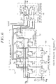
En référence à la figure 1, un convertisseur parallèle-série selon la technique antérieure reçoit des données DE sous forme de mots ayant chacun M bits parallèles, d'un équipement de traitement numérique distant EQ dans un bus d'entrée BSO à M fils et produit en sortie ces données sous forme sérialisée dans un support de transmission ST. Le convertisseur connu comprend typiquement une base de temps 1, un dispositif de rephasage 2, un registre parallèle-parallèle 3 et un registre parallèle-série 4.With reference to FIG. 1, a parallel-serial converter according to the prior art receives data DE in the form of words each having M parallel bits, from remote digital processing equipment EQ in an input bus BS O to M wires and outputs this data in serialized form in an ST transmission medium. The known converter typically comprises a
La base de temps 1 reçoit un signal d'horloge de traitement série H à une première fréquence F et produit un signal de chargement LOAD et un signal d'horloge de traitement parallèle HM à une seconde fréquence F/M, M désignant le nombre de fils du bus d'entrée BSO du convertisseur parallèle-série. Les signaux H et LOAD sont appliqués à deux entrées respectives du registre parallèle/série 4. Le signal d'horloge HM est appliqué à une entrée du dispositif de rephasage 2 et est transmis à l'équipement de traitement distant EQ en tant que signal d'horloge de référence. Compte-tenu de ce signal d'horloge de référence HM , l'équipement de traitement distant dispose d'une fréquence (F/M) et d'une phase de référence pour transmettre à ladite fréquence, des mots de données DE à M bits parallèles dans le bus BSO, l'entier M étant typiquement égal à huit. En fonction des mots de données reçus et du signal d'horloge HM, le dispositif 2 produit un signal d'horloge corrigé HC afin d'échantillonner correctement le signal de données. Ce signal HC résulte d'une correction de phase du signal d'horloge HM qui dépend de la distance séparant l'équipement de traitement distant EQ du convertisseur et introduisant un déphasage des données entrantes DE par rapport au signal d'horloge locale de traitement parallèle HM.The
Le signal d'horloge corrigé HC est appliqué à une entrée d'horloge du registre parallèle-parallèle 3 qui reçoit également, à travers un bus de sortie à M fils BS1 du dispositif de rephasage 2, les mots de données entrantes DE. Dans le registre 3, les mots de données DE sont transférés au rythme du signal HC, via un bus de sortie à M fils BS2, à des entrées de données du registre parallèle-série 4. Le signal de chargement LOAD commande le chargement des M bits de chacun des mots de données présent dans le bus BS2 dans M cellules de mémoire tampon du registre parallèle-série 4. Ces bits de mot mémorisés sous forme parallèle dans le registre parallèle-série 4 sont ensuite lus un à un sous la commande du signal d'horloge de traitement série H pour être transmis sous forme sérialisée dans le support de transmission ST. Le signal de chargement LOAD est un signal impulsionnel périodique dont la largeur temporelle des impulsions est égale à une période du signal d'horloge de traitement série H, et dont la période est égale à M périodes de ce signal d'horloge H.The corrected clock signal HC is applied to a clock input of the parallel-
Il apparaît, selon cette réalisation connue, que des fronts montants du signal d'horloge corrigé HC seront positionnés de façon "pseudo-aléatoire" par rapport aux fronts montants des impulsions du signal de chargement LOAD. Par conséquent la stabilité des données lors d'une phase de transfert entre registres 3 et 4 n'est pas garantie, et peut entraîner une perte de données.It appears, according to this known embodiment, that rising edges of the corrected clock signal HC will be positioned in a "pseudo-random" manner relative to the rising edges of the pulses of the LOAD loading signal. Consequently, the stability of the data during a transfer phase between
Par ailleurs, une gigue de phase peut être a priori présente dans les données entrantes DE. Cette gigue provoque des changements de la phase du signal d'horloge corrigé HC, entraînant des transferts entre registres 3 et 4 à des instants variables imprévisibles qui sont néfastes au fonctionnement du convertisseur.Furthermore, a phase jitter may be a priori present in the incoming data DE. This jitter causes signal phase changes of clock corrected HC, causing transfers between
Le premier inconvénient évoqué ci-dessus résulte d'une indépendance du signal d'horloge corrigé HC par rapport à une quelconque référence temporelle, contrairement au signal de chargement LOAD fourni par la base de temps locale 1. Un glissement de l'une des phases des signaux HC et LOAD par rapport à l'autre est ainsi engendré.The first drawback mentioned above results from an independence of the clock signal corrected HC with respect to any temporal reference, contrary to the loading signal LOAD provided by the
La figure 2 montre en détail une réalisation connue du dispositif de rephasage 2 inclus dans le convertisseur de la figure 1. Le dispositif de rephasage 2, appelé également "phaseur", comprend un circuit de détection de transition et de calcul d'adresse 21, un circuit d'échantillonnage 22, un circuit de retard 23 et un multiplexeur N-vers-1 24.FIG. 2 shows in detail a known embodiment of the
Le circuit de retard 23 est constitué de N lignes à retard 231 à 23N de retard élémentaire Td, connectées en série. Le signal d'horloge de traitement parallèle HM produit par la base de temps 1 est appliqué à une entrée de la première ligne à retard 231, et chacune 23n des lignes à retard 231 à 23N reproduit en sortie ce signal d'horloge HM retardé de (n.Td), avec 1 ≤ n ≤ N. Ainsi le signal d'horloge HM est retardé par des multiples d'un retard élémentaire Td aux sorties respectives des lignes à retard 231 à 23N, en une pluralité de signaux d'horloge déphasés. Ces signaux d'horloge déphasés sont appliqués, d'une part, à N entrées du multiplexeur 24 et, d'autre part, à N entrées d'horloge du circuit d'échantillonnage 22, respectivement.The
Le circuit d'échantillonnage 22 est constitué de N bascules de type D 221 à 22N recevant chacune par son entrée de données D l'un des bits parallèles des mots de données entrantes DE reçu à travers l'un des M fils du bus BSO , et noté DEO . Aux entrées d'horloge des bascules 221 à 22N sont respectivement appliqués les signaux d'horloge déphasés produits aux sorties des lignes à retard 231 à 23N. Des sorties Q des bascules 221 à 22N sont appliquées à des entrées respectives du circuit de détection de transition et de calcul d'adresse 21. Dans les bascules 221 à 22N, le bit de données entrantes DEO est échantillonné respectivement à des instants Td, (2.Td),..., (N.Td) succédant à un front montant du signal HM. Les sorties Q des bascules sont représentatives sous forme discrète de l'état logique, "1" ou "0", du bit de données entrantes DEO aux différents instants d'échantillonnage successifs respectifs. En choisissant convenablement le retard Td imposé par chacune des lignes à retard 231 à 23N, les sorties Q des bascules indiquent la localisation temporelle d'un front montant ou descendant du bit, et plus généralement des transitions dans le signal de données DE. Ainsi par exemple des niveaux "1" et "0" produits respectivement aux sorties des bascules 211 à 21i et 21i+1 à 21N, où i dénote un indice entier quelconque compris entre 1 et N, identifient la localisation d'un front descendant du signal DEO et donc d'une transition logique pour chacun des bits du signal DE, en correspondance de phase sensiblement avec le front montant du signal d'horloge déphasé produit à la sortie de la ième ligne à retard 23i.The
En fonction des états des sorties Q des bascules dans le circuit d'échantillonnage 22, le circuit 21 établit une adresse adi qui correspond à l'indice de la bascule 21i selon l'exemple ci-dessus. L'adresse adi est appliquée à des entrées de sélection ES du multiplexeur 24 afin de sélectionner le signal d'horloge déphasé produit par la ligne à retard 23i parmi les N signaux d'horloge déphasés de manière à produire le signal d'horloge corrigé HC en sortie du multiplexeur 24.As a function of the states of the outputs Q of the flip-flops in the
Le diagramme temporel de la figure 3 est relatif au fonctionnement envisagé d'un convertisseur parallèle-série selon l'invention. Dans ce diagramme, il est supposé que les données entrantes parallèles DE dans le bus BSO sont des mots à M=8 bits parallèles. L'inconvénient principal inhérent au convertisseur parallèle-série selon la technique antérieure présenté ci-dessus réside dans le fait que le signal d'horloge corrigé en phase HC, dont les fronts montants provoquent des transferts de données du bus BS1 vers le bus BS2, est indépendant du signal de chargement LOAD des données du bus BS2 dans le registre parallèle-série 4. Selon l'invention, à la fois le signal de chargement LOAD, représenté sur une troisième ligne de la figure 3, et un signal d'horloge HM' , montré sur une quatrième ligne, sont produits par une même base de temps locale incluse dans le convertisseur. Ce signal d'horloge HM' de période M/F, égale à une durée de temps-mot des données entrantes DE, offre des fronts montant et descendant sensiblement compris entre deux impulsions du signal de chargement LOAD. En fonction de la phase des données entrantes, est sélectionné, ou bien le signal d'horloge HM' , ou bien le signal complémentaire de celui-ci, noté ![]()
![]()
En référence à la figure 4, un convertisseur parallèle-série selon l'invention comprend une base de temps 1a, un inverseur logique 11a, les deux registres parallèle-parallèle et parallèle-série 3 et 4, un circuit d'analyse de phase 5 et un commutateur électronique 6.With reference to FIG. 4, a parallel-series converter according to the invention comprises a time base 1a, a
La base de temps 1a reçoit un signal d'horloge de traitement série H ayant une fréquence F, et produit un signal de chargement LOAD, qui est appliqué à une entrée de chargement du registre parallèle-série 4, et des premier et second signaux d'horloge de traitement parallèle HM et HM'. Le premier signal HM est appliqué à une entrée du circuit d'analyse 5 et est également transmis à un équipement de traitement numérique distant EQ afin que ce dernier transmette à la fréquence du signal HM des mots de données ayant chacun M bits parallèles dans un bus BSO connecté à des entrées du circuit 5.The time base 1a receives a processing clock signal series H having a frequency F, and produces a loading signal LOAD, which is applied to a loading input of the parallel-
Le second signal d'horloge de traitement parallèle HM' , sensiblement déphasé par rapport au signal HM pour des raisons explicitées ultérieurement, est appliqué à deux entrées du commutateur 6, respectivement directement et à travers l'inverseur 11a. Le second signal d'horloge de traitement parallèle HM' et un second signal d'horloge de traitement parallèle complémentaire ou inversé ![]()
![]()
![]()
![]()
En revenant à la figure 3, il apparaît qu'une condition nécessaire au bon fonctionnement du convertisseur parallèle-série selon l'invention consiste en ce que des fronts montants des impulsions du signal de chargement LOAD ayant une largeur égale à une période du signal d'horloge H et délivrées toutes les M périodes du signal d'horloge H doivent succéder chacun de manière sensible à des fronts montant et descendant successifs dans le second signal d'horloge de traitement parallèle HM', sachant qu'un front descendant du signal HM' correspond à un front montant du signal complémentaire ![]()
![]()
Dans les réalisations décrites ci-après du circuit d'analyse de phase 5 inclus dans le convertisseur parallèle-série selon l'invention, l'entier M est supposé égal à 8. Ainsi les données parallèles entrantes DE sont transmises sous forme de mots à 8 bits parallèles dans le bus BSO. Un mot de données entrantes DE s'écrit donc sous la forme d'un octet (DEO , DE1 , DE2 , DE3 , DE4 , DE5 , DE6 , DE7=DEM-1).In the embodiments described below of the
En référence à la figure 6, le circuit d'analyse de phase 5 comprend un circuit de mémorisation 51, un circuit d'échantillonnage 52, un circuit de retard 53 et un circuit logique de génération de signal de commande 54. Seul, par exemple l'un des bits dans les mots de données entrantes DE, à savoir le bit de poids faible DEO, est utilisé en tant que signal de bit prédéterminé par le circuit d'analyse 5 du convertisseur selon l'invention, bien que n'importe lequel des bits dans un mot de données à M=8 bits parallèles transmis par le bus d'entrée BSO peut être utilisé puisque tous les bits d'un mot dans les fils respectifs du bus BSO présentent des phase et débit strictement identiques.With reference to FIG. 6, the
Le circuit de retard 53 est constitué par exemple de trois lignes à retard 531, 532 et 533 en série dont la première reçoit le signal de bit prédéterminé DEO de chacun des mots de données entrantes DE. Chaque ligne à retard, 531 à 533, retarde d'un retard élémentaire Td prédéterminé le bit qu'elle reçoit. Aux sorties des trois lignes à retard 531 à 533, sont donc obtenus des signaux de bit de poids faible retardés, c'est-à-dire déphasés respectivement par des multiples d'un déphasage élémentaire (2π.Td / T M ) où TM=M/F est la période des mots de données entrantes. Le signal de bit de poids faible DEO et les signaux déphasés issus des lignes à retard 531 à 533 sont respectivement appliqués aux entrées d'horloge de quatre bascules de type D, 521, 522, 523 et 524 constituant le circuit d'échantillonnage 52.The
Les bascules 521 à 524 reçoivent chacune par leur entrée de données D, le premier signal d'horloge HM. Dans ces différentes bascules 521 à 524, le premier signal d'horloge HM est échantillonné par les signaux déphasés de phases différentes, en réponse à chacun des fronts montants du signal de bit de poids faible non déphasé (non retardé) DEO. Quatre états logiques résultant de l'échantillonnage du premier signal d'horloge HM en fonction des différentes phases successives sont ainsi fournis respectivement par les sorties Q des quatre bascules 521 à 524 du circuit d'échantillonnage 52. Les sorties Q des quatre bascules 521 à 524 sont appliquées respectivement aux entrées de données D de bascules de type D 511 , 512 , 513 et 514 dans le circuit de mémorisation 51. L'entrée d'horloge de chaque bascule 511 à 514 reçoit le signal de bit prédéterminé DEO. Ainsi en réponse à un front montant du signal DEO , les états logiques du premier signal d'horloge HM échantillonnés par les différents signaux déphasés sont stabilisés dans le circuit 51 et reproduits en synchronisme avec le front montant suivant du signal DEO aux sorties Q des bascules 511 à 514. Les sorties directes Q et inverses ![]()
![]()
![]()
![]()
![]()
![]()
![]()
![]()
Avant de revenir en détail sur le circuit de génération de signal de commande 54, il est maintenant fait référence aux figures 5 et 7 pour décrire le fonctionnement du circuit d'analyse de phase 5.Before returning in detail to the control
Le diagramme temporel montré à la figure 5 concerne la scrutation du signal HM par le circuit d'échantillonnage 52. Une troisième ligne de ce diagramme temporel montre le premier signal d'horloge HM qui est appliqué à chacune des entrées de données D des bascules 521 à 524 du circuit d'échantillonnage 52. Des quatrième, cinquième, sixième et septième lignes montrent respectivement le signal de bit de poids faible DEO des données entrantes et les signaux résultant du déphasage ou retard du signal DEO aux sorties des trois lignes à retard 531 à 533.The time diagram shown in FIG. 5 relates to the scanning of the signal H M by the
Les fronts montants de chacun de ces signaux constituent des instants d'échantillonnage du premier signal d'horloge HM dans les bascules 521 à 524. Ces différents instants d'échantillonnage successifs sont contenus dans une durée d'analyse de phase Ta, égale à 3.Td, du premier signal d'horloge HM . Notamment ces différents instants d'échantillonnage du premier signal d'horloge HM permettent de "repérer" des débuts de temps-mot (fronts montants) des données entrantes relativement à des fronts montants ou descendants du premier signal d'horloge HM afin de sélectionner soit le second signal d'horloge HM' , soit le second signal d'horloge inversé ![]()
- d'une part, pour assurer le transfert des données entrantes DE dans le bus BS2, doit être sélectionné celui des deux signaux d'horloge, HM' et

- d'autre part pour prélever et mémoriser des mots de données présents dans le bus BS2, le signal de chargement LOAD du registre parallèle-
série 4 doit présenter des fronts montants d'échantillonnage relativement éloignés temporellement des fronts montants des signaux d'horloge HM' et

- on the one hand, to ensure the transfer of the incoming data DE on the bus BS 2 , must be selected that of the two clock signals, H M 'and
- on the other hand to take and store data words present in the bus BS 2 , the LOAD loading signal of the parallel-
series register 4 must have rising edges of sampling relatively distant in time from the rising edges of the clock signals H M 'and
En se référant à la figure 5 et en considérant en outre la première condition précitée, deux informations peuvent être extraites concernant la durée d'analyse Ta ou, ce qui est équivalent, la somme des retards élémentaires Td imposés par les lignes à retard 531 à 533. Tout d'abord, cette durée d'analyse Ta doit être inférieure à la moitié de la période du premier signal d'horloge HM afin de détecter au maximum un seul front, montant ou descendant, dans ce signal d'horloge HM , la détection d'un seul front étant suffisante pour "repérer" la phase des mots de données entrantes relativement au signal d'horloge HM. Par ailleurs cette durée d'analyse Ta doit être supérieure à un temps minimal de prépositionnement des mots de données entrantes DE sur les entrées du registre parallèle-parallèle 3. Sans cela, il ne serait pas possible de "repérer" dans une plage de temps suffisamment grande la phase des mots de données entrantes DE relativement au signal d'horloge HM et ainsi assurer de manière certaine que des débuts de temps-mot des mots de données entrantes DE ne sont pas situés au voisinage de fronts montants de l'un des deux signaux d'horloge HM' et ![]()
![]()
Le diagramme temporel de la figure 7 vise à établir une correspondance entre les différents états d'échantillonnage pouvant être produits aux sorties des bascules 511 à 514 du circuit de mémorisation 51 et le signal d'horloge HM' ou ![]()
![]()
Il est à noter que l'un HM' des deux seconds signaux d'horloge est sensiblement en avance de phase par rapport au premier signal d'horloge HM et l'autre second signal d'horloge ![]()
![]()
![]()
![]()
Une cinquième ligne dans la figure 7 montre que, dans le cas où un front descendant du signal HM est détecté lors des échantillonnages successifs par le signal DEO retardé, le second signal d'horloge HM' doit être sélectionné pour échantillonner les données parallèles entrantes pour leur transfert dans le bus BS2 .A fifth line in FIG. 7 shows that, in the case where a falling edge of the signal H M is detected during the successive samplings by the delayed signal DE O , the second clock signal H M 'must be selected to sample the data incoming parallels for their transfer in the bus BS 2 .
Volontairement, deux cas particuliers n'ont pas été traités ci-dessus savoir les cas où ni le front montant, ni le front descendant du premier signal d'horloge HM ne sont détectés. Ces cas correspondent au même état logique "1" ou "O" aux sorties Q de toutes les bascules 511 à 514 dans le circuit de mémorisation 51. En revenant à la figure 7 et en maintenant l'hypothèse que la durée d'analyse Ta est strictement supérieure à une durée minimale de prépositionnement de chacun des mots de données entrantes DE et est strictement inférieure à une demi-période du premier signal d'horloge HM, il est étudié ci-après le cas où toutes les bascules de mémorisation 511 à 514 mémorisent un état "1". Une telle mémorisation peut se produire lorsqu'elle succède à une mémorisation antérieure, ou bien des états "0", "1", "1" et "1" ou bien des états "1", "1", "1", "0", dans les bascules 511 à 514, respectivement en fonction du sens du glissement de la phase des données entrantes DE relativement à la phase du signal d'horloge HM.Voluntarily, two particular cases were not treated above knowing the cases where neither the rising edge, nor the falling edge of the first clock signal H M are detected. These cases correspond to the same logic state "1" or "O" at the outputs Q of all the flip-
Si les états "1", "1", "1", et "1" succèdent aux états "0", "1", "1", et "1" aux sorties des bascules 511 à 514, cela signifie en se reportant à la quatrième ligne de la figure 7, que les données entrantes DE sont alors pour ces états "1", "1", "1" et "1" sensiblement en avance de phase par rapport au temps-mot représenté en pointillé et correspondant aux états "0", "1", "1" et "1". Le signal d'horloge ![]()
![]()
Si les états "1", "1", "1" et "1" succédent aux états "1", "1", "1" et "0" cela signifie en se reportant à la cinquième ligne de la figure 7, que les mots de données entrantes DE sont alors sensiblement en retard de phase par rapport au temps-mot représenté en trait continu sur la cinquième ligne et correspondant à des états "1", "1", "1" et "O". Le second signal d'horloge HM' est alors maintenu pour échantillonner les données entrantes DE afin de les reproduire aux sorties du registre parallèle-parallèle 3.If the states "1", "1", "1" and "1" succeed to the states "1", "1", "1" and "0" this means by referring to the fifth line of FIG. 7, that the words of incoming data DE are then substantially in phase lag with respect to the time-word shown in solid line on the fifth line and corresponding to states "1", "1", "1" and "O". The second clock signal H M 'is then maintained to sample the incoming data DE in order to reproduce them at the outputs of the parallel-
Par un raisonnement identique, un résultat similaire est obtenu pour des états "0", "0", "0" et "0" mémorisés aux sorties des bascules 511 à 514 du circuit de mémorisation 51 en maintenant le second signal d'horloge HM' ou ![]()
![]()
En conséquence, une table de vérité TV est établie, comme suit :

Les secondes et troisièmes bascules 522 et 523, 512 et 513, dans les circuits 52 et 51 peuvent en pratique être suprimées, et ne sont illustrées dans la figure 6 (ou 9) que pour la compréhension du fonctionnement du circuit 5.The second and third flip-
En référence à nouveau à la figure 6, le circuit de génération de signal de commande 54 est conçu pour générer le signal CM commandant le commutateur 6 de sorte que les sorties des bascules 511 à 514 contribuent en combinaison à sélectionner le second signal d'horloge HM' ou le second signal d'horloge inversé ![]()
![]()
![]()
![]()
Le circuit de génération 54 comprend un inverseur 541, deux portes NON-ET à deux entrées 542 et 543 et une bascule RS à entrées multiples 544. La bascule RS est constituée par une porte NON-ET à trois entrées 544 et une porte NON-ET à deux entrées 545, la sortie de la porte 544 produisant le signal de commande CM. Une double entrée de mémorisation EM de la bascule RS 544 est constituée par deux entrées de la porte 544 qui sont reliées à une entrée du signal de réinitialisation RESET à travers l'inverseur 541 et à la sortie de la porte 542 dont les entrées sont reliées à la sortie Q de la bascule 511 et la sortie complémentaire ![]()
![]()
![]()
![]()
![]()
![]()
![]()
![]()
Ainsi le signal de sortie de la bascule équivalente RS, c'est-à-dire le signal de commande CM, est à l'état "1" lorsque Q1 est à l'état "1" et Q4 à l'état "O", par la fonction d'excitation S. Inversement le signal CM est à l'état "0" lorsque Q1 est à l'état "O" et Q4 est à l'état "1", par la fonction d'excitation R. Dans le cas où Q4 et Q1 sont tous deux à l'état "1" ou "0" , l'état précédent du signal CM est maintenu conformément au fonctionnement des bascules RS puisque R = S = "0". Le signal RESET est utilisé pour forcer la sortie de la bascule RS 544 et donc le signal CM à un état donné "1" lors d'une phase d'initialisation.Thus the output signal of the equivalent flip-flop RS, that is to say the control signal CM, is in state "1" when Q 1 is in state "1" and Q 4 in state "O", by the excitation function S. Conversely, the signal CM is in the state "0" when Q 1 is in the state "O" and Q 4 is in the state "1", by the function excitation R. In the case where Q 4 and Q 1 are both in the state "1" or "0", the previous state of the signal CM is maintained in accordance with the operation of the flip-flops RS since R = S = " 0 ". The RESET signal is used to force the output of the flip-
La première réalisation de convertisseur parallèle-série selon l'invention décrite précédemment particulièrement en référence aux figures 6 et 7, est de préférence utilisée lorsque sensiblement la gigue de phase n'est pas susceptible de contrarier le transfert des données entrantes.The first embodiment of a parallel-to-series converter according to the invention described above, particularly with reference to FIGS. 6 and 7, is preferably used when substantially the phase jitter is not likely to impede the transfer of the incoming data.
La seconde réalisation de convertisseur parallèle-série selon l'invention décrite ci-après , en référence aux figures 8 et 9, remédie à des effets de gigue de phase.The second embodiment of parallel-series converter according to the invention described below, with reference to FIGS. 8 and 9, remedies the effects of phase jitter.
Comme montré dans la table de vérité TV, il apparaît qu'un changement d'état du signal de commande CM, qui implique la substitution du signal d'horloge HM' au signal ![]()
![]()
La figure 8 montre sur une première ligne le premier signal d'horloge HM , tandis qu'une seconde ligne de cette figure représente, dans un cas extrême, une gigue de phase Gmax des données entrantes entraînant un saut de phase du signal sélectionné HS cadençant le registre parallèle-parallèle, ou plus précisément un changement de la sélection des deux signaux d'horloge HM et ![]()
![]()
![]()
![]()
![]()
![]()
Dans la suite, référence est faite à un exemple préféré selon lequel la durée d'analyse Ta est égale à un quart de période du signal d'horloge HM , soit Ta = TM/4. Dans cet exemple, la valeur de la gigue maximale Gmax est égale à 12 ns pour une fréquence d'horloge du signal d'horloge de traitement série H égale à 155 MHz et pour des mots de données constitués de M=8 bits, ce qui correspond à une limite supérieure de gigue de phase largement acceptable même pour des conditions extrêmes. La gigue de phase admissible est inférieure à cette gigue de phase Gmax.In the following, reference is made to a preferred example according to which the analysis time Ta is equal to a quarter period of the clock signal H M , ie Ta = T M / 4. In this example, the value of the maximum jitter G max is equal to 12 ns for a clock frequency of the serial processing clock signal H equal to 155 MHz and for data words made up of M = 8 bits, this which corresponds to an upper limit of phase jitter which is widely acceptable even under conditions extremes. The allowable phase jitter is less than this max G phase jitter.
Néanmoins, avec une gigue de phase des données entrantes inférieure à Gmax , et compte-tenu de la condition précitée sur Ta (Ta = TM/4), les sorties Q des bascules 511 à 514 peuvent basculer d'états donnés à des états suivants qui sont immédiatement adjacents dans la table de vérité TV. Plus précisément, les sorties Q des bascules 511 à 514 ne peuvent alors basculer que vers, ou bien des états immédiatement adjacents supérieurs, ou bien des états immédiatement adjacents inférieurs dans la table de vérité TV. Ainsi, à titre d'exemple, les sorties Q des bascules 511 et 514 peuvent basculer des états "0" et "0", soit en les états "0" et "1", soit en les états "1" et "0". Il a été montré, en référence à la figure 6, qu'un signal RESET force, lors de l'initialisation du convertisseur, la sortie de la bascule RS 544 et donc le signal de commande CM à un état "1". Or il est possible que, suite à cette étape de réinitialisation, les états de sortie "naturels" initiaux des bascules 511 et 514 soient "0" et "0", ou "1" et "1" (table de vérité), et maintiennent ainsi le signal de commande CM à l'état "1". Mais il a été vu précédemment que la gigue de phase G des données entrantes DE peut provoquer un basculement d'états donnés des bascules 511 et 514 en des états immédiatement adjacents supérieurs ou inférieurs.Nevertheless, with a phase jitter of the incoming data less than G max, and taking into account the aforementioned condition on Ta (Ta = T M / 4), the outputs Q of the flip-
Ainsi, en référence à la table de vérité TV, les états "0" et "0", ou "1" et "1", mémorisés respectivement aux sorties des bascules 511 et 514 , et correspondant à un état "1" du signal de commande CM suite à la réinitialisation (RESET = "1") du convertisseur, peuvent basculer en les états "0" et "1". Le signal de commande CM prend alors l'état "0", en imposant un changement de phase du signal d'horloge sélectionné HS après la réinitialisation, changement de phase très néfaste au fonctionnement du convertisseur et pouvant entraîner des pertes de données. En supposant maintenant qu'immédiatement après l'initialisation du signal de commande CM à l'état "1" par le signal RESET, le signal de commande CM bascule à l'état "0" lors d'une augmentation de la gigue de phase G, alors le signal CM ne peut plus ensuite rebasculer à l'état "1", puisque comme signalé ci-dessus, compte tenu des conditions sur la gigue de phase G (G<Gmax) et sur la durée d'analyse Ta, les états des sorties des bascules 511 à 514 ne peuvent basculer que d'états donnés à des états immédiatement adjacents, supérieurs ou inférieurs, en référence à la table de vérité TV, par excursion positive et négative de la gigue de phase.Thus, with reference to the truth table TV, the states "0" and "0", or "1" and "1", stored respectively at the outputs of flip-
Le problème de la gigue de phase ne se pose donc que si la sortie "naturelle" initiale de la bascule RS 544 produisant le signal de commande CM prend un état "1" identique à l'état auquel la bascule RS est initialement forcée lors de l'initialisation par le signal RESET. Plus précisément, ce problème de gigue de phase se pose si les sorties des bascules 511 et 514 prennent des états "1", "1" ou "0", "0" en maintenant le signal de commande CM à l'état "1". Dans ce cas en effet, la gigue de phase peut faire basculer les sorties des bascules 511 à 514 en des états immédiatement adjacents, soit "0" et "1" pour les bascules 511 et 514, entraînant un changement de phase du signal d'horloge sélectionné HS. Il faut noter cependant que, si la gigue du signal de données est inférieure à la gigue de phase maximale Gmax , ce saut de phase ne se produira qu'une fois.The problem of phase jitter therefore only arises if the initial "natural" output of the flip-
La figure 9 montre une seconde réalisation d'un circuit d'analyse de phase 5A inclus dans un convertisseur parallèle-série selon l'invention et résolvant ce problème de gigue de phase. Le circuit 5A comprend le circuit de mémorisation 51, le circuit d'échantillonnage 52, le circuit de retard 53 et le circuit de génération de signal de commande 54 identiques à et agencés de la même manière que ceux dans le circuit précédent 5 montré à la figure 6. Le circuit d'analyse de phase 5A comporte, en outre, un circuit d'initialisation de signal de commande 55. Ce circuit 55 comprend deux lignes à retard 5511 et 5512 connectées en cascade et imposant chacune un retard élémentaire Tr, un multiplexeur 4-vers-1 552, un compteur synchrone à 2 bits 553 constitué de deux bascules de type D 5531 et 5532 , une porte NON-ET à deux entrées 554 et une porte ET à deux entrées 552.FIG. 9 shows a second embodiment of a phase analysis circuit 5A included in a parallel-series converter according to the invention and solving this problem of phase jitter. The circuit 5A comprises the
Quatre entrées EO, E1, E2, et E3 du multiplexeur 552 reçoivent le signal relatif à l'un prédéterminé des fils du bus d'entrée de convertisseur, par exemple celui correspondant au signal de bit de poids faible DEO des mots de données à M bits parallèles DE, respectivement à travers la première ligne à retard 5511 , à travers les deux lignes à retard 5511 et 5512 , directement, et à travers la première ligne à retard 5511. Deux entrées d'adresse AD du multiplexeur 552 sont reliées à deux sorties respectives Q du compteur 553 et sélectionnent respectivement les entrées EO, E1, E2 et E3 lorsque AD="OO", "1O", "11" et "O1". Une sortie S du multiplexeur 552 est appliquée à l'entrée de la première ligne à retard 531 dans le circuit de retard 53, à l'entrée d'horloge de la première bascule 521 dans le circuit d'échantillonnage 52 et aux entrées d'horloge des bascules 511 à 514 dans le circuit de mémorisation 51, comme y est appliqué directement le signal de bit prédéterminé DEO dans le circuit 5 montré à la figure 6.Four inputs E O , E 1 , E 2 , and E 3 of the
Les deux entrées de la porte 554 sont connectées respectivement à la sortie de données Q de la bascule 5532 et la sortie de données complémentaires ![]()
![]()
![]()
![]()
Comme évoqué précédemment, le circuit d'initialisation du signal de commande 55 est destiné à positionner le signal de commande CM à un état stable définitif lors de l'étape d'initialisation du convertisseur.As mentioned above, the initialization circuit of the
Lors de l'étape d'initialisation, le signal de réinitialisation RESET commande la mise à zéro, "0" et "0", des sorties Q du compteur 553. Trois fronts montants successifs du signal de bit prédéterminé DEO mettent respectivement les sorties Q des bascules 5531 et 5532 dans ce compteur aux états "1" et "0" puis, "1" et "1" puis "0" et "1". Ces deux derniers états "0" et "1" du compteur 553 ne sont alors plus modifiés puisque la sortie de la porte NON-ET 554 est à l'état "0" qui ne valident pas, à travers la porte fermée ET 555, le signal de bit prédéterminé DEO.During the initialization step, the reset signal RESET commands the zero outputs, "0" and "0", of the outputs Q of the
Pour ces quatre couples d'états successifs aux sorties Q du compteur 553, les entrées EO , E1 , E2 et E3 sont respectivement sélectionnées en sortie S du multiplexeur 552. Ainsi successivement, les signaux DEO respectivement retardé de Tr, puis retardé de 2Tr, puis non retardé et enfin à nouveau retardé de Tr sont sélectionnés en sortie S du multiplexeur 552.For these four pairs of successive states at the outputs Q of the
Le retard Tr est sensiblement pris égal à la gigue maximale crête Gmax supportée par le convertisseur.The delay Tr is substantially taken equal to the maximum peak jitter G max supported by the converter.
L'utilisation des deux lignes à retard 5511 et 5512 constitue un moyen d'étudier le comportement du convertisseur en présence de gigue de phase pour des excursions positive et négative maximales de cette gigue de phase autour d'une phase moyenne du signal de bit prédéterminé DEO déterminée par la phase du signal DEO, alors retardé de Tr par la ligne à retard 5511.The use of the two delay lines 551 1 and 551 2 constitutes a means of studying the behavior of the converter in the presence of phase jitter for maximum positive and negative excursions of this phase jitter around an average phase of the signal. predetermined bit DE O determined by the phase of the signal DE O , then delayed by Tr by the delay line 551 1 .
Comme signalé précédemment dans la description, si la gigue de phase G est inférieure à la gigue de phase maximale Gmax , alors lors de ces deux changements de phase par des excursions positive et négative de la gigue de phase, le signal de commande CM garde ou prend un état stable définitif et donc l'horloge sélectionnée HS ne subit par la suite aucun changement de phase.As indicated previously in the description, if the phase jitter G is less than the maximum phase jitter G max , then during these two phase changes by positive and negative excursions of the phase jitter, the control signal CM keeps or takes a definitive stable state and therefore the selected clock HS does not subsequently undergo any phase change.
En sachant que lors de l'initialisation, le signal RESET force le signal de commande CM à l'état "1", pour sélectionner ainsi le signal d'horloge HM' , deux cas peuvent se produire lors de cette initialisation. Si lors des excursions positive et négative de la phase du signal de données d'entrée de part et d'autre d'une phase de signal DEO retardé de Tr, le signal de commande CM est maintenu à l'état "1", alors cet état est définitif. Si lors de ces excursions, le signal CM bascule à l'état "0", ce qui correspond à des états "1" et "1", ou "0" et "0", mémorisés aux sorties des bascules 511 et 514 respectivement suite à l'application du signal RESET et avant les excursions positive et négative de la gigue de phase du signal de bit prédéterminé DEO, alors cet état "0" est définitivement maintenu pour le signal de commande CM, et le signal d'horloge ![]()
![]()
Comme signalé précédemment, la gigue de phase maximale Gmax admissible par le convertisseur parallèle-série selon l'invention est directement fonction de la durée d'analyse Ta égale à la somme des trois retards Td imposés par les lignes à retard 531 à 533 du circuit de retard 53.As previously indicated, the maximum phase jitter G max admissible by the parallel-series converter according to the invention is directly a function of the analysis time Ta equal to the sum of the three delays Td imposed by the
Selon une première variante, chacune de ces lignes à retard est réalisée par une chaîne d'inverseurs en cascade et en nombre pair. Chaque inverseur produit un retard fonction des dimensions des transistors qui le compose.According to a first variant, each of these delay lines is produced by a chain of inverters in cascade and in even number. Each inverter produces a delay depending on the dimensions of the transistors which compose it.
Selon une seconde variante montrée à la figure 1O, le circuit de retard 53 est constitué de plusieurs bascules de type D ,BA, connectées en cascade. L'entrée de données de la première bascule BA1 reçoit le signal de bit prédéterminé DEO selon la figure 6, ou le signal en sortie S du multiplexeur 552 selon la figure 9. La sortie Q de chacune des autres bascules est reliée à l'entrée D de la bascule suivante respective. Chacune des lignes à retard 531 à 533 peut être constituée par une ou plusieurs bascules dont le nombre dépend de la durée d'analyse Ta et du nombre de bits M dans les mots de données DE, c'est-à-dire du rapport M entre la fréquence du signal d'horloge de bit H et de la fréquence des signaux d'horloge de mots HM et HS. Les entrées d'horloge des bascules BA reçoivent, alternativement une sur deux, respectivement le signal d'horloge de traitement série H et le signal complémentaire ![]()
![]()
A titre d'exemple, la figure 1O illustre un circuit de retard 53 composé de deux lignes à retard 531 et 533 imposant chacune un retard Td égal à une demi-période du signal d'horloge H, et comprenant chacune deux bascules BA1 et BA2, BA3 et BA4 afin de conférer une durée d'analyse de phase Ta égale à une période et demi du signal H.By way of example, FIG. 10 illustrates a
Claims (12)
- Parallel-to-serial converter receiving incoming data words (DE) each having M parallel bits (DE0 to DEM-1) from a digital processing device (EQ) for converting them into serialized bits transmitted at a first frequency (F) in a transmission medium (ST), said converter comprisinga time base (1a), a parallel-to-parallel register (3) and a parallel-to-serial register (4),said time base (1a) receiving a clock signal (H) at said first frequency (F) and producing a loading clock signal (LOAD) at a second frequency (F/M) M times less than said first frequency (F) to rhythm the loading of the data words with parallel bits (DE), which are previously transferred to outputs of the parallel-to-parallel register (3), into the parallel-to-serial register (4), and a first clock signal (HM) at said second frequency transmitted to said digital processing device to synchronize it,characterized in thatsaid time base (1a) further products two second clock signals (HM',
 and that said converter further comprises a phase analysing means (5) for analysing the phase of said incoming data words with parallel bits (DE) compared to the phase of said first clock signal (HM) in order to select one of said two second clock signals (HM',
- Parallel-to-serial converter according to claim 1, characterized in that said first clock signal (HM) and one of said two second clock signals (HM',

- Parallel-to-serial converter according to claim 1 or 2, characterized in that loading times of said parallel-to-serial register (4) determined by the loading clock signal (LOAD) occur periodically substantially after transfer times of the incoming data words determined by any one of said two second clock signals (HM.,

- Parallel-to-serial converter according to any one of claims 1 to 3, characterized in that the time base (1a) produces one of said two second clock signals (HM') directly, and the other (

- Parallel-to-serial converter according to any one of claims 1 to 4, characterized in that said phase analysing means (5) comprises:several cascade-connected delay means (531, 532, 533) imposing delays the sum of which defines a predetermined phase analysis duration (Ta), for delaying predetermined one (DE0) of M bit signals relative to the M parallel bits in said incoming data words (DE) in several delayed signals, respectively, said analysis duration (Ta) being less than a half-period of said clock signals (HM, HM',
 several sampling means (521, 522, 523, 524) for sampling said first clock signal (HM) in response to predetermined logic transitions ("0" to "1") of said predetermined bit signal (DE0) and said delayed signals in order to produce several sampling signals (Q, 52) respectively, anda logic means (54) for generating as a function of two (Q1, Q4) of said several sampling signals, a control signal (CM) whose two logic states select said two second clock signals (HM',
- Parallel-to-serial converter according to claim 5, characterized in that it comprises a switching means (6) receiving said second clock signals (HM',


- Parallel-to-serial converter according to claim 5 or 6, characterized in that said phase analysing means (5) further comprises
several storing means (511, 512, 513, 514) connected between said several sampling means and said logic means for storing logic states of said sampling state signals (Q, 52) produced respectively by said several sampling means (521, 522, 523, 524) for a duration of transmission of one incoming data word with parallel bits (DE). - Parallel-to-serial converter according to any one of claims 5 to 7, characterized in thatsaid two sampling signals (Q1, Q4) result from sampling of said first clock signal (HM) by said predetermined bit signal (DE0) and a most delayed of said several delayed signals, andsaid logic means (54) comprises a first input means (542) responsive to one (Q1) of said two sampling signals and to a signal inverted with respect to the other (Q4) of said two sampling signals so that the logic means generates an initial logic state (CM = "1") of said control signal selecting one (HM') of said two second clock signals, and a second input means (543) responsive to said other (Q4) of said two sampling signals and to a signal inverted with respect to said one (Q1) of said two sampling signals so that said logic means generates a second logic state (CM = "0") of said control signal selecting the other (

- Parallel-to-serial converter according to any one of claim 5 to 8, characterized in thatsaid phase analysing means (5A) further comprises a means (541, RESET) for forcing the control signal (CM) into a forced signal at a given state ("1") selecting one (
 said predetermined bit signal (DE0) is received through a control signal initiating means (55) to initiate to a stable definitive state during said initial stage, said forced control signal independently of any phase jitter in the incoming data words (DE) less than a maximal phase jitter (Gmax).
 - Parallel-to-serial converter according to claim 9, characterized in that the maximal phase jitter (Gmax) is substantially equal to the difference between the half-period of said clock signals (HM, HM',

- Parallel-to-serial converter according to claim 9 or 10, characterized in that said initiating means (55) comprises first and second delay means connected in cascade (5511, 5512) receiving said predetermined bit signal (DE0) to produce first and second delayed signals, respectively, and a means (552, 553) for selecting during said initial stage, successively the first delayed signal by the first delay means (5511), then the second delayed signal by the first and second delay means (5511, 5512), then said predetermined bit signal, and finally said first delayed signal, each of said first and second delay means imposing a delay (Tr) substantially equal to the maximal phase jitter (Gmax).
- Parallel-to-serial converter according to any one of claims 5 to 11, characterized in that each of said several cascade-connected delay means (531, 532, 533) comprises at least one flip-flop (BA), said flip-flops (BA1 - BA4) being connected in cascade and having clock inputs receiving alternately, one out of two, said clock signal (H) at the first frequency and a signal (

Applications Claiming Priority (2)
| Application Number | Priority Date | Filing Date | Title |
|---|---|---|---|
| FR9208940 | 1992-07-20 | ||
| FR929208940A FR2693860B1 (en) | 1992-07-20 | 1992-07-20 | Parallel-to-serial converter. |
Publications (2)
| Publication Number | Publication Date |
|---|---|
| EP0580234A1 EP0580234A1 (en) | 1994-01-26 |
| EP0580234B1 true EP0580234B1 (en) | 1996-09-11 |
Family
ID=9432063
Family Applications (1)
| Application Number | Title | Priority Date | Filing Date |
|---|---|---|---|
| EP93202096A Expired - Lifetime EP0580234B1 (en) | 1992-07-20 | 1993-07-16 | Parallel-serial converter |
Country Status (5)
| Country | Link |
|---|---|
| US (1) | US5319369A (en) |
| EP (1) | EP0580234B1 (en) |
| JP (1) | JPH06224781A (en) |
| DE (1) | DE69304632T2 (en) |
| FR (1) | FR2693860B1 (en) |
Families Citing this family (22)
| Publication number | Priority date | Publication date | Assignee | Title |
|---|---|---|---|---|
| JPH07203335A (en) * | 1993-12-28 | 1995-08-04 | Mitsubishi Electric Corp | Rotary device |
| FR2727587A1 (en) * | 1994-11-30 | 1996-05-31 | Sgs Thomson Microelectronics | HIGH-THROUGHPUT BINARY DATA SERIALIZATION DEVICE |
| US5721545A (en) * | 1995-10-23 | 1998-02-24 | Poplevine; Pavel B. | Methods and apparatus for serial-to-parallel and parallel-to-serial conversion |
| US5757297A (en) * | 1996-06-07 | 1998-05-26 | International Business Machines Corporation | Method and apparatus for recovering a serial data stream using a local clock |
| JP3394159B2 (en) * | 1997-06-27 | 2003-04-07 | 株式会社リコー | Interface circuit for serial DA converter |
| US6269135B1 (en) * | 1998-01-14 | 2001-07-31 | Tropian, Inc. | Digital phase discriminations based on frequency sampling |
| US5982309A (en) * | 1998-01-09 | 1999-11-09 | Iowa State University Research Foundation, Inc. | Parallel-to-serial CMOS data converter with a selectable bit width mode D flip-flop M matrix |
| DE19917016A1 (en) * | 1999-04-15 | 2000-10-19 | Philips Corp Intellectual Pty | Circuit for conversion of parallel data stream into series one and vice versa and for intermediate storage and clocked transmission of data stream |
| US6340899B1 (en) * | 2000-02-24 | 2002-01-22 | Broadcom Corporation | Current-controlled CMOS circuits with inductive broadbanding |
| US6614371B2 (en) * | 2001-07-19 | 2003-09-02 | Broadcom Corporation | Synchronous data serialization circuit |
| US6690223B1 (en) * | 2001-12-27 | 2004-02-10 | Bay Microsystems, Inc. | System and method for shifting the phase of a clock signal |
| US6925575B2 (en) * | 2002-04-05 | 2005-08-02 | Intel Corporation | Selectable clocking synchronization of a parallel-to-serial converter and memory |
| US7197053B1 (en) * | 2003-03-05 | 2007-03-27 | Applied Micro Circuits Corporation | Serializer with programmable delay elements |
| US6756925B1 (en) * | 2003-04-18 | 2004-06-29 | Northrop Grumman Corporation | PSK RSFQ output interface |
| TWI266485B (en) * | 2005-02-18 | 2006-11-11 | Realtek Semiconductor Corp | Multi-phase clock generator and generating method for network controller |
| DE102008029458B4 (en) * | 2008-06-20 | 2019-02-07 | Carl Zeiss Microscopy Gmbh | Method for recording pulse signals |
| KR20130082303A (en) * | 2012-01-11 | 2013-07-19 | 한국전자통신연구원 | Serializer |
| US9525573B2 (en) | 2015-01-23 | 2016-12-20 | Microsoft Technology Licensing, Llc | Serializing transmitter |
| US9432061B2 (en) | 2015-01-23 | 2016-08-30 | Microsoft Technology Licensing, Llc | Serializing transmitter |
| US9698792B1 (en) * | 2016-11-22 | 2017-07-04 | Nxp B.V. | System and method for clocking digital logic circuits |
| CN110011669A (en) * | 2019-04-15 | 2019-07-12 | 上海安路信息科技有限公司 | A kind of data converter |
| CN116137535B (en) * | 2023-02-09 | 2023-08-29 | 上海奎芯集成电路设计有限公司 | Parallel-to-serial conversion circuit and method for generating parallel-to-serial conversion clock signal |
Family Cites Families (5)
| Publication number | Priority date | Publication date | Assignee | Title |
|---|---|---|---|---|
| US3631464A (en) * | 1969-03-21 | 1971-12-28 | Singer General Precision | Digital parallel to serial converter |
| US4015252A (en) * | 1975-06-25 | 1977-03-29 | The United States Of America As Represented By The Secretary Of The Navy | High speed serial data synchronization scheme |
| US4218758A (en) * | 1978-06-30 | 1980-08-19 | International Business Machines Corporation | Parallel-to-serial binary data converter with multiphase and multisubphase control |
| JPS59178689A (en) * | 1983-03-30 | 1984-10-09 | Toshiba Corp | Shift register |
| US5107264A (en) * | 1990-09-26 | 1992-04-21 | International Business Machines Corporation | Digital frequency multiplication and data serialization circuits |
-
1992
- 1992-07-20 FR FR929208940A patent/FR2693860B1/en not_active Expired - Fee Related
-
1993
- 1993-07-16 EP EP93202096A patent/EP0580234B1/en not_active Expired - Lifetime
- 1993-07-16 DE DE69304632T patent/DE69304632T2/en not_active Expired - Fee Related
- 1993-07-19 US US08/093,584 patent/US5319369A/en not_active Expired - Fee Related
- 1993-07-20 JP JP5200351A patent/JPH06224781A/en not_active Withdrawn
Also Published As
| Publication number | Publication date |
|---|---|
| FR2693860B1 (en) | 1994-09-09 |
| US5319369A (en) | 1994-06-07 |
| FR2693860A1 (en) | 1994-01-21 |
| JPH06224781A (en) | 1994-08-12 |
| EP0580234A1 (en) | 1994-01-26 |
| DE69304632T2 (en) | 1997-04-17 |
| DE69304632D1 (en) | 1996-10-17 |
Similar Documents
| Publication | Publication Date | Title |
|---|---|---|
| EP0580234B1 (en) | Parallel-serial converter | |
| EP0171789B1 (en) | Frame synchronisation device | |
| EP0260632A1 (en) | Device for the resynchronization of one or more binary data trains at an identical or sub-multiple rate on a synchronous reference clock signal | |
| FR2672139A1 (en) | FAST TIME BASE GENERATOR. | |
| FR2466837A1 (en) | TIME-DIVERSIFY MULTI-ACCESS TERRESTRIAL INTERFACE BUFFER MEMORY FOR INTERLACED OPERATIONS | |
| EP0113307A1 (en) | Alignment circuit for fixed-length digital information blocks | |
| EP0026699B1 (en) | Method and device for coding digital data, device for decoding digital data and a transmission system comprising such a device | |
| FR2509890A1 (en) | DATA READING APPARATUS FOR DATA TRANSMISSION | |
| EP0138717A2 (en) | Asynchronous digital time-multiplex system with a distributed bus | |
| EP0049652B1 (en) | Device for time compression and device for time decompression of data | |
| EP0161177A1 (en) | Process and device for the recovery of a frame lock word with distributed bits within a digital signal | |
| FR2736231A1 (en) | DIGITAL COMMUNICATION SYSTEM COMPRISING A RECEIVER HAVING A RHYTHM RECOVERY DEVICE | |
| EP0400520B1 (en) | Receiving signal drop-out detecting device for digital signal receiver | |
| EP0134374B1 (en) | Phase-locked clock | |
| EP0454246B1 (en) | Phase-adjusting circuit for signals in a system with double digital links | |
| EP0715415A1 (en) | Device for serialising high data rate binary data | |
| EP0094040B1 (en) | System for synchronous data transmission with the aid of a constant envelope amplitude-modulated carrier | |
| FR2610154A1 (en) | TIMING SIGNAL GENERATOR, ESPECIALLY FOR COMPUTERIZED INTEGRATED CIRCUIT TEST SYSTEMS | |
| EP0056208B1 (en) | Process and device for synchronizing messages | |
| EP0707260B1 (en) | Serial access asynchronous memory device and corresponding storing and reading method | |
| FR2505582A1 (en) | SYSTEM FOR PHASING DIGITAL TRAINS AND ITS APPLICATION TO THE SWITCHING OF THESE TRAINS | |
| FR2790892A1 (en) | METHOD AND DEVICE FOR CONTROLLING THE SYNCHRONIZATION BETWEEN TWO SERIAL COMMUNICATION BUSES OF A NETWORK | |
| EP0373067B1 (en) | Device for the synchronization of sending and receiving by a station in a communication network, especially for an automotive vehicle | |
| EP0016678B1 (en) | Clock recovery device | |
| EP0211757B1 (en) | Baseband modulation method for a data signal, modulation and demodulation device therefor |
Legal Events
| Date | Code | Title | Description |
|---|---|---|---|
| PUAI | Public reference made under article 153(3) epc to a published international application that has entered the european phase |
Free format text: ORIGINAL CODE: 0009012 |
|
| AK | Designated contracting states |
Kind code of ref document: A1 Designated state(s): DE GB |
|
| 17P | Request for examination filed |
Effective date: 19931220 |
|
| 17Q | First examination report despatched |
Effective date: 19951127 |
|
| GRAH | Despatch of communication of intention to grant a patent |
Free format text: ORIGINAL CODE: EPIDOS IGRA |
|
| GRAH | Despatch of communication of intention to grant a patent |
Free format text: ORIGINAL CODE: EPIDOS IGRA |
|
| GRAA | (expected) grant |
Free format text: ORIGINAL CODE: 0009210 |
|
| AK | Designated contracting states |
Kind code of ref document: B1 Designated state(s): DE GB |
|
| GBT | Gb: translation of ep patent filed (gb section 77(6)(a)/1977) |
Effective date: 19960920 |
|
| REF | Corresponds to: |
Ref document number: 69304632 Country of ref document: DE Date of ref document: 19961017 |
|
| PLBE | No opposition filed within time limit |
Free format text: ORIGINAL CODE: 0009261 |
|
| STAA | Information on the status of an ep patent application or granted ep patent |
Free format text: STATUS: NO OPPOSITION FILED WITHIN TIME LIMIT |
|
| 26N | No opposition filed | ||
| PGFP | Annual fee paid to national office [announced via postgrant information from national office to epo] |
Ref country code: DE Payment date: 20000705 Year of fee payment: 8 |
|
| REG | Reference to a national code |
Ref country code: GB Ref legal event code: IF02 |
|
| PG25 | Lapsed in a contracting state [announced via postgrant information from national office to epo] |
Ref country code: DE Free format text: LAPSE BECAUSE OF NON-PAYMENT OF DUE FEES Effective date: 20020501 |
|
| PGFP | Annual fee paid to national office [announced via postgrant information from national office to epo] |
Ref country code: GB Payment date: 20120629 Year of fee payment: 20 |
|
| REG | Reference to a national code |
Ref country code: GB Ref legal event code: PE20 Expiry date: 20130715 |
|
| PG25 | Lapsed in a contracting state [announced via postgrant information from national office to epo] |
Ref country code: GB Free format text: LAPSE BECAUSE OF EXPIRATION OF PROTECTION Effective date: 20130715 |