EP0573637B1 - Eprom-based crossbar switch with zero standby power - Google Patents
Eprom-based crossbar switch with zero standby power Download PDFInfo
- Publication number
- EP0573637B1 EP0573637B1 EP93901133A EP93901133A EP0573637B1 EP 0573637 B1 EP0573637 B1 EP 0573637B1 EP 93901133 A EP93901133 A EP 93901133A EP 93901133 A EP93901133 A EP 93901133A EP 0573637 B1 EP0573637 B1 EP 0573637B1
- Authority
- EP
- European Patent Office
- Prior art keywords
- conductors
- pair
- bitline
- eprom
- source
- Prior art date
- Legal status (The legal status is an assumption and is not a legal conclusion. Google has not performed a legal analysis and makes no representation as to the accuracy of the status listed.)
- Expired - Lifetime
Links
Images
Classifications
-
- H—ELECTRICITY
- H04—ELECTRIC COMMUNICATION TECHNIQUE
- H04Q—SELECTING
- H04Q3/00—Selecting arrangements
- H04Q3/42—Circuit arrangements for indirect selecting controlled by common circuits, e.g. register controller, marker
- H04Q3/52—Circuit arrangements for indirect selecting controlled by common circuits, e.g. register controller, marker using static devices in switching stages, e.g. electronic switching arrangements
- H04Q3/521—Circuit arrangements for indirect selecting controlled by common circuits, e.g. register controller, marker using static devices in switching stages, e.g. electronic switching arrangements using semiconductors in the switching stages
- H04Q3/523—Details
Definitions
- the present invention provides the desired structure set out above.
- integrated circuitry having a plurality of input terminals (V IN , a pair of wordline conductors associated with each of said input terminals (130,132), a plurality of output terminals (120), a pair of bit line conductors associated with each of said output terminals (140,142), circuitry (20) for applying true and complement versions of the signal applied to each input terminal to respective ones of the wordline conductors in the pair of wordline conductors associated with that input terminal, said pairs of wordline conductors intersecting said pairs of bitline conductors at a plurality of intersections, characterised by: at most a single pair of EPROM transistors (50,52) at each intersection for programmably interconnecting each pair of wordline conductors (130,132) to each pair of bitline conductors (140,142).
Landscapes
- Engineering & Computer Science (AREA)
- Computer Networks & Wireless Communication (AREA)
- Logic Circuits (AREA)
- Electronic Switches (AREA)
- Read Only Memory (AREA)
Abstract
Description
- This invention relates to the programmable interconnection of digital circuits. Particularly, the invention relates to programmable interconnections known as crossbar switches, which are used to switch N digital inputs into N digital outputs.
- Various interconnection schemes are possible, for example, as described in Wong et al. U.S. Patent 4,871,930, blocks of programmable logic or logic array blocks (LABs) may be programmably interconnected using programmable interconnect arrays (PIAs). In this manner, relatively many small logic elements may be efficiently interconnected using a hierarchical method -- first, interconnecting primitive logic elements into LABs, and second, interconnecting LABs using PIAs. The PIAs accept all logic function outputs from the LABs, and provide the means to programmably interconnect a small subset of these back into the LABs.
- However, it is often desirable to provide digital circuit interconnections that programmably switch a number of inputs into an equal number of outputs. Further, it is desirable that the switching circuit has low standby power and display relatively small parasitic capacitance values. The switch should also be simple to programme and low in cost.
- EP-A-0345623 describes a circuit having a plurality of complementary wordlines, a plurality of complementary bitlines, and elements comprising groups of four transistors, each element being arranged to selectively connect wordlines and bitlines at intersections thereof. The transistors have active control lines to control the states thereof.
- In view of the foregoing, it is an object of this invention to provide a programmable crossbar switch with low standby power consumption.
- It is a further object of the invention to provide a crossbar switch that is based on erasable programmable read only memory (EPROM) transistors, and thus is relatively inexpensive and readily programmed.
- It is a further object of this invention to provide an EPROM-based crossbar switch with low bitline parasitic capacitance.
- The present invention provides the desired structure set out above. According to the invention there is provided integrated circuitry having a plurality of input terminals (VIN, a pair of wordline conductors associated with each of said input terminals (130,132), a plurality of output terminals (120), a pair of bit line conductors associated with each of said output terminals (140,142), circuitry (20) for applying true and complement versions of the signal applied to each input terminal to respective ones of the wordline conductors in the pair of wordline conductors associated with that input terminal, said pairs of wordline conductors intersecting said pairs of bitline conductors at a plurality of intersections, characterised by: at most a single pair of EPROM transistors (50,52) at each intersection for programmably interconnecting each pair of wordline conductors (130,132) to each pair of bitline conductors (140,142). Contributing to the low parasitic capacitance is the use of only two EPROM transistors for each intersection of two bitlines and two wordlines. As shown in the US Patent No. 5128565 concerning sense amplifiers with complementary bitlines, prior art intersections typically have four EPROM transistors, resulting in greater bitline loading and slower circuit performance.
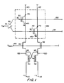
- Figure 1 is a schematic drawing of the circuit of one cell of an illustrative embodiment of the crossbar switch of this invention. Also shown are bias transistors and the pair of cross-coupled inverters this cell drives.
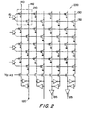
- FIG. 2 is a schematic diagram of a representative 4x4 subsection of an illustrative embodiment of a crossbar switch circuit constructed in accordance with the principles of this invention, showing the matrix layout of the cells.
- As shown in FIG. 1, a representative portion of a crossbar switch constructed in accordance with this invention includes
complementary wordlines complementary bitlines 140 and 142 viaprogrammable EPROM transistors EPROM transistors node 10 will not affect the output voltage, VOUT, atnode 120. However, ifEPROM transistors node 10, will be output at the appropriate output node, such as 120. Various EPROM transistors may be employed. For example,EPROM transistors - Referring to FIG. 1, the propagation of an input signal at
node 10 viaerased EPROM transistors output node 120 is described as follows, for both low to high and high to low transitions. Note the power supply voltage atnodes node 100 is in the range of 3.0 V, and the potential of theground nodes 150 is maintained in the range of 0 V. The bias transistor arrangement preventsnodes EPROM transistor - For a low to high transition, the initial state of
node 10 is low, thusEPROM transistor 50 is initially off, andnode 70 high. The high signal ofnode 70 is communicated via n-type buffer transistor 90 tonode 62, holding p-type transistor 42 off. The complement of thelow node 10 voltage atnode 52 holdsEPROM transistor 52 on, holdingnode 72 low. As p-type transistor 42 is off, only a negligible current flows in bit line 142. The low signal atnode 72 is communicated viabuffer transistor 92 tonode 60 where it holds p-type transistor 40 on. However, asEPROM transistor 50 is off, a negligible current flows inbit line 140. With no current flowing inbit lines 140 and 142, the standby power consumption of the circuit in FIG. 1 is near zero. Note the low signal atnode 72 is communicated tooutput node 120 viabuffer transistor 92. - A low to high transition at
input node 10 causesEPROM transistor 50 to turn on, pullingnode 70 low. This low voltage is transmitted tonode 62 viabuffer transistor 90, turning on p-type transistor 42.Low node 32, which is the complement ofhigh node 10, has turned offEPROM transistor 52. Thus, the turn-on of p-type transistor 42 bringsnode 60, and thereforeoutput node 120, high. Subsequently, p-type transistor 40 is turned off, blocking current flow inbit line 140. Since current flow is blocked in bit line 142 by turned offEPROM transistor 52, quiescent power dissipation is negligible as in the previous state, where the voltage VIN atnode 10 was low. - A high to low transition at
input node 10, takesnode 32 high, turningEPROM transistor 52 on, and forcingnode 72 low. This low voltage is transmitted via n-type buffer transistor 92 tonode 60 and theoutput node 120, turning p-type transistor 40 on. Sincenode 30 is low,EPROM transistor 50 is off. Thus, as p-type transistor 40 turns on, it bringsnode 62 high, turning off p-type transistor 42 and blocking current flow in bit line 142. Current flow is blocked inbit line 140 by turned offEPROM transistor 50. The cell has now been returned to its original state. - As shown in FIG. 2, the crossbar switch may also include
output buffers 215 to buffer and invert the output signal. Further, as shown in FIG. 1, it is also possible to provideoutput node 122, the complement ofnode 120. - From the above, it is apparent that not only does the circuit in FIG. 1 transmit input signals at
node 10 tooutput node 120, but that the circuit also provides for zero quiescent power consumption. - As the structure of two-
EPROM transistor cell 210 consumes less real estate on the chip, a higher level of integration is possible than if four EPROM transistors were committed to each cell. Twotransistor cell 210 also does not loadbit lines 140 and 142 andword lines - Although particular attention has been given to the operation of one cell of the crossbar switch circuit, it will be understood that the overall function of the chip is to programmably interconnect N inputs to N outputs, and that among other possible variations within the scope of the appended claims that will occur to those skilled in the art, any number of inputs and outputs may be used.
Claims (6)
- Integrated circuitry having a plurality of input terminals (VIN), a pair of wordline conductors associated with each of said input terminals (130, 132), a plurality of output terminals (120), a pair of bitline conductors associated with each of said output terminals (140, 142), circuitry (20) for applying true and complement versions of the signal applied to each input terminal to respective ones of the wordline conductors in the pair of wordline conductors associated with that input terminal, said pairs of wordline conductors intersecting said pairs of bitline conductors at a plurality of intersections,
characterized by:
at most a single pair of EPROM transistors (50, 52) at each intersection for programmably interconnecting each pair of wordline conductors (130, 132) to each pair of bitline conductors (140, 142). - The integrated circuitry defined in claim 1 wherein said EPROM transistors each have a gate and a source-drain channel, the gate of each EPROM transistor being connected to a respective one of the wordline conductors in the associated pair of wordline conductors (130, 132), and the source-drain channel of each EPROM transistor being connected to a respective one of the bitline conductors in the associated pair of bitline conductors (140, 142).
- The integrated circuitry defined in claim 2 wherein the source-drain channel of each EPROM transistor is connected in series between the bitline conductor to which that EPROM transistor is connected and a source of ground potential.
- The integrated circuitry defined in claim 3 further comprising a pair of p-channel transistors (40, 42) associated with each pair of bitline conductors, each of said p-channel transistors having a source-drain channel connected in series between one of said bitline conductors in said associated pair of bitline conductors and a source of logical 1 potential and having a gate which is connected to the other bitline conductor in said associated pair of bitline conductors.
- The integrated circuitry defined in claim 4 further comprising a pair of n-channel transistors (90, 92) associated with each pair of p-channel transistors, each of said n-channel transistors having a source-drain channel connected in series between one of said bitline conductors and the source-drain channel of the p-channel transistor associated with that bitline conductor, each n-channel transistor also having a gate connected to a source of bias potential which is intermediate said ground potential and said logical 1 potential.
- The integrated circuitry defined in claim 5 wherein the output terminal (120) associated with each pair of bitline conductors is connected between the p-channel and n-channel transistors whose source-drain channels are connected in series with one of the bitline conductors in that pair of bitline conductors.
Applications Claiming Priority (3)
| Application Number | Priority Date | Filing Date | Title |
|---|---|---|---|
| US81380291A | 1991-12-26 | 1991-12-26 | |
| US813802 | 1991-12-26 | ||
| PCT/US1992/011029 WO1993013629A1 (en) | 1991-12-26 | 1992-12-21 | Eprom-based crossbar switch with zero standby power |
Publications (3)
| Publication Number | Publication Date |
|---|---|
| EP0573637A1 EP0573637A1 (en) | 1993-12-15 |
| EP0573637A4 EP0573637A4 (en) | 1994-03-16 |
| EP0573637B1 true EP0573637B1 (en) | 1997-12-29 |
Family
ID=25213433
Family Applications (1)
| Application Number | Title | Priority Date | Filing Date |
|---|---|---|---|
| EP93901133A Expired - Lifetime EP0573637B1 (en) | 1991-12-26 | 1992-12-21 | Eprom-based crossbar switch with zero standby power |
Country Status (5)
| Country | Link |
|---|---|
| US (1) | US5517186A (en) |
| EP (1) | EP0573637B1 (en) |
| JP (1) | JPH06505848A (en) |
| DE (1) | DE69223772D1 (en) |
| WO (1) | WO1993013629A1 (en) |
Families Citing this family (13)
| Publication number | Priority date | Publication date | Assignee | Title |
|---|---|---|---|---|
| GB2300085A (en) * | 1995-04-18 | 1996-10-23 | Northern Telecom Ltd | A high speed switch |
| US6909659B2 (en) | 2001-08-30 | 2005-06-21 | Micron Technology, Inc. | Zero power chip standby mode |
| US6874136B2 (en) | 2002-01-10 | 2005-03-29 | M2000 | Crossbar device with reduced parasitic capacitive loading and usage of crossbar devices in reconfigurable circuits |
| US20050086040A1 (en) * | 2003-10-02 | 2005-04-21 | Curtis Davis | System incorporating physics processing unit |
| US7895411B2 (en) * | 2003-10-02 | 2011-02-22 | Nvidia Corporation | Physics processing unit |
| US7739479B2 (en) * | 2003-10-02 | 2010-06-15 | Nvidia Corporation | Method for providing physics simulation data |
| US20050251644A1 (en) * | 2004-05-06 | 2005-11-10 | Monier Maher | Physics processing unit instruction set architecture |
| US8255610B2 (en) | 2009-02-13 | 2012-08-28 | The Regents Of The University Of Michigan | Crossbar circuitry for applying a pre-selection prior to arbitration between transmission requests and method of operation of such crossbar circuitry |
| US9514074B2 (en) | 2009-02-13 | 2016-12-06 | The Regents Of The University Of Michigan | Single cycle arbitration within an interconnect |
| US8549207B2 (en) * | 2009-02-13 | 2013-10-01 | The Regents Of The University Of Michigan | Crossbar circuitry for applying an adaptive priority scheme and method of operation of such crossbar circuitry |
| US8230152B2 (en) * | 2009-02-13 | 2012-07-24 | The Regents Of The University Of Michigan | Crossbar circuitry and method of operation of such crossbar circuitry |
| US8000131B2 (en) * | 2009-04-29 | 2011-08-16 | Taiwan Semiconductor Manufacturing Company, Ltd | Non-volatile field programmable gate array |
| US8578384B2 (en) * | 2009-10-28 | 2013-11-05 | Freescale Semiconductor, Inc. | Method and apparatus for activating system components |
Family Cites Families (13)
| Publication number | Priority date | Publication date | Assignee | Title |
|---|---|---|---|---|
| US4317110A (en) * | 1980-06-30 | 1982-02-23 | Rca Corporation | Multi-mode circuit |
| DE3101932A1 (en) * | 1981-01-22 | 1982-09-02 | Licentia Patent-Verwaltungs-Gmbh, 6000 Frankfurt | "MATERIAL COUPLING FOR SIGNAL FREQUENCIES IN THE MEGAHERTZ RANGE" |
| US4433331A (en) * | 1981-12-14 | 1984-02-21 | Bell Telephone Laboratories, Incorporated | Programmable logic array interconnection matrix |
| US4644353A (en) * | 1985-06-17 | 1987-02-17 | Intersil, Inc. | Programmable interface |
| US4779010A (en) * | 1986-07-29 | 1988-10-18 | Advanced Micro Devices, Inc. | Monostable logic gate in a programmable logic array |
| LU86915A1 (en) * | 1986-10-07 | 1987-11-11 | Siemens Ag | BROADBAND SIGNAL DEVICE |
| JPS63108746A (en) * | 1986-10-27 | 1988-05-13 | Nec Corp | Programmable logic array |
| JPH01109921A (en) * | 1987-10-23 | 1989-04-26 | Ricoh Co Ltd | Programmable logic array |
| US4871930A (en) * | 1988-05-05 | 1989-10-03 | Altera Corporation | Programmable logic device with array blocks connected via programmable interconnect |
| LU87431A1 (en) * | 1988-06-08 | 1989-06-14 | Siemens Ag | BROADBAND SIGNAL DEVICE |
| US4899070A (en) * | 1988-07-13 | 1990-02-06 | Altera Corporation | Bit line sense amplifier for programmable logic devices |
| US5128565A (en) * | 1990-10-12 | 1992-07-07 | Altera Corporation | Sense amplifier with increased speed and reduced power consumption |
| US5220533A (en) * | 1991-11-06 | 1993-06-15 | Altera Corporation | Method and apparatus for preventing overerasure in a flash cell |
-
1992
- 1992-12-21 JP JP5511802A patent/JPH06505848A/en active Pending
- 1992-12-21 DE DE69223772T patent/DE69223772D1/en not_active Expired - Lifetime
- 1992-12-21 EP EP93901133A patent/EP0573637B1/en not_active Expired - Lifetime
- 1992-12-21 WO PCT/US1992/011029 patent/WO1993013629A1/en active IP Right Grant
-
1993
- 1993-11-30 US US08/159,189 patent/US5517186A/en not_active Expired - Fee Related
Also Published As
| Publication number | Publication date |
|---|---|
| EP0573637A1 (en) | 1993-12-15 |
| JPH06505848A (en) | 1994-06-30 |
| WO1993013629A1 (en) | 1993-07-08 |
| DE69223772D1 (en) | 1998-02-05 |
| EP0573637A4 (en) | 1994-03-16 |
| US5517186A (en) | 1996-05-14 |
Similar Documents
| Publication | Publication Date | Title |
|---|---|---|
| US5793681A (en) | Multiport memory cell circuit having read buffer for reducing read access time | |
| KR930006841B1 (en) | Ic memory circuit apparatus | |
| US4953127A (en) | Semiconductor memory having different read and write word line voltage levels | |
| US5706226A (en) | Low voltage CMOS SRAM | |
| KR100207941B1 (en) | Shared bicmos sense amplifier | |
| EP0573637B1 (en) | Eprom-based crossbar switch with zero standby power | |
| US5170373A (en) | Three transistor eeprom cell | |
| US5113374A (en) | Mos type semiconductor memory device having a word line resetting circuit | |
| US4899308A (en) | High density ROM in a CMOS gate array | |
| JP4717173B2 (en) | Memory device and method | |
| US5675548A (en) | Semiconductor integrated circuit having logi gates | |
| US7629812B2 (en) | Switching circuits and methods for programmable logic devices | |
| EP0136229B1 (en) | Sense amplifier | |
| US4866432A (en) | Field programmable matrix circuit for EEPROM logic cells | |
| US5570312A (en) | SRAM cell using word line controlled pull-up NMOS transistors | |
| EP0285015A2 (en) | Diode-FET logic circuitry | |
| US5831458A (en) | Output circuit having BiNMOS inverters | |
| JPH011328A (en) | electronic logic circuit | |
| US6314041B1 (en) | Memory with a reduced leakage current | |
| US4788460A (en) | Circuit arrangement of sense amplifier for rapid evaluation of logic state | |
| EP0256336B1 (en) | A programmable logic array | |
| US5305279A (en) | Semiconductor memory device having word line selection logic circuits | |
| KR100255542B1 (en) | Static semiconductor memory of flip-flop circuit type with driving n-channel transistor | |
| JPH09147564A (en) | Memory cell array | |
| KR100237118B1 (en) | Semiconductor memory with nand type memory cells |
Legal Events
| Date | Code | Title | Description |
|---|---|---|---|
| PUAI | Public reference made under article 153(3) epc to a published international application that has entered the european phase |
Free format text: ORIGINAL CODE: 0009012 |
|
| 17P | Request for examination filed |
Effective date: 19930908 |
|
| AK | Designated contracting states |
Kind code of ref document: A1 Designated state(s): BE DE DK ES FR GB GR IE IT LU NL PT |
|
| A4 | Supplementary search report drawn up and despatched |
Effective date: 19940126 |
|
| AK | Designated contracting states |
Kind code of ref document: A4 Designated state(s): BE DE DK ES FR GB GR IE IT LU NL PT |
|
| 17Q | First examination report despatched |
Effective date: 19960312 |
|
| GRAG | Despatch of communication of intention to grant |
Free format text: ORIGINAL CODE: EPIDOS AGRA |
|
| GRAG | Despatch of communication of intention to grant |
Free format text: ORIGINAL CODE: EPIDOS AGRA |
|
| GRAG | Despatch of communication of intention to grant |
Free format text: ORIGINAL CODE: EPIDOS AGRA |
|
| GRAH | Despatch of communication of intention to grant a patent |
Free format text: ORIGINAL CODE: EPIDOS IGRA |
|
| GRAH | Despatch of communication of intention to grant a patent |
Free format text: ORIGINAL CODE: EPIDOS IGRA |
|
| GRAA | (expected) grant |
Free format text: ORIGINAL CODE: 0009210 |
|
| AK | Designated contracting states |
Kind code of ref document: B1 Designated state(s): BE DE DK ES FR GB GR IE IT LU NL PT |
|
| PG25 | Lapsed in a contracting state [announced via postgrant information from national office to epo] |
Ref country code: NL Free format text: LAPSE BECAUSE OF FAILURE TO SUBMIT A TRANSLATION OF THE DESCRIPTION OR TO PAY THE FEE WITHIN THE PRESCRIBED TIME-LIMIT Effective date: 19971229 Ref country code: IT Free format text: LAPSE BECAUSE OF FAILURE TO SUBMIT A TRANSLATION OF THE DESCRIPTION OR TO PAY THE FEE WITHIN THE PRE;WARNING: LAPSES OF ITALIAN PATENTS WITH EFFECTIVE DATE BEFORE 2007 MAY HAVE OCCURRED AT ANY TIME BEFORE 2007. THE CORRECT EFFECTIVE DATE MAY BE DIFFERENT FROM THE ONE RECORDED.SCRIBED TIME-LIMIT Effective date: 19971229 Ref country code: IE Free format text: LAPSE BECAUSE OF NON-PAYMENT OF DUE FEES Effective date: 19971229 Ref country code: GR Free format text: LAPSE BECAUSE OF NON-PAYMENT OF DUE FEES Effective date: 19971229 Ref country code: FR Free format text: LAPSE BECAUSE OF FAILURE TO SUBMIT A TRANSLATION OF THE DESCRIPTION OR TO PAY THE FEE WITHIN THE PRESCRIBED TIME-LIMIT Effective date: 19971229 Ref country code: ES Free format text: THE PATENT HAS BEEN ANNULLED BY A DECISION OF A NATIONAL AUTHORITY Effective date: 19971229 Ref country code: DK Free format text: LAPSE BECAUSE OF NON-PAYMENT OF DUE FEES Effective date: 19971229 Ref country code: BE Free format text: LAPSE BECAUSE OF FAILURE TO SUBMIT A TRANSLATION OF THE DESCRIPTION OR TO PAY THE FEE WITHIN THE PRESCRIBED TIME-LIMIT Effective date: 19971229 |
|
| REF | Corresponds to: |
Ref document number: 69223772 Country of ref document: DE Date of ref document: 19980205 |
|
| RAP2 | Party data changed (patent owner data changed or rights of a patent transferred) |
Owner name: ALTERA CORPORATION (A DELAWARE CORPORATION) |
|
| PG25 | Lapsed in a contracting state [announced via postgrant information from national office to epo] |
Ref country code: PT Free format text: LAPSE BECAUSE OF FAILURE TO SUBMIT A TRANSLATION OF THE DESCRIPTION OR TO PAY THE FEE WITHIN THE PRESCRIBED TIME-LIMIT Effective date: 19980330 |
|
| PG25 | Lapsed in a contracting state [announced via postgrant information from national office to epo] |
Ref country code: DE Free format text: LAPSE BECAUSE OF FAILURE TO SUBMIT A TRANSLATION OF THE DESCRIPTION OR TO PAY THE FEE WITHIN THE PRESCRIBED TIME-LIMIT Effective date: 19980331 |
|
| NLT2 | Nl: modifications (of names), taken from the european patent patent bulletin |
Owner name: ALTERA CORPORATION (A DELAWARE CORPORATION) |
|
| EN | Fr: translation not filed | ||
| NLV1 | Nl: lapsed or annulled due to failure to fulfill the requirements of art. 29p and 29m of the patents act | ||
| REG | Reference to a national code |
Ref country code: IE Ref legal event code: FG4D Free format text: 78030 |
|
| PLBE | No opposition filed within time limit |
Free format text: ORIGINAL CODE: 0009261 |
|
| STAA | Information on the status of an ep patent application or granted ep patent |
Free format text: STATUS: NO OPPOSITION FILED WITHIN TIME LIMIT |
|
| PG25 | Lapsed in a contracting state [announced via postgrant information from national office to epo] |
Ref country code: LU Free format text: LAPSE BECAUSE OF NON-PAYMENT OF DUE FEES Effective date: 19981221 |
|
| 26N | No opposition filed | ||
| REG | Reference to a national code |
Ref country code: GB Ref legal event code: IF02 |
|
| PGFP | Annual fee paid to national office [announced via postgrant information from national office to epo] |
Ref country code: GB Payment date: 20051104 Year of fee payment: 14 |
|
| GBPC | Gb: european patent ceased through non-payment of renewal fee |
Effective date: 20061221 |
|
| PG25 | Lapsed in a contracting state [announced via postgrant information from national office to epo] |
Ref country code: GB Free format text: LAPSE BECAUSE OF NON-PAYMENT OF DUE FEES Effective date: 20061221 |