EP0572564B1 - Parity calculation in an efficient array of mass storage devices - Google Patents
Parity calculation in an efficient array of mass storage devices Download PDFInfo
- Publication number
- EP0572564B1 EP0572564B1 EP92908308A EP92908308A EP0572564B1 EP 0572564 B1 EP0572564 B1 EP 0572564B1 EP 92908308 A EP92908308 A EP 92908308A EP 92908308 A EP92908308 A EP 92908308A EP 0572564 B1 EP0572564 B1 EP 0572564B1
- Authority
- EP
- European Patent Office
- Prior art keywords
- hard disk
- parity
- disk drive
- data
- block
- Prior art date
- Legal status (The legal status is an assumption and is not a legal conclusion. Google has not performed a legal analysis and makes no representation as to the accuracy of the status listed.)
- Expired - Lifetime
Links
Images


Classifications
-
- G—PHYSICS
- G06—COMPUTING; CALCULATING OR COUNTING
- G06F—ELECTRIC DIGITAL DATA PROCESSING
- G06F11/00—Error detection; Error correction; Monitoring
- G06F11/07—Responding to the occurrence of a fault, e.g. fault tolerance
- G06F11/08—Error detection or correction by redundancy in data representation, e.g. by using checking codes
- G06F11/10—Adding special bits or symbols to the coded information, e.g. parity check, casting out 9's or 11's
- G06F11/1076—Parity data used in redundant arrays of independent storages, e.g. in RAID systems
-
- G—PHYSICS
- G11—INFORMATION STORAGE
- G11B—INFORMATION STORAGE BASED ON RELATIVE MOVEMENT BETWEEN RECORD CARRIER AND TRANSDUCER
- G11B20/00—Signal processing not specific to the method of recording or reproducing; Circuits therefor
- G11B20/10—Digital recording or reproducing
- G11B20/18—Error detection or correction; Testing, e.g. of drop-outs
- G11B20/1833—Error detection or correction; Testing, e.g. of drop-outs by adding special lists or symbols to the coded information
-
- G—PHYSICS
- G06—COMPUTING; CALCULATING OR COUNTING
- G06F—ELECTRIC DIGITAL DATA PROCESSING
- G06F2211/00—Indexing scheme relating to details of data-processing equipment not covered by groups G06F3/00 - G06F13/00
- G06F2211/10—Indexing scheme relating to G06F11/10
- G06F2211/1002—Indexing scheme relating to G06F11/1076
- G06F2211/1054—Parity-fast hardware, i.e. dedicated fast hardware for RAID systems with parity
Definitions
- This invention relates in general to data storage devices for computers, and more particularly to mass storage memory arrays.
- mirroring Another problem is that although top quality disk drives offer a mean time between failure of about 150,000 hours, in systems using multiple disk drives failures will occur.
- One approach to addressing the failure problem is called mirroring.
- the host computer writes data to two disk drives simultaneously. If one disk drive fails, a copy of all the data is immediately available on the other drive.
- Mirroring protects against a failure in one drive but it requires a user to purchase twice as much storage to hold the data and programs. Mirroring also does not address the I/O bottle-neck problem.
- a RAID system is a group of intelligent disk drives under the control of a single device driver or host computer.
- the proposed RAID system offers significantly higher performance than a single disk drive. Data can be striped or dispensed among several drives so that several of the drives are accessed in parallel to read one block of data which was striped across the several drives. This provides for quicker access than retrieving the block from a single drive.
- check bytes are stored, also preferably in an interleaved pattern across all of the drives.
- the check (or parity) byte is the sum of the data stored on the other drives in the same position. Therefore, if one drive fails the data which was stored on that drive can be quickly recreated by a calculation involving a check byte and data on the other non-failed drives for the same position. All of the above calculations are performed by the host computer.
- the host computer When the host is instructed to write a block of new data which may be designated "NA" to a disk drive, the host computer first reads the old data "A” from the position to which the new data "NA” will be stored and the corresponding check bytes or parity bytes "PA” as shown in Fig. 2. Incidentally, the old parity designated “PA” is the parity involving not only the data "A", but also data from other disk drives. The host then calculates the new check bytes NPA by subtracting out the old data "A” and summing in the new data "PA”. The check bytes are then rewritten over the old check bytes and the new data "NA” is written to the position where the old data "A" previously resided.
- the host processor is forced to do a large number of calculations and multiple transfers of data over the bus which connects the host and the disk drives each time a block of data is to be written to a disk drive.
- the large number of calculations and the bus transfers reduces the performance of the host computer and the overall system.
- the principal objects of the present invention are to reduce the involvement of the host computer in the data storage process and to minimize the number of data transfers along the bus which interconnects the disk drives and the host computer.
- US-A-4 761 785 discloses a so called RAID5 system teaching the use of a redundant array of hard disks, where parity data is spread over all of said plurality of hard disks.
- EP-0297507 discloses a memory back-up system deploying a number of primary memory units which are backed up by a single memory unit which holds the check sums of all data held in the primary memory units.
- EP-0297507 teaches generating a partial parity checksum by calculating the exclusive-OR of old data from a primary unit with new data, sending this partial parity checksum to the back-up memory unit and calculating the Exclusive OR of this partial parity checksum with the corresponding old check sum to be stored in the back-up unit, it does not interleave parity information over the memory units, calculates parity only on a word-by word basis and does not deploy hard disk drives suitable for the present invention.
- an efficient, redundant array of mass storage devices which includes a plurality of hard disk drives, a controller or processor associated with each hard disk drive, a host computer and at least one bus for communications between the host computer and the plurality of hard disk drives includes partial parity calculating means for calculating the Exclusive OR function of old data and new data, and parity calculating means for calculating the Exclusive Or of partial parity and old parity.
- Another aspect of the present invention encompasses a method for writing data to and calculating new parity data for a plurality of peripheral storage devices and a system which includes a host computer connected by a bus to a plurality of disk drives, each with its own controller.
- the system calculates the partial parity which is the Exclusive Or function of the old data and the new data which is to be stored in a location which currently holds the old data.
- the partial parity is calculated at the controller for the storage device to which the new data is written.
- the new data is written to the location in the peripheral storage device from which the old data was obtained.
- the partial parity data is then written to the controller of a peripheral storage device which contains the old parity data for the location to which the new data was written.
- the controller which receives the partial parity calculates the new parity which is the Exclusive Or function of the partial parity and the old parity.
- the new parity data is written to the location in the peripheral storage device which formerly held the old parity data.
- Fig. 1 shows a preferred embodiment of the present invention.
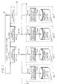
- the host computer 12 preferably a micro-computer based on the Extended Industry Standard Architecture (EISA) is shown with a plurality of interface adaptor cards 14 for coupling the host computer to a plurality of buses 16, preferably a Small Computer System Interface Bus or SCSI bus.
- the SCSI buses interconnect the host computer and a plurality of peripheral storage devices 18.
- Each peripheral storage device 18 preferably includes a dedicated spindle processor or controller 20 for each peripheral storage device, and a rotary disk drive 22 or other similar mass storage device.
- the rotary disk drives 22 are 51 ⁇ 4" Winchester hard disk drives.
- the peripheral storage devices 18 could be implemented using 1580 series or 1370 series disk drives manufactured by Micropolis of Chatsworth, California.
- Fig. 2 shows a prior art RAID system as was discussed in the BACKGROUND OF THE INVENTION section of this specification.
- the host computer 12 is shown with more detail including the host computer's host (central) processor 24 and its dynamic memory 26.
- the dynamic memory 26 is shown containing a block of data A and an identical size block of new data NA.
- Data block A was retrieved from the buffer memory 32 from peripheral storage device 18a. Data A had originated in the disk drive 22. Data A was then transferred to buffer memory 32 and then to the host computer's dynamic memory 26.
- parity data PA As can also be seen in Fig. 3, within peripheral storage device 18b the parity data (check bytes) PA has been written from disk drive 22 to buffer memory 32.
- the parity data PA provides a parity check for all the data stored in all of the disk drives in the system in the same location as data block A.
- the parity data is discussed in more detail below.
- the host processor 24 then generates partial parity data (PPA) which is the Exclusive Or of data A and data NA.
- PPA partial parity data
- Data NA is then written to the buffer storage of peripheral memory device 18a and from there data NA is written to the same location formerly occupied by the old data A in disk drive 22 within peripheral memory device 18a.
- the partial parity PPA is written to buffer memory 32 of peripheral memory device 18b.
- Disk drive processor 34 within peripheral memory device 18b then calculates the new parity data NPA which is the Exclusive OR of PPA and PA.
- the new parity data NPA is then written to the same location from which PA was retrieved in disk drive 22 within peripheral memory device 18b.
- the above described configuration approach allows the disk drive processor of the peripheral storage device containing the old priority data PA to calculate the new priority data NPA by performing the Exclusive Or of PPA and PA. This saves the host computer from having to perform that function. Also, the SCSI bus has one less data transfer along it. The data PA is never transferred along the bus. Therefore less bus time is also utilized which frees up the SCSI bus for data retrieval.
- FIG. 5 shows the dynamic memory 26 of the host computer 12 containing the new data NA to be written to one of the peripheral storage devices.
- Peripheral storage device 18a is shown with the old data A in its buffer memory 32.
- the new data NA is also shown as having been written to the buffer memory 32 of peripheral 18a.
- the buffer memory 32 of peripheral device 18b contains the old parity data PA.
- the disk drive processor 34 of peripheral 18a calculates the partial parity data PPA which is the Exclusive Or of A and NA.
- Fig. 6 shows PPA stored in buffer memory 32 of peripheral 18a after the calculation.
- PPA is then written to the buffer memory 32 of peripheral 18b.
- NA is also written to the location which held A in the disk drive 22.
- the disk drive processor 35 of peripheral 18b then calculates NPA (the new parity data) which is the Exclusive Or of PPA and PA. NA is then written to the location on disk drive 22 which previously contained PA.
- two disk drive processors calculated NPA and PPA. This saves the host computer from having to perform both of those calculations. Also, as in the previously described embodiment, the SCSI bus has one less data transfer along it as compared with the prior art systems. Therefore, less bus time is utilized, which frees up the SCSI bus for other functions.
- the parity data allows the system to recreate the data stored on one disk drive from the data stored on the other drives.
- the parity data is the Exclusive Or of the data stored in the same location on each drive.
- the parity data would operate as follows. If location A on drive 1 contained the value 7 and location A on drive 2 contained the value 3 then the parity data stored in location A on drive 3 would be the Exclusive Or of 7 and 3.
- 0111 In a four bit system 7 is represented as 0111 and three is represented as 0011.
- the Exclusive Or of 0111 and 0011 is 0100. If drive 1 fails, the data that was stored in location A of drive 1 is the Exclusive OR of the parity data for location A, 0100 (which is stored in location A on drive 3) and the data stored in location A on drive 2, 0011.
- the Exclusive Or of 0100 and 0011 is 0111 or 7. This approach works for any number of drives.
- Fig. 7 is a pictorial representation of the interleaving of data and parity information across four peripheral storage devices.
- Pie shaped sections 1, 2 and 3 represent identical locations on three different drives with P(1-2-3) representing the parity data which is stored in the same position as Sections 1, 2 and 3 on the fourth drive.
- P(1-2-3) representing the parity data which is stored in the same position as Sections 1, 2 and 3 on the fourth drive.
- the parity data for locations 5, 6 and 4 is shown stored on the third drive in sequence.
- Interleaving of the data can greatly increase the access speed of the overall peripheral memory storage system.
- each drive When a data block is accessed, each drive can simultaneously access its portion of the requested data and transmit it in parallel to the host.
Abstract
Description
Claims (15)
- A method for writing data blocks to and calculating new parity data blocks for an efficient, redundant array of hard disk devices (18) in a system which includes a host computer (12) connected via a bus (16) to a plurality of hard disk drives (22), each with its own hard disk drive controller (34) and memory (32), comprising the steps of:calculating a partial parity block (PPA) which is the Exclusive OR function of the old data block (A) and the new data block (NA) which is to be stored in the location which holds the old data block (A);writing the new data block (NA) to the location in the hard disk device (18) from which the old data block was obtained;transferring the calculated partial parity block (PPA) to the corresponding one of said plurality of hard disk drive controllers (32) of the hard disk device (18) which contains the old parity data block (A) for the location to which the new data block was written;calculating the new parity block (NPA) which is the Exclusive OR function of the partial parity block (PPA) and the old parity block (PA) at the hard disk drive controller (34) which receives the partial parity block;transferring the new parity block to the location in the hard disk device (18) which formerly held the old parity block; andinterleaving data blocks and parity blocks across all of the said plurality of hard disk devices (18).
- The method as described in Claim 1 wherein the partial parity (PPA) block is calculated by a first hard disk drive controller (34) which is the hard disk drive controller (34) of the hard disk device (18) to which the new data is being written.
- The method as described in Claim 1 wherein the host computer (12) calculates the partial parity (PPA).
- The method as described in Claim 2 further including the steps of:the first hard disk drive controller (34) receiving the new data (NA) from the host computer (24); andthe first hard disk drive controller (34) obtaining the old data (A) from its associated hard disk drive (22).
- The method as described in Claim 4 wherein said first hard disk drive controller (34) performs the step of transferring the partial parity (PPA) to the hard disk drive controller (34) of a hard disk device (18) which contains the old parity data (PA) for the location to which the new data was written.
- The method as described in Claim 1, wherein said hard disk drives (22) are 5¼" disk drives.
- The method as in Claim 1, wherein said bus (16) is a Small Computer System Interface bus.
- A computer system adapted to write data blocks to, and calculate new parity data blocks for, an efficient, redundant array of hard disk devices (18), said system comprising:a host computer (12) ;a plurality of hard disk drives (22) each with its own hard disk drive (34) controller and memory (32);a bus (16) interconnecting said hard disk drives (22) and said host computer (12);means for calculating a partial parity block (PPA) which is the Exclusive OR function of the old data block (A) and the new data block (NA) which is to be stored in the location which holds the old data block (A);means for writing the new data block (NA) to the location in the hard disk device (18) from which the old data block was obtained;means for transferring the calculated partial parity block (PPA) to the corresponding one of said plurality of hard disk drive controllers (32) of a hard disk device (18) which contains the old parity data block (A) for the location to which the new data block was written;means for calculating the new parity block (NPA) which is the Exclusive OR function of the partial parity block (PPA) and the old parity block (PA) at the hard disk drive controller (34) which receives the partial parity block;means for transferring the new parity block to the location in the hard disk device which formerly held the old parity block; andmeans for interleaving data blocks and parity blocks across all of the said plurality of hard disk drives.
- A computer system as defined in Claim 8 wherein each of the said hard disk drive controllers (34) includes said means for calculating partial parity data blocks by calculating the Exclusive OR function of old data blocks and new data blocks.
- A computer system as defined in Claim 9 wherein said hard disk drive controller (34) further includes means for receiving new data blocks from said host computer (12) and retrieving old data blocks from the hard disk drive (34) associated with said hard disk drive controller (34).
- A computer system as defined in Claim 10 wherein said hard disk drive controller (34) further includes means for transferring said partial parity data blocks to a second hard disk drive controller (34).
- A computer system as defined in Claim 10 wherein said hard disk drive controller (34) further includes means for storing the new parity data blocks on the disk drive associated with that hard disk drive controller (34) and in the same location as the old parity data blocks previously resided.
- A computer system as defined in Claim 10 wherein said hard disk drive controller (34) further includes means for storing the new data blocks in the same location as the old data blocks previously resided on the disk drive associated with the hard disk drive controller (34).
- A computer system as defined in Claim 8 wherein said hard disk drives (22) are 5¼" Winchester drives.
- A computer system as defined in Claim 12 wherein said bus (16) is a Small Computer System Interface bus.
Applications Claiming Priority (3)
| Application Number | Priority Date | Filing Date | Title |
|---|---|---|---|
| US07/658,317 US5191584A (en) | 1991-02-20 | 1991-02-20 | Mass storage array with efficient parity calculation |
| US658317 | 1991-02-20 | ||
| PCT/US1992/001257 WO1992015057A1 (en) | 1991-02-20 | 1992-02-18 | Parity calculation in an efficient array of mass storage devices |
Publications (3)
| Publication Number | Publication Date |
|---|---|
| EP0572564A1 EP0572564A1 (en) | 1993-12-08 |
| EP0572564A4 EP0572564A4 (en) | 1994-02-16 |
| EP0572564B1 true EP0572564B1 (en) | 1998-12-16 |
Family
ID=24640749
Family Applications (1)
| Application Number | Title | Priority Date | Filing Date |
|---|---|---|---|
| EP92908308A Expired - Lifetime EP0572564B1 (en) | 1991-02-20 | 1992-02-18 | Parity calculation in an efficient array of mass storage devices |
Country Status (5)
| Country | Link |
|---|---|
| US (1) | US5191584A (en) |
| EP (1) | EP0572564B1 (en) |
| CA (1) | CA2098988C (en) |
| DE (1) | DE69227896T2 (en) |
| WO (1) | WO1992015057A1 (en) |
Families Citing this family (121)
| Publication number | Priority date | Publication date | Assignee | Title |
|---|---|---|---|---|
| JPH04184634A (en) * | 1990-11-20 | 1992-07-01 | Matsushita Electric Ind Co Ltd | Microcomputer |
| DE69132618T2 (en) * | 1990-11-09 | 2001-09-13 | Seagate Technology Llc | CONTROL ARCHITECTURE FOR HARD DISK DRIVE WITH SEVERAL MICROCONTROLLERS |
| JP2913917B2 (en) * | 1991-08-20 | 1999-06-28 | 株式会社日立製作所 | Storage device and storage device system |
| US5522065A (en) * | 1991-08-30 | 1996-05-28 | Compaq Computer Corporation | Method for performing write operations in a parity fault tolerant disk array |
| US5506977A (en) * | 1991-12-17 | 1996-04-09 | Dell Usa, L.P. | Method and controller for minimizing reads during partial stripe write operations to a disk drive |
| US5287462A (en) * | 1991-12-20 | 1994-02-15 | Ncr Corporation | Bufferless SCSI to SCSI data transfer scheme for disk array applications |
| US5337322A (en) * | 1992-03-02 | 1994-08-09 | Acer Incorporated | Method of processing stored data containing parity data |
| US5398253A (en) * | 1992-03-11 | 1995-03-14 | Emc Corporation | Storage unit generation of redundancy information in a redundant storage array system |
| US5724539A (en) * | 1992-03-19 | 1998-03-03 | Digital Equipment Corporation | System for selectively storing stripes of data in tracks of disks so that sum of transfer rates of stripes match communication bandwidth to host |
| EP0654159A4 (en) * | 1992-08-10 | 1998-06-03 | Advanced Logic Res Inc | Computer interface for concurrently performing plural seeks on plural disk drives. |
| DE4309148A1 (en) * | 1993-03-22 | 1994-09-29 | Siemens Nixdorf Inf Syst | Disk array with load balancing |
| US5617425A (en) * | 1993-05-26 | 1997-04-01 | Seagate Technology, Inc. | Disc array having array supporting controllers and interface |
| JP3264465B2 (en) * | 1993-06-30 | 2002-03-11 | 株式会社日立製作所 | Storage system |
| US5530948A (en) * | 1993-12-30 | 1996-06-25 | International Business Machines Corporation | System and method for command queuing on raid levels 4 and 5 parity drives |
| CA2134016A1 (en) * | 1994-01-07 | 1995-07-08 | Peter B. Bandy | Data storage device and method of operation |
| WO1995026103A1 (en) * | 1994-03-18 | 1995-09-28 | Micropolis Corporation | On-demand video server system |
| JPH07281840A (en) * | 1994-04-14 | 1995-10-27 | Ibm Japan Ltd | Dual-disk recording device |
| US5519435A (en) * | 1994-09-01 | 1996-05-21 | Micropolis Corporation | Multi-user, on-demand video storage and retrieval system including video signature computation for preventing excessive instantaneous server data rate |
| JP3661205B2 (en) * | 1994-09-09 | 2005-06-15 | 株式会社日立製作所 | Disk array system and method for generating parity data of disk array system |
| US5412668A (en) * | 1994-09-22 | 1995-05-02 | International Business Machines Corporation | Parity striping feature for optical disks |
| US5634033A (en) * | 1994-12-16 | 1997-05-27 | At&T Global Information Solutions Company | Disk array storage system architecture for parity operations simultaneous with other data operations |
| US5745671A (en) * | 1995-02-28 | 1998-04-28 | International Business Machines Corporation | Data storage system with localized XOR function |
| US5630054A (en) * | 1995-04-18 | 1997-05-13 | Mti Technology Center | Method and apparatus for storing and retrieving error check information |
| US5862312A (en) * | 1995-10-24 | 1999-01-19 | Seachange Technology, Inc. | Loosely coupled mass storage computer cluster |
| US6484269B1 (en) * | 1995-11-09 | 2002-11-19 | Emc Corporation | Data storage system and method with improved data integrity value calculation |
| US5742752A (en) * | 1995-12-29 | 1998-04-21 | Symbios Logic Inc. | Method for performing a RAID stripe write operation using a drive XOR command set |
| EP0788051B1 (en) * | 1996-01-31 | 2002-05-15 | Kabushiki Kaisha Toshiba | I/O control method having recovery function |
| US6161165A (en) * | 1996-11-14 | 2000-12-12 | Emc Corporation | High performance data path with XOR on the fly |
| JP3133004B2 (en) | 1996-11-21 | 2001-02-05 | 株式会社日立製作所 | Disk array device and control method therefor |
| US5946707A (en) * | 1997-02-28 | 1999-08-31 | Adaptec, Inc. | Interleaved burst XOR using a single memory pointer |
| US5968182A (en) * | 1997-05-12 | 1999-10-19 | International Business Machines Corporation | Method and means for utilizing device long busy response for resolving detected anomalies at the lowest level in a hierarchical, demand/response storage management subsystem |
| US6151641A (en) * | 1997-09-30 | 2000-11-21 | Lsi Logic Corporation | DMA controller of a RAID storage controller with integrated XOR parity computation capability adapted to compute parity in parallel with the transfer of data segments |
| JP2001519563A (en) | 1997-10-08 | 2001-10-23 | シーゲイト テクノロジー エルエルシー | Disk drive array and data storage method |
| US6430701B1 (en) | 1998-01-27 | 2002-08-06 | Aiwa Co., Ltd. | Data recording and reproducing method and apparatus using plurality of data recording and reproducing units, and computer-readable recording medium |
| US6343343B1 (en) | 1998-07-31 | 2002-01-29 | International Business Machines Corporation | Disk arrays using non-standard sector sizes |
| US6986097B1 (en) * | 2002-02-21 | 2006-01-10 | Ciena Corporation | Method and apparatus for generating parity bits in a forward error correction (FEC) system |
| US6971042B2 (en) * | 2002-04-18 | 2005-11-29 | Huge Systems, Inc. | Media server with single chip storage controller |
| US6950894B2 (en) * | 2002-08-28 | 2005-09-27 | Intel Corporation | Techniques using integrated circuit chip capable of being coupled to storage system |
| US20040059954A1 (en) * | 2002-09-20 | 2004-03-25 | Rainer Hoehler | Automatic low power state entry |
| US7130229B2 (en) * | 2002-11-08 | 2006-10-31 | Intel Corporation | Interleaved mirrored memory systems |
| US7017017B2 (en) | 2002-11-08 | 2006-03-21 | Intel Corporation | Memory controllers with interleaved mirrored memory modes |
| US6944733B2 (en) * | 2002-12-11 | 2005-09-13 | Intel Corporation | Data storage using wireless communication |
| US7418646B2 (en) * | 2004-03-02 | 2008-08-26 | Intel Corporation | Integrated circuit using wireless communication to store and/or retrieve data and/or check data |
| US7496785B2 (en) * | 2006-03-21 | 2009-02-24 | International Business Machines Corporation | Enclosure-based raid parity assist |
| WO2007132457A2 (en) | 2006-05-12 | 2007-11-22 | Anobit Technologies Ltd. | Combined distortion estimation and error correction coding for memory devices |
| WO2007132452A2 (en) | 2006-05-12 | 2007-11-22 | Anobit Technologies | Reducing programming error in memory devices |
| WO2007132456A2 (en) | 2006-05-12 | 2007-11-22 | Anobit Technologies Ltd. | Memory device with adaptive capacity |
| WO2007132453A2 (en) | 2006-05-12 | 2007-11-22 | Anobit Technologies Ltd. | Distortion estimation and cancellation in memory devices |
| US8060806B2 (en) * | 2006-08-27 | 2011-11-15 | Anobit Technologies Ltd. | Estimation of non-linear distortion in memory devices |
| CN101601094B (en) * | 2006-10-30 | 2013-03-27 | 苹果公司 | Reading memory cells using multiple thresholds |
| WO2008053472A2 (en) * | 2006-10-30 | 2008-05-08 | Anobit Technologies Ltd. | Reading memory cells using multiple thresholds |
| US7924648B2 (en) * | 2006-11-28 | 2011-04-12 | Anobit Technologies Ltd. | Memory power and performance management |
| US7706182B2 (en) * | 2006-12-03 | 2010-04-27 | Anobit Technologies Ltd. | Adaptive programming of analog memory cells using statistical characteristics |
| US8151163B2 (en) | 2006-12-03 | 2012-04-03 | Anobit Technologies Ltd. | Automatic defect management in memory devices |
| US7900102B2 (en) | 2006-12-17 | 2011-03-01 | Anobit Technologies Ltd. | High-speed programming of memory devices |
| US7751240B2 (en) * | 2007-01-24 | 2010-07-06 | Anobit Technologies Ltd. | Memory device with negative thresholds |
| US8151166B2 (en) | 2007-01-24 | 2012-04-03 | Anobit Technologies Ltd. | Reduction of back pattern dependency effects in memory devices |
| US8369141B2 (en) * | 2007-03-12 | 2013-02-05 | Apple Inc. | Adaptive estimation of memory cell read thresholds |
| US8001320B2 (en) | 2007-04-22 | 2011-08-16 | Anobit Technologies Ltd. | Command interface for memory devices |
| US8234545B2 (en) | 2007-05-12 | 2012-07-31 | Apple Inc. | Data storage with incremental redundancy |
| US8429493B2 (en) | 2007-05-12 | 2013-04-23 | Apple Inc. | Memory device with internal signap processing unit |
| US7925936B1 (en) | 2007-07-13 | 2011-04-12 | Anobit Technologies Ltd. | Memory device with non-uniform programming levels |
| US8259497B2 (en) * | 2007-08-06 | 2012-09-04 | Apple Inc. | Programming schemes for multi-level analog memory cells |
| US8174905B2 (en) * | 2007-09-19 | 2012-05-08 | Anobit Technologies Ltd. | Programming orders for reducing distortion in arrays of multi-level analog memory cells |
| US7773413B2 (en) * | 2007-10-08 | 2010-08-10 | Anobit Technologies Ltd. | Reliable data storage in analog memory cells in the presence of temperature variations |
| US8000141B1 (en) | 2007-10-19 | 2011-08-16 | Anobit Technologies Ltd. | Compensation for voltage drifts in analog memory cells |
| US8068360B2 (en) | 2007-10-19 | 2011-11-29 | Anobit Technologies Ltd. | Reading analog memory cells using built-in multi-threshold commands |
| US8527819B2 (en) * | 2007-10-19 | 2013-09-03 | Apple Inc. | Data storage in analog memory cell arrays having erase failures |
| KR101509836B1 (en) * | 2007-11-13 | 2015-04-06 | 애플 인크. | Optimized selection of memory units in multi-unit memory devices |
| US8225181B2 (en) * | 2007-11-30 | 2012-07-17 | Apple Inc. | Efficient re-read operations from memory devices |
| US8209588B2 (en) | 2007-12-12 | 2012-06-26 | Anobit Technologies Ltd. | Efficient interference cancellation in analog memory cell arrays |
| US8456905B2 (en) * | 2007-12-16 | 2013-06-04 | Apple Inc. | Efficient data storage in multi-plane memory devices |
| US8085586B2 (en) * | 2007-12-27 | 2011-12-27 | Anobit Technologies Ltd. | Wear level estimation in analog memory cells |
| US8156398B2 (en) | 2008-02-05 | 2012-04-10 | Anobit Technologies Ltd. | Parameter estimation based on error correction code parity check equations |
| US7924587B2 (en) | 2008-02-21 | 2011-04-12 | Anobit Technologies Ltd. | Programming of analog memory cells using a single programming pulse per state transition |
| US7864573B2 (en) * | 2008-02-24 | 2011-01-04 | Anobit Technologies Ltd. | Programming analog memory cells for reduced variance after retention |
| US8230300B2 (en) | 2008-03-07 | 2012-07-24 | Apple Inc. | Efficient readout from analog memory cells using data compression |
| US8059457B2 (en) | 2008-03-18 | 2011-11-15 | Anobit Technologies Ltd. | Memory device with multiple-accuracy read commands |
| US8400858B2 (en) | 2008-03-18 | 2013-03-19 | Apple Inc. | Memory device with reduced sense time readout |
| US7924613B1 (en) * | 2008-08-05 | 2011-04-12 | Anobit Technologies Ltd. | Data storage in analog memory cells with protection against programming interruption |
| US7995388B1 (en) | 2008-08-05 | 2011-08-09 | Anobit Technologies Ltd. | Data storage using modified voltages |
| US8949684B1 (en) | 2008-09-02 | 2015-02-03 | Apple Inc. | Segmented data storage |
| US8169825B1 (en) | 2008-09-02 | 2012-05-01 | Anobit Technologies Ltd. | Reliable data storage in analog memory cells subjected to long retention periods |
| US8482978B1 (en) | 2008-09-14 | 2013-07-09 | Apple Inc. | Estimation of memory cell read thresholds by sampling inside programming level distribution intervals |
| US8000135B1 (en) | 2008-09-14 | 2011-08-16 | Anobit Technologies Ltd. | Estimation of memory cell read thresholds by sampling inside programming level distribution intervals |
| US8239734B1 (en) | 2008-10-15 | 2012-08-07 | Apple Inc. | Efficient data storage in storage device arrays |
| US8713330B1 (en) | 2008-10-30 | 2014-04-29 | Apple Inc. | Data scrambling in memory devices |
| US8208304B2 (en) * | 2008-11-16 | 2012-06-26 | Anobit Technologies Ltd. | Storage at M bits/cell density in N bits/cell analog memory cell devices, M>N |
| US8248831B2 (en) * | 2008-12-31 | 2012-08-21 | Apple Inc. | Rejuvenation of analog memory cells |
| US8397131B1 (en) | 2008-12-31 | 2013-03-12 | Apple Inc. | Efficient readout schemes for analog memory cell devices |
| US8924661B1 (en) | 2009-01-18 | 2014-12-30 | Apple Inc. | Memory system including a controller and processors associated with memory devices |
| US8228701B2 (en) | 2009-03-01 | 2012-07-24 | Apple Inc. | Selective activation of programming schemes in analog memory cell arrays |
| US8259506B1 (en) | 2009-03-25 | 2012-09-04 | Apple Inc. | Database of memory read thresholds |
| US8832354B2 (en) | 2009-03-25 | 2014-09-09 | Apple Inc. | Use of host system resources by memory controller |
| US8238157B1 (en) | 2009-04-12 | 2012-08-07 | Apple Inc. | Selective re-programming of analog memory cells |
| WO2010137178A1 (en) | 2009-05-25 | 2010-12-02 | Hitachi,Ltd. | Storage subsystem |
| US8479080B1 (en) | 2009-07-12 | 2013-07-02 | Apple Inc. | Adaptive over-provisioning in memory systems |
| US8495465B1 (en) | 2009-10-15 | 2013-07-23 | Apple Inc. | Error correction coding over multiple memory pages |
| US8458515B1 (en) * | 2009-11-16 | 2013-06-04 | Symantec Corporation | Raid5 recovery in a high availability object based file system |
| US8677054B1 (en) | 2009-12-16 | 2014-03-18 | Apple Inc. | Memory management schemes for non-volatile memory devices |
| US8694814B1 (en) | 2010-01-10 | 2014-04-08 | Apple Inc. | Reuse of host hibernation storage space by memory controller |
| US8677203B1 (en) | 2010-01-11 | 2014-03-18 | Apple Inc. | Redundant data storage schemes for multi-die memory systems |
| GB201003407D0 (en) * | 2010-03-01 | 2010-04-14 | Extas Global Ltd | Distributed storage and communication |
| US8694853B1 (en) | 2010-05-04 | 2014-04-08 | Apple Inc. | Read commands for reading interfering memory cells |
| US8572423B1 (en) | 2010-06-22 | 2013-10-29 | Apple Inc. | Reducing peak current in memory systems |
| US8595591B1 (en) | 2010-07-11 | 2013-11-26 | Apple Inc. | Interference-aware assignment of programming levels in analog memory cells |
| US9104580B1 (en) | 2010-07-27 | 2015-08-11 | Apple Inc. | Cache memory for hybrid disk drives |
| US8767459B1 (en) | 2010-07-31 | 2014-07-01 | Apple Inc. | Data storage in analog memory cells across word lines using a non-integer number of bits per cell |
| US8856475B1 (en) | 2010-08-01 | 2014-10-07 | Apple Inc. | Efficient selection of memory blocks for compaction |
| US8493781B1 (en) | 2010-08-12 | 2013-07-23 | Apple Inc. | Interference mitigation using individual word line erasure operations |
| US8694854B1 (en) | 2010-08-17 | 2014-04-08 | Apple Inc. | Read threshold setting based on soft readout statistics |
| US9021181B1 (en) | 2010-09-27 | 2015-04-28 | Apple Inc. | Memory management for unifying memory cell conditions by using maximum time intervals |
| EP2831735A1 (en) | 2012-04-27 | 2015-02-04 | Hitachi, Ltd. | Storage system and storage apparatus |
| CN104205059B (en) | 2012-04-27 | 2017-07-14 | 株式会社日立制作所 | Storage system and memory control device |
| US20150113204A1 (en) * | 2013-10-17 | 2015-04-23 | National Chiao Tung University | Data storage device and computing system with the same |
| JP6807457B2 (en) * | 2017-06-15 | 2021-01-06 | 株式会社日立製作所 | Storage system and storage system control method |
| US20190034306A1 (en) * | 2017-07-31 | 2019-01-31 | Intel Corporation | Computer System, Computer System Host, First Storage Device, Second Storage Device, Controllers, Methods, Apparatuses and Computer Programs |
| CN112074908A (en) | 2018-03-16 | 2020-12-11 | 美光科技公司 | NAND data placement mode |
| CN112074816A (en) * | 2018-03-16 | 2020-12-11 | 美光科技公司 | Cluster parity for NAND data placement mode |
| US11556416B2 (en) | 2021-05-05 | 2023-01-17 | Apple Inc. | Controlling memory readout reliability and throughput by adjusting distance between read thresholds |
| US11847342B2 (en) | 2021-07-28 | 2023-12-19 | Apple Inc. | Efficient transfer of hard data and confidence levels in reading a nonvolatile memory |
Family Cites Families (8)
| Publication number | Priority date | Publication date | Assignee | Title |
|---|---|---|---|---|
| US3789204A (en) * | 1972-06-06 | 1974-01-29 | Honeywell Inf Systems | Self-checking digital storage system |
| US3887901A (en) * | 1974-04-29 | 1975-06-03 | Sperry Rand Corp | Longitudinal parity generator for mainframe memories |
| US4016409A (en) * | 1976-03-01 | 1977-04-05 | Burroughs Corporation | Longitudinal parity generator for use with a memory |
| US4433388A (en) * | 1980-10-06 | 1984-02-21 | Ncr Corporation | Longitudinal parity |
| US4849978A (en) * | 1987-07-02 | 1989-07-18 | International Business Machines Corporation | Memory unit backup using checksum |
| US4870643A (en) * | 1987-11-06 | 1989-09-26 | Micropolis Corporation | Parallel drive array storage system |
| US5007053A (en) * | 1988-11-30 | 1991-04-09 | International Business Machines Corporation | Method and apparatus for checksum address generation in a fail-safe modular memory |
| US5088081A (en) * | 1990-03-28 | 1992-02-11 | Prime Computer, Inc. | Method and apparatus for improved disk access |
-
1991
- 1991-02-20 US US07/658,317 patent/US5191584A/en not_active Expired - Lifetime
-
1992
- 1992-02-18 DE DE69227896T patent/DE69227896T2/en not_active Expired - Lifetime
- 1992-02-18 WO PCT/US1992/001257 patent/WO1992015057A1/en active IP Right Grant
- 1992-02-18 EP EP92908308A patent/EP0572564B1/en not_active Expired - Lifetime
- 1992-02-18 CA CA002098988A patent/CA2098988C/en not_active Expired - Lifetime
Also Published As
| Publication number | Publication date |
|---|---|
| WO1992015057A1 (en) | 1992-09-03 |
| EP0572564A4 (en) | 1994-02-16 |
| CA2098988A1 (en) | 1992-08-21 |
| DE69227896T2 (en) | 1999-06-02 |
| CA2098988C (en) | 2003-02-11 |
| EP0572564A1 (en) | 1993-12-08 |
| DE69227896D1 (en) | 1999-01-28 |
| US5191584A (en) | 1993-03-02 |
Similar Documents
| Publication | Publication Date | Title |
|---|---|---|
| EP0572564B1 (en) | Parity calculation in an efficient array of mass storage devices | |
| US5487160A (en) | Concurrent image backup for disk storage system | |
| US5418925A (en) | Fast write I/O handling in a disk array using spare drive for buffering | |
| US6101615A (en) | Method and apparatus for improving sequential writes to RAID-6 devices | |
| US5526507A (en) | Computer memory array control for accessing different memory banks simullaneously | |
| US6009481A (en) | Mass storage system using internal system-level mirroring | |
| JP2769443B2 (en) | Storage subsystem and related apparatus / method | |
| EP0485110B1 (en) | Logical partitioning of a redundant array storage system | |
| US5720027A (en) | Redundant disc computer having targeted data broadcast | |
| KR100211788B1 (en) | Failure prediction for disk arrays | |
| US5596708A (en) | Method and apparatus for the protection of write data in a disk array | |
| EP0294287B1 (en) | Fault-tolerant, error-correcting storage system and method for storing digital information in such a storage system | |
| US5742752A (en) | Method for performing a RAID stripe write operation using a drive XOR command set | |
| US5959860A (en) | Method and apparatus for operating an array of storage devices | |
| US7228381B2 (en) | Storage system using fast storage device for storing redundant data | |
| EP0594464A2 (en) | Method of operating a data storage disk array | |
| CA2029151A1 (en) | Data redundancy and recovery protection | |
| EP0986000B1 (en) | Disk array subsystem | |
| JPH10105344A (en) | Data recorder system and data write method therefor | |
| US5805787A (en) | Disk based disk cache interfacing system and method | |
| US5787463A (en) | Disk array system including a dual-ported staging memory and concurrent redundancy calculation capability | |
| US5574736A (en) | Data storage device and method of operation | |
| JP2857288B2 (en) | Disk array device | |
| WO1992004674A1 (en) | Computer memory array control | |
| US6249842B1 (en) | Apparatus and method for processing data in a RAID system |
Legal Events
| Date | Code | Title | Description |
|---|---|---|---|
| PUAI | Public reference made under article 153(3) epc to a published international application that has entered the european phase |
Free format text: ORIGINAL CODE: 0009012 |
|
| 17P | Request for examination filed |
Effective date: 19930625 |
|
| AK | Designated contracting states |
Kind code of ref document: A1 Designated state(s): DE FR GB IT |
|
| A4 | Supplementary search report drawn up and despatched |
Effective date: 19931229 |
|
| AK | Designated contracting states |
Kind code of ref document: A4 Designated state(s): DE FR GB IT |
|
| 17Q | First examination report despatched |
Effective date: 19951206 |
|
| GRAG | Despatch of communication of intention to grant |
Free format text: ORIGINAL CODE: EPIDOS AGRA |
|
| GRAG | Despatch of communication of intention to grant |
Free format text: ORIGINAL CODE: EPIDOS AGRA |
|
| GRAH | Despatch of communication of intention to grant a patent |
Free format text: ORIGINAL CODE: EPIDOS IGRA |
|
| GRAH | Despatch of communication of intention to grant a patent |
Free format text: ORIGINAL CODE: EPIDOS IGRA |
|
| GRAA | (expected) grant |
Free format text: ORIGINAL CODE: 0009210 |
|
| AK | Designated contracting states |
Kind code of ref document: B1 Designated state(s): DE FR GB IT |
|
| PG25 | Lapsed in a contracting state [announced via postgrant information from national office to epo] |
Ref country code: IT Free format text: LAPSE BECAUSE OF FAILURE TO SUBMIT A TRANSLATION OF THE DESCRIPTION OR TO PAY THE FEE WITHIN THE PRE;WARNING: LAPSES OF ITALIAN PATENTS WITH EFFECTIVE DATE BEFORE 2007 MAY HAVE OCCURRED AT ANY TIME BEFORE 2007. THE CORRECT EFFECTIVE DATE MAY BE DIFFERENT FROM THE ONE RECORDED.SCRIBED TIME-LIMIT Effective date: 19981216 |
|
| RAP1 | Party data changed (applicant data changed or rights of an application transferred) |
Owner name: MICROPOLIS CORPORATION |
|
| REF | Corresponds to: |
Ref document number: 69227896 Country of ref document: DE Date of ref document: 19990128 |
|
| ET | Fr: translation filed | ||
| PLBE | No opposition filed within time limit |
Free format text: ORIGINAL CODE: 0009261 |
|
| STAA | Information on the status of an ep patent application or granted ep patent |
Free format text: STATUS: NO OPPOSITION FILED WITHIN TIME LIMIT |
|
| 26N | No opposition filed | ||
| REG | Reference to a national code |
Ref country code: GB Ref legal event code: IF02 |
|
| REG | Reference to a national code |
Ref country code: GB Ref legal event code: 732E |
|
| REG | Reference to a national code |
Ref country code: FR Ref legal event code: TP Ref country code: FR Ref legal event code: CD |
|
| PGFP | Annual fee paid to national office [announced via postgrant information from national office to epo] |
Ref country code: FR Payment date: 20110309 Year of fee payment: 20 |
|
| PGFP | Annual fee paid to national office [announced via postgrant information from national office to epo] |
Ref country code: GB Payment date: 20110223 Year of fee payment: 20 Ref country code: DE Payment date: 20110427 Year of fee payment: 20 |
|
| REG | Reference to a national code |
Ref country code: DE Ref legal event code: R071 Ref document number: 69227896 Country of ref document: DE |
|
| REG | Reference to a national code |
Ref country code: DE Ref legal event code: R071 Ref document number: 69227896 Country of ref document: DE |
|
| REG | Reference to a national code |
Ref country code: GB Ref legal event code: PE20 Expiry date: 20120217 |
|
| PG25 | Lapsed in a contracting state [announced via postgrant information from national office to epo] |
Ref country code: DE Free format text: LAPSE BECAUSE OF EXPIRATION OF PROTECTION Effective date: 20120219 |
|
| PG25 | Lapsed in a contracting state [announced via postgrant information from national office to epo] |
Ref country code: GB Free format text: LAPSE BECAUSE OF EXPIRATION OF PROTECTION Effective date: 20120217 |