EP0569745A1 - Method of manufacturing a field effect transistor with asymmetrical gate structure - Google Patents
Method of manufacturing a field effect transistor with asymmetrical gate structure Download PDFInfo
- Publication number
- EP0569745A1 EP0569745A1 EP93106507A EP93106507A EP0569745A1 EP 0569745 A1 EP0569745 A1 EP 0569745A1 EP 93106507 A EP93106507 A EP 93106507A EP 93106507 A EP93106507 A EP 93106507A EP 0569745 A1 EP0569745 A1 EP 0569745A1
- Authority
- EP
- European Patent Office
- Prior art keywords
- layer
- source
- drain
- gate
- auxiliary layer
- Prior art date
- Legal status (The legal status is an assumption and is not a legal conclusion. Google has not performed a legal analysis and makes no representation as to the accuracy of the status listed.)
- Withdrawn
Links
- 238000004519 manufacturing process Methods 0.000 title claims abstract description 7
- 230000005669 field effect Effects 0.000 title claims description 7
- 125000006850 spacer group Chemical group 0.000 claims abstract description 32
- 238000001465 metallisation Methods 0.000 claims abstract description 11
- 238000000034 method Methods 0.000 claims description 26
- 239000000463 material Substances 0.000 claims description 6
- 229910052751 metal Inorganic materials 0.000 claims description 3
- 239000002184 metal Substances 0.000 claims description 3
- 238000000151 deposition Methods 0.000 abstract 1
- 230000008021 deposition Effects 0.000 abstract 1
- 239000010410 layer Substances 0.000 description 75
- 238000005530 etching Methods 0.000 description 9
- 229910001218 Gallium arsenide Inorganic materials 0.000 description 5
- 239000000758 substrate Substances 0.000 description 5
- 229910052782 aluminium Inorganic materials 0.000 description 4
- XAGFODPZIPBFFR-UHFFFAOYSA-N aluminium Chemical compound [Al] XAGFODPZIPBFFR-UHFFFAOYSA-N 0.000 description 4
- 230000015556 catabolic process Effects 0.000 description 4
- 239000004065 semiconductor Substances 0.000 description 4
- VEXZGXHMUGYJMC-UHFFFAOYSA-N Hydrochloric acid Chemical compound Cl VEXZGXHMUGYJMC-UHFFFAOYSA-N 0.000 description 3
- 238000002161 passivation Methods 0.000 description 3
- 230000002787 reinforcement Effects 0.000 description 3
- 229910000980 Aluminium gallium arsenide Inorganic materials 0.000 description 2
- 230000003321 amplification Effects 0.000 description 2
- 239000013078 crystal Substances 0.000 description 2
- 230000008020 evaporation Effects 0.000 description 2
- 238000001704 evaporation Methods 0.000 description 2
- 238000003199 nucleic acid amplification method Methods 0.000 description 2
- 238000000206 photolithography Methods 0.000 description 2
- 230000001419 dependent effect Effects 0.000 description 1
- 238000005468 ion implantation Methods 0.000 description 1
- 239000007788 liquid Substances 0.000 description 1
- 230000003071 parasitic effect Effects 0.000 description 1
- 239000002344 surface layer Substances 0.000 description 1
- 230000007704 transition Effects 0.000 description 1
- 238000007740 vapor deposition Methods 0.000 description 1
Images


Classifications
-
- H—ELECTRICITY
- H01—ELECTRIC ELEMENTS
- H01L—SEMICONDUCTOR DEVICES NOT COVERED BY CLASS H10
- H01L21/00—Processes or apparatus adapted for the manufacture or treatment of semiconductor or solid state devices or of parts thereof
- H01L21/70—Manufacture or treatment of devices consisting of a plurality of solid state components formed in or on a common substrate or of parts thereof; Manufacture of integrated circuit devices or of parts thereof
- H01L21/71—Manufacture of specific parts of devices defined in group H01L21/70
- H01L21/768—Applying interconnections to be used for carrying current between separate components within a device comprising conductors and dielectrics
- H01L21/76897—Formation of self-aligned vias or contact plugs, i.e. involving a lithographically uncritical step
-
- H—ELECTRICITY
- H01—ELECTRIC ELEMENTS
- H01L—SEMICONDUCTOR DEVICES NOT COVERED BY CLASS H10
- H01L21/00—Processes or apparatus adapted for the manufacture or treatment of semiconductor or solid state devices or of parts thereof
- H01L21/02—Manufacture or treatment of semiconductor devices or of parts thereof
- H01L21/027—Making masks on semiconductor bodies for further photolithographic processing not provided for in group H01L21/18 or H01L21/34
- H01L21/033—Making masks on semiconductor bodies for further photolithographic processing not provided for in group H01L21/18 or H01L21/34 comprising inorganic layers
- H01L21/0334—Making masks on semiconductor bodies for further photolithographic processing not provided for in group H01L21/18 or H01L21/34 comprising inorganic layers characterised by their size, orientation, disposition, behaviour, shape, in horizontal or vertical plane
-
- H—ELECTRICITY
- H01—ELECTRIC ELEMENTS
- H01L—SEMICONDUCTOR DEVICES NOT COVERED BY CLASS H10
- H01L21/00—Processes or apparatus adapted for the manufacture or treatment of semiconductor or solid state devices or of parts thereof
- H01L21/02—Manufacture or treatment of semiconductor devices or of parts thereof
- H01L21/04—Manufacture or treatment of semiconductor devices or of parts thereof the devices having potential barriers, e.g. a PN junction, depletion layer or carrier concentration layer
- H01L21/18—Manufacture or treatment of semiconductor devices or of parts thereof the devices having potential barriers, e.g. a PN junction, depletion layer or carrier concentration layer the devices having semiconductor bodies comprising elements of Group IV of the Periodic Table or AIIIBV compounds with or without impurities, e.g. doping materials
- H01L21/28—Manufacture of electrodes on semiconductor bodies using processes or apparatus not provided for in groups H01L21/20 - H01L21/268
- H01L21/283—Deposition of conductive or insulating materials for electrodes conducting electric current
- H01L21/285—Deposition of conductive or insulating materials for electrodes conducting electric current from a gas or vapour, e.g. condensation
- H01L21/28506—Deposition of conductive or insulating materials for electrodes conducting electric current from a gas or vapour, e.g. condensation of conductive layers
- H01L21/28575—Deposition of conductive or insulating materials for electrodes conducting electric current from a gas or vapour, e.g. condensation of conductive layers on semiconductor bodies comprising AIIIBV compounds
- H01L21/28587—Deposition of conductive or insulating materials for electrodes conducting electric current from a gas or vapour, e.g. condensation of conductive layers on semiconductor bodies comprising AIIIBV compounds characterised by the sectional shape, e.g. T, inverted T
- H01L21/28593—Deposition of conductive or insulating materials for electrodes conducting electric current from a gas or vapour, e.g. condensation of conductive layers on semiconductor bodies comprising AIIIBV compounds characterised by the sectional shape, e.g. T, inverted T asymmetrical sectional shape
-
- H—ELECTRICITY
- H01—ELECTRIC ELEMENTS
- H01L—SEMICONDUCTOR DEVICES NOT COVERED BY CLASS H10
- H01L29/00—Semiconductor devices specially adapted for rectifying, amplifying, oscillating or switching and having potential barriers; Capacitors or resistors having potential barriers, e.g. a PN-junction depletion layer or carrier concentration layer; Details of semiconductor bodies or of electrodes thereof ; Multistep manufacturing processes therefor
- H01L29/40—Electrodes ; Multistep manufacturing processes therefor
- H01L29/41—Electrodes ; Multistep manufacturing processes therefor characterised by their shape, relative sizes or dispositions
- H01L29/423—Electrodes ; Multistep manufacturing processes therefor characterised by their shape, relative sizes or dispositions not carrying the current to be rectified, amplified or switched
- H01L29/42312—Gate electrodes for field effect devices
- H01L29/42316—Gate electrodes for field effect devices for field-effect transistors
-
- H—ELECTRICITY
- H01—ELECTRIC ELEMENTS
- H01L—SEMICONDUCTOR DEVICES NOT COVERED BY CLASS H10
- H01L29/00—Semiconductor devices specially adapted for rectifying, amplifying, oscillating or switching and having potential barriers; Capacitors or resistors having potential barriers, e.g. a PN-junction depletion layer or carrier concentration layer; Details of semiconductor bodies or of electrodes thereof ; Multistep manufacturing processes therefor
- H01L29/66—Types of semiconductor device ; Multistep manufacturing processes therefor
- H01L29/66007—Multistep manufacturing processes
- H01L29/66075—Multistep manufacturing processes of devices having semiconductor bodies comprising group 14 or group 13/15 materials
- H01L29/66227—Multistep manufacturing processes of devices having semiconductor bodies comprising group 14 or group 13/15 materials the devices being controllable only by the electric current supplied or the electric potential applied, to an electrode which does not carry the current to be rectified, amplified or switched, e.g. three-terminal devices
- H01L29/66409—Unipolar field-effect transistors
- H01L29/66446—Unipolar field-effect transistors with an active layer made of a group 13/15 material, e.g. group 13/15 velocity modulation transistor [VMT], group 13/15 negative resistance FET [NERFET]
- H01L29/66462—Unipolar field-effect transistors with an active layer made of a group 13/15 material, e.g. group 13/15 velocity modulation transistor [VMT], group 13/15 negative resistance FET [NERFET] with a heterojunction interface channel or gate, e.g. HFET, HIGFET, SISFET, HJFET, HEMT
-
- H—ELECTRICITY
- H01—ELECTRIC ELEMENTS
- H01L—SEMICONDUCTOR DEVICES NOT COVERED BY CLASS H10
- H01L29/00—Semiconductor devices specially adapted for rectifying, amplifying, oscillating or switching and having potential barriers; Capacitors or resistors having potential barriers, e.g. a PN-junction depletion layer or carrier concentration layer; Details of semiconductor bodies or of electrodes thereof ; Multistep manufacturing processes therefor
- H01L29/66—Types of semiconductor device ; Multistep manufacturing processes therefor
- H01L29/66007—Multistep manufacturing processes
- H01L29/66075—Multistep manufacturing processes of devices having semiconductor bodies comprising group 14 or group 13/15 materials
- H01L29/66227—Multistep manufacturing processes of devices having semiconductor bodies comprising group 14 or group 13/15 materials the devices being controllable only by the electric current supplied or the electric potential applied, to an electrode which does not carry the current to be rectified, amplified or switched, e.g. three-terminal devices
- H01L29/66409—Unipolar field-effect transistors
- H01L29/66848—Unipolar field-effect transistors with a Schottky gate, i.e. MESFET
- H01L29/66856—Unipolar field-effect transistors with a Schottky gate, i.e. MESFET with an active layer made of a group 13/15 material
- H01L29/66863—Lateral single gate transistors
Definitions
- the present invention relates to a method for producing a field effect transistor with an extremely short gate length.
- the distance between the gate and the contact layer on the source side should be kept as small as possible so that the parasitic source resistance is as small as possible.
- the distance between the gate and the contact layer should be relatively large on the drain side, so that the breakdown voltage between the gate and drain is sufficiently large and at the same time the gate-drain capacitance is as small as possible. So far, self-adjusting methods have been used for this purpose if the required breakdown voltage was not too high.
- the distance between the gate and the n+ contact layer remained the same on the source and drain sides (symmetrical position of the source and drain around the gate). For higher breakdown voltages, the distance to the contact layer was increased with an additional photo technology adjustment step on the drain side.
- the object of the present invention is to provide a simple method for producing a field effect transistor with a high breakdown voltage and a smaller one Specify gate-drain capacitance.
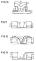
- FIGS. 1 to 13 show an FET in cross section after various method steps.
- only one photographic technology step is used in order to obtain an asymmetrical distance between the gate and the contact layer portions of the source and drain and, if appropriate, to simultaneously generate an additional etching stage (double recess) on the drain side in the transition to the contact layer.
- an effective gate length of 0.2 ⁇ m can be generated based on light-optical lithography.
- a layer sequence of semiconductor material which is customary for field effect transistors is produced with at least layer 1 provided for the gate (see FIG. 1) and then a highly doped contact layer 2 for source and drain. These layers can e.g. B. grown on a semiconductor substrate (z. B. from GaAs) epitaxially.
- the layers can also be produced in the wafer by ion implantation.
- the layer sequence mentioned consists of a channel layer and a highly doped contact layer one above the other, e.g. B. on a semi-insulating GaAs substrate.
- the channel layer and the contact layer can also be GaAs.
- the layer sequence is e.g. B. a buffer layer on a semi-insulating substrate which is very weakly or not at all doped, thereon a further layer forming a heterojunction, then an intermediate layer and finally a highly doped contact layer.
- the substrate is e.g. B. GaAs, as well as the buffer layer and the contact layer.
- the layer forming the heterojunction is e.g. B. AlGaAs.
- the intermediate layer applied on top is GaAs or AlGaAs. These layer sequences are only given as an example; other layer sequences customary for field effect transistors can also be produced.
- the layer 1 shown in the figures denotes the layer or layer sequence arranged between the substrate and the contact layer in each exemplary embodiment.
- a mask 3 is applied to this layer sequence. This happens e.g. B. by applying a dielectric passivation layer over the entire surface (for example PCVD-SiN 0.2 ⁇ m thick). Then an opening of z. B. 0.6 microns length. This dimension of 0.6 ⁇ m is given for the direction in which the source, gate and drain lie in the finished FET. Because the layers of semiconductor material on which this passivation layer was applied are still completely planar, the prerequisites for photolithography for compliance with this dimensioning with the least possible scattering are given. Because of this and because of the easy reproducibility of the conditions under which the subsequent process steps take place, the process according to the invention is always repeatable and is suitable for producing a large number of practically identical FETs.
- the opening in the passivation layer is z. B. etched with CF4-RIE.
- a recess 4 is subsequently etched by opening this mask 3, which is shown in FIG. 1.
- this mask 3 is shown in FIG. 1.
- the contact layer 2 in the region of this opening partially or completely removed and possibly still etched into layer 1, depending on how the layer thicknesses, the current and the threshold voltage of the transistor in question require.
- This recess 4 has a depth of 100 nm, for example. The result of this method step is shown in FIG. 2.
- an auxiliary layer 5 is then applied asymmetrically on the source side by oblique vapor deposition, as shown in FIG.
- the source is drawn on the left and the drain on the right, as is indicated in FIG. 1 with the letters S (source), G (gate) and D (drain) as a representative of all figures.
- this auxiliary layer 5 z. B. metal (aluminum is particularly suitable) evaporated.
- the auxiliary layer can e.g. B. 50 nm thick and the evaporation from an angle of about 45 ° to the layer plane. It is thereby achieved that the auxiliary layer 5 only covers the surface of the layer 1 in the region of the recess 4 on the source side.
- the evaporation of the auxiliary layer 5 is indicated in FIG. 3 with the arrows drawn at an angle.
- spacers are produced on the source side and on the drain side in the opening.
- B. are described in German patent application P 42 11 0 51.3, can be done.
- These spacers are e.g. B. of SiN and have a measured in the plane of Fig. 4 width at the base of about 0.2 microns.
- the thickness of these spacers 6, 7 is chosen so that the source-side spacer 6 is only seated on the auxiliary layer 5.
- the thickness of this auxiliary layer 5 and the direction from which it is vapor-deposited must therefore also be set in the preceding method step with a view to the fact that the source-side spacer 6 produced below must find space on the source-side portion of the auxiliary layer 5.
- the structure according to FIG. 4 is achieved after this method step.
- the spacer 6 on the source side can then be removed by removing the auxiliary layer 5.
- the auxiliary layer 5 is aluminum, it can e.g. B. with liquid HCl (hydrochloric acid). After that, only the spacer 7 on the drain side corresponding to FIG. 5 remains.
- Additional spacers 9 can then be produced on the part of layer 1 that is now exposed. Before this, it is possible to more precisely determine the threshold voltage of the transistor by etching a second recess 8 in layer 1 (see FIG. 6). In order to ensure that this second recess 8 is etched to a predetermined depth, layer 1 can contain a layer sequence with a suitable etching stop layer. This etching stop layer is then arranged at the level of the layer sequence up to which the etching of the second recess 8 is to take place. In this way, the threshold voltage of the transistor can be set in a very reproducible manner.
- FIG. 7 shows a cross section of the FET after the further spacers 9 have been produced on the surface of the layer 1 with the second recess 8.
- the alternative without a second recess 8 is shown in FIG. 9.
- the further spacer on the source side isolates the contact layer 2 on the source side from the gate metallization to be subsequently applied.
- the further spacers 9 are preferably made of the same material as the first spacers (eg SiN). In the present embodiment, these further spacers 9 z. B. with a width of 0.1 microns at the base, ie on the channel layer 1. If you look at the length of 0.6 ⁇ m of the mask opening, the respective dimensions of the spacers at the base points Sutracted, the result is a gate length, ie the length of the surface of layer 1 to be provided with the gate metallization, in the direction from source to drain, of 0.2 ⁇ m.
- the gate metallization 10, 12 and the gate reinforcement 11 are then subsequently applied, the gate reinforcement 11 also serving as an etching mask in order to structure the gate metallization 10, 12.
- the gate metallization 10, 12 is slightly under-etched, so that the metallizations for the source and drain can be applied, as is known from conventional production processes.
- FIGS. 8 and 10 The result after the etching back of the mask 3 down to the source-side and drain-side portions is shown in FIGS. 8 and 10 (example without a second recess 8).
- the gate reinforcement 11 is drawn asymmetrically to the two edges of the contact layer 2 in FIG. 8 or in FIG. 10, although this is not essential for the method according to the invention.
- FIGS. 1 and 2 A second exemplary embodiment is described below in which the auxiliary layer is used as an etching mask.
- the method steps shown in FIGS. 1 and 2 are carried out in this variant in the same way as in the first embodiment. Thereafter, the auxiliary layer is not applied immediately, but first on the channel layer 1 Spacers 6, 7 are produced (see FIG. 11). Then the auxiliary layer 5, the z. B. metal, especially aluminum, but this time evaporated obliquely from the direction of source. This auxiliary layer 5 is applied in such a way that the spacer 7 on the drain is completely covered by this auxiliary layer 5 (see FIG. 12).
- the auxiliary layer 5 can be thicker in this second embodiment than in the first, here z. B. 150 nm.
- the spacer 6 on the source side is removed.
- the material of the auxiliary layer 5 serves as an etching mask, which protects the spacer 7 on the drain side.
- a certain damage to the crystal structure on the surface of the semiconductor material on the source side (near-surface crystal damage) by the RIE can be accepted, since the affected surface layer of layer 1 in a subsequent process step (in the production of a second recess) can be etched away.
- the auxiliary layer 5 has been removed, which when using aluminum z. B. by means of HCL, the arrangement of FIG. 5 results.
- the subsequent method steps correspond to those of FIGS. 6 to 8 or 9 and 10.
Landscapes
- Engineering & Computer Science (AREA)
- Microelectronics & Electronic Packaging (AREA)
- Power Engineering (AREA)
- General Physics & Mathematics (AREA)
- Computer Hardware Design (AREA)
- Physics & Mathematics (AREA)
- Condensed Matter Physics & Semiconductors (AREA)
- Manufacturing & Machinery (AREA)
- Ceramic Engineering (AREA)
- Chemical & Material Sciences (AREA)
- Inorganic Chemistry (AREA)
- Junction Field-Effect Transistors (AREA)
- Electrodes Of Semiconductors (AREA)
- Drying Of Semiconductors (AREA)
Abstract
Description
Die vorliegende Erfindung betrifft ein Verfahren zur Herstellung eines Feldeffekttransistors mit extrem kurzer Gatelänge.The present invention relates to a method for producing a field effect transistor with an extremely short gate length.
Bei Feldeffekttransistoren, insbesondere MESFET's oder HEMT's, soll auf der Source-Seite der Abstand zwischen Gate und Kontaktschicht möglichst klein gehalten werden, damit der parasitäre Source-Widerstand möglichst klein ist. Andererseits soll auf der Drain-Seite der Abstand zwischen Gate und Kontaktschicht relativ groß sein, damit die Durchbruchspannung zwischen Gate und Drain ausreichend groß wird und zugleich die Gate-Drain-Kapazität möglichst klein wird. Bisher wurden zu diesem Zweck selbstjustierende Verfahren eingesetzt, wenn die geforderte Durchbruchspannung nicht zu hoch lag. Dabei blieb der Abstand zwischen dem Gate und der n⁺-Kontaktschicht source- und drainseitig gleich (symmetrische Lage von Source und Drain um das Gate). Für höhere Durchbruchsspannungen wurde mit einem zusätzlichen Fototechnik-Justierschritt auf der Drainseite der Abstand zur Kontaktschicht vergrößert. Derartige Verfahren sind z. B. in den Patentschriften US 4 196 439 und US 4 956 308 beschrieben. In der US 4 300 148 wird vorgeschlagen, die Dicke der aktiven Schicht drainseitig vom Gate so dünn bzw. so niedrig dotiert zu machen, daß sie gerade das Maximum des möglichen Stroms unter dem Gate aufnehmen kann.In field effect transistors, in particular MESFETs or HEMTs, the distance between the gate and the contact layer on the source side should be kept as small as possible so that the parasitic source resistance is as small as possible. On the other hand, the distance between the gate and the contact layer should be relatively large on the drain side, so that the breakdown voltage between the gate and drain is sufficiently large and at the same time the gate-drain capacitance is as small as possible. So far, self-adjusting methods have been used for this purpose if the required breakdown voltage was not too high. The distance between the gate and the n⁺ contact layer remained the same on the source and drain sides (symmetrical position of the source and drain around the gate). For higher breakdown voltages, the distance to the contact layer was increased with an additional photo technology adjustment step on the drain side. Such methods are e.g. B. in the patents US 4 196 439 and US 4 956 308. In US 4,300,148 it is proposed to make the thickness of the active layer on the drain side of the gate so thin or so low that it can absorb just the maximum of the possible current under the gate.
Aufgabe der vorliegenden Erfindung ist es, ein einfach durchführbares Verfahren für die Herstellung eines Feldeffekttransistors mit hoher Durchbruchspannung und kleiner Gate-Drain-Kapazität anzugeben.The object of the present invention is to provide a simple method for producing a field effect transistor with a high breakdown voltage and a smaller one Specify gate-drain capacitance.
Diese Aufgabe wird mit dem Verfahren mit den Merkmalen des Anspruches 1 gelöst. Weitere Ausgestaltungen ergeben sich aus den abhängigen Ansprüchen.This object is achieved with the method having the features of claim 1. Further configurations result from the dependent claims.
Es folgt eine Beschreibung des erfindungsgemäßen Verfahrens anhand der Figuren 1 bis 13, die einen FET im Querschnitt nach verschiedenen Verfahrensschritten zeigen.There follows a description of the method according to the invention with reference to FIGS. 1 to 13, which show an FET in cross section after various method steps.
Bei dem erfindungsgemäßen Verfahren wird nur ein Fototechnikschritt angewendet, um einen unsymmetrischen Abstand des Gate von den Kontaktschichtanteilen von Source und Drain zu erhalten und ggf. zugleich auf der Drainseite eine zusätzliche Ätzstufe (Doppelrecess) im Übergang zur Kontaktschicht zu erzeugen. Außerdem kann ausgehend von einer lichtoptischen Lithographie eine effektive Gate-Länge von 0,2 µm erzeugt werden. Bei diesem Verfahren wird eine für Feldeffekttransistoren übliche Schichtfolge aus Halbleitermaterial mit mindestens der für das Gate vorgesehenen Schicht 1 (s. Fig. 1) und darauf einer hochdotierten Kontaktschicht 2 für Source und Drain hergestellt. Diese Schichten können z. B. auf einem Halbleitersubstrat (z. B. aus GaAs) epitaktisch aufgewachsen werden. Die Schichten können auch in dem Wafer durch Ionenimplantation hergestellt werden. Bei einem ionenimplantierten MESFET besteht die genannte Schichtfolge aus einer Kanalschicht und einer hochdotierten Kontaktschicht übereinander z. B. auf einem semiisolierenden GaAs-Substrat. Die Kanalschicht und die Kontaktschicht können ebenfalls GaAs sein. Bei einem epitaktisch aufgewachsenen HEMT ist die Schichtfolge z. B. eine Pufferschicht auf einem semiisolierenden Substrat, die sehr schwach oder gar nicht dotiert ist, darauf eine einen Heteroübergang bildende weitere Schicht, darauf eine Zwischenschicht und schließlich eine hochdotierte Kontaktschicht. Das Substrat ist z. B. GaAs, ebenso die Pufferschicht und die Kontaktschicht. Die den Heteroübergang bildende Schicht ist z. B. AlGaAs. Die darauf aufgebrachte Zwischenschicht ist GaAs oder AlGaAs. Diese Schichtfolgen sind nur als Beispiel angegeben; es können ebenso gut andere für Feldeffekttransistoren gebräuchliche Schichtfolgen hergestellt werden. Die in den Figuren gezeichnete Schicht 1 bezeichnet in jedem Ausführungsbeispiel die zwischen dem Substrat und der Kontaktschicht angeordnete Schicht oder Schichtfolge.In the method according to the invention, only one photographic technology step is used in order to obtain an asymmetrical distance between the gate and the contact layer portions of the source and drain and, if appropriate, to simultaneously generate an additional etching stage (double recess) on the drain side in the transition to the contact layer. In addition, an effective gate length of 0.2 µm can be generated based on light-optical lithography. In this method, a layer sequence of semiconductor material which is customary for field effect transistors is produced with at least layer 1 provided for the gate (see FIG. 1) and then a highly doped
Auf dieser Schichtfolge wird eine Maske 3 aufgebracht. Das geschieht z. B. durch ganzflächiges Aufbringen einer dielektrischen Passivierungsschicht (z. B. PCVD-SiN 0,2 µm dick). Danach wird in dieser Passivierungsschicht mittels Fototechnik eine Öffnung von z. B. 0,6 µm Länge hergestellt. Diese Bemessung von 0,6 µm ist dabei für die Richtung, in der Source, Gate und Drain bei den fertigen FET liegen, angegeben. Weil die Schichten aus Halbleitermaterial, auf denen diese Passivierungsschicht aufgebracht wurde, noch vollkommen planar sind, sind die Voraussetzungen der Fotolithographie für ein Einhalten dieser Bemessung mit der geringstmöglichen Streuung gegeben. Deswegen und wegen der leichten Reproduzierbarkeit der Bedingungen, unter denen die nachfolgenden Verfahrensschritten ablaufen, ist das erfindungsgemäße Verfahren stets wiederholbar und ist geeignet, eine hohe Stückzahl von praktisch identischen FET's zu produzieren. Die Öffnung in der Passivierungsschicht wird z. B. mit CF₄-RIE geätzt.A
Durch die Öffnung dieser Maske 3, die in Fig. 1 dargestellt ist, wird nachfolgend ein Recess 4 geätzt. Dabei wird z. B. mittels Cl-RIE die Kontaktschicht 2 im Bereich dieser Öffnung teilweise oder ganz entfernt und ggf. noch bis in die Schicht 1 hinein geätzt, je nachdem wie es die Schichtdicken, der Strom und die Einsatzspannung des betreffenden Transistors erfordern. Dieser Recess 4 hat beispielsweise eine Tiefe von 100 nm. Das Ergebnis dieses Verfahrensschrittes ist in Fig. 2 dargestellt.A recess 4 is subsequently etched by opening this
Bei einem ersten Ausführungsbeispiel des erfindungsgemäßen Verfahrens wird dann wie in Fig. 3 gezeigt durch schräges Aufdampfen auf der Source-Seite unsymmetrisch eine Hilfsschicht 5 aufgebracht. In den Figuren sind Source jeweils links und Drain jeweils rechts gezeichnet, wie das in Fig. 1 mit den Buchstaben S (Source), G (Gate) und D (Drain) stellvertretend für alle Figuren bezeichnet ist. Als diese Hilfsschicht 5 wird z. B. Metall (geeignet ist insbesondere Aluminium) aufgedampft. Bei den bisher angegebenen Bemessungen kann die Hilfsschicht z. B. 50 nm dick sein und das Aufdampfen aus einem Winkel von etwa 45° zu der Schichtebene erfolgen. Damit wird erreicht, daß die Hilfsschicht 5 die Oberfläche der Schicht 1 im Bereich des Recess 4 nur sourceseitig bedeckt. Das Aufdampfen der Hilfsschicht 5 ist in Fig. 3 mit den schräg eingezeichneten Pfeilen angedeutet.In a first exemplary embodiment of the method according to the invention, an
In einem weiteren Verfahrensschritt werden Spacer sourceseitig und drainseitig in der Öffnung hergestellt, was mittels eines der üblichen Verfahren, wie sie z. B. in der deutschen Patentanmeldung P 42 11 0 51.3 beschrieben sind, erfolgen kann. Diese Spacer sind z. B. aus SiN und besitzen eine in der Zeichenebene von Fig. 4 gemessene Breite am Fußpunkt von etwa 0,2 µm. Die Dicke dieser Spacer 6, 7 wird dabei so gewählt, daß der sourceseitige Spacer 6 nur auf der Hilfsschicht 5 sitzt. Die Dicke dieser Hilfsschicht 5 und die Richtung, aus der sie aufgedampft wird, ist daher in dem vorhergehenden Verfahrensschritt auch im Hinblick darauf einzustellen, daß der nachfolgend hergestellte sourceseitige Spacer 6 auf dem sourceseitigen Anteil der Hilfsschicht 5 Platz finden muß. Nach diesem Verfahrensschritt ist der Aufbau nach Fig. 4 erreicht. Der sourceseitige Spacer 6 kann dann entfernt werden, indem die Hilfsschicht 5 entfernt wird. Falls die Hilfsschicht 5 Aluminium ist, kann sie z. B. mit flüssigem HCl (Salzsäure) entfernt werden. Es bleibt danach nur der drainseitige Spacer 7 entsprechend Fig. 5.In a further process step, spacers are produced on the source side and on the drain side in the opening. B. are described in German
Auf dem jetzt freiliegenden Anteil der Schicht 1 können dann weitere Spacer 9 hergestellt werden. Zuvor ist es möglich, durch Ätzen eines zweiten Recess 8 in die Schicht 1 die Einsatzspannung des Transistors genauer festzulegen (s. Fig. 6). Um sicherzustellen, daß dieser zweite Recess 8 bis zu einer vorgegebenen Tiefe geätzt wird, kann die Schicht 1 eine Schicht folge mit einer geeigneten Ätzstoppschicht enthalten. Diese Ätzstoppschicht ist dann auf der Höhe der Schichtfolge angeordnet, bis zu der das Ätzen des zweiten Recess 8 erfolgen soll. Auf diese Weise kann die Einsatzspannung des Transistors sehr genau reproduzierbar festgelegt werden. Fig. 7 zeigt einen Querschnitt des FET's nach dem Herstellen der weiteren Spacer 9 auf der Oberfläche der Schicht 1 mit dem zweiten Recess 8.Additional spacers 9 can then be produced on the part of layer 1 that is now exposed. Before this, it is possible to more precisely determine the threshold voltage of the transistor by etching a second recess 8 in layer 1 (see FIG. 6). In order to ensure that this second recess 8 is etched to a predetermined depth, layer 1 can contain a layer sequence with a suitable etching stop layer. This etching stop layer is then arranged at the level of the layer sequence up to which the etching of the second recess 8 is to take place. In this way, the threshold voltage of the transistor can be set in a very reproducible manner. FIG. 7 shows a cross section of the FET after the further spacers 9 have been produced on the surface of the layer 1 with the second recess 8.
Die Alternative ohne zweiten Recess 8 ist in Fig. 9 dargestellt. Der sourceseitige weitere Spacer isoliert insbesondere die Kontaktschicht 2 auf der Source-Seite von der nachfolgend aufzubringenden Gate-Metallisierung. Die weiteren Spacer 9 werden vorzugsweise aus dem gleichen Material wie die ersten Spacer (z. B. SiN) hergestellt. In dem vorliegenden Ausführungsbeispiel werden diese weiteren Spacer 9 z. B. mit einer Breite von 0,1 µm an dem Fußpunkt, d. h. auf der Kanalschicht 1 hergestellt. Wenn man von der Länge von 0,6 µm der Maskenöffnung die jeweiligen Abmessungen der Spacer an den Fußpunkten suttrahiert, resultiert eine Gatelänge, d. h. die Länge der mit der Gate-Metallisierung zu versehenden Oberfläche der Schicht 1 in Richtung von Source nach Drain, von 0,2 µm. Damit ist eine extrem kurze Gatelänge von 0,2 µm bei gleichzeitiger unsymmetrischer Ausrichtung des Gates in bezug auf Source und Drain realisiert.
Nachfolgend werden dann die Gate-Metallisierung 10, 12 und die Gate-Verstärkung 11 aufgebracht, wobei die Gate-Verstärkung 11 zugleich als Ätzmaske dient, um die Gate-Metallisierung 10, 12 zu strukturieren. Beim Ätzen der Maske 3 wird die Gate-Metallisierung 10, 12 geringfügig unterätzt, so daß die Metallisierungen für Source und Drain aufgebracht werden können, wie es von herkömmlichen Herstellungsverfahren her bekannt ist. Das Resultat nach dem Rückätzen der Maske 3 bis auf sourceseitige und drainseitige Anteile ist in Fig. 8 bzw. Fig. 10 (Beispiel ohne zweiten Recess 8) dargestellt.The alternative without a second recess 8 is shown in FIG. 9. The further spacer on the source side, in particular, isolates the
The
Unabhängig von den wesentlichen Schritten der vorliegenden Erfindung sollte bei der Justierung der Gateverstärkung 11 auf der Drainseite darauf geachtet werden, daß die Verstärkung die Kontaktschicht 2 nicht unnötig weit überragt, damit die Drain-Gate-Kapazität klein bleibt. Deswegen ist in Fig. 8 bzw. in Fig. 10 die Gate-Verstärkung 11 unsymmetrisch zu den beiden Kanten der Kontaktschicht 2 gezeichnet, obwohl das für das erfindungsgemäße Verfahren nicht wesentlich ist.Regardless of the essential steps of the present invention, when adjusting the
Es wird im folgenden ein zweites Ausführungsbeispiel beschrieben, bei der die Hilfsschicht als Ätzmaske verwendet wird. Die Verfahrensschritte, die in den Fig. 1 und 2 dargestellt sind, werden bei dieser Variante in der gleichen Weise wie bei dem ersten Ausführungsbeispiel durchgeführt. Danach wird nicht sogleich die Hilfsschicht aufgebracht, sondern zunächst auf der Kanalschicht 1 die Spacer 6, 7 hergestellt (s. Fig. 11). Dann wird die Hilfsschicht 5, die wieder z. B. Metall, insbesondere Aluminium sein kann, diesmal aber schräg aus der Richtung von Source aufgedampft. Dieses Aufbringen der Hilfsschicht 5 erfolgt derart, daß der drainseitige Spacer 7 von dieser Hilfsschicht 5 vollständig abgedeckt wird (s. Fig. 12). Die Hilfsschicht 5 kann in diesem zweiten Ausführungsbeispiel dicker sein als in dem ersten, hier z. B. 150 nm.A second exemplary embodiment is described below in which the auxiliary layer is used as an etching mask. The method steps shown in FIGS. 1 and 2 are carried out in this variant in the same way as in the first embodiment. Thereafter, the auxiliary layer is not applied immediately, but first on the channel layer 1
In einem weiteren Schritt wird der sourceseitige Spacer 6 entfernt. Das geschieht z. B. mittels CF₄-RIE. Das Material der Hilfsschicht 5 dient dabei als Ätzmaske, die den drainseitigen Spacer 7 schützt. Eine gewisse Beschädigung der Kristallstruktur an der Oberfläche des Halbleitermateriales auf der Source-Seite (oberflächennahes Kristall-Damage) durch das RIE kann dabei in Kauf genommen werden, da die betroffene Oberflächenschicht der Schicht 1 in einem nachfolgenden Verfahrensschritt (bei der Herstellung eines zweiten Recess) weggeätzt werden kann. Nachdem die Hilfsschicht 5 entfernt worden ist, was bei Verwendung von Aluminium z. B. mittels HCL geschehen kann, ergibt sich die Anordnung der Fig. 5. Die daran sich anschließenden Verfahrensschritte entsprechen denen der Figuren 6 bis 8 bzw. 9 und 10.In a further step, the
Wesentlich bei dem Verfahren der Erfindung ist es, daß auf der Drain-Seite ein zusätzlicher Spacer hergestellt wird, wodurch erreicht wird, daß die Gate-Metallisierung zur Source-Seite hin verschoben positioniert wird. Dieses Verfahren ist insbesondere vorteilhaft, wenn Transistoren mit extrem kurzer Gate-Länge hergestellt werden sollen (z. B. für hohe Frequenzen). Die deutlichste Verbesserung gegenüber dem Stand der Technik erreicht man damit etwa für Gate-Längen bis 0,4 µm, es kann aber auch für größere Bemessungen angewendet werden.It is essential in the method of the invention that an additional spacer is produced on the drain side, with the result that the gate metallization is positioned so that it is displaced towards the source side. This method is particularly advantageous if transistors with an extremely short gate length are to be produced (e.g. for high frequencies). The most significant improvement over the prior art can be achieved for gate lengths of up to 0.4 µm, but it can also be used for larger dimensions.
Claims (7)
in einem ersten Schritt auf einer Schichtfolge, die mindestens eine für ein Gate vorgesehene Schicht (1) und eine hoch dotierte Kontaktschicht (2) umfaßt, eine Maske (3) mit einer Öffnung im Bereich des herzustellenden Gates aufgebracht wird,
in einem zweiten Schritt ein Recess (4) in diesem Bereich hergestellt wird, indem dort mindestens die Dicke der Kontaktschicht (2) vermindert wird,
in einem dritten Schritt source- und drainseitige Spacer (6, 7) in der Öffnung hergestellt werden,
in einem vierten Schritt der sourceseitige Spacer (6) entfernt wird,
in einem fünften Schritt weitere Spacer (9) hergestellt werden,
in einem sechsten Schritt eine Gate-Metallisierung (10, 12) zwischen diesen weiteren Spacern (9) und durch diese von der Kontaktschicht (2) elektrisch isoliert auf der Kanalschicht (1) aufgebracht wird und Metallisierungen für Source und Drain hergestellt werden.Method for producing a field effect transistor, in which
in a first step, a mask (3) with an opening in the region of the gate to be produced is applied to a layer sequence which comprises at least one layer (1) provided for a gate and a highly doped contact layer (2),
in a second step, a recess (4) is produced in this area by at least reducing the thickness of the contact layer (2) there,
in a third step, source and drain spacers (6, 7) are produced in the opening,
in a fourth step the spacer (6) on the source side is removed,
in a fifth step, further spacers (9) are produced,
in a sixth step, a gate metallization (10, 12) is applied between these further spacers (9) and through this is applied to the channel layer (1) in an electrically insulated manner from the contact layer (2) and metallizations for source and drain are produced.
bei dem
zwischen dem zweiten und dem dritten Schritt eine Hilfsschicht (5) derart aufgebracht wird, daß diese Hilfsschicht (5) in dem Recess (4) nur sourceseitig vorhanden ist,
in dem dritten Schritt der sourceseitige Spacer (6) auf dieser Hilfsschicht (5) hergestellt wird und
der vierte Schritt erfolgt, indem die Hilfsschicht (5) und damit der sourceseitige Spacer (6) entfernt werden.Method according to claim 1,
in which
an auxiliary layer (5) is applied between the second and the third step such that this auxiliary layer (5) is only present in the recess (4) on the source side,
in the third step, the source-side spacer (6) is produced on this auxiliary layer (5) and
the fourth step is carried out by removing the auxiliary layer (5) and thus the source-side spacer (6).
bei dem
zwischen dem dritten und dem vierten Schritt eine Hilfsschicht (5) derart aufgebracht wird, daß nur der drainseitige Spacer (7) von dieser Hilfsschicht (5) vollständig abgedeckt wird,
bei dem diese Hilfsschicht (5) aus einem Material ist, bezüglich dessen der sourceseitige Spacer (6) selektiv entfernt werden kann, und
bei dem zwischen dem vierten Schritt und dem fünften Schritt die Hilfsschicht (5) entfernt wird.Method according to claim 1,
in which
an auxiliary layer (5) is applied between the third and fourth step such that only the drain spacer (7) is completely covered by this auxiliary layer (5),
in which this auxiliary layer (5) is made of a material with respect to which the spacer (6) on the source side can be selectively removed, and
in which the auxiliary layer (5) is removed between the fourth step and the fifth step.
bei dem die Hilfsschicht (5) aus einer Richtung aufgebracht wird, die bezüglich der Senkrechten auf einer die Orientierung der Schicht folge festlegenden Ebene geneigt ist.Method according to claim 2 or 3,
in which the auxiliary layer (5) is applied from a direction which is inclined with respect to the vertical on a plane which determines the orientation of the layer.
bei dem die Hilfsschicht (5) Metall ist.Method according to one of claims 2 to 4,
in which the auxiliary layer (5) is metal.
bei dem vor dem fünften Schritt ein zweiter Recess (8) in der Kanalschicht (1) hergestellt wird.Method according to one of claims 1 to 5,
in which a second recess (8) is produced in the channel layer (1) before the fifth step.
bei dem die Bemessungen der Öffnung in der Maske (3), des drainseitigen Spacers (7) und der weiteren Spacer (9) so vorgenommen werden, daß die Gatelänge, d. h. die Länge der Kontaktfläche zwischen der Gate-Metallisierung (10, 12) und der Kanalschicht (1) in Richtung von Source nach Drain, maximal 0,4 µm beträgt.Method according to one of claims 1 to 6,
in which the dimensions of the opening in the mask (3), the drain-side spacer (7) and the further spacers (9) are carried out such that the gate length, ie the length of the contact area between the gate metallization (10, 12) and the channel layer (1) in the direction from source to drain is a maximum of 0.4 µm.
Applications Claiming Priority (2)
| Application Number | Priority Date | Filing Date | Title |
|---|---|---|---|
| DE4215985 | 1992-05-14 | ||
| DE4215985 | 1992-05-14 |
Publications (1)
| Publication Number | Publication Date |
|---|---|
| EP0569745A1 true EP0569745A1 (en) | 1993-11-18 |
Family
ID=6458899
Family Applications (1)
| Application Number | Title | Priority Date | Filing Date |
|---|---|---|---|
| EP93106507A Withdrawn EP0569745A1 (en) | 1992-05-14 | 1993-04-21 | Method of manufacturing a field effect transistor with asymmetrical gate structure |
Country Status (3)
| Country | Link |
|---|---|
| US (1) | US5298444A (en) |
| EP (1) | EP0569745A1 (en) |
| JP (1) | JPH0637118A (en) |
Cited By (1)
| Publication number | Priority date | Publication date | Assignee | Title |
|---|---|---|---|---|
| FR2740262A1 (en) * | 1995-10-20 | 1997-04-25 | Thomson Csf | FET with offset T=shaped gate |
Families Citing this family (16)
| Publication number | Priority date | Publication date | Assignee | Title |
|---|---|---|---|---|
| US6271547B1 (en) | 1999-08-06 | 2001-08-07 | Raytheon Company | Double recessed transistor with resistive layer |
| US6797994B1 (en) | 2000-02-14 | 2004-09-28 | Raytheon Company | Double recessed transistor |
| WO2003032397A2 (en) * | 2001-07-24 | 2003-04-17 | Cree, Inc. | INSULTING GATE AlGaN/GaN HEMT |
| JP4093395B2 (en) * | 2001-08-03 | 2008-06-04 | 富士通株式会社 | Semiconductor device and manufacturing method thereof |
| KR100424184B1 (en) * | 2002-01-18 | 2004-03-25 | 주식회사 하이닉스반도체 | A method for forming gate of semiconductor device |
| US7071498B2 (en) * | 2003-12-17 | 2006-07-04 | Nitronex Corporation | Gallium nitride material devices including an electrode-defining layer and methods of forming the same |
| DE102005042072A1 (en) * | 2005-06-01 | 2006-12-14 | Forschungsverbund Berlin E.V. | Vertical electrical contact connections e.g. micro-vias, producing method for silicon carbide-wafer, involves laser boring of passage holes through wafer and active layers and applying antiwetting layer in area of openings of holes |
| US7692263B2 (en) | 2006-11-21 | 2010-04-06 | Cree, Inc. | High voltage GaN transistors |
| US8212290B2 (en) | 2007-03-23 | 2012-07-03 | Cree, Inc. | High temperature performance capable gallium nitride transistor |
| CN100585904C (en) * | 2007-12-12 | 2010-01-27 | 中国科学院微电子研究所 | Method for preparing OFET |
| US8946724B1 (en) | 2010-06-02 | 2015-02-03 | Hrl Laboratories, Llc | Monolithically integrated self-aligned GaN-HEMTs and Schottky diodes and method of fabricating the same |
| US9449833B1 (en) * | 2010-06-02 | 2016-09-20 | Hrl Laboratories, Llc | Methods of fabricating self-aligned FETS using multiple sidewall spacers |
| US8383471B1 (en) | 2011-04-11 | 2013-02-26 | Hrl Laboratories, Llc | Self aligned sidewall gate GaN HEMT |
| KR20130123137A (en) * | 2012-05-02 | 2013-11-12 | 에스케이하이닉스 주식회사 | Semiconductor device and method for fabricating the same |
| US10170611B1 (en) | 2016-06-24 | 2019-01-01 | Hrl Laboratories, Llc | T-gate field effect transistor with non-linear channel layer and/or gate foot face |
| US10868162B1 (en) | 2018-08-31 | 2020-12-15 | Hrl Laboratories, Llc | Self-aligned gallium nitride FinFET and method of fabricating the same |
Citations (4)
| Publication number | Priority date | Publication date | Assignee | Title |
|---|---|---|---|---|
| US4956308A (en) * | 1987-01-20 | 1990-09-11 | Itt Corporation | Method of making self-aligned field-effect transistor |
| EP0439114A1 (en) * | 1990-01-24 | 1991-07-31 | Kabushiki Kaisha Toshiba | Compound semiconductor device having gate electrode self-aligned to source and drain electrodes and method of manufacturing the same |
| EP0443348A2 (en) * | 1990-02-23 | 1991-08-28 | Rohm Co., Ltd. | Fine processing method using oblique metal deposition |
| EP0466103A1 (en) * | 1990-07-11 | 1992-01-15 | Siemens Aktiengesellschaft | Method for forming a metallization by evaporation using an oblique direction of incidence on semiconductor material |
Family Cites Families (9)
| Publication number | Priority date | Publication date | Assignee | Title |
|---|---|---|---|---|
| US4196439A (en) * | 1978-07-03 | 1980-04-01 | Bell Telephone Laboratories, Incorporated | Semiconductor device drain contact configuration |
| US4300148A (en) * | 1979-08-10 | 1981-11-10 | Bell Telephone Laboratories, Incorporated | Semiconductor device gate-drain configuration |
| JPS61231770A (en) * | 1985-04-08 | 1986-10-16 | Nec Corp | Manufacture of semiconductor device |
| JPS63207177A (en) * | 1987-02-24 | 1988-08-26 | Toshiba Corp | Manufacture of semiconductor device |
| US5024957A (en) * | 1989-02-13 | 1991-06-18 | International Business Machines Corporation | Method of fabricating a bipolar transistor with ultra-thin epitaxial base |
| US5108939A (en) * | 1990-10-16 | 1992-04-28 | National Semiconductor Corp. | Method of making a non-volatile memory cell utilizing polycrystalline silicon spacer tunnel region |
| JPH04167439A (en) * | 1990-10-30 | 1992-06-15 | Mitsubishi Electric Corp | Manufacture of semiconductor device |
| US5155052A (en) * | 1991-06-14 | 1992-10-13 | Davies Robert B | Vertical field effect transistor with improved control of low resistivity region geometry |
| US5208177A (en) * | 1992-02-07 | 1993-05-04 | Micron Technology, Inc. | Local field enhancement for better programmability of antifuse PROM |
-
1993
- 1993-04-21 EP EP93106507A patent/EP0569745A1/en not_active Withdrawn
- 1993-04-26 US US08/052,549 patent/US5298444A/en not_active Expired - Fee Related
- 1993-05-12 JP JP5133830A patent/JPH0637118A/en not_active Withdrawn
Patent Citations (4)
| Publication number | Priority date | Publication date | Assignee | Title |
|---|---|---|---|---|
| US4956308A (en) * | 1987-01-20 | 1990-09-11 | Itt Corporation | Method of making self-aligned field-effect transistor |
| EP0439114A1 (en) * | 1990-01-24 | 1991-07-31 | Kabushiki Kaisha Toshiba | Compound semiconductor device having gate electrode self-aligned to source and drain electrodes and method of manufacturing the same |
| EP0443348A2 (en) * | 1990-02-23 | 1991-08-28 | Rohm Co., Ltd. | Fine processing method using oblique metal deposition |
| EP0466103A1 (en) * | 1990-07-11 | 1992-01-15 | Siemens Aktiengesellschaft | Method for forming a metallization by evaporation using an oblique direction of incidence on semiconductor material |
Non-Patent Citations (1)
| Title |
|---|
| PATENT ABSTRACTS OF JAPAN vol. 11, no. 77 (E-487)(2524) 7. März 1987 & JP-A-61 231 770 ( NEC ) 16. Oktober 1986 * |
Cited By (1)
| Publication number | Priority date | Publication date | Assignee | Title |
|---|---|---|---|---|
| FR2740262A1 (en) * | 1995-10-20 | 1997-04-25 | Thomson Csf | FET with offset T=shaped gate |
Also Published As
| Publication number | Publication date |
|---|---|
| JPH0637118A (en) | 1994-02-10 |
| US5298444A (en) | 1994-03-29 |
Similar Documents
| Publication | Publication Date | Title |
|---|---|---|
| EP0569745A1 (en) | Method of manufacturing a field effect transistor with asymmetrical gate structure | |
| DE102005059231B4 (en) | A method of fabricating a compound semiconductor field effect transistor having a fin structure and compound semiconductor field effect transistor having a fin structure | |
| EP0237826B1 (en) | Method of making a self-aligned metallic contact | |
| DE2706623C2 (en) | ||
| EP0005461B1 (en) | Metal semiconductor field effect transistor(mesfet)and method for its manufacture | |
| EP0308939B1 (en) | Method of manufacturing a mesfet with self aligned gate | |
| DE3043289C2 (en) | ||
| DE102008060704B4 (en) | Field effect transistor device and method for its production with a composite passivation process | |
| DE3939319A1 (en) | ASYMMETRICAL FIELD EFFECT TRANSISTOR AND METHOD FOR THE PRODUCTION THEREOF | |
| WO2005104238A1 (en) | Fin field effect transistor arrangement and method for producing a fin field effect transistor arrangement | |
| DE3602652C2 (en) | Field effect transistor with heterojunction | |
| DE4138842A1 (en) | GATE ELECTRODE OF A SEMICONDUCTOR DEVICE AND METHOD FOR THE PRODUCTION THEREOF | |
| DE2607898A1 (en) | DOUBLE GATE SCHOTTKY FIELD EFFECT TRANSISTOR WITH INTERMEDIATE ELECTRODE AND PROCESS FOR PRODUCING IT | |
| EP0033003A2 (en) | Double diffused MOS field-effect-transistor and process for its manufacture | |
| EP0394757A2 (en) | Method for fabrication of active semiconductor structures using basic structures with surface-parallel 2D-charge carrier layer | |
| EP0416141A1 (en) | Process for manufacturing an FET having an asymmetrically positioned gate region | |
| DE60037072T2 (en) | Compound semiconductor field effect transistor and its manufacturing method | |
| DE3736009C2 (en) | Junction FET | |
| DE4400233C2 (en) | Field effect transistor | |
| DE2842589A1 (en) | FIELD EFFECT TRANSISTOR WITH REDUCED SUBSTRATE CONTROL OF CHANNEL WIDTH | |
| DE3538855C2 (en) | ||
| EP0429697B1 (en) | Semiconductor wafer with doped kerf-regions | |
| DE2824026A1 (en) | Barrier layer FET - mfd. by under etching bottom mask layer to cover barrier layer surface | |
| EP0823728B1 (en) | Method of manufacturing a field effect transistor | |
| DE3545434C2 (en) | Semiconductor device |
Legal Events
| Date | Code | Title | Description |
|---|---|---|---|
| PUAI | Public reference made under article 153(3) epc to a published international application that has entered the european phase |
Free format text: ORIGINAL CODE: 0009012 |
|
| AK | Designated contracting states |
Kind code of ref document: A1 Designated state(s): DE FR GB IT |
|
| 17P | Request for examination filed |
Effective date: 19931206 |
|
| STAA | Information on the status of an ep patent application or granted ep patent |
Free format text: STATUS: THE APPLICATION IS DEEMED TO BE WITHDRAWN |
|
| 18D | Application deemed to be withdrawn |
Effective date: 19951101 |