EP0556085B1 - Connection assembly between a motherboard and a daugtherboard - Google Patents
Connection assembly between a motherboard and a daugtherboard Download PDFInfo
- Publication number
- EP0556085B1 EP0556085B1 EP93400249A EP93400249A EP0556085B1 EP 0556085 B1 EP0556085 B1 EP 0556085B1 EP 93400249 A EP93400249 A EP 93400249A EP 93400249 A EP93400249 A EP 93400249A EP 0556085 B1 EP0556085 B1 EP 0556085B1
- Authority
- EP
- European Patent Office
- Prior art keywords
- connector
- insulating body
- connection
- connection assembly
- assembly according
- Prior art date
- Legal status (The legal status is an assumption and is not a legal conclusion. Google has not performed a legal analysis and makes no representation as to the accuracy of the status listed.)
- Expired - Lifetime
Links
Images

Classifications
-
- H—ELECTRICITY
- H01—ELECTRIC ELEMENTS
- H01R—ELECTRICALLY-CONDUCTIVE CONNECTIONS; STRUCTURAL ASSOCIATIONS OF A PLURALITY OF MUTUALLY-INSULATED ELECTRICAL CONNECTING ELEMENTS; COUPLING DEVICES; CURRENT COLLECTORS
- H01R12/00—Structural associations of a plurality of mutually-insulated electrical connecting elements, specially adapted for printed circuits, e.g. printed circuit boards [PCB], flat or ribbon cables, or like generally planar structures, e.g. terminal strips, terminal blocks; Coupling devices specially adapted for printed circuits, flat or ribbon cables, or like generally planar structures; Terminals specially adapted for contact with, or insertion into, printed circuits, flat or ribbon cables, or like generally planar structures
- H01R12/70—Coupling devices
- H01R12/7005—Guiding, mounting, polarizing or locking means; Extractors
-
- Y—GENERAL TAGGING OF NEW TECHNOLOGICAL DEVELOPMENTS; GENERAL TAGGING OF CROSS-SECTIONAL TECHNOLOGIES SPANNING OVER SEVERAL SECTIONS OF THE IPC; TECHNICAL SUBJECTS COVERED BY FORMER USPC CROSS-REFERENCE ART COLLECTIONS [XRACs] AND DIGESTS
- Y10—TECHNICAL SUBJECTS COVERED BY FORMER USPC
- Y10S—TECHNICAL SUBJECTS COVERED BY FORMER USPC CROSS-REFERENCE ART COLLECTIONS [XRACs] AND DIGESTS
- Y10S439/00—Electrical connectors
- Y10S439/948—Contact or connector with insertion depth limiter
Definitions
- the subject of the present invention is a connection set between a motherboard and a card girl.
- a set of connection between a motherboard and a daughterboard comprising a first connector comprising a first insulating body having first elements of contact whose first end is intended to be inserted into a motherboard as well as a second connector comprising a second insulating body having second contact elements including one first end is intended to cooperate with a second end of said contact elements correspondents and a second end of which is intended to be inserted in a daughter card, one side of connection of the first and second insulating body being opposite when the first and the second connector are connected.
- connection set cannot be used only for at most two different card thicknesses girl.
- circuit boards printed in different thicknesses for example 1.6 mm, 2.4 mm, and 3.2 mm. It is not currently possible to treat all possible cases with a single connector width, so that a standardization of models is not possible, hence disadvantages due to the manufacturing costs of connectors of different widths and storage of different types of connectors, which make little interesting the use of such connectors for high thickness printed circuits (3.2 mm in the example above).
- Patent application EP-A-0 392 629 (Van Woensel) describes a example of connection assembly according to known art.
- the subject of the invention is a set of connection of the aforementioned type making it possible to remedy the aforementioned drawback.
- connection assembly is for this purpose characterized in that it comprises a wedging device for maintaining a distance determined between said connection faces of the first and the second insulating body so that a end of daughter board spaced first insulating body, in particular for keeping between the end of the daughter card and the installation plan of the motherboard, a distance equal to the standard dimension connectors of the prior art. Said end of the daughter card is thinned. This allows in particular to separate the second connector from the first connector (male) so that the first row of connection either in one part unthinned daughter card.
- a lateral branch of the first insulating body has at a distal end a housing arranged on its face internal and intended to receive said end thinned, said distance being such that when the first and second connector are connected, an edge of the daughter card is located immediate proximity of said distal end.
- a side face of the second insulating body then has means for holding said end thinned out daughter card.
- the wedging device is also an element of foolproof.
- a timing device may include a patch on at least one said insulating body and / or a projecting element forming an integral part of minus a so-called connection face.
- An insulating body in particular the first body insulator, can have a central part and two lateral branches, the inner side of the part central unit constituting a said connection face.
- Said unthinned edge can be located at immediate proximity of a second end of said connection elements. This keeps a fixation effective of the daughter card on the second body insulating which avoids the constraints on the second ends of the second connection elements.
- a connection assembly has a male connector 3 having a body insulator 10 with a flattened U-shaped profile and a female connector 5 having a central body insulator 81.
- the insulating body 10 includes a region central 11 and two lateral branches 12 and 13, the branch referenced 12 comprising means for foolproof.
- the central region 11 has a plurality of contact elements 60 having a region 61 united with the central region 11, a region 63 forcibly inserted ("press-fit") into motherboard 1, and a male contact region 62 projecting from one side connection 31 of the central region 11.
- the insulating central body 81 has contact elements 85 having a region 83 of female contact set back from one face of connection 41 and connection 88 with forced insertion ("press-fit") in a daughter card 2.
- the elements 85 have a bent region 87 arranged in a zone insulating rear 89 of the insulating body 81.
- a pawn of centering and holding 20 carried by a lateral face 82 of the insulating body 81 allows to solarize a end 25 of daughter card 2 with central body insulator 81.
- a housing 16 located at the distal part 17 of branch 12 can receive the end of the pawn 20.
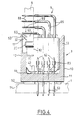
- Figure 2 shows a set of connection which allows, according to the invention, the setting in artwork of a daughter card 6 of greater thickness.
- One or more grooves 42 of the insulating body 81 allow to receive a shim of thickness 40.
- An insert of thickness 40 added is housed removably in the central region 11 or in the central insulating body 81 so that when connectors 3 and 5 are assembled on faces 31 and 41 are spaced from each other. This allows offset the two connectors longitudinally assembled 3 and 5 so that the end 62 of daughter card 6 is spaced from distal end 53 of the arm 12. The position of the end 70 of the card girl remains unchanged.
- the end 61 of the card girl 6 is thinned.
- the proximal part 63 of the end 61 is extended by a connecting edge 62 with the unthinned end 66 of the daughter card 6.
- This end 66 is located in the immediate vicinity of a row 89 of connections 88 and close to the end 53 of the arm 12.
- the shim 40 thus allows to maintain the row 89 of contacts 88 in an unthinned region of the daughter card 6 and at closer to the distal end (here chamfered) of branch 12.
- shim of reported thickness 40 also as a means of coding.
- Keying elements are known, in particular from the request for European patent EP-A-0392629 (Van Woensel) cited above.
- a such wedge is compatible with housing such as 42 (fig. 2 to 4).
- An attached shim 40 makes it possible to adapt easily a standard connection set to all the thicknesses of the daughter card. Additionally, as noted above, it may or may not fulfill a function of keying, which gives great flexibility of use at low cost.
- the shim 44 is an integral part of central region 11 (or of the insulating central body 81). In this case, the whole connection is in principle provided for a thickness maximum given from daughter card 6. It is however possible to also use a shim removable insert to adapt to other daughter card thicknesses 6.
Landscapes
- Details Of Connecting Devices For Male And Female Coupling (AREA)
- Coupling Device And Connection With Printed Circuit (AREA)
Description
La présente invention a pour objet un ensemble de connexion entre une carte mère et une carte fille.The subject of the present invention is a connection set between a motherboard and a card girl.
On connait de l'art antérieur un ensemble de connexion entre une carte mère et une carte fille, comprenant un premier connecteur comportant un premier corps isolant présentant des premiers éléments de contact dont une première extrémité est destinée à être insérée dans une carte mère ainsi qu'un deuxième connecteur comportant un deuxième corps isolant présentant des deuxièmes éléments de contact dont une première extrémité est destinée à coopérer avec une deuxième extrémité desdits éléments de contact correspondants et dont une deuxième extrémité est destinée à être insérée dans une carte fille, une face de connexion du premier et du deuxième corps isolant étant en vis-à-vis lorsque le premier et le deuxième connecteur sont connectés.We know from the prior art a set of connection between a motherboard and a daughterboard, comprising a first connector comprising a first insulating body having first elements of contact whose first end is intended to be inserted into a motherboard as well as a second connector comprising a second insulating body having second contact elements including one first end is intended to cooperate with a second end of said contact elements correspondents and a second end of which is intended to be inserted in a daughter card, one side of connection of the first and second insulating body being opposite when the first and the second connector are connected.
Un tel ensemble de connexion n'est utilisable que pour au plus deux épaisseurs différentes de carte fille. Il existe cependant des cartes de circuit imprimé de différentes épaisseurs, par exemple 1,6 mm, 2,4 mm, et 3,2 mm. Il n'est pas actuellement possible de traiter tous les cas possibles avec une seule largeur de connecteur, ce qui fait qu'une standardisation des modèles n'est pas possible, d'où des inconvénients dûs aux coûts de fabrication de connecteurs de largeurs différentes et au stockage de différents types de connecteurs, qui rendent peu intéressante l'utilisation de tels connecteurs pour des circuits imprimés d'épaisseur élevée (3,2 mm dans l'exemple ci-dessus). Such a connection set cannot be used only for at most two different card thicknesses girl. There are however circuit boards printed in different thicknesses, for example 1.6 mm, 2.4 mm, and 3.2 mm. It is not currently possible to treat all possible cases with a single connector width, so that a standardization of models is not possible, hence disadvantages due to the manufacturing costs of connectors of different widths and storage of different types of connectors, which make little interesting the use of such connectors for high thickness printed circuits (3.2 mm in the example above).
La demande de brevet EP-A-0 392 629 (Van Woensel) décrit un exemple d'ensemble de connexion selon l'art connu. Patent application EP-A-0 392 629 (Van Woensel) describes a example of connection assembly according to known art.
L'invention a pour objet un ensemble de connexion du type précité permettant de remédier à l'inconvénient précité.The subject of the invention is a set of connection of the aforementioned type making it possible to remedy the aforementioned drawback.
L'ensemble de connexion selon l'invention est dans ce but caractérisé en ce qu'il comporte un dispositif de calage destiné à maintenir une distance déterminée entre lesdites faces de connexion du premier et du deuxième corps isolants de telle sorte qu'une extrémité de la carte fille reste espacée du premier corps isolant, notamment pour conserver entre l'extrémité de la carte fille et le plan de pose de la carte mère, une distance égale à la dimension standard des connecteurs de l'art antérieur. Ladite extrémité de la carte fille est amincie. Ceci permet en particulier d'écarter le deuxième connecteur du premieur connecteur (mâle) de telle sorte que la première rangée de raccordement soit dans une partie non amincie de la carte fille.The connection assembly according to the invention is for this purpose characterized in that it comprises a wedging device for maintaining a distance determined between said connection faces of the first and the second insulating body so that a end of daughter board spaced first insulating body, in particular for keeping between the end of the daughter card and the installation plan of the motherboard, a distance equal to the standard dimension connectors of the prior art. Said end of the daughter card is thinned. This allows in particular to separate the second connector from the first connector (male) so that the first row of connection either in one part unthinned daughter card.
Une branche latérale du premier corps isolant présente à une extrémité distale un logement disposé sur sa face interne et destiné à recevoir ladite extrémité amincie, ladite distance étant telle que, lorsque le premier et le deuxième connecteur sont connectés, un bord de la carte fille soit situé à proximité immédiate de ladite extrémité distale. Une face latérale du deuxième corps isolant présente alors un moyen de maintien de ladite extrémité amincie de la carte fille.A lateral branch of the first insulating body has at a distal end a housing arranged on its face internal and intended to receive said end thinned, said distance being such that when the first and second connector are connected, an edge of the daughter card is located immediate proximity of said distal end. A side face of the second insulating body then has means for holding said end thinned out daughter card.
Selon un mode de réalisation avantageux, le dispositif de calage est également un élément de détrompage.According to an advantageous embodiment, the wedging device is also an element of foolproof.
Un dispositif de calage peut comporter une pièce rapportée sur au moins un dit corps isolant et/ou un élément en saillie faisant partie intégrante d'au moins une dite face de connexion.A timing device may include a patch on at least one said insulating body and / or a projecting element forming an integral part of minus a so-called connection face.
Un corps isolant, notamment le premier corps isolant, peut présenter une partie centrale et deux branches latérales, la face interne de la partie centrale constituant une dite face de connexion. An insulating body, in particular the first body insulator, can have a central part and two lateral branches, the inner side of the part central unit constituting a said connection face.
Ledit bord non aminci peut être situé à proximité immédiate d'une deuxième extrémité de dits éléments de connexion. On conserve ainsi une fixation efficace de la carte fille sur le deuxième corps isolant ce qui évite les contraintes sur les deuxièmes extrémités des deuxièmes éléments de connexion.Said unthinned edge can be located at immediate proximity of a second end of said connection elements. This keeps a fixation effective of the daughter card on the second body insulating which avoids the constraints on the second ends of the second connection elements.
D'autres avantages apparaítront à la lecture de la description d'un mode de réalisation de l'invention qui va suivre, donnée à titre d'exemple non limitatif, en liaison avec les dessins qui représentent:
- la figure 1, un ensemble de connexion selon l'art antérieur;
- la figure 2, un ensemble de connexion selon un mode préféré de réalisation de l'invention;
- et les figures 3 et 4, un ensemble de connexion selon une variante de l'invention, respectivement en cours de connexion et après connexion.
- Figure 1, a connection assembly according to the prior art;
- Figure 2, a connection assembly according to a preferred embodiment of the invention;
- and Figures 3 and 4, a connection assembly according to a variant of the invention, respectively during connection and after connection.
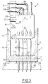
Selon la figure 1, un ensemble de connexion
comporte un connecteur mâle 3 présentant un corps
isolant 10 à profil en forme de U aplati et un
connecteur femelle 5 présentant un corps central
isolant 81. According to Figure 1, a connection assembly
has a
Le corps isolant 10 comprend une région
centrale 11 et deux branches latérales 12 et 13, la
branche référencée 12 comprenant des moyens de
détrompage. Le région centrale 11 comporte une
pluralité d'éléments de contact 60 présentant une
région 61 solidaire de la région centrale 11,une région
63 insérée à force ("press-fit") dans la carte mère 1,
et une région de contact mâle 62 dépassant d'une face
de connexion 31 de la région centrale 11.The
Le corps central isolant 81 présente des
éléments de contact 85 présentant une région 83 de
contact femelle disposée en retrait d'une face de
connexion 41 et un raccordement 88 à insertion forcée
("press-fit") dans une carte fille 2. Les éléments 85
présentent une région coudée 87 disposée dans une zone
arrière isolante 89 du corps isolant 81. Un pion de
centrage et de maintien 20 porté par une face latérale
82 du corps isolant 81 permet de solaridariser une
extrémité 25 de la carte fille 2 avec le corps central
isolant 81. Un logement 16 situé à la partie distale 17
de la branche 12 permet de recevoir l'extrémité du pion
20.The insulating
La figure 2 représente un ensemble de
connexion qui permet, selon l'invention, la mise en
oeuvre d'une carte fille 6 de plus grande épaisseur.Figure 2 shows a set of
connection which allows, according to the invention, the setting in
artwork of a
Une ou plusieurs rainures 42 du corps isolant
81 permettent de recevoir une cale d'épaisseur 40.One or
Une cale d'épaisseur 40 rapportée est logée
de manière amovible dans la région centrale 11 ou dans
le corps central isolant 81 de telle sorte que, lorsque
les connecteurs 3 et 5 sont assemblés les faces 31 et
41 soient espacées l'une de l'autre. Ceci permet de
décaler longitudinalement les deux connecteurs
assemblés 3 et 5 de telle sorte que l'extrémité 62 de
la carte fille 6 soit espacée de l'extrémité distale 53
du bras 12. La position de l'extrémité 70 de la carte
fille reste inchangée.An insert of
Sur les dessins, l'extrémité 61 de la carte
fille 6 est amincie. La partie proximale 63 de
l'extrémité 61 se prolonge par un bord de raccordement
62 avec l'extrémité non amincie 66 de la carte fille 6.
Cette extrémité 66 se situe au voisinage immédiat d'une
rangée 89 de raccordements 88 et à proximité de
l'extrémité 53 du bras 12. La cale d'épaisseur 40
permet ainsi de maintenir la rangée 89 de contacts 88
dans une région non amincie de la carte fille 6 et au
plus près de l'extrémité distale (ici chanfreinée) de
la branche 12.In the drawings, the
On notera en outre qu'il est préféré
d'utiliser la cale d'épaisseur rapportée 40 également
comme moyen de détrompage. Des éléments de détrompage
rapportés sont connus, notamment de la demande de
brevet européen EP-A-0392629 (Van Woensel) précitée. En outre, une
telle cale est compatible avec les logements tels que
42 (fig. 2 à 4).Note also that it is preferred
to use the shim of reported
Une cale rapportée 40 permet d'adapter
facilement un ensemble de connexion standard à toutes
les épaisseurs de carte fille. En outre, comme indiqué
ci-dessus, elle peut ou non remplir une fonction de
détrompage, ce qui confère une grande souplesse
d'utilisation à faible coût.An attached
Selon les figures 3 et 4, la cale d'épaisseur
44 fait partie intégrante de la région centrale 11 (ou
du corps central isolant 81). Dans ce cas, l'ensemble
de connexion est en principe prévu pour une épaisseur
maximale donnée de la carte fille 6. Il est cependant
possible de mettre en oeuvre également une cale
rapportée amovible pour réaliser une adaptation à
d'autres épaisseurs de carte fille 6.According to Figures 3 and 4, the
Selon les figures 1 à 4, on notera également
que la distance entre le bord 70 de la carte 6 et le
plan de pose 71 de la carte 1 est le même dans le cas
de la figure 1 représentant l'art antérieur pour des
épaisseurs de carte 2 allant jusqu'à 2,4 mm, et des
figures 2 à 4 représentant un système de connexion pour
une carte 6 d'épaisseur 3,2 mm.According to Figures 1 to 4, we will also note
that the distance between the
Claims (8)
- Connection assembly between a motherboard (1) and a daughterboard (6), comprising a first connector (3) which includes a first insulating body (10) having first contact elements (60), a first end (63) of which is intended to be inserted into a motherboard (1), and a second connector (5) which includes a second insulating body (81) having second contact elements (85), a first end (83) of which is intended to engage with a second end (62) of the said corresponding first contact elements (60) and a second end (88) of which is intended to be inserted into a daughterboard (6), a connection face (31, 41) of the first insulating body (10) and of the second insulating body (81) facing each other when the first connector (3) and the second connector (5) are connected together, an end (61) of the daughterboard (6) being inserted into a housing lying between a side face (82) of the second insulating body (81) and a side branch (12) of the first insulating body (10), characterized in that it includes a spacing device (40, 44) intended to keep a defined distance between the said connection faces (31, 41) of the first (10) and second (81) insulating bodies in such a way that an end (61) of the daughterboard (6) remains separated from the first insulating body (10), in that the said end (61) of the daughterboard (6) is thinned and in that the said defined distance is such that, when the first connector (3) and the second connector (5) are connected together, a non-thinned edge (66) of the daughterboard (6) lies in the immediate vicinity of the distal end (53) of the side branch (12) of the first insulating body (10).
- Connection assembly according to Claim 1, characterized in that the said spacing device also constitutes a polarization element (40).
- Connection assembly according to either of Claims 1 and 2, characterized in that the spacing device includes at least one piece (40) added onto at least one said insulating body (10, 81).
- Connection assembly according to one of the preceding claims, characterized in that the spacing device includes at least one projecting element (44) forming an integral part of at least one said connection face (31, 41).
- Connection assembly according to one of the preceding claims, characterized in that a said insulating body (10) has a central part (11) and two side branches (12, 13), the internal face of the central part (11) constituting a said connection face (31).
- Connection assembly according to one of the preceding claims, characterized in that a said side branch (12) has, at a distal end (17), a housing (16) located on its internal face opposite the said end (61) of the daughterboard (6) when the first connector (3) and second connector (5) are connected together.
- Connection assembly according to one of the preceding claims, characterized in that the said non-thinned edge (66) lies in the immediate vicinity of a second end (88) of said second connection elements (85).
- Connection assembly according to one of the preceding claims, characterized in that the first connector (3) is a male connector and in that the second connector (5) is a female connector.
Applications Claiming Priority (2)
| Application Number | Priority Date | Filing Date | Title |
|---|---|---|---|
| FR9201618A FR2687508B1 (en) | 1992-02-13 | 1992-02-13 | CONNECTION ASSEMBLY BETWEEN A MOTHER CARD AND A GIRL CARD. |
| FR9201618 | 1992-02-13 |
Publications (2)
| Publication Number | Publication Date |
|---|---|
| EP0556085A1 EP0556085A1 (en) | 1993-08-18 |
| EP0556085B1 true EP0556085B1 (en) | 1998-04-29 |
Family
ID=9426607
Family Applications (1)
| Application Number | Title | Priority Date | Filing Date |
|---|---|---|---|
| EP93400249A Expired - Lifetime EP0556085B1 (en) | 1992-02-13 | 1993-02-02 | Connection assembly between a motherboard and a daugtherboard |
Country Status (4)
| Country | Link |
|---|---|
| US (1) | US5443401A (en) |
| EP (1) | EP0556085B1 (en) |
| DE (1) | DE69318199T2 (en) |
| FR (1) | FR2687508B1 (en) |
Families Citing this family (9)
| Publication number | Priority date | Publication date | Assignee | Title |
|---|---|---|---|---|
| US5443398A (en) * | 1994-01-31 | 1995-08-22 | Robinson Nugent, Inc. | Inverse backplane connector system |
| US6551123B1 (en) * | 1995-02-10 | 2003-04-22 | Marquardt Gmbh | Guiding arrangement for a plug-in battery pack operating an electric appliance |
| TW491425U (en) * | 2000-12-21 | 2002-06-11 | Hon Hai Prec Ind Co Ltd | Electrical connector assembly with a device for preventing erroneous insertion |
| US6979202B2 (en) | 2001-01-12 | 2005-12-27 | Litton Systems, Inc. | High-speed electrical connector |
| US6843657B2 (en) | 2001-01-12 | 2005-01-18 | Litton Systems Inc. | High speed, high density interconnect system for differential and single-ended transmission applications |
| US6910897B2 (en) | 2001-01-12 | 2005-06-28 | Litton Systems, Inc. | Interconnection system |
| US6592382B2 (en) | 2001-12-17 | 2003-07-15 | Woody Wurster | Simplified board connector |
| US6884091B1 (en) * | 2004-04-19 | 2005-04-26 | Component Equipment Company, Inc. | Electrical connector assembly |
| US8690588B2 (en) * | 2011-12-20 | 2014-04-08 | Yazaki North America, Inc. | Junction box assembly having an over-travel spring |
Family Cites Families (12)
| Publication number | Priority date | Publication date | Assignee | Title |
|---|---|---|---|---|
| US3614714A (en) * | 1969-11-21 | 1971-10-19 | Rca Corp | Edge connector with polarizing member |
| JPS5828717B2 (en) * | 1979-08-31 | 1983-06-17 | 富士通株式会社 | polarized connector |
| US4531795A (en) * | 1983-03-01 | 1985-07-30 | Aries Electronics, Inc. | Ejector socket for DIP jumpers |
| FR2553588B1 (en) * | 1983-10-14 | 1986-01-03 | Telecommunications Sa | CONNECTION DEVICE FOR A PRINTED CIRCUIT TEST |
| US4533203A (en) * | 1983-12-07 | 1985-08-06 | Amp Incorporated | Connector for printed circuit boards |
| JPS6197557A (en) * | 1984-10-19 | 1986-05-16 | Kawasaki Steel Corp | Secondary ion mass spectrometer |
| DE3603250A1 (en) * | 1986-02-03 | 1987-08-06 | Allied Corp | Plug connecter, an insulating body for it, and a method for attaching the plug connecter to a printed circuit board |
| US4773881A (en) * | 1987-05-21 | 1988-09-27 | Amp Incorporated | Keying system for connector assemblies |
| NL8900947A (en) * | 1989-04-14 | 1990-11-01 | Du Pont Nederland | CONNECTOR ASSEMBLY. |
| EP0397057B1 (en) * | 1989-05-12 | 1994-07-27 | Siemens Aktiengesellschaft | Assembly for the mechanical and electrical connection of an extension circuit board to a mother circuit board |
| JPH0388289A (en) * | 1989-08-31 | 1991-04-12 | Fujitsu Ltd | Connector for print board |
| FR2685556B1 (en) * | 1991-12-23 | 1994-03-25 | Souriau & Cie | MODULAR ELEMENT FOR ELECTRICAL CONNECTION. |
-
1992
- 1992-02-13 FR FR9201618A patent/FR2687508B1/en not_active Expired - Fee Related
-
1993
- 1993-02-02 EP EP93400249A patent/EP0556085B1/en not_active Expired - Lifetime
- 1993-02-02 DE DE69318199T patent/DE69318199T2/en not_active Expired - Fee Related
-
1994
- 1994-10-27 US US08/331,143 patent/US5443401A/en not_active Expired - Fee Related
Also Published As
| Publication number | Publication date |
|---|---|
| DE69318199D1 (en) | 1998-06-04 |
| DE69318199T2 (en) | 1998-10-22 |
| FR2687508B1 (en) | 1994-11-04 |
| EP0556085A1 (en) | 1993-08-18 |
| US5443401A (en) | 1995-08-22 |
| FR2687508A1 (en) | 1993-08-20 |
Similar Documents
| Publication | Publication Date | Title |
|---|---|---|
| EP0556085B1 (en) | Connection assembly between a motherboard and a daugtherboard | |
| FR2789811A1 (en) | COAXIAL CONNECTION TO CONNECT TWO PRINTED CIRCUIT BOARDS | |
| EP0635167B1 (en) | Disconnectable male connector for use in a communication network | |
| FR2711452A1 (en) | Connection element comprising an insulating bridge. | |
| FR2504316A1 (en) | ELECTRIC CONTACT | |
| AU711843B2 (en) | A coaxial connector and method for fixing this connector to a circuit board | |
| FR2502407A1 (en) | HOLDING AND GUIDING DEVICE FOR CONNECTOR ELBOW PINS | |
| FR2509538A1 (en) | ELECTRICAL CONNECTION BOX | |
| FR2716039A1 (en) | Coaxial electrical connector also performing a switching function. | |
| FR2484718A3 (en) | ELECTRICAL CONNECTOR ASSEMBLY AND DEVICE FOR RELIEVING STRESS WIRES | |
| FR2750261A1 (en) | CONNECTION STRUCTURE FOR A FLAT CIRCUIT BODY AND A CONNECTOR | |
| FR2859826A1 (en) | MEMORY CARD CONNECTOR FOR MOUNTING ON A PRINTED CIRCUIT BOARD | |
| EP0593336B1 (en) | Fastener for releasably fastening a support plate to a component and a connector comprising such a fastener | |
| FR2478383A1 (en) | ELECTRICAL CONTACT MEMBER FOR CONNECTING WITH A MALE CONTACT MEMBER, AND ELECTRICAL CONNECTOR COMPRISING SUCH A CONTACT MEMBER | |
| JP3358156B2 (en) | Connector to be inserted into movable connector | |
| FR3066901B1 (en) | SYSTEM FOR SOLIDARIZING TWO MEDICAL PINS | |
| FR2779013A1 (en) | WELDING CLIP FOR CONNECTOR WITH ELBOW CONTACTS | |
| EP1528631B1 (en) | Solderless connection system for printed circuits | |
| EP0247945B1 (en) | Electrical connecting device between two parts, particularly for the supply of logometers in motor vehicles | |
| WO2005114793A1 (en) | Electric contact and the part od an electric connector comprising said contact | |
| EP0865639B1 (en) | Housing for an extended-format releasable plug-in card | |
| FR2850797A1 (en) | Coaxial cable and printed circuit board connector for wireless transmission system, has cover fixed on printed circuit board and arranged to recover side clearance, on each side of base, formed by locking blade | |
| FR2657491A1 (en) | Lightning arrester for modular assembly and associated modular element | |
| BE1001862A4 (en) | Connecting block telephone type of laminar. | |
| EP0977315A3 (en) | Card edge connector |
Legal Events
| Date | Code | Title | Description |
|---|---|---|---|
| PUAI | Public reference made under article 153(3) epc to a published international application that has entered the european phase |
Free format text: ORIGINAL CODE: 0009012 |
|
| AK | Designated contracting states |
Kind code of ref document: A1 Designated state(s): BE DE ES GB IT NL SE |
|
| 17P | Request for examination filed |
Effective date: 19931029 |
|
| 17Q | First examination report despatched |
Effective date: 19950621 |
|
| GRAG | Despatch of communication of intention to grant |
Free format text: ORIGINAL CODE: EPIDOS AGRA |
|
| GRAG | Despatch of communication of intention to grant |
Free format text: ORIGINAL CODE: EPIDOS AGRA |
|
| GRAH | Despatch of communication of intention to grant a patent |
Free format text: ORIGINAL CODE: EPIDOS IGRA |
|
| GRAH | Despatch of communication of intention to grant a patent |
Free format text: ORIGINAL CODE: EPIDOS IGRA |
|
| GRAA | (expected) grant |
Free format text: ORIGINAL CODE: 0009210 |
|
| AK | Designated contracting states |
Kind code of ref document: B1 Designated state(s): BE DE ES GB IT NL SE |
|
| PG25 | Lapsed in a contracting state [announced via postgrant information from national office to epo] |
Ref country code: GB Free format text: LAPSE BECAUSE OF FAILURE TO SUBMIT A TRANSLATION OF THE DESCRIPTION OR TO PAY THE FEE WITHIN THE PRESCRIBED TIME-LIMIT Effective date: 19980429 Ref country code: ES Free format text: THE PATENT HAS BEEN ANNULLED BY A DECISION OF A NATIONAL AUTHORITY Effective date: 19980429 |
|
| REF | Corresponds to: |
Ref document number: 69318199 Country of ref document: DE Date of ref document: 19980604 |
|
| ITF | It: translation for a ep patent filed |
Owner name: STUDIO TORTA S.R.L. |
|
| PG25 | Lapsed in a contracting state [announced via postgrant information from national office to epo] |
Ref country code: SE Free format text: LAPSE BECAUSE OF FAILURE TO SUBMIT A TRANSLATION OF THE DESCRIPTION OR TO PAY THE FEE WITHIN THE PRESCRIBED TIME-LIMIT Effective date: 19980729 |
|
| GBV | Gb: ep patent (uk) treated as always having been void in accordance with gb section 77(7)/1977 [no translation filed] |
Effective date: 19980429 |
|
| PLBE | No opposition filed within time limit |
Free format text: ORIGINAL CODE: 0009261 |
|
| STAA | Information on the status of an ep patent application or granted ep patent |
Free format text: STATUS: NO OPPOSITION FILED WITHIN TIME LIMIT |
|
| 26N | No opposition filed | ||
| PGFP | Annual fee paid to national office [announced via postgrant information from national office to epo] |
Ref country code: NL Payment date: 20010228 Year of fee payment: 9 |
|
| PGFP | Annual fee paid to national office [announced via postgrant information from national office to epo] |
Ref country code: BE Payment date: 20020221 Year of fee payment: 10 |
|
| PGFP | Annual fee paid to national office [announced via postgrant information from national office to epo] |
Ref country code: DE Payment date: 20020430 Year of fee payment: 10 |
|
| PG25 | Lapsed in a contracting state [announced via postgrant information from national office to epo] |
Ref country code: NL Free format text: LAPSE BECAUSE OF NON-PAYMENT OF DUE FEES Effective date: 20020901 |
|
| NLV4 | Nl: lapsed or anulled due to non-payment of the annual fee |
Effective date: 20020901 |
|
| PG25 | Lapsed in a contracting state [announced via postgrant information from national office to epo] |
Ref country code: BE Free format text: LAPSE BECAUSE OF NON-PAYMENT OF DUE FEES Effective date: 20030228 |
|
| PG25 | Lapsed in a contracting state [announced via postgrant information from national office to epo] |
Ref country code: DE Free format text: LAPSE BECAUSE OF NON-PAYMENT OF DUE FEES Effective date: 20030902 |
|
| PG25 | Lapsed in a contracting state [announced via postgrant information from national office to epo] |
Ref country code: IT Free format text: LAPSE BECAUSE OF NON-PAYMENT OF DUE FEES;WARNING: LAPSES OF ITALIAN PATENTS WITH EFFECTIVE DATE BEFORE 2007 MAY HAVE OCCURRED AT ANY TIME BEFORE 2007. THE CORRECT EFFECTIVE DATE MAY BE DIFFERENT FROM THE ONE RECORDED. Effective date: 20050202 |