EP0549151A2 - Optical data disk control systems - Google Patents
Optical data disk control systems Download PDFInfo
- Publication number
- EP0549151A2 EP0549151A2 EP92310961A EP92310961A EP0549151A2 EP 0549151 A2 EP0549151 A2 EP 0549151A2 EP 92310961 A EP92310961 A EP 92310961A EP 92310961 A EP92310961 A EP 92310961A EP 0549151 A2 EP0549151 A2 EP 0549151A2
- Authority
- EP
- European Patent Office
- Prior art keywords
- data
- sync
- resync
- sector
- pattern
- Prior art date
- Legal status (The legal status is an assumption and is not a legal conclusion. Google has not performed a legal analysis and makes no representation as to the accuracy of the status listed.)
- Withdrawn
Links
Images


Classifications
-
- G—PHYSICS
- G11—INFORMATION STORAGE
- G11B—INFORMATION STORAGE BASED ON RELATIVE MOVEMENT BETWEEN RECORD CARRIER AND TRANSDUCER
- G11B11/00—Recording on or reproducing from the same record carrier wherein for these two operations the methods are covered by different main groups of groups G11B3/00 - G11B7/00 or by different subgroups of group G11B9/00; Record carriers therefor
-
- G—PHYSICS
- G11—INFORMATION STORAGE
- G11B—INFORMATION STORAGE BASED ON RELATIVE MOVEMENT BETWEEN RECORD CARRIER AND TRANSDUCER
- G11B20/00—Signal processing not specific to the method of recording or reproducing; Circuits therefor
- G11B20/10—Digital recording or reproducing
- G11B20/14—Digital recording or reproducing using self-clocking codes
- G11B20/1403—Digital recording or reproducing using self-clocking codes characterised by the use of two levels
-
- G—PHYSICS
- G11—INFORMATION STORAGE
- G11B—INFORMATION STORAGE BASED ON RELATIVE MOVEMENT BETWEEN RECORD CARRIER AND TRANSDUCER
- G11B20/00—Signal processing not specific to the method of recording or reproducing; Circuits therefor
- G11B20/10—Digital recording or reproducing
- G11B20/12—Formatting, e.g. arrangement of data block or words on the record carriers
- G11B20/1217—Formatting, e.g. arrangement of data block or words on the record carriers on discs
- G11B20/1252—Formatting, e.g. arrangement of data block or words on the record carriers on discs for discontinuous data, e.g. digital information signals, computer programme data
-
- G—PHYSICS
- G11—INFORMATION STORAGE
- G11B—INFORMATION STORAGE BASED ON RELATIVE MOVEMENT BETWEEN RECORD CARRIER AND TRANSDUCER
- G11B27/00—Editing; Indexing; Addressing; Timing or synchronising; Monitoring; Measuring tape travel
- G11B27/10—Indexing; Addressing; Timing or synchronising; Measuring tape travel
- G11B27/19—Indexing; Addressing; Timing or synchronising; Measuring tape travel by using information detectable on the record carrier
- G11B27/28—Indexing; Addressing; Timing or synchronising; Measuring tape travel by using information detectable on the record carrier by using information signals recorded by the same method as the main recording
- G11B27/30—Indexing; Addressing; Timing or synchronising; Measuring tape travel by using information detectable on the record carrier by using information signals recorded by the same method as the main recording on the same track as the main recording
- G11B27/3027—Indexing; Addressing; Timing or synchronising; Measuring tape travel by using information detectable on the record carrier by using information signals recorded by the same method as the main recording on the same track as the main recording used signal is digitally coded
-
- G—PHYSICS
- G11—INFORMATION STORAGE
- G11B—INFORMATION STORAGE BASED ON RELATIVE MOVEMENT BETWEEN RECORD CARRIER AND TRANSDUCER
- G11B20/00—Signal processing not specific to the method of recording or reproducing; Circuits therefor
- G11B20/10—Digital recording or reproducing
- G11B20/14—Digital recording or reproducing using self-clocking codes
- G11B20/1403—Digital recording or reproducing using self-clocking codes characterised by the use of two levels
- G11B2020/1476—Synchronisation patterns; Coping with defects thereof
-
- G—PHYSICS
- G11—INFORMATION STORAGE
- G11B—INFORMATION STORAGE BASED ON RELATIVE MOVEMENT BETWEEN RECORD CARRIER AND TRANSDUCER
- G11B2220/00—Record carriers by type
- G11B2220/20—Disc-shaped record carriers
-
- G—PHYSICS
- G11—INFORMATION STORAGE
- G11B—INFORMATION STORAGE BASED ON RELATIVE MOVEMENT BETWEEN RECORD CARRIER AND TRANSDUCER
- G11B2220/00—Record carriers by type
- G11B2220/20—Disc-shaped record carriers
- G11B2220/25—Disc-shaped record carriers characterised in that the disc is based on a specific recording technology
- G11B2220/2537—Optical discs
Definitions
- This invention relates generally to reading data from optical data disks, and more particularly to recovery of data from disk sectors having missing or defective synchronization marks.
- Optical disk media are capable of storing a considerable amount of data in the form of small marks or holes in the surface of the disk, each representing a bit of data.
- the marks, burned into the surface of the disk by a laser, are arranged along spiral tracks, each divided into a number of sectors.
- Figure 1 is a diagram of an apparatus 10 for reading data prerecorded on an optical disk 12.
- the disk 12 is rotated by a disk servo 14 comprising a precisely controllable DC motor.
- a laser 16 irradiates the surface of the disk 12, and light reflected from the disk impinges on the surface of a detector 18.
- An optical head 20, located between the disk 12 and laser/detector 16, 18, is positioned by another servo (not shown) to read data from a desired track.
- Writing is carried out using similar optics, with the optical medium being preheated to enable light from laser 16 to form surface marks corresponding to data.
- the servos and laser/detector are controlled by a processor unit 22.
- apparatus 10 shown in Figure 1 typically are arranged within a common housing, such as provided by SCSI (Small Computer System Interface) resident at a personal computer or other computer requiring storage of a large quantity of data.
- SCSI Small Computer System Interface
- Data read and write logic implemented by processor unit 22 in the representative illustration of Figure 1, has been carried out by commercially available special function integrated circuits, such as the AM95C96 optical disk controller (ODC), manufactured by Advanced Micro Devices of Sunnyvale, California.
- ODC optical disk controller
- a system implementing the AM95C96, shown in Figure 2 comprises ODC 24 reading data through an encoder/decoder (ODE) 28 and a phase locked loop (PLL) 30 off the optical disk and writing to the optical disk.
- ODC optical disk controller
- PLL phase locked loop
- a CPU 32 controls seeking to the desired location on the disk.
- the ODC/ODE 24, 28 interfaces with CPU 32, working memory 34 and a disk interface 36 to process the applied data signals and transfer commands for compliance with particular specifications such as the X3B11 continuous composite servo (CCS), WORM/ERASABLE optical format developed by ANSI.
- CCS continuous composite servo
- WORM/ERASABLE optical format developed by ANSI.
- the ODC 24 is interfaced to a system bus by host interface unit 38, and is supported by buffer memory 40 and error processor 42.
- buffer memory 40 and error processor 42 General operation of the system shown in Figure 2, being known to the prior art, is not described in detail.
- An improvement integrating the ODC/ODE 24,26 as a single functional element is described in copending application S.N. , entitled “Single Chip Data Controller for Optical Devices,” filed concurrently herewith by the common assignee and incorporated herein by reference.
- Figure 3 depicts the layout of tracks on an optical disk.
- the tracks are arranged along a spiral path on the surface of the disk 12, with each turn of the spiral being treated as a separate track.
- the optical disk may be 90mm in diameter, and may contain 10,000 tracks (numbered 0-9999 in Figure 3); each track is divided into twenty-five (25) sectors. Each sector in turn will carry 725 bytes of unformatted data.
- the optical disk in this example is capable of storing 181,250,000 bytes of data, or about 100,000 pages of text. Modifications include implementing more densely packed sectors, larger diameter disks and/or double- sided storage for enhanced information storage capacity.
- Figure 4 is a field diagram of the X3B11 format, comprising a header area that is "pre-stamped", followed by a data area for receiving data for storage.
- the first field of the header is a sector mark (SM) having a special redundant pattern. This field identifies the start of a sector.
- SM sector mark
- ODE 26 or the ODE section of the IODC described in the copending application detects sector mark (SM) once within each sector.
- SM sector mark
- the sector mark comprises 80 bits arranged as a long burn followed by a transition pattern.
- Sector mark decoding is carried out by monitoring the long burn pattern of the track, and identifying a pattern characteristic of the sector mark.
- An algorithm for this purpose is described in my copending application S.N. entitled “Sector Mark Detection in Long Burn Pattern for Optical Data Disks,” (hereinafter referred to as “sector mark copending applications”), filed concurrently herewith and incorporated by reference.
- Detection of the sector mark pattern is a prerequisite to the reading of data from the corresponding sector. It identifies the region of each sector from which data is to be read because the data field is displaced from the sector mark by a defined number of bytes depending upon the particular standard involved. For example, in conventional X3B11 format, shown symbolically in Figure 4, the pre-stamped, or read only (RO), region extends 47 bytes beyond the sector mark field SM, followed by a magneto-optic region (MO) upon which data can be written once (the MO region is also termed a "WORM", or write once- read many, region).
- the data region of a 90mm, 512 byte sector size by convention follows the RO region by ODF and GAP bytes.
- the next sector mark field follows the data field by a buffer region of 13 bytes for timing margins.
- a synchronization mark (hereinafter termed "sync") of 3 bytes, signifying the start of the sector data field, follows VF03.
- resyncs re-synchronization marks
- the VF03 field is searched for presence of the sync.
- a "sync found" signal is generated by the ODE and the incoming data stream is decoded one block at a time while data synchronization is maintained by alignment to the resyncs.
- controller system which recovers sector data in the absence of a sync and aligns data to resyncs distributed in the data field of a sector.
- the system searches for resyncs by windowing in such a manner as to take into account the probability finding resyncs in the designated region of a sector.
- the recovery routine of this system enables data to be read from a designated sector of an optical data disk in the presence of damaged or missing syncs or resyncs.
- the optical data disk is of a type that stores data in sectors arranged serially along a multiplicity of tracks, with each sector having header and data fields preferably conforming to X3B11 specifications.
- the routine is carried out first by searching a selected sector of the data disk to detect a sync pattern of bits designating a portion of the data field from which sector data is to be aligned. If the sync pattern is found, a normal data read operation including byte alignment of a first block data from the sector data field is performed. If the sync pattern is not found, the selected sector is searched again and a data recovery operation is performed to "force" byte alignment of the first block of data. This sequence is repeated for any other designated sectors.
- a "sync found” signal is generated upon finding the sync pattern of bits. If no sync pattern is found, a "pseudo sync” signal is generated. The first block of data is byte aligned to the "sync found” signal during normal read and to the "pseudo sync" signal during data recovery.
- the data field is searched to find at least one resync pattern of bits designating another portion of the data field from which alignment of sector data is to be maintained.
- resync pattern searching is performed using either a search window of fixed size or a search window of varying size for successive resyncs.
- the search window for resyncs initially is set at a maximum size. Upon finding a resync, the window is reduced to a minimum size, and is then increased in size progressively for successive missing resyncs. When a resync is next found, the size of the window again is reduced to the minimum, and so on.
- an optical data disk controller Upon failure to find a sync while reading sector data from a track of an optical data disk, an optical data disk controller carries out data recovery, in accordance with the invention, to "forcibly read" data from the region of the sector where data is presumed to reside.
- the data taken from the sector is byte aligned to resync bytes at regular intervals of the data.
- Data blocks are supplied to error correction circuitry to correct for non-alignment errors and other errors in the bit stream.
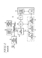
- the invention is implemented by circuitry shown in Figure 5 with optical disk controller (ODC) and optical data encoder-decoder (ODE) functions integrated on a common integrated circuit substrate.
- ODC optical disk controller
- ODE optical data encoder-decoder
- this invention can be practiced with separately provided ODC and ODE functions, using the architecture of Figure 2. Integration of functions in the manner shown in the preferred embodiment of Figure 5 is advantageous for reasons detailed in the copending "single chip" application.
- the integrated optical disk controller (IODC) 100 shown in Figure 5 comprises ODC and ODE regions 102, 104 that are depicted as being isolated in separate portions of the chip but in practice may be arranged differently based upon circuit layout constraints.
- the ODC 102 is similar to ODC 24 of the prior art, although programmed slightly differently and modified somewhat to accommodate new signals developed by the ODE 104.
- the ODE 104 has been modified considerably from the counterpart prior art unit 28. Aspects of IODC 100 implemented for data recovery are described in detail herein; more detail on other aspects of the IODC are provided in the single chip copending application.
- ODE 104 contains five principal functional circuits in addition to a FIFO and synchronization logic 108.
- Marks detection circuits 110, 112 detect the various byte patterns or marks forming reference points on the sectors taken from the tracks of an optical data disk being read.
- Mark detection and media control logic circuit 112 receives raw data (RAWDAT) taken from the disk, searches for the sector mark pattern provided by X3B11 specifications in the preferred embodiment, and supplies a sector mark found (SMF) signal to one input each of logic OR gates 113 and 115. To the other input of gate 113 is applied a psuedo sector mark signal developed by circuit 112, as described in the copending "sector mark” applications.
- the sector mark detection and media control logic circuit 112 is synchronized to an external constant reference clock (2FCLK) that operates at twice the frequency as that of ODC 102, that is, at the frequency of the RDREF clock, a requirement of NRZ/RLL 2,7 encoding and decoding.
- 2FCLK an external constant reference clock
- gate 113 The output of gate 113 in turn is supplied to an input of OR logic gate 114, the remaining input of which receives an address mark/sync found signal developed by circuit 110 when the corresponding reference marks read from the disk are detected.
- logic OR gate 115 receives the output of AND gate 111 whose inputs comprise the sector mark found signal (SMF) from circuit 112 and a user selected psuedo sector mark enable signal (PSME) from ODE registers 130 in ODC 102 as described in the "single chip" copending application.
- SMF sector mark found signal
- PSME psuedo sector mark enable signal
- Marks detection circuit 110 detects patterns of data taken from each sector to identify the presence of the address marks (AM), sync, resyncs (RS) and flag (flag detection is synchronized to 2FCLK). Flag pattern detection is described in detail in copending application Serial No. , entitled “Repetitive pattern Detection", also filed on even date herewith and incorporated herein by reference. Marks detection circuit 110 receives DATIN, which is a synchronized encoded data input received from an external phase locked loop (PLL), not shown in Figure 5 but corresponding to PLL 30 of Figure 2.
- PLL phase locked loop
- Address marks (AM) or sync found signals developed by marks detection circuit 110 are supplied to another input of logic OR gate 114 as well as to one input of logic OR gate 116. To the other input of gate 116 is provided a signal by marks detection circuit 110 indicating that a resync has been found.
- the output of logic OR gate 114 designating either that a sector mark, address mark or sync has been found, or a pseudo sector mark has been generated, is supplied to a data section 118 of ODC 102 to enable sector data to be aligned, stored and then transferred to a host bus.
- the output of gate 116 corresponding to address mark, sync or resync found, is supplied as an output MKF (marks found) signal for diagnostics.
- Window control logic circuit 120 controls the size of the resync detection window in accordance with an aspect of this invention.
- Other window sizes namely, those for detecting the sector mark, address mark, sync and flag are programmed in writable controls store (WCS) unit 122 of ODC data section 118.
- WCS writable controls store
- RLL decoder 124 receives DATIN from the disk, synchronized to SYNCLK, and converts the disk sector data from RLL 2,7 to NRZ data for supply to the FIFO and synchronization logic circuit 108.
- the circuit 108 synchronizes data read from the decoder 124 and marks read from circuit 110 to the reference clock obtained from divider block 125 by using a small FIFO (preferrably 2 bits wide by 14 bits deep). Data bit shift during resync detection is compensated by the FIFO.
- Block 108 also includes a counter for counting the length of the data segments and controlling generation of RDREF to the ODC 102 during resyncs. Data supplied by logic circuit 108 to data section 118 is read into the section only when RDREF is asserted. Details on this operation are given in the "single chip" copending application.
- RLL encoder and marks generation circuit 126 receives data from the data section 118, carries out RLL 2,7 encoding and generates various marks, such as sync, resyncs, etc., for each sector.
- Output signals at 128 and SMF at 127 are described in the copending "single chip” application.
- ODC 102 connected to the SCSI side of the controller, supplies data read and decoded from the disk by ODE 104 and synchronized to sync found signals provided by ODE 104 for storage in a buffer memory (not shown).
- Various status bits developed by ODE 104 are stored in ODE registers 130 of the ODC 102. As an example, if a sync is not matched, a status flag sill be set in register 130 with an optional interrupt, and a corresponding ID for that sector will be stored in an ODC register (not shown).
- a CPU (not shown) interfaced to ODC 102 will respond to the interrupt to scan the sector again or scan during the same pass through the sector in a data recovery mode of operation, described later in more detail.
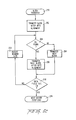
- Data read operation comprises two modes of operation.
- a "read header" routine 200 searches the header field for a pattern of bits corresponding to the sector mark using the sector mark algorithms described in the copending "sector mark” applications (step 202).
- the header is further searched in step 204 for finding an address mark (AM).
- ID identification
- CRC CRC data are read from the next field of the header (see Figure 4). This sequence is repeated until all identification fields are read (step 208).
- ID identification
- CRC data are read from the next field of the header (see Figure 4).
- This sequence is repeated until all identification fields are read (step 208).
- MO magnetooptic
- the data field is now searched, beginning with VFO 3.
- the search window is maintained wide open by WCS 122 until a sync is detected.
- the window is closed as shown in dotted lines in Figure 8-(b) and a sync found (SF) signal is developed by marks detection circuit 110 per step 214 (see Figure 8(c)).
- the program continues to a "block transfer" routine 250, shown in Figure 6(c), to byte align the sector data to resyncs distributed throughout the data field.
- the window remains open, as shown by the solid line in Figure 8(b), for a duration preset by the user and corresponding to the duration of the sector data field.
- the window is closed automatically based a previously programmed count J (step 216).
- a "no sync found" flag is stored in registers 130 of ODC 102 (step 220).
- the same routine can be carried out for successive sectors (step 222), or recovery of data for that sector can be provided using routine 230 shown in Figure 6(b) if the window size J of Figure 8(b) has been selected by the user to be small.
- the size of this small window is slightly greater than the length of the sync, as shown in Figure 8(d).
- the CPU responds to the "no sync found" flag. If data recovery is to be carried out in the same pass through the current sector, the interrupt is ignored. Otherwise, the header is again read (step 232) during a second pass through the sector by searching for the sync (step 234).
- the window used for searching for the sync during the second pass also has a fixed size, slightly greater than the length of the sync field, as shown in Figure 8(d).
- step 236 the ODE generates a pseudo sync signal (step 238), as shown in Figure 8(e), synchronized to the trailing edge of the window.
- the pseudo sync signal produced by the marks detection circuit 110, byte aligns the first block of sector data in the same manner as the sync found (SF) signal.
- the block transfer routine 250 transfers a first block of data (DS) (step 262) following byte alignment to the pseudo sync signal.
- a block of data (DS) may consist of, for example, 15 or 20 bytes, depending upon data format. If a resync (RS) byte is found (step 264), the next block (DS) is byte aligned and transferred, as provided in step 266. If RS is not found in step 264, the block (DS) is transferred without any byte alignment (268). The importance of this step is that the data, although not byte aligned, is not lost. It is supplied to error correction circuitry (not shown) that will be able to correct up to a particular number of data blocks.
- step 270 After checking the data field count in step 270, the routine returns to step 264 to search for the resync byte after adjusting window size in step 272, as described below.
- the size of the window is maintained fixed at the maximum. Thereafter, when a resync byte is found, the resync window size is reduced to a predetermined minimum, and progressively increased in size for successive resync bytes, as shown in Figure 7(c). Window size is increased progressively to the predetermined maximum (selected as a function of the length of the data section of each sector and the speed tolerence of the disk medium) controlled by window logic circuit 120. However, each time the resync byte is detected, the window size is reduced to the minimum, and the sequence repeats, as shown in Figure 7(c).
- the block transfer routine of Figure 6(c) operates in either of two modes, selected by the user.
- a first mode the size of the window is fixed for successive resync bytes as shown in Figure 7(b); in the other the size of the resync window increases progressively (e.g., from -3 to -12) as in Figure 7(c) and in the same manner as recovery mode.
- the invention described above accordingly carries out data recovery in the absence of a good sync mark in the disk data by forcing data to be read from a sector by aligning the first data block to a pseudo sync mark generated at the location of the sector when the sync mark is expected to reside.
- the bit stream is aligned to resyncs distributed in the data field of the sector.
- the size of the search window for finding successive resyncs is appropriately controlled for normal read and data recovery modes of operation based upon the probability that the next resync will be found in the expected region of the field.
Landscapes
- Engineering & Computer Science (AREA)
- Signal Processing (AREA)
- General Engineering & Computer Science (AREA)
- Signal Processing For Digital Recording And Reproducing (AREA)
- Optical Recording Or Reproduction (AREA)
Abstract
Description
- This invention relates generally to reading data from optical data disks, and more particularly to recovery of data from disk sectors having missing or defective synchronization marks.
- Optical disk media are capable of storing a considerable amount of data in the form of small marks or holes in the surface of the disk, each representing a bit of data. The marks, burned into the surface of the disk by a laser, are arranged along spiral tracks, each divided into a number of sectors.
- Figure 1 is a diagram of an
apparatus 10 for reading data prerecorded on anoptical disk 12. Thedisk 12 is rotated by adisk servo 14 comprising a precisely controllable DC motor. Alaser 16 irradiates the surface of thedisk 12, and light reflected from the disk impinges on the surface of adetector 18. Anoptical head 20, located between thedisk 12 and laser/detector laser 16 to form surface marks corresponding to data. The servos and laser/detector are controlled by aprocessor unit 22. - The
components comprising apparatus 10 shown in Figure 1 typically are arranged within a common housing, such as provided by SCSI (Small Computer System Interface) resident at a personal computer or other computer requiring storage of a large quantity of data. - Data read and write logic, implemented by
processor unit 22 in the representative illustration of Figure 1, has been carried out by commercially available special function integrated circuits, such as the AM95C96 optical disk controller (ODC), manufactured by Advanced Micro Devices of Sunnyvale, California. A system implementing the AM95C96, shown in Figure 2, comprisesODC 24 reading data through an encoder/decoder (ODE) 28 and a phase locked loop (PLL) 30 off the optical disk and writing to the optical disk. ACPU 32 controls seeking to the desired location on the disk. The ODC/ODE CPU 32,working memory 34 and adisk interface 36 to process the applied data signals and transfer commands for compliance with particular specifications such as the X3B11 continuous composite servo (CCS), WORM/ERASABLE optical format developed by ANSI. - The ODC 24 is interfaced to a system bus by
host interface unit 38, and is supported bybuffer memory 40 anderror processor 42. General operation of the system shown in Figure 2, being known to the prior art, is not described in detail. An improvement integrating the ODC/ODE - Figure 3 depicts the layout of tracks on an optical disk. The tracks are arranged along a spiral path on the surface of the
disk 12, with each turn of the spiral being treated as a separate track. In one example, the optical disk may be 90mm in diameter, and may contain 10,000 tracks (numbered 0-9999 in Figure 3); each track is divided into twenty-five (25) sectors. Each sector in turn will carry 725 bytes of unformatted data. The optical disk in this example is capable of storing 181,250,000 bytes of data, or about 100,000 pages of text. Modifications include implementing more densely packed sectors, larger diameter disks and/or double- sided storage for enhanced information storage capacity. - Figure 4 is a field diagram of the X3B11 format, comprising a header area that is "pre-stamped", followed by a data area for receiving data for storage. The first field of the header is a sector mark (SM) having a special redundant pattern. This field identifies the start of a sector. The SM field as well as the other fields constituting the X3B11 format is summarized below in Table I.
-

- During both reading and writing operations,
ODE 26 or the ODE section of the IODC described in the copending application, detects sector mark (SM) once within each sector. Referring to Table I, the sector mark comprises 80 bits arranged as a long burn followed by a transition pattern. Sector mark decoding is carried out by monitoring the long burn pattern of the track, and identifying a pattern characteristic of the sector mark. An algorithm for this purpose is described in my copending application S.N. entitled "Sector Mark Detection in Long Burn Pattern for Optical Data Disks," (hereinafter referred to as "sector mark copending applications"), filed concurrently herewith and incorporated by reference. - Detection of the sector mark pattern is a prerequisite to the reading of data from the corresponding sector. It identifies the region of each sector from which data is to be read because the data field is displaced from the sector mark by a defined number of bytes depending upon the particular standard involved. For example, in conventional X3B11 format, shown symbolically in Figure 4, the pre-stamped, or read only (RO), region extends 47 bytes beyond the sector mark field SM, followed by a magneto-optic region (MO) upon which data can be written once (the MO region is also termed a "WORM", or write once- read many, region). The data region of a 90mm, 512 byte sector size by convention follows the RO region by ODF and GAP bytes. The next sector mark field follows the data field by a buffer region of 13 bytes for timing margins.
- Another prerequisite of reading data from the disk is byte and bit alignment of data taken off each sector for decoding. In the X3B11 specification shown in Figure 4, a synchronization mark (hereinafter termed "sync") of 3 bytes, signifying the start of the sector data field, follows VF03. There are also several re-synchronization marks ("resyncs") of one byte each at regular intervals to ensure byte alignment throughout a read operation. Following a successful header operation, the VF03 field is searched for presence of the sync. Upon detection of the sync, a "sync found" signal is generated by the ODE and the incoming data stream is decoded one block at a time while data synchronization is maintained by alignment to the resyncs.
- In case of sync misdetection as a result of a defect in disk medium or dirt, the sector data will not be able to be read reliably because there is no synchronization of the data stream. Even if the sync is found, failure to detect resyncs will cause the data stream not to byte align properly throughout the read operation. Although a few misaligned blocks of data can be corrected, several misalignments may exceed the allowable data correction capability of available error correction circuitry. Searching for the resyncs using conventional windowing techniques tends to be inaccurate because the size of the search window does not always conform to the probability that a resync will be found.
- We describe a controller system which recovers sector data in the absence of a sync and aligns data to resyncs distributed in the data field of a sector. The system searches for resyncs by windowing in such a manner as to take into account the probability finding resyncs in the designated region of a sector.
- The recovery routine of this system enables data to be read from a designated sector of an optical data disk in the presence of damaged or missing syncs or resyncs. The optical data disk is of a type that stores data in sectors arranged serially along a multiplicity of tracks, with each sector having header and data fields preferably conforming to X3B11 specifications.
- The routine is carried out first by searching a selected sector of the data disk to detect a sync pattern of bits designating a portion of the data field from which sector data is to be aligned. If the sync pattern is found, a normal data read operation including byte alignment of a first block data from the sector data field is performed. If the sync pattern is not found, the selected sector is searched again and a data recovery operation is performed to "force" byte alignment of the first block of data. This sequence is repeated for any other designated sectors.
- In accordance with another aspect of the system, a "sync found" signal is generated upon finding the sync pattern of bits. If no sync pattern is found, a "pseudo sync" signal is generated. The first block of data is byte aligned to the "sync found" signal during normal read and to the "pseudo sync" signal during data recovery.
- In accordance with a further aspect, the data field is searched to find at least one resync pattern of bits designating another portion of the data field from which alignment of sector data is to be maintained. In normal data read operation, resync pattern searching is performed using either a search window of fixed size or a search window of varying size for successive resyncs. In data recovery operation, the search window for resyncs initially is set at a maximum size. Upon finding a resync, the window is reduced to a minimum size, and is then increased in size progressively for successive missing resyncs. When a resync is next found, the size of the window again is reduced to the minimum, and so on.
- In the accompanying drawings, by way of example only:-
- Figure 1 is a simplified diagram of an optical disk read/write system within which the present invention may be implemented.
- Figure 2 is a diagram of an optical disk controller system of the prior art.
- Figure 3 is a diagram showing a track format of an optical data disk.
- Figure 4 is a diagram showing X3B11 data format utilized in the preferred embodiment.
- Figure 5 is a block diagram of an optical disk controller incorporating data recovery in accordance with the invention.
- Figures 6(a)-(c) are flow charts for programming for carrying out aspects of the invention.
- Figures 7(a)-(c) are waveforms for describing the various search windows generated during data recovery.
- Figures 8(a)-(e) are waveforms for describing sync found and pseudo sync signal generation in during the data read and recovery modes of operation.
- Upon failure to find a sync while reading sector data from a track of an optical data disk, an optical data disk controller carries out data recovery, in accordance with the invention, to "forcibly read" data from the region of the sector where data is presumed to reside. The data taken from the sector is byte aligned to resync bytes at regular intervals of the data. Data blocks are supplied to error correction circuitry to correct for non-alignment errors and other errors in the bit stream.
- The invention is implemented by circuitry shown in Figure 5 with optical disk controller (ODC) and optical data encoder-decoder (ODE) functions integrated on a common integrated circuit substrate. Alternatively, this invention can be practiced with separately provided ODC and ODE functions, using the architecture of Figure 2. Integration of functions in the manner shown in the preferred embodiment of Figure 5 is advantageous for reasons detailed in the copending "single chip" application.
- The integrated optical disk controller (IODC) 100 shown in Figure 5 comprises ODC and
ODE regions ODC 102 is similar toODC 24 of the prior art, although programmed slightly differently and modified somewhat to accommodate new signals developed by theODE 104. TheODE 104 has been modified considerably from the counterpartprior art unit 28. Aspects ofIODC 100 implemented for data recovery are described in detail herein; more detail on other aspects of the IODC are provided in the single chip copending application. - Referring to Figure 5 in more detail,
ODE 104 contains five principal functional circuits in addition to a FIFO andsynchronization logic 108.Marks detection circuits 110, 112 detect the various byte patterns or marks forming reference points on the sectors taken from the tracks of an optical data disk being read. - Mark detection and media
control logic circuit 112 receives raw data (RAWDAT) taken from the disk, searches for the sector mark pattern provided by X3B11 specifications in the preferred embodiment, and supplies a sector mark found (SMF) signal to one input each of logic ORgates gate 113 is applied a psuedo sector mark signal developed bycircuit 112, as described in the copending "sector mark" applications. The sector mark detection and mediacontrol logic circuit 112 is synchronized to an external constant reference clock (2FCLK) that operates at twice the frequency as that ofODC 102, that is, at the frequency of the RDREF clock, a requirement of NRZ/RLL - The output of
gate 113 in turn is supplied to an input of ORlogic gate 114, the remaining input of which receives an address mark/sync found signal developed by circuit 110 when the corresponding reference marks read from the disk are detected. - The remaining input of logic OR
gate 115 receives the output of AND gate 111 whose inputs comprise the sector mark found signal (SMF) fromcircuit 112 and a user selected psuedo sector mark enable signal (PSME) fromODE registers 130 inODC 102 as described in the "single chip" copending application. - Marks detection circuit 110 detects patterns of data taken from each sector to identify the presence of the address marks (AM), sync, resyncs (RS) and flag (flag detection is synchronized to 2FCLK). Flag pattern detection is described in detail in copending application Serial No. , entitled "Repetitive pattern Detection", also filed on even date herewith and incorporated herein by reference. Marks detection circuit 110 receives DATIN, which is a synchronized encoded data input received from an external phase locked loop (PLL), not shown in Figure 5 but corresponding to
PLL 30 of Figure 2. This data containing RLL data as well as the AM, sync, resyncs and VFO patterns taken directly from the disk, is synchronized to a clock SYNCLK provided by the PLL. Also supplied to circuit 110 is flag data (FLGDAT) providing flag detection obtained from encoded disk data. - Address marks (AM) or sync found signals developed by marks detection circuit 110 are supplied to another input of logic OR
gate 114 as well as to one input of logic ORgate 116. To the other input ofgate 116 is provided a signal by marks detection circuit 110 indicating that a resync has been found. The output of logic ORgate 114, designating either that a sector mark, address mark or sync has been found, or a pseudo sector mark has been generated, is supplied to adata section 118 ofODC 102 to enable sector data to be aligned, stored and then transferred to a host bus. The output ofgate 116, corresponding to address mark, sync or resync found, is supplied as an output MKF (marks found) signal for diagnostics. - Window
control logic circuit 120 controls the size of the resync detection window in accordance with an aspect of this invention. Other window sizes, namely, those for detecting the sector mark, address mark, sync and flag are programmed in writable controls store (WCS)unit 122 ofODC data section 118. -
RLL decoder 124 receives DATIN from the disk, synchronized to SYNCLK, and converts the disk sector data fromRLL synchronization logic circuit 108. Thecircuit 108 synchronizes data read from thedecoder 124 and marks read from circuit 110 to the reference clock obtained fromdivider block 125 by using a small FIFO (preferrably 2 bits wide by 14 bits deep). Data bit shift during resync detection is compensated by the FIFO. Block 108 also includes a counter for counting the length of the data segments and controlling generation of RDREF to theODC 102 during resyncs. Data supplied bylogic circuit 108 todata section 118 is read into the section only when RDREF is asserted. Details on this operation are given in the "single chip" copending application. - RLL encoder and marks
generation circuit 126 receives data from thedata section 118, carries outRLL - Output signals at 128 and SMF at 127, provided principally for diagnostics, are described in the copending "single chip" application.
-
ODC 102, connected to the SCSI side of the controller, supplies data read and decoded from the disk byODE 104 and synchronized to sync found signals provided byODE 104 for storage in a buffer memory (not shown). Various status bits developed byODE 104 are stored in ODE registers 130 of theODC 102. As an example, if a sync is not matched, a status flag sill be set inregister 130 with an optional interrupt, and a corresponding ID for that sector will be stored in an ODC register (not shown). A CPU (not shown) interfaced toODC 102, will respond to the interrupt to scan the sector again or scan during the same pass through the sector in a data recovery mode of operation, described later in more detail. - Data read operation, in accordance with the invention, comprises two modes of operation. Referring to Figure 6(a), in the first mode of operation, a "read header" routine 200, searches the header field for a pattern of bits corresponding to the sector mark using the sector mark algorithms described in the copending "sector mark" applications (step 202). When a sector mark is found, the header is further searched in
step 204 for finding an address mark (AM). Assuming that the address mark is found, identification (ID) and CRC data are read from the next field of the header (see Figure 4). This sequence is repeated until all identification fields are read (step 208). In the XB311 specifications, there are three ID fields. Once all three fields are read bystep 208, the program advances to a "read data" routine (step 210), where data from the magnetooptic (MO) field is read from the disk. - The data field is now searched, beginning with
VFO 3. Referring to Figures 8(a) and 8(b), during the first pass through the Sector shown, the search window is maintained wide open byWCS 122 until a sync is detected. Upon detection of a sync,step 212, the window is closed as shown in dotted lines in Figure 8-(b) and a sync found (SF) signal is developed by marks detection circuit 110 per step 214 (see Figure 8(c)). The program continues to a "block transfer" routine 250, shown in Figure 6(c), to byte align the sector data to resyncs distributed throughout the data field. - Assuming, however, that a sync is not found in
step 212, the window remains open, as shown by the solid line in Figure 8(b), for a duration preset by the user and corresponding to the duration of the sector data field. The window is closed automatically based a previously programmed count J (step 216). When the count is reduced to zero, step 218, a "no sync found" flag is stored inregisters 130 of ODC 102 (step 220). The same routine can be carried out for successive sectors (step 222), or recovery of data for that sector can be provided using routine 230 shown in Figure 6(b) if the window size J of Figure 8(b) has been selected by the user to be small. The size of this small window is slightly greater than the length of the sync, as shown in Figure 8(d). - The CPU responds to the "no sync found" flag. If data recovery is to be carried out in the same pass through the current sector, the interrupt is ignored. Otherwise, the header is again read (step 232) during a second pass through the sector by searching for the sync (step 234). The window used for searching for the sync during the second pass also has a fixed size, slightly greater than the length of the sync field, as shown in Figure 8(d).
- There is a small possibility that the sync will be detected on the second pass. If so, the program returns to step 214, Figure 6(a), for generation of the sync found signal. However, ordinarily the sync will not be found during the second pass. Upon expiration of a timeout period presented by
WCS 122 and corresponding to the window shown in Figure 8(d),step 236, the ODE generates a pseudo sync signal (step 238), as shown in Figure 8(e), synchronized to the trailing edge of the window. The pseudo sync signal, produced by the marks detection circuit 110, byte aligns the first block of sector data in the same manner as the sync found (SF) signal. This is a "forced read" of sector data for byte alignment to resync (RS) bytes distributed uniformly in the data field. Because no sync has been found, however, the resync window initially is set to be wide open (step 240) and the program continues to the "block transfer"routine 250 of Figure 6(c). A wide-open resync window corresponds to a length of 12 2FCLK, when each resync (RS) consists of one byte for X3B11 specifications, as shown in Figures 7(a) and 7(b). - During recovery mode operation the window size initially is maintained fixed at a maximum size throughout the data field read until a resync is found. Accordingly, in Figure 6(c), the
block transfer routine 250 transfers a first block of data (DS) (step 262) following byte alignment to the pseudo sync signal. A block of data (DS) may consist of, for example, 15 or 20 bytes, depending upon data format. If a resync (RS) byte is found (step 264), the next block (DS) is byte aligned and transferred, as provided instep 266. If RS is not found instep 264, the block (DS) is transferred without any byte alignment (268). The importance of this step is that the data, although not byte aligned, is not lost. It is supplied to error correction circuitry (not shown) that will be able to correct up to a particular number of data blocks. - After checking the data field count in
step 270, the routine returns to step 264 to search for the resync byte after adjusting window size instep 272, as described below. - If a resync byte has not been found, the size of the window is maintained fixed at the maximum. Thereafter, when a resync byte is found, the resync window size is reduced to a predetermined minimum, and progressively increased in size for successive resync bytes, as shown in Figure 7(c). Window size is increased progressively to the predetermined maximum (selected as a function of the length of the data section of each sector and the speed tolerence of the disk medium) controlled by
window logic circuit 120. However, each time the resync byte is detected, the window size is reduced to the minimum, and the sequence repeats, as shown in Figure 7(c). - During normal data read, the block transfer routine of Figure 6(c) operates in either of two modes, selected by the user. In a first mode, the size of the window is fixed for successive resync bytes as shown in Figure 7(b); in the other the size of the resync window increases progressively (e.g., from -3 to -12) as in Figure 7(c) and in the same manner as recovery mode.
- The invention described above accordingly carries out data recovery in the absence of a good sync mark in the disk data by forcing data to be read from a sector by aligning the first data block to a pseudo sync mark generated at the location of the sector when the sync mark is expected to reside. The bit stream is aligned to resyncs distributed in the data field of the sector. The size of the search window for finding successive resyncs is appropriately controlled for normal read and data recovery modes of operation based upon the probability that the next resync will be found in the expected region of the field.
- In this disclosure, there is shown and described only the preferred embodiment of the invention, but, as aforementioned, it is to be understood that the invention is capable of use in various other combinations and environments and is capable of changes or modifications within the scope of the inventive concept as expressed herein.
Claims (22)
data is byte aligned respectively to said "sync found" and said "pseudo sync" signals during said normal data read and data recovery operations.
Applications Claiming Priority (2)
| Application Number | Priority Date | Filing Date | Title |
|---|---|---|---|
| US813272 | 1991-12-24 | ||
| US07/813,272 US5416760A (en) | 1991-12-16 | 1991-12-24 | Recovery of data from optical data disk sectors having missing or defective synchronization information |
Publications (2)
| Publication Number | Publication Date |
|---|---|
| EP0549151A2 true EP0549151A2 (en) | 1993-06-30 |
| EP0549151A3 EP0549151A3 (en) | 1993-12-01 |
Family
ID=25211942
Family Applications (1)
| Application Number | Title | Priority Date | Filing Date |
|---|---|---|---|
| EP19920310961 Withdrawn EP0549151A3 (en) | 1991-12-24 | 1992-12-01 | Optical data disk control systems |
Country Status (4)
| Country | Link |
|---|---|
| US (1) | US5416760A (en) |
| EP (1) | EP0549151A3 (en) |
| JP (1) | JPH05242611A (en) |
| KR (1) | KR930014371A (en) |
Cited By (21)
| Publication number | Priority date | Publication date | Assignee | Title |
|---|---|---|---|---|
| EP0634747A2 (en) * | 1993-07-14 | 1995-01-18 | Nec Corporation | Optical information control device and synchronizing method thereof |
| EP0680043A2 (en) * | 1994-04-26 | 1995-11-02 | Nec Corporation | Disc controller |
| EP1096491A1 (en) * | 1999-10-26 | 2001-05-02 | Iomega Corporation | Synchronization recovery technique for storage media |
| CN1073737C (en) * | 1995-09-06 | 2001-10-24 | 三星电子株式会社 | Sync. detecting and protecting circuit and method thereof |
| EP2360696A1 (en) * | 2010-02-24 | 2011-08-24 | LSI Corporation | Systems and methods for data recovery |
| US8516348B2 (en) | 2009-03-06 | 2013-08-20 | Agere Systems Inc. | Systems and methods for enhanced media defect detection |
| US8612843B2 (en) | 2011-08-19 | 2013-12-17 | Lsi Corporation | Systems and methods for qualitative media defect determination |
| US8675297B2 (en) | 2012-06-15 | 2014-03-18 | Lsi Corporation | Media defect classification |
| US8732562B2 (en) | 2012-07-25 | 2014-05-20 | Lsi Corporation | Systems and methods for improved short media defect detection |
| US8788921B2 (en) | 2011-10-27 | 2014-07-22 | Lsi Corporation | Detector with soft pruning |
| US8819521B2 (en) | 2012-04-30 | 2014-08-26 | Lsi Corporation | Systems and methods for short media defect detection using non-binary coded information |
| US8826110B2 (en) | 2012-07-17 | 2014-09-02 | Lsi Corporation | Systems and methods for defect scanning |
| US8843813B2 (en) | 2007-10-01 | 2014-09-23 | Agere Systems Inc | Systems and methods for media defect detection |
| US8917468B1 (en) | 2013-06-06 | 2014-12-23 | Lsi Corporation | Systems and methods for media defect detection with pattern qualification |
| US8949701B2 (en) | 2008-09-23 | 2015-02-03 | Agere Systems Inc. | Systems and methods for low latency media defect detection |
| US8972800B2 (en) | 2012-07-30 | 2015-03-03 | Lsi Corporation | Systems and methods for enhanced media defect detection |
| US8996970B2 (en) | 2012-10-24 | 2015-03-31 | Lsi Corporation | Systems and methods for positive feedback short media defect detection |
| US9076492B2 (en) | 2012-07-12 | 2015-07-07 | Lsi Corporation | Systems and methods for rapid erasure retry decoding |
| US9129653B2 (en) | 2012-04-20 | 2015-09-08 | Avago Technologies General Ip (Singapore) Pte. Ltd. | Systems and methods for calibration coasting in a data processing system |
| US9244752B2 (en) | 2013-05-02 | 2016-01-26 | Avago Technologies General Ip (Singapore) Pte. Ltd. | Systems and methods for detecting media flaws |
| US9245586B2 (en) | 2012-10-18 | 2016-01-26 | Avago Technologies General Ip (Singapore) Pte. Ltd. | Systems and methods for short media defect detection using multi-iteration soft data feedback |
Families Citing this family (17)
| Publication number | Priority date | Publication date | Assignee | Title |
|---|---|---|---|---|
| US5424881A (en) * | 1993-02-01 | 1995-06-13 | Cirrus Logic, Inc. | Synchronous read channel |
| USRE40996E1 (en) | 1993-03-15 | 2009-11-24 | Panasonic Corporation | Optical recording disk capable of resynchronization in digital encoding and decoding |
| JP2863052B2 (en) * | 1993-03-15 | 1999-03-03 | 松下電器産業株式会社 | Digital data encoding method, decoding method, encoding device, and decoding device |
| JP2916373B2 (en) * | 1994-06-02 | 1999-07-05 | オリンパス光学工業株式会社 | Information recording medium and information reproducing apparatus |
| KR100208380B1 (en) * | 1996-10-09 | 1999-07-15 | 윤종용 | A gray decoding compensation and its method of a hard disk drive |
| US5844920A (en) * | 1996-11-07 | 1998-12-01 | Cirrus Logic, Inc. | Thermal asperity compensation using multiple sync marks for retroactive and split segment data synchronization in a magnetic disk storage system |
| KR100528108B1 (en) * | 1996-11-22 | 2006-03-16 | 산요덴키가부시키가이샤 | Synchronization circuit and optical disc player for realizing high precision synchronization |
| JPH11273249A (en) * | 1998-03-20 | 1999-10-08 | Pioneer Electron Corp | Recording timing setting method, its device, information recording method, and its device |
| KR100362567B1 (en) | 1998-12-24 | 2003-04-07 | 삼성전자 주식회사 | Synchronous information detection method for decoding the information recorded in the burst cutting area |
| US6751037B1 (en) | 1999-06-24 | 2004-06-15 | Seagate Technology Llc | Audio-visual drive optimized for response to an undetected synchronization field |
| CN1359522A (en) * | 1999-06-24 | 2002-07-17 | 西加特技术有限责任公司 | Audio-visual disk drive optimized for response to an undatected synchronization field |
| US6463559B1 (en) | 1999-06-30 | 2002-10-08 | International Business Machines Corporation | Non-volatile fault indicator |
| US6694458B1 (en) * | 2000-09-07 | 2004-02-17 | Mosel Vitelic Corporation | Method and system for automatically validating a header search in reading data from an optical medium |
| GB0130208D0 (en) * | 2001-12-18 | 2002-02-06 | Nokia Corp | Synchronised window adaption |
| TW200535821A (en) * | 2004-04-30 | 2005-11-01 | Lite On It Corp | Method of inspecting disc information |
| US20070002126A1 (en) * | 2005-06-29 | 2007-01-04 | Lipinski Greg J | Preheating optical disc prior to optically writing to label area of optical disc |
| US8345369B2 (en) * | 2010-02-24 | 2013-01-01 | Lsi Corporation | Systems and methods for data recovery using enhanced sync mark location |
Citations (11)
| Publication number | Priority date | Publication date | Assignee | Title |
|---|---|---|---|---|
| JPS60145566A (en) * | 1984-01-05 | 1985-08-01 | Ricoh Co Ltd | Data recording and reproducing system |
| JPS60185260A (en) * | 1984-03-05 | 1985-09-20 | Ricoh Co Ltd | Digital signal recording system |
| JPS6126975A (en) * | 1984-07-17 | 1986-02-06 | Mitsubishi Electric Corp | Optical disk controller |
| US4641326A (en) * | 1983-10-14 | 1987-02-03 | Nippon Gakki Seizo Kabushiki Kaisha | Counter circuit operable in synchronism with frame or digital data signal |
| EP0236017A2 (en) * | 1986-02-27 | 1987-09-09 | Sony Corporation | Synchronizing signal decoding |
| US4879731A (en) * | 1988-08-24 | 1989-11-07 | Ampex Corporation | Apparatus and method for sync detection in digital data |
| EP0341852A2 (en) * | 1988-05-12 | 1989-11-15 | Quantum Corporation | High efficiency disk format and synchronization system |
| JPH01307062A (en) * | 1988-06-03 | 1989-12-12 | Olympus Optical Co Ltd | Data recording and reproducing device |
| US4908812A (en) * | 1985-09-13 | 1990-03-13 | Yamaha Corporation | Synchronizing signal reproducing circuit in a disc playback device |
| JPH02113469A (en) * | 1988-10-21 | 1990-04-25 | Daicel Chem Ind Ltd | Detector for optical disk synchronizing signal |
| EP0438355A1 (en) * | 1990-01-17 | 1991-07-24 | Fujitsu Limited | Method for reading a synchronizing signal from a record medium and an apparatus therefor |
Family Cites Families (10)
| Publication number | Priority date | Publication date | Assignee | Title |
|---|---|---|---|---|
| US4141046A (en) * | 1977-09-14 | 1979-02-20 | Exxon Research & Engineering Co. | Floppy disc data separator for use with single density encoding |
| JPS5753880A (en) * | 1980-09-12 | 1982-03-31 | Victor Co Of Japan Ltd | Detector of periodic signal |
| CA1212729A (en) * | 1981-12-08 | 1986-10-14 | Hiroshi Ogawa | Digital signal detecting and compensating circuit with adjustable window signal |
| US4791622A (en) * | 1983-09-19 | 1988-12-13 | Storage Technology Partners 11 | Optical data format employing resynchronizable data sectors |
| JPH0760574B2 (en) * | 1984-03-26 | 1995-06-28 | 株式会社日立製作所 | Sector start signal generation circuit for optical disk device |
| JPS62164276A (en) * | 1986-01-13 | 1987-07-20 | Matsushita Electric Ind Co Ltd | Information recording and reproducing device |
| US5138599A (en) * | 1988-11-21 | 1992-08-11 | Matsushita Electric Industrial Co., Ltd. | Information recording medium having dummy tracks and information recording and reproducing apparatus |
| US5047877A (en) * | 1989-06-09 | 1991-09-10 | Eastman Kodak Company | Windowing method of and apparatus for address mark detection |
| JP2534778B2 (en) * | 1989-09-26 | 1996-09-18 | 株式会社日立製作所 | Information recording / reproducing system and information recording / reproducing apparatus |
| JPH03116583A (en) * | 1989-09-29 | 1991-05-17 | Toshiba Corp | Optical disk device |
-
1991
- 1991-12-24 US US07/813,272 patent/US5416760A/en not_active Expired - Lifetime
-
1992
- 1992-12-01 EP EP19920310961 patent/EP0549151A3/en not_active Withdrawn
- 1992-12-18 JP JP4338827A patent/JPH05242611A/en not_active Withdrawn
- 1992-12-24 KR KR1019920025473A patent/KR930014371A/en not_active Application Discontinuation
Patent Citations (11)
| Publication number | Priority date | Publication date | Assignee | Title |
|---|---|---|---|---|
| US4641326A (en) * | 1983-10-14 | 1987-02-03 | Nippon Gakki Seizo Kabushiki Kaisha | Counter circuit operable in synchronism with frame or digital data signal |
| JPS60145566A (en) * | 1984-01-05 | 1985-08-01 | Ricoh Co Ltd | Data recording and reproducing system |
| JPS60185260A (en) * | 1984-03-05 | 1985-09-20 | Ricoh Co Ltd | Digital signal recording system |
| JPS6126975A (en) * | 1984-07-17 | 1986-02-06 | Mitsubishi Electric Corp | Optical disk controller |
| US4908812A (en) * | 1985-09-13 | 1990-03-13 | Yamaha Corporation | Synchronizing signal reproducing circuit in a disc playback device |
| EP0236017A2 (en) * | 1986-02-27 | 1987-09-09 | Sony Corporation | Synchronizing signal decoding |
| EP0341852A2 (en) * | 1988-05-12 | 1989-11-15 | Quantum Corporation | High efficiency disk format and synchronization system |
| JPH01307062A (en) * | 1988-06-03 | 1989-12-12 | Olympus Optical Co Ltd | Data recording and reproducing device |
| US4879731A (en) * | 1988-08-24 | 1989-11-07 | Ampex Corporation | Apparatus and method for sync detection in digital data |
| JPH02113469A (en) * | 1988-10-21 | 1990-04-25 | Daicel Chem Ind Ltd | Detector for optical disk synchronizing signal |
| EP0438355A1 (en) * | 1990-01-17 | 1991-07-24 | Fujitsu Limited | Method for reading a synchronizing signal from a record medium and an apparatus therefor |
Non-Patent Citations (5)
| Title |
|---|
| PATENT ABSTRACTS OF JAPAN vol. 009, no. 320 (P-413) <2043> 14 December 1985 & JP 60 145566 A (RICOH KK) 01 August 1985 * |
| PATENT ABSTRACTS OF JAPAN vol. 010, no. 038 (P-428) <2095> 14 February 1986 & JP 60 185260 A (RICOH KK) 20 September 1985 * |
| PATENT ABSTRACTS OF JAPAN vol. 010, no. 180 (P-471) 24 June 1986 & JP 61 026975 A (MITSUBISHI ELECTRIC CORP.) 06 February 1986 * |
| PATENT ABSTRACTS OF JAPAN vol. 014, no. 104 (P-1013) 26 February 1990 & JP 01 307062 A (OLYMPUS OPTICAL CO. LTD) 12 December 1989 * |
| PATENT ABSTRACTS OF JAPAN vol. 014, no. 333 (P-1078) 18 July 1990 & JP 02 113469 A (DAICEL CHEM. IND. LTD) 25 April 1990 * |
Cited By (24)
| Publication number | Priority date | Publication date | Assignee | Title |
|---|---|---|---|---|
| EP0634747A2 (en) * | 1993-07-14 | 1995-01-18 | Nec Corporation | Optical information control device and synchronizing method thereof |
| EP0634747A3 (en) * | 1993-07-14 | 1998-01-28 | Nec Corporation | Optical information control device and synchronizing method thereof |
| EP0680043A2 (en) * | 1994-04-26 | 1995-11-02 | Nec Corporation | Disc controller |
| EP0680043A3 (en) * | 1994-04-26 | 1999-04-28 | Nec Corporation | Disc controller |
| CN1073737C (en) * | 1995-09-06 | 2001-10-24 | 三星电子株式会社 | Sync. detecting and protecting circuit and method thereof |
| EP1096491A1 (en) * | 1999-10-26 | 2001-05-02 | Iomega Corporation | Synchronization recovery technique for storage media |
| US6557113B1 (en) | 1999-10-26 | 2003-04-29 | Iomega Corporation | Synchronization recovery technique for storage media |
| US8843813B2 (en) | 2007-10-01 | 2014-09-23 | Agere Systems Inc | Systems and methods for media defect detection |
| US8949701B2 (en) | 2008-09-23 | 2015-02-03 | Agere Systems Inc. | Systems and methods for low latency media defect detection |
| US8516348B2 (en) | 2009-03-06 | 2013-08-20 | Agere Systems Inc. | Systems and methods for enhanced media defect detection |
| EP2360696A1 (en) * | 2010-02-24 | 2011-08-24 | LSI Corporation | Systems and methods for data recovery |
| US8612843B2 (en) | 2011-08-19 | 2013-12-17 | Lsi Corporation | Systems and methods for qualitative media defect determination |
| US8788921B2 (en) | 2011-10-27 | 2014-07-22 | Lsi Corporation | Detector with soft pruning |
| US9129653B2 (en) | 2012-04-20 | 2015-09-08 | Avago Technologies General Ip (Singapore) Pte. Ltd. | Systems and methods for calibration coasting in a data processing system |
| US8819521B2 (en) | 2012-04-30 | 2014-08-26 | Lsi Corporation | Systems and methods for short media defect detection using non-binary coded information |
| US8675297B2 (en) | 2012-06-15 | 2014-03-18 | Lsi Corporation | Media defect classification |
| US9076492B2 (en) | 2012-07-12 | 2015-07-07 | Lsi Corporation | Systems and methods for rapid erasure retry decoding |
| US8826110B2 (en) | 2012-07-17 | 2014-09-02 | Lsi Corporation | Systems and methods for defect scanning |
| US8732562B2 (en) | 2012-07-25 | 2014-05-20 | Lsi Corporation | Systems and methods for improved short media defect detection |
| US8972800B2 (en) | 2012-07-30 | 2015-03-03 | Lsi Corporation | Systems and methods for enhanced media defect detection |
| US9245586B2 (en) | 2012-10-18 | 2016-01-26 | Avago Technologies General Ip (Singapore) Pte. Ltd. | Systems and methods for short media defect detection using multi-iteration soft data feedback |
| US8996970B2 (en) | 2012-10-24 | 2015-03-31 | Lsi Corporation | Systems and methods for positive feedback short media defect detection |
| US9244752B2 (en) | 2013-05-02 | 2016-01-26 | Avago Technologies General Ip (Singapore) Pte. Ltd. | Systems and methods for detecting media flaws |
| US8917468B1 (en) | 2013-06-06 | 2014-12-23 | Lsi Corporation | Systems and methods for media defect detection with pattern qualification |
Also Published As
| Publication number | Publication date |
|---|---|
| US5416760A (en) | 1995-05-16 |
| KR930014371A (en) | 1993-07-23 |
| EP0549151A3 (en) | 1993-12-01 |
| JPH05242611A (en) | 1993-09-21 |
Similar Documents
| Publication | Publication Date | Title |
|---|---|---|
| EP0549151A2 (en) | Optical data disk control systems | |
| US5231545A (en) | Fault tolerant rll data sector address mark decoder | |
| US7057987B2 (en) | Optical disc apparatus | |
| US5508985A (en) | Method for detecting and processing synchronization marks extracted from a prerecorded wobbled groove on a compact disk | |
| US7099246B2 (en) | Method and apparatus for recording data on an optical disc with restarting writing of data after data recording interruption | |
| JP2662491B2 (en) | Servo mark pattern generation and detection method | |
| US5559983A (en) | Single chip controller for optical data disk drives | |
| US6671114B2 (en) | Method and apparatus for forming data sector suitable for high density hard disk drive | |
| US5351231A (en) | Programmable mark detection and windowing for optical disk controllers | |
| US5737371A (en) | Realignment of data stream from an optical disk | |
| US5237552A (en) | Sector mark detection in long burn pattern for optical data disks | |
| US5444685A (en) | Sector mark pattern detection for optical data disk controller | |
| EP0630018B1 (en) | Interblock gap detection in a data storage system | |
| EP0549153B1 (en) | Sector mark detection for optical data disks | |
| EP0549154A2 (en) | Repetitive pattern detection | |
| KR100403289B1 (en) | Magnetic disk separately having defect occurrence information in servo area and magnetic disk device for detecting the same | |
| EP0549155A2 (en) | Optical data disk control system | |
| JPS63173274A (en) | Data recording system | |
| JPS5994246A (en) | Optical disk device | |
| JPS5994244A (en) | Optical disk device | |
| JPH0770162B2 (en) | Optical information recording / reproducing method | |
| JPH05159478A (en) | Optical recording and reproducing device | |
| JP2000285614A (en) | Test device and test method for decoder | |
| JPH0652634A (en) | Clock signal generating device |
Legal Events
| Date | Code | Title | Description |
|---|---|---|---|
| PUAI | Public reference made under article 153(3) epc to a published international application that has entered the european phase |
Free format text: ORIGINAL CODE: 0009012 |
|
| AK | Designated contracting states |
Kind code of ref document: A2 Designated state(s): AT BE CH DE DK ES FR GB GR IE IT LI LU NL PT SE |
|
| PUAL | Search report despatched |
Free format text: ORIGINAL CODE: 0009013 |
|
| AK | Designated contracting states |
Kind code of ref document: A3 Designated state(s): AT BE CH DE DK ES FR GB GR IE IT LI LU NL PT SE |
|
| 17P | Request for examination filed |
Effective date: 19940513 |
|
| 17Q | First examination report despatched |
Effective date: 19951228 |
|
| GRAG | Despatch of communication of intention to grant |
Free format text: ORIGINAL CODE: EPIDOS AGRA |
|
| GRAG | Despatch of communication of intention to grant |
Free format text: ORIGINAL CODE: EPIDOS AGRA |
|
| GRAH | Despatch of communication of intention to grant a patent |
Free format text: ORIGINAL CODE: EPIDOS IGRA |
|
| STAA | Information on the status of an ep patent application or granted ep patent |
Free format text: STATUS: THE APPLICATION IS DEEMED TO BE WITHDRAWN |
|
| 18D | Application deemed to be withdrawn |
Effective date: 19980609 |