EP0545461A2 - Clock recovery circuit - Google Patents
Clock recovery circuit Download PDFInfo
- Publication number
- EP0545461A2 EP0545461A2 EP92203542A EP92203542A EP0545461A2 EP 0545461 A2 EP0545461 A2 EP 0545461A2 EP 92203542 A EP92203542 A EP 92203542A EP 92203542 A EP92203542 A EP 92203542A EP 0545461 A2 EP0545461 A2 EP 0545461A2
- Authority
- EP
- European Patent Office
- Prior art keywords
- data signal
- signal
- filter
- decided
- gate
- Prior art date
- Legal status (The legal status is an assumption and is not a legal conclusion. Google has not performed a legal analysis and makes no representation as to the accuracy of the status listed.)
- Granted
Links
Images

Classifications
-
- H—ELECTRICITY
- H04—ELECTRIC COMMUNICATION TECHNIQUE
- H04B—TRANSMISSION
- H04B1/00—Details of transmission systems, not covered by a single one of groups H04B3/00 - H04B13/00; Details of transmission systems not characterised by the medium used for transmission
- H04B1/69—Spread spectrum techniques
- H04B1/707—Spread spectrum techniques using direct sequence modulation
- H04B1/7073—Synchronisation aspects
- H04B1/7085—Synchronisation aspects using a code tracking loop, e.g. a delay-locked loop
-
- H—ELECTRICITY
- H04—ELECTRIC COMMUNICATION TECHNIQUE
- H04B—TRANSMISSION
- H04B1/00—Details of transmission systems, not covered by a single one of groups H04B3/00 - H04B13/00; Details of transmission systems not characterised by the medium used for transmission
- H04B1/69—Spread spectrum techniques
- H04B1/707—Spread spectrum techniques using direct sequence modulation
- H04B1/709—Correlator structure
Definitions
- the invention relates to a device for recovering a clock signal from a data signal with a data decoder clocked with the clock signal for obtaining a decided data signal from the data signal and with a voltage-controlled oscillator with an upstream loop filter for obtaining the clock signal from a control signal that can be derived from the data signal and the decided data signal .
- the invention further relates to a transmission system and a receiver with such a device.
- Devices of this type are required in receivers of digital message transmission systems in order to sample a transmitted data signal in the receiver with a clock signal.
- a device of the type mentioned is known.
- a received data signal is fed to a decision device and a delay / subtraction device, at whose output the difference signal is the difference between the data signal and a data signal delayed by one bit.
- the decision device is also supplied with the output signal of a voltage-controlled oscillator with an upstream loop filter as a clock signal.
- a signal obtained from the multiplication of the decided data signal and the difference signal is fed to the loop filter.
- the invention has for its object to provide a device of the type mentioned that simple Can be integrated in a manner that is also suitable for high frequencies.
- This object is achieved in a device of the type mentioned in the introduction that a DLL (delay-locked loop) correlation device is provided to obtain the control signal.
- a DLL delay-locked loop
- DLL correlation devices are used for the synchronization of code sequences and are, for example, from "Spread Spectrum Systems", p. 210 ff from RC Dixon, New York 1976 or from “The Delay-Locked Loop in Spread Spectrum Transmission: Analysis and Optimization ", selected work on communication systems No. 67, HW Schüssler, Er Weg known in 1988.
- a first input of the correlation device receives the data signal and a second input the output signal of the data decider, i.e. the decided data signal is fed.
- the clock signal is automatically set without adjustment or readjustment being necessary. This eliminates the need for time-consuming adjustment during the manufacture of the device.
- the device can be easily integrated with little effort.
- a correlation device which can be implemented in a cost-effective manner with gates, in particular EX-OR gates for correlation, is designed as a DLL delay correlator with two correlators, in each of which the data signal or the data signal delayed by a predefinable bit duration with the decided data signal or the decided one delayed by a predefinable bit duration Data signal is correlated, a difference generator being provided to obtain the control signal, which forms the control signal from the difference of signals at the output of the correlators.
- the data signal in two branches is correlated directly or time-shifted with the decided data signal directly or time-shifted.
- the predeterminable bit duration for the delay can be a multiple or even a fraction of the bit duration of the data signal.
- a generalized form of a DLL correlation device results if the correlation device is designed as a filter correlator with a first and a second filter, the data filter being able to be supplied to the first filter and the decided data signal being able to be supplied to the second filter, and the output signals of the filters being correlated with one another and the loop filter are fed.
- filter correlators are also selected from the code synchronization, for example from "Correlators with Analog Filter Pairs and Synthesis of Suitable Coding Signals for the Delay-Locked Loop", selected works on message systems No. 42, H.W. Schüssler, Er Weg known in 1980. This specifies conditions that lead to odd control characteristics.
- the data filter is supplied to the first filter in the correlation devices for clock synchronization and the decided data signal to the second filter.
- Square wave signals can be easily generated from the data signal are generated in that the data signal is fed to the correlation device via a limiter.
- a correlation device which can also be implemented in a simple manner has a first and a second EX-OR gate, the first EX-OR gate having the received data signal and the decided data signal and the second EX-OR gate a data signal delayed by one bit duration and the received data signal can be supplied and wherein the control signal is formed from the difference between the output signal of the first EX-OR gate and the output signal of the second EX-OR gate.
- the transmission system shown in FIG. 1 a consists of a transmitter 100, a receiver 101 and a transmission channel 103 through which the transmitter 100 and the receiver 101 are coupled to one another.
- a data signal 102 to be transmitted At the output of the transmitter 100 is a data signal 102 to be transmitted, which is supplied to the transmitter 101 via the transmission channel 103, so that a received data signal 104 is present at the input of the transmitter 101.
- the receiver 101 shown in FIG. 1a has a device for recovering a clock signal from the data signal 104, the function of which is explained in detail in connection with the following figures.
- reference character d is used for the received data signal designated by reference character 104 in FIG. 1a.
- FIG. 1b shows the basic arrangement of a device for clock recovery, which is based on a correlative method.
- a data signal d is fed to both a correlation device 14 and a data decider 11.
- a decided data signal e is also fed to the correlation device 14.
- a correlation signal k which controls a downstream voltage-controlled oscillator 12 via a loop filter 13.
- the voltage-controlled oscillator supplies a clock signal t for the data decider 11.
- a correlation takes place in the correlation device 14 the received data signal with the decided data signal e.
- the correlation signal k thus serves as an error signal for the retuning of the voltage-controlled oscillator.
- the received data signal d is thus correlated with the received data signal e, ie with an estimated value of the same data signal.
- Such a device for clock recovery has self-adjusting properties, since the regenerated clock signal is derived directly from the clock of the data signal d. As a result, the sampling phase is automatically updated in the data decider 11, so that complex adjustments and readjustments of the device are not required.
- FIG. 2 shows the basic illustration of a correlation device 14 which can be used for a device for clock recovery in accordance with the exemplary embodiment shown in FIG. 1.
- a received data signal d and a decided data signal e are fed to the correlation device 14.
- a control signal k is present at the output of the correlation device 14.
- the data signal d is fed to a first correlator K1 and a second correlator K2.
- the decided data signal e is likewise first fed to a second delay device 17b.
- the output signals of the delay devices 17a, 17b are forwarded to the correlators K1, K2.
- the correlators K1, K2 each consist of a multiplier and a downstream low-pass filter.
- the control signal k is present as the output signal k of the correlation device 14 as the difference signal.
- the correlation device shown in FIG. 2 is as DLL delay correlator designed.
- the received data signal d is correlated in two branches in the correlators K1, K2 directly or with a time shift with the decided data signal e directly or with a time shift.
- the difference between the output signals k1, k2 of the two correlators K1, K2 results in a superposition, so that finally a control signal k for controlling the voltage-controlled oscillator can be obtained.
- Such delay correlators can be implemented with gates, in particular EX-OR gates, with little effort, as is shown in FIG. 4a.
- FIG. 3 shows a further exemplary embodiment of a correlation device 14.
- the correlation device 14 is designed as a filter correlator with a first filter H1 and a second filter H2.
- the first filter H1 is supplied with the data signal d, the second filter H2 with the decided data signal e.
- a respectively filtered data signal h1 or decided data signal h2 is located at the output of the first H1 and the second H2 filter. Rules for these filters are "Correlators with Analog Filter Pairs and Synthesis of Appropriate Coding Signals for the Delay-Locked Loop", selected work on messaging systems No. 42, H.W. Schüssler, Er Weg, 1980 removable.
- the filtered signals h1, h2 are correlated with one another by means of a multiplier and a subsequent low-pass filtering. At the output of the low pass is the control signal k, which can be fed to the loop filter shown in FIG. 1.
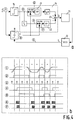
- FIG. 4a shows an exemplary embodiment of a device for clock recovery.
- a received data signal d is transmitted on the one hand via a limiter 15 of a correlation device 14 and on the other hand supplied to a data decider 11.
- a control signal k which controls a voltage-controlled oscillator 12 via a loop filter 13.
- the output signal of the voltage-controlled oscillator forms the clock signal t for clocking the data decider 11.
- a decided data signal e which is fed to the correlation device 14.
- the correlation device 14 consists of a first correlator 21 with an EX-OR gate and a downstream low-pass filter.
- the limited data signal and the decided data signal e are fed to the EX-OR gate.
- Correlation device 14 also has a second correlator 22 with a further EX-OR gate and a downstream low-pass filter.
- the EX-OR gate of the second correlator 22 is supplied with the data signal d delayed and limited by a bit duration Tb and the decided data signal e.
- the output signal of the first correlator 21 is delayed by half a bit duration and linked to the output signal of the second correlator 22 by forming a difference.
- the delay by half a bit duration T b / 2 can also be provided directly between the EX-OR gate and the low-pass filter of the first correlator 21. 4b, the signal curve for this embodiment is shown in track 6.
- FIG. 4b shows signal profiles of the device for clock recovery shown in FIG. 4a.
- the reference symbols surrounded by a circle in FIG. 4a correspond to the reference symbols used in FIG. 4b for identifying the signal profiles in tracks 1 to 7 also surrounded by a circle.
- Track 1 of the one shown in FIG. 4b shows an exemplary temporal course of the data signal d supplemented with the corresponding assignable logical values 1 or 0.
- Track 2 shows the output signal of the limiter shown in FIG. 4a.
- Track 3 shows the output signal of the voltage-controlled oscillator 12, ie the clock signal t formed from pulses, which marks the sampling times of the data decision maker.
- Track 4 shows the decided data signal e at the output of the data decider 11, which results from the received data signal d (track 1) by scanning with the clock or scan signal t shown in track 3.
- Track 5 shows the data signal delayed and limited by a bit duration Tb.
- Track 6 shows the output signal of the first correlator 21 delayed by half a bit duration, which is obtained from the limited data signal (track 2) and the received data signal e (track 4) by EX-OR operation.
- the time area is shown hatched, which is determined in the low-pass filtering, and the time area is shown cross-hatched, which results from the phase fluctuation of the data signal d shown in track 1.
- Track 7 finally shows the output signal of the second correlator 22, which is formed from an Ex-OR combination of the signal shown in track 5 and the received data signal (track 4).
- the time area that is determined in the low-pass filtering is also shown hatched in the signal shown in track 7, and the time area that is caused by phase fluctuations of the data signal shown in track 1 is shown cross-hatched.
- the delay by T b / 2 after the correlator 21 minimizes the interference AC voltage caused by the difference 23.
- Fig. 4a Based on the time profiles shown in Fig. 4b it is illustrated that with the help of those described in Fig. 4a Device for clock acquisition phase errors of the data signal can be compensated up to a maximum of plus / minus half a bit duration, ie the control range corresponds to 1T b . It is essential that in both signals of the track 6 and the track 7 supplied to the difference former 23, an opposite change in the mean value is taken into account. There is thus an automatic adjustment of the sampling phase of the clock signal t (track 3) without the need for a sampling phase adjustment or readjustment.
- the delay correlator shown in FIG. 4a can also be implemented in a simple manner in an integrated form.
Landscapes
- Engineering & Computer Science (AREA)
- Computer Networks & Wireless Communication (AREA)
- Signal Processing (AREA)
- Synchronisation In Digital Transmission Systems (AREA)
- Stabilization Of Oscillater, Synchronisation, Frequency Synthesizers (AREA)
Abstract
Description
Die Erfindung betrifft eine Einrichtung zur Rückgewinnung eines Taktsignals aus einem Datensignal mit einem mit dem Taktsignal getakteten Datenentscheider zur Gewinnung eines entschiedenen Datensignals aus dem Datensignal und mit einem spannungsgesteuerten Oszillator mit vorgeschaltetem Schleifenfilter zur Gewinnung des Taktsignals aus einem aus dem Datensignal und dem entschiedenen Datensignal ableitbaren Regelsignal.The invention relates to a device for recovering a clock signal from a data signal with a data decoder clocked with the clock signal for obtaining a decided data signal from the data signal and with a voltage-controlled oscillator with an upstream loop filter for obtaining the clock signal from a control signal that can be derived from the data signal and the decided data signal .
Die Erfindung betrifft weiter ein Übertragungssystem sowie einen Empfänger mit einer derartigen Einrichtung.The invention further relates to a transmission system and a receiver with such a device.
Derartige Einrichtungen werden in Empfängern von digitalen Nachrichtenübertragungssystemen benötigt, um ein übertragenes Datensignal im Empfänger mit einem Taktsignal abzutasten.Devices of this type are required in receivers of digital message transmission systems in order to sample a transmitted data signal in the receiver with a clock signal.
Aus US 4 423 518 ist eine Einrichtung der eingangs genannten Art bekannt. Dabei wird ein empfangenes Datensignal einer Entscheidungseinrichtung sowie einer Verzögerungs/Subtraktionseinrichtung zugeführt, an deren Ausgang als Differenzsignal die Differenz des Datensignals und eines um eine Bitdauer verzögerten Datensignals liegt. Der Entscheidungseinrichtung wird außerdem als Taktsignal das Ausgangssignal eines spannungsgesteuerten Oszillators mit vorgeschaltetem Schleifenfilter zugeführt. Ein aus der Multiplikation des entschiedenen Datensignals und des Differenzsignals gewonnenes Signal wird dem Schleifenfilter zugeführt.From US 4,423,518 a device of the type mentioned is known. In this case, a received data signal is fed to a decision device and a delay / subtraction device, at whose output the difference signal is the difference between the data signal and a data signal delayed by one bit. The decision device is also supplied with the output signal of a voltage-controlled oscillator with an upstream loop filter as a clock signal. A signal obtained from the multiplication of the decided data signal and the difference signal is fed to the loop filter.
Der Erfindung liegt die Aufgabe zugrunde, eine Einrichtung der eingangs genannten Art anzugeben, die auf einfache Weise integrierbar ist und die auch für hohe Frequenzen geeignet ist.The invention has for its object to provide a device of the type mentioned that simple Can be integrated in a manner that is also suitable for high frequencies.
Diese Aufgabe wird bei einer Einrichtung der eingangs genannten Art dadurch gelöst, daß zur Gewinnung des Regelsignals eine DLL (Delay-Locked-Loop)-Korrelationseinrichtung vorgesehen ist.This object is achieved in a device of the type mentioned in the introduction that a DLL (delay-locked loop) correlation device is provided to obtain the control signal.
DLL-Korrelationseinrichtungen werden zur Synchronisation von Codefolgen benutzt und sind beispielsweise aus "Spread Spectrum Systems", S. 210 ff von R. C. Dixon, New York 1976 oder aus "Der Delay-Locked-Loop in der Spread-Spectrum-Übertragung: Analyse und Optimierung", ausgewählte Arbeiten über Nachrichtensysteme Nr. 67, H.W. Schüssler, Erlangen 1988 bekannt. Im Gegensatz zu den aus der Codesynchronisation bekannten DLL-Korrelationseinrichtungen wird bei der Einrichtung zur Rückgewinnung des Taktsignals einem ersten Eingang der Korrelationseinrichtung das Datensignal sowie einem zweiten Eingang das Ausgangssignal des Datenentscheiders, d.h. das entschiedene Datensignal zugeführt. Hierdurch erfolgt eine selbsttätige Einstellung des Taktsignals, ohne daß eine Ein- bzw. Nachjustierung notwendig ist. Hierdurch entfällt ein aufwendiger Abgleich bei der Fertigung der Einrichtung. Darüber hinaus ist die Einrichtung bei geringem Aufwand leicht integrierbar.DLL correlation devices are used for the synchronization of code sequences and are, for example, from "Spread Spectrum Systems", p. 210 ff from RC Dixon, New York 1976 or from "The Delay-Locked Loop in Spread Spectrum Transmission: Analysis and Optimization ", selected work on communication systems No. 67, HW Schüssler, Erlangen known in 1988. In contrast to the DLL correlation devices known from code synchronization, in the device for recovering the clock signal, a first input of the correlation device receives the data signal and a second input the output signal of the data decider, i.e. the decided data signal is fed. As a result, the clock signal is automatically set without adjustment or readjustment being necessary. This eliminates the need for time-consuming adjustment during the manufacture of the device. In addition, the device can be easily integrated with little effort.
Eine mit Gattern, insbesondere EX-OR-Gattern zur Korrelation aufwandsgünstig realisierbare Korrelationseinrichtung ist als DLL-Verzögerungskorrelator mit zwei Korrelatoren ausgebildet, in denen jeweils das Datensignal oder das um eine vorgebbare Bitdauer verzögerte Datensignal mit dem entschiedenen Datensignal oder dem um eine vorgebbare Bitdauer verzögerten entschiedenen Datensignal korreliert wird, wobei zur Gewinnung des Regelsignals ein Differenzbildner vorgesehen ist, der aus der Differenz von Signalen am Ausgang der Korrelatoren das Regelsignal bildet. Hierbei wird im Gegensatz zu den aus der Codefolgensynchronisation bekannten DLL-Verzögerungskorrelatoren, bei denen eine Empfangsfolge in zwei Zweigen jeweils mit zeitverschobenen lokal erzeugten gleichen Codefolgen korreliert wird, das Datensignal in zwei Zweigen jeweils direkt oder zeitverschoben mit dem entschiedenen Datensignal direkt oder zeitverschoben korreliert. Die vorgebbare Bitdauer zur Verzögerung kann dabei ein Vielfaches oder auch nur einen Bruchteil der Bitdauer des Datensignals betragen. Durch die Differenzbildung der Ausgangssignale der beiden Korrelatoren erfolgt eine Überlagerung, so daß schließlich das Regelsignal zur Regelung des spannungsgesteuerten Oszillators gewinnbar ist.A correlation device which can be implemented in a cost-effective manner with gates, in particular EX-OR gates for correlation, is designed as a DLL delay correlator with two correlators, in each of which the data signal or the data signal delayed by a predefinable bit duration with the decided data signal or the decided one delayed by a predefinable bit duration Data signal is correlated, a difference generator being provided to obtain the control signal, which forms the control signal from the difference of signals at the output of the correlators. Here In contrast to the DLL delay correlators known from code sequence synchronization, in which a reception sequence in two branches is correlated with time-shifted locally generated same code sequences, the data signal in two branches is correlated directly or time-shifted with the decided data signal directly or time-shifted. The predeterminable bit duration for the delay can be a multiple or even a fraction of the bit duration of the data signal. The difference between the output signals of the two correlators is superimposed so that the control signal for controlling the voltage-controlled oscillator can finally be obtained.
Eine verallgemeinerte Form einer DLL-Korrelationseinrichtung ergibt sich, wenn die Korrelationseinrichtung als Filterkorrelator mit einem ersten und zweiten Filter ausgebildet wird, wobei dem ersten Filter das Datensignal und dem zweiten Filter das entschiedene Datensignal zuführbar ist und wobei die Ausgangssignale der Filter miteinander korreliert und dem Schleifenfilter zugeführt werden. Derartige Filterkorrelatoren sind ebenfalls aus der Codesynchronisation beispielsweise aus "Korrelatoren mit analogen Filterpaaren und Synthese geeigneter Codierungssignale für den Delay-Locked-Loop", ausgewählte Arbeiten über Nachrichtensysteme Nr. 42, H.W. Schüssler, Erlangen 1980 bekannt. Hierin sind Bedingungen angegeben, die auf ungerade Regelkennlinien führen. Im Gegensatz zu den hieraus bekannten Filterkorrelatoren, bei denen einem ersten Filter eine Empfangsfolge und einem zweiten Filter eine lokal erzeugte gleiche Codefolge zugeführt wird, wird bei den Korrelationseinrichtungen zur Taktsynchronisation dem ersten Filter das Datensignal und dem zweiten Filter das entschiedene Datensignal zugeführt.A generalized form of a DLL correlation device results if the correlation device is designed as a filter correlator with a first and a second filter, the data filter being able to be supplied to the first filter and the decided data signal being able to be supplied to the second filter, and the output signals of the filters being correlated with one another and the loop filter are fed. Such filter correlators are also selected from the code synchronization, for example from "Correlators with Analog Filter Pairs and Synthesis of Suitable Coding Signals for the Delay-Locked Loop", selected works on message systems No. 42, H.W. Schüssler, Erlangen known in 1980. This specifies conditions that lead to odd control characteristics. In contrast to the filter correlators known from this, in which a reception sequence is supplied to a first filter and a locally generated same code sequence is supplied to a second filter, the data filter is supplied to the first filter in the correlation devices for clock synchronization and the decided data signal to the second filter.
Aus dem Datensignal können auf einfache Weise Rechtecksignale dadurch erzeugt werden, daß das Datensignal der Korrelationseinrichtung über einen Begrenzer zugeführt wird.Square wave signals can be easily generated from the data signal are generated in that the data signal is fed to the correlation device via a limiter.
Eine auf einfache Weise auch integriert realisierbare Korrelationseinrichtung weist ein erstes und ein zweites EX-OR-Gatter auf, wobei dem ersten EX-OR-Gatter das empfangene Datensignal und das entschiedene Datensignal und dem zweiten EX-OR-Gatter ein um eine Bitdauer verzögertes Datensignal und das empfangene Datensignal zuführbar sind und wobei das Regelsignal aus der Differenz des Ausgangssignals des ersten EX-OR-Gatters und des Ausgangssignals des zweiten EX-OR-Gatters gebildet wird. Bei einer derartigen Korrelationseinrichtung erfolgt eine selbsttätige Einstellung des Taktsignals, ohne daß eine Ein- oder Nachjustierung notwendig ist.A correlation device which can also be implemented in a simple manner has a first and a second EX-OR gate, the first EX-OR gate having the received data signal and the decided data signal and the second EX-OR gate a data signal delayed by one bit duration and the received data signal can be supplied and wherein the control signal is formed from the difference between the output signal of the first EX-OR gate and the output signal of the second EX-OR gate. With such a correlation device, the clock signal is automatically set without adjustment or readjustment being necessary.
Wird das Ausgangssignal des ersten EX-OR-Gatters um eine halbe Bitdauer verzögert, so wird die bei der Differenzbildung hervorgerufene Störwechselspannung minimiert.If the output signal of the first EX-OR gate is delayed by half a bit, the interference AC voltage caused by the difference is minimized.
Im folgenden wird die Erfindung anhand der in den Figuren dargestellten Ausführungsbeispiele näher erläutert.The invention is explained in more detail below on the basis of the exemplary embodiments illustrated in the figures.
Es zeigen:
- Fig. 1a ein Übertragungssystem,
- Fig. 1b eine Einrichtung zur Taktrückgewinnung,
- Fig. 2 eine Korrelationseinrichtung als Verzögerungskorrelator,
- Fig. 3 eine Korrelationseinrichtung als Filterkorrelator,
- Fig. 4a ein Ausführungsbeispiel einer Korrelationseinrichtung mit einem Regelbereich von einer Bitdauer und
- Fig. 4b Diagramme von Zeitverläufen der Korrelationseinrichtung von Fig. 4a.
- 1a a transmission system,
- 1b a device for clock recovery,
- 2 shows a correlation device as a delay correlator,
- 3 shows a correlation device as a filter correlator,
- 4a shows an embodiment of a correlation device with a control range of one bit duration and
- 4b shows diagrams of time profiles of the correlation device from FIG. 4a.
Das in Fig. 1a dargestellte Übertragungssystem besteht aus einem Sender 100, einem Empfänger 101 sowie einem Übertragungskanal 103, durch den der Sender 100 und der Empfänger 101 miteinander gekoppelt sind. Am Ausgang des Senders 100 liegt ein zu sendendes Datensignal 102, das über den Übertragungskanal 103 dem Sender 101 zugeführt wird, so daß am Eingang des Senders 101 ein empfangenes Datensignal 104 anliegt.The transmission system shown in FIG. 1 a consists of a transmitter 100, a receiver 101 and a transmission channel 103 through which the transmitter 100 and the receiver 101 are coupled to one another. At the output of the transmitter 100 is a data signal 102 to be transmitted, which is supplied to the transmitter 101 via the transmission channel 103, so that a received data signal 104 is present at the input of the transmitter 101.
Der in Fig. 1a dargestellte Empfänger 101 weist eine Einrichtung zur Rückgewinnung eines Taktsignals aus dem Datensignal 104 auf, deren Funktion im Zusammenhang mit den folgenden Figuren ausführlich erläutert wird. Dabei wird für das in Fig. 1a mit dem Bezugszeichen 104 bezeichnete empfangene Datensignal das Bezugszeichen d verwendet.The receiver 101 shown in FIG. 1a has a device for recovering a clock signal from the data signal 104, the function of which is explained in detail in connection with the following figures. In this case, reference character d is used for the received data signal designated by reference character 104 in FIG. 1a.
Fig. 1b zeigt die prinzipielle Anordnung einer Einrichtung zur Taktrückgewinnung, die auf einem korrelativen Verfahren basiert. Dabei wird ein Datensignal d sowohl einer Korrelationseinrichtung 14 sowie einem Datenentscheider 11 zugeführt. Am Ausgang des Entscheiders 11 liegt ein entschiedenes Datensignal e, das ebenfalls der Korrelationseinrichtung 14 zugeführt wird. Am Ausgang der Korrelationseinrichtung 14 liegt ein Korrelationssignal k, das über ein Schleifenfilter 13 einen nachgeschalteten spannungsgesteuerten Oszillator 12 steuert. Der spannungsgesteuerte Oszillator liefert ein Taktsignal t für den Datenentscheider 11.1b shows the basic arrangement of a device for clock recovery, which is based on a correlative method. In this case, a data signal d is fed to both a
In der Korrelationseinrichtung 14 erfolgt eine Korrelation des empfangenen Datensignals mit dem entschiedenen Datensignal e. Das Korrelationssignal k dient so als Fehlersignal für die Nachstimmung des spannungsgesteuerten Oszillators. Bei der in Fig. 1b dargestellten Einrichtung zur Taktrückgewinnung wird somit das Empfangsdatensignal d mit dem empfangenen Datensignal e, d.h. mit einem Schätzwert desselben Datensignals korreliert. Eine derartige Einrichtung zur Taktrückgewinnung besitzt selbstjustierende Eigenschaften, da das regenerierte Taktsignal direkt aus dem Takt des Datensignals d abgeleitet wird. Hierdurch wird die Abtastphase im Datenentscheider 11 automatisch nachgeführt, so daß aufwendige Ein- und Nachjustierungen der Einrichtung entfallen.A correlation takes place in the
Fig. 2 zeigt die prinzipielle Darstellung einer Korrelationseinrichtung 14, die für eine Einrichtung zur Taktrückgewinnung entsprechend dem in Fig. 1 dargestellten Ausführungsbeispiel einsetzbar ist. Der Korrelationseinrichtung 14 wird ein empfangenes Datensignal d sowie ein entschiedenes Datensignal e zugeführt. Am Ausgang der Korrelationseinrichtung 14 liegt ein Regelsignal k. Das Datensignal d wird nach Durchlaufen einer ersten Verzögerungseinrichtung 17a einem ersten Korrelator K1 sowie einem zweiten Korrelator K2 zugeführt. Das entschiedene Datensignal e wird ebenfalls zunächst einer zweiten Verzögerungseinrichtung 17b zugeführt. Die Ausgangssignale der Verzögerungseinrichtungen 17a, 17b werden an die Korrelatoren K1, K2 weitergeleitet. Die Korrelatoren K1, K2 bestehen jeweils aus einem Multiplizierer und einem nachgeschalteten Tiefpaß. Am Ausgang der Korrelatoren K1, K2 liegen Signale k1, k2, die einem Differenzbildner 16 zugeführt werden. Am Ausgang des Differenzbildners 16 liegt als Ausgangssignal k der Korrelationseinrichtung 14 als Differenzsignal das Regelsignal k.FIG. 2 shows the basic illustration of a
Die in Fig. 2 dargestellte Korrelationseinrichtung ist als DLL-Verzögerungskorrelator ausgebildet. Dabei wird das empfangene Datensignal d in zwei Zweigen in den Korrelatoren K1, K2 jeweils direkt oder zeitverschoben mit dem entschiedenen Datensignal e direkt oder zeitverschoben korreliert. Durch die Differenzbildung der Ausgangssignale k1, k2 der beiden Korrelatoren K1, K2 erfolgt eine Überlagerung, so daß schließlich ein Regelsignal k zur Regelung des spannungsgesteuerten Oszillators gewinnbar ist. Derartige Verzögerungskorrelatoren sind mit Gattern, insbesondere EX-OR-Gattern mit geringem Aufwand realisierbar, wie dies in Fig. 4a gezeigt ist.The correlation device shown in FIG. 2 is as DLL delay correlator designed. In this case, the received data signal d is correlated in two branches in the correlators K1, K2 directly or with a time shift with the decided data signal e directly or with a time shift. The difference between the output signals k1, k2 of the two correlators K1, K2 results in a superposition, so that finally a control signal k for controlling the voltage-controlled oscillator can be obtained. Such delay correlators can be implemented with gates, in particular EX-OR gates, with little effort, as is shown in FIG. 4a.
Fig. 3 zeigt ein weiteres Ausführungsbeispiel einer Korrelationseinrichtung 14. Die Korrelationseinrichtung 14 ist als Filterkorrelator mit einem ersten Filter H1 und einem zweiten Filter H2 ausgebildet. Dem ersten Filter H1 wird das Datensignal d zugeführt, dem zweiten Filter H2 das entschiedene Datensignal e. Am Ausgang des ersten H1 und des zweiten H2 Filters liegt jeweils ein entsprechend gefiltertes Datensignal h1 bzw. entschiedenes Datensignal h2. Vorschriften für diese Filter sind "Korrelatoren mit analogen Filterpaaren und Synthese geeigneter Codierungssignale für den Delay-Locked-Loop", ausgewählte Arbeiten über Nachrichtensysteme Nr. 42, H.W. Schüssler, Erlangen 1980 entnehmbar. Die gefilterten Signale h1, h2 werden mittels eines Multiplizierers und einer anschließenden Tiefpaßfilterung miteinander korreliert. Am Ausgang des Tiefpasses liegt das Regelsignal k, das dem in Fig. 1 dargestellten Schleifenfilter zuführbar ist.FIG. 3 shows a further exemplary embodiment of a
Fig. 4a zeigt ein Ausführungsbeispiel einer Einrichtung zur Taktrückgewinnung. Dabei werden die bereits im Zusammenhang mit Fig. 1 eingeführten Bezugszeichen verwendet. Bei der in Fig. 4a dargestellten Einrichtung zur Taktrückgewinnung wird ein empfangenes Datensignal d einerseits über einen Begrenzer 15 einer Korrelationseinrichtung 14 und andererseits einem Datenentscheider 11 zugeführt. Am Ausgang der Korrelationseinrichtung 14 liegt ein Regelsignal k, das über ein Schleifenfilter 13 einen spannungsgesteuerten Oszillator 12 steuert. Das Ausgangssignal des spannungsgesteuerten Oszillators bildet das Taktsignal t zur Taktung des Datenentscheiders 11. Am Ausgang des Datenentscheiders 11 liegt ein entschiedenes Datensignal e, welches der Korrelationseinrichtung 14 zugeführt wird. Die Korrelationseinrichtung 14 besteht aus einem ersten Korrelator 21 mit einem EX-OR-Gatter und einem nachgeschalteten Tiefpaß. Dem EX-OR-Gatter wird das begrenzte Datensignal sowie das entschiedene Datensignal e zugeführt. Die Korrelationseinrichtung 14 weist weiter einen zweiten Korrelator 22 mit einem weiteren EX-OR-Gatter und einem nachgeschalteten Tiefpaß auf. Dem EX-OR-Gatter des zweiten Korrelators 22 wird das um eine Bitdauer Tb verzögerte und begrenzte Datensignal d sowie das entschiedene Datensignal e zugeführt. Das Ausgangssignal des ersten Korrelators 21 wird um eine halbe Bitdauer verzögert und durch Differenzbildung mit dem Ausgangssignal des zweiten Korrelators 22 verknüpft. Die Verzögerung um eine halbe Bitdauer Tb/2 kann bei einer Ausgestaltungsform auch direkt zwischen dem EX-OR-Gatter und dem Tiefpaß des ersten Korrelators 21 vorgesehen werden. In Fig. 4b ist in Spur 6 der Signalverlauf für diese Ausgestaltungsform dargestellt.4a shows an exemplary embodiment of a device for clock recovery. The reference symbols already introduced in connection with FIG. 1 are used here. In the device for clock recovery shown in FIG. 4 a, a received data signal d is transmitted on the one hand via a
Die Funktionsweise der in Fig. 4a dargestellten Einrichtung zur Taktrückgewinnung wird im Zusammenhang mit den in Fig. 4b dargestellten Signalverläufen näher erläutert.The mode of operation of the device for clock recovery shown in FIG. 4a is explained in more detail in connection with the signal curves shown in FIG. 4b.
Fig. 4b zeigt Signalverläufe der in Fig. 4a dargestellten Einrichtung zur Taktrückgewinnung. Dabei korrespondieren die in Fig. 4a jeweils mit einem Kreis umrandeten Bezugszeichen mit den in Fig. 4b verwendeten Bezugszeichen zur Kennzeichnung der Signalverläufe in ebenfalls mit einem Kreis umrandeten Spuren 1 bis 7. In der Spur 1 der in Fig. 4b dargestellten Signalverläufe ist ein beispielhafter zeitlicher Verlauf des Datensignals d ergänzt mit den entsprechenden zuordenbaren logischen Werten 1 oder 0 dargestellt. In Spur 2 ist das Ausgangssignal des in Fig. 4a gezeigten Begrenzers dargestellt. Spur 3 zeigt das Ausgangssignal des spannungsgesteuerten Oszillators 12, d.h. das aus Impulsen gebildete Taktsignal t, das die Abtastzeitpunkte des Datenentscheiders markiert. In Spur 4 ist das entschiedene Datensignal e am Ausgang des Datenentscheiders 11 gezeigt, das sich aus dem empfangenen Datensignal d (Spur 1) durch Abtastung mit dem in Spur 3 dargestellten Takt- bzw. Abtastsignal t ergibt. Spur 5 zeigt das um eine Bitdauer Tb verzögerte und begrenzte Datensignal. In Spur 6 ist das um eine halbe Bitdauer verzögerte Ausgangssignal des ersten Korrelators 21 dargestellt, das aus dem begrenzten Datensignal (Spur 2) und dem empfangenen Datensignal e (Spur 4) durch EX-OR-Verknüfung gewonnen wird. Dabei ist schraffiert die Zeitfläche dargestellt, die in der Tiefpaßfilterung ermittelt wird, und gekreuzt schraffiert ist die Zeitfläche dargestellt, die sich durch die in Spur 1 dargestellte Phasenschwankung des Datensignals d ergibt. Spur 7 zeigt schließlich das Ausgangssignal des zweiten Korrelators 22, das aus einer Ex-OR-Verknüpfung des in Spur 5 dargestellten Signals sowie des empfangenen Datensignals (Spur 4) gebildet wird. Auch bei dem in Spur 7 eingezeichneten Signal ist schraffiert die Zeitfläche dargestellt, die in der Tiefpaßfilterung ermittelt wird, und gekreuzt schraffiert ist die Zeitfläche eingezeichnet, die durch Phasenschwankungen des in Spur 1 dargestellten Datensignals hervorgerufen wird. Durch die Verzögerung um Tb/2 nach dem Korrelator 21 wird die bei der Differenzbildung 23 hervorgerufene Störwechselspannung minimiert.FIG. 4b shows signal profiles of the device for clock recovery shown in FIG. 4a. In this case, the reference symbols surrounded by a circle in FIG. 4a correspond to the reference symbols used in FIG. 4b for identifying the signal profiles in
Anhand der in Fig. 4b dargestellten zeitlichen Verläufe ist veranschaulicht, daß mit Hilfe der in Fig. 4a beschriebenen Einrichtung zur Taktgewinnung Phasenfehler des Datensignals bis zu maximal plus/minus eine halbe Bitdauer ausgeglichen werden können, d.h. der Regelbereich entspricht 1Tb. Dabei ist wesentlich, daß in beiden dem Differenzbildner 23 zugeführten Signalen der Spur 6 und der Spur 7 eine gegenläufige Änderung des Mittelwertes berücksichtigt wird. Es erfolgt somit eine selbsttätige Einstellung der Abtastphase des Taktsignals t (Spur 3), ohne die Notwendigkeit einer Abtastphasenein- oder Nachjustierung. Der in Fig. 4a dargestellte Verzögerungskorrelator ist auch in integrierter Form auf einfache Weise realisierbar.Based on the time profiles shown in Fig. 4b it is illustrated that with the help of those described in Fig. 4a Device for clock acquisition phase errors of the data signal can be compensated up to a maximum of plus / minus half a bit duration, ie the control range corresponds to 1T b . It is essential that in both signals of the
Claims (8)
dadurch gekennzeichnet, daß zur Gewinnung des Regelsignals (k) eine DLL (Delay-Locked-Loop)-Korrelationseinrichtung (14) vorgesehen ist.Device for recovering a clock signal (t) from a data signal (d) with a data decoder (11) clocked with the clock signal (t) for obtaining a decided data signal (e) from the data signal (d) and with a voltage-controlled oscillator (12) upstream loop filter (13) for obtaining the clock signal (t) from a control signal (k) which can be derived from the data signal (d) and the decided data signal (e),
characterized in that a DLL (delay-locked loop) correlation device (14) is provided for obtaining the control signal (k).
dadurch gekennzeichnet, daß die Korrelationseinrichtung (14) als DLL-Verzögerungskorrelator mit zwei Korrelatoren (K1, K2) ausgebildet ist, in denen jeweils das Datensignal (d) oder das um eine vorgebbare Bitdauer verzögerte Datensignal mit dem entschiedenen Datensignal (e) oder dem um eine vorgebbare Bitdauer verzögerten entschiedenen Datensignal korreliert wird, wobei zur Gewinnung des Regelsignals (k) ein Differenzbildner (16) vorgesehen ist, der aus der Differenz von Signalen (k1, k2) am Ausgang der Korrelatoren (K1, K2) das Regelsignal (k) bildet.Device according to claim 1,
characterized in that the correlation device (14) is designed as a DLL delay correlator with two correlators (K1, K2), in each of which the data signal (d) or the data signal delayed by a predeterminable bit duration with the decided data signal (e) or the a predeterminable bit duration of the delayed, decided data signal is correlated, a difference former (16) being provided to obtain the control signal (k), which uses the difference of signals (k1, k2) at the output of the correlators (K1, K2) to produce the control signal (k) forms.
dadurch gekennzeichnet, daß die Korrelationseinrichtung (14) als Filterkorrelator mit einem ersten (H1) und einem zweiten (H2) Filter ausgebildet ist, daß dem ersten Filter (H1) das Datensignal (d) und dem zweiten Filter (H2) das entschiedene Datensignal (e) zuführbar ist, wobei zur Gewinnung des Regelsignals (k) ein Korrelator (K) vorgesehen ist, der aus Ausgangssignalen (k1, k2) des ersten (H1) und zweiten (H2) Filters das Regelsignal (k) bildet.Device according to claim 1,
characterized in that the correlation device (14) is designed as a filter correlator with a first (H1) and a second (H2) filter, the first filter (H1) the data signal (d) and the second filter (H2) the decided data signal ( e) can be fed, a correlator (K) is provided to obtain the control signal (k), which forms the control signal (k) from output signals (k1, k2) of the first (H1) and second (H2) filters.
dadurch gekennzeichnet, daß dem Eingang der Korrelationseinrichtung (14), dem das Datensignal (d) zuführbar ist, ein Begrenzer (15) vorgeschaltet ist.Device according to one of claims 1 to 3,
characterized in that a limiter (15) is connected upstream of the input of the correlation device (14) to which the data signal (d) can be fed.
dadurch gekennzeichnet, daß die Korrelationseinrichtung (14) ein erstes (21) und ein zweites (22) EX-OR-Gatter aufweist, wobei dem ersten EX-OR-Gatter (21) das empfangene Datensignal (d) und das entschiedene Datensignal (e) und dem zweiten EX-OR-Gatter (22) ein um eine Bitdauer (Tb) verzögertes Datensignal und das empfangene Datensignal (e) zuführbar sind, und wobei das Regelsignal (k) aus der Differenz des Ausgangssignals des ersten EX-OR-Gatters (21) und des zweiten EX-OR-Gatters (22) gebildet wird.Device according to one of claims 1 to 4,
characterized in that the correlation device (14) has a first (21) and a second (22) EX-OR gate, the first EX-OR gate (21) receiving the received data signal (d) and the decided data signal (e ) and the second EX-OR gate (22) a data signal delayed by a bit duration (Tb) and the received data signal (e) can be fed, and wherein the control signal (k) from the difference of the output signal of the first EX-OR gate (21) and the second EX-OR gate (22) is formed.
dadurch gekennzeichnet, daß das Ausgangssignal des ersten EX-OR-Gatters (21) um eine halbe Bitdauer verzögert wird.Device according to claim 5,
characterized in that the output signal of the first EX-OR gate (21) is delayed by half a bit duration.
Applications Claiming Priority (2)
| Application Number | Priority Date | Filing Date | Title |
|---|---|---|---|
| DE4138540 | 1991-11-23 | ||
| DE4138540 | 1991-11-23 |
Publications (3)
| Publication Number | Publication Date |
|---|---|
| EP0545461A2 true EP0545461A2 (en) | 1993-06-09 |
| EP0545461A3 EP0545461A3 (en) | 1993-06-23 |
| EP0545461B1 EP0545461B1 (en) | 1997-07-09 |
Family
ID=6445418
Family Applications (1)
| Application Number | Title | Priority Date | Filing Date |
|---|---|---|---|
| EP92203542A Expired - Lifetime EP0545461B1 (en) | 1991-11-23 | 1992-11-18 | Clock recovery circuit |
Country Status (4)
| Country | Link |
|---|---|
| EP (1) | EP0545461B1 (en) |
| JP (1) | JPH05244138A (en) |
| CA (1) | CA2083420A1 (en) |
| DE (1) | DE59208683D1 (en) |
Citations (2)
| Publication number | Priority date | Publication date | Assignee | Title |
|---|---|---|---|---|
| US4320515A (en) * | 1980-03-07 | 1982-03-16 | Harris Corporation | Bit synchronizer |
| US5062122A (en) * | 1988-09-28 | 1991-10-29 | Kenwood Corporation | Delay-locked loop circuit in spread spectrum receiver |
-
1992
- 1992-11-18 DE DE59208683T patent/DE59208683D1/en not_active Expired - Fee Related
- 1992-11-18 EP EP92203542A patent/EP0545461B1/en not_active Expired - Lifetime
- 1992-11-20 CA CA002083420A patent/CA2083420A1/en not_active Abandoned
- 1992-11-20 JP JP4311791A patent/JPH05244138A/en active Pending
Patent Citations (2)
| Publication number | Priority date | Publication date | Assignee | Title |
|---|---|---|---|---|
| US4320515A (en) * | 1980-03-07 | 1982-03-16 | Harris Corporation | Bit synchronizer |
| US5062122A (en) * | 1988-09-28 | 1991-10-29 | Kenwood Corporation | Delay-locked loop circuit in spread spectrum receiver |
Non-Patent Citations (2)
| Title |
|---|
| MICROPROCESSORS AND MICROSYSTEMS Bd. 12, Nr. 4, 1. Mai 1988, LONDON,GB Seiten 214 - 223 J. ELDON 'APPLICATIONS OF A DIGITAL CORRELATOR' * |
| NTZ ARCHIV Bd. 11, Nr. 3, 1. Mai 1989, BERLIN, DE Seiten 99 - 109 W. SAALFRANK 'STORVERHALTEN EINES DELAY-LOCKED LOOP MIT ALLGEMEINEM KORRELATOR' * |
Also Published As
| Publication number | Publication date |
|---|---|
| CA2083420A1 (en) | 1993-05-24 |
| EP0545461A3 (en) | 1993-06-23 |
| DE59208683D1 (en) | 1997-08-14 |
| EP0545461B1 (en) | 1997-07-09 |
| JPH05244138A (en) | 1993-09-21 |
Similar Documents
| Publication | Publication Date | Title |
|---|---|---|
| DE2702959A1 (en) | SYNCHRONIZATION SIGNAL RECOVERY CIRCUIT FOR BASE TAPE DATA SIGNALS | |
| EP0566773A2 (en) | FSK modulation system | |
| EP0011699B1 (en) | Circuit for measuring the phase jitter of digital signals, and its use | |
| DE2657914C2 (en) | Circuit arrangement for coarse synchronization of carrier signals and clock signals with data signals in a data receiver | |
| EP0978182A2 (en) | Method and device for regulating the decision threshold and sampling point of a data regenerator | |
| DE60009678T2 (en) | FREQUENCY TRACKING LOOP AND METHOD FOR FREQUENCY TRACKING | |
| EP0073400B1 (en) | Regenerator for digital signals with quantized feedback | |
| EP1315304A2 (en) | Receiver circuit for communications signals | |
| DE2155958B2 (en) | Circuit arrangement for equalizing a signal | |
| EP0545461B1 (en) | Clock recovery circuit | |
| DE4193255C2 (en) | Frequency synchronization method and mobile radio telephone for use in a TDMA-type cellular communication system | |
| DE3249021C2 (en) | ||
| EP0356549A1 (en) | Method and circuit for digitally controlling the phase of sampling clock pulses | |
| DE4236774A1 (en) | Cordless telecommunication device | |
| EP0540946B1 (en) | Method for the digital transmission of information | |
| WO2003081807A1 (en) | Device and method for regulating a transmission moment of a continuous transmission signal | |
| DE2720896C2 (en) | Circuit for regulating the output frequency of a wobble oscillator | |
| DE10207315B4 (en) | Device for recovering data from a received data signal | |
| DE3139157A1 (en) | PILOTTON DEMODULATOR FOR STEREO TELEVISION | |
| DE10132403A1 (en) | Method and device for clock recovery from a data signal | |
| DE60132415T2 (en) | Frequency synchronizer that uses both analog and digital control signals | |
| EP1116356A1 (en) | Device and method for regulating the sampling rate in a data transfer system | |
| DE2657283A1 (en) | WIRELESS INFORMATION TRANSFER SYSTEM | |
| EP1089483B1 (en) | Clock synchronisation circuit for receivers | |
| EP0202597B1 (en) | Circuit for the clock recovery of an isochronous binary signal |
Legal Events
| Date | Code | Title | Description |
|---|---|---|---|
| PUAI | Public reference made under article 153(3) epc to a published international application that has entered the european phase |
Free format text: ORIGINAL CODE: 0009012 |
|
| PUAL | Search report despatched |
Free format text: ORIGINAL CODE: 0009013 |
|
| AK | Designated contracting states |
Kind code of ref document: A2 Designated state(s): DE FR GB IT |
|
| AK | Designated contracting states |
Kind code of ref document: A3 Designated state(s): DE FR GB IT |
|
| 17P | Request for examination filed |
Effective date: 19931213 |
|
| GRAG | Despatch of communication of intention to grant |
Free format text: ORIGINAL CODE: EPIDOS AGRA |
|
| 17Q | First examination report despatched |
Effective date: 19960925 |
|
| GRAH | Despatch of communication of intention to grant a patent |
Free format text: ORIGINAL CODE: EPIDOS IGRA |
|
| GRAH | Despatch of communication of intention to grant a patent |
Free format text: ORIGINAL CODE: EPIDOS IGRA |
|
| GRAA | (expected) grant |
Free format text: ORIGINAL CODE: 0009210 |
|
| AK | Designated contracting states |
Kind code of ref document: B1 Designated state(s): DE FR GB IT |
|
| PG25 | Lapsed in a contracting state [announced via postgrant information from national office to epo] |
Ref country code: IT Free format text: LAPSE BECAUSE OF FAILURE TO SUBMIT A TRANSLATION OF THE DESCRIPTION OR TO PAY THE FEE WITHIN THE PRE;WARNING: LAPSES OF ITALIAN PATENTS WITH EFFECTIVE DATE BEFORE 2007 MAY HAVE OCCURRED AT ANY TIME BEFORE 2007. THE CORRECT EFFECTIVE DATE MAY BE DIFFERENT FROM THE ONE RECORDED.SCRIBED TIME-LIMIT Effective date: 19970709 Ref country code: GB Effective date: 19970709 Ref country code: FR Effective date: 19970709 |
|
| REF | Corresponds to: |
Ref document number: 59208683 Country of ref document: DE Date of ref document: 19970814 |
|
| EN | Fr: translation not filed | ||
| GBV | Gb: ep patent (uk) treated as always having been void in accordance with gb section 77(7)/1977 [no translation filed] |
Effective date: 19970709 |
|
| PLBE | No opposition filed within time limit |
Free format text: ORIGINAL CODE: 0009261 |
|
| STAA | Information on the status of an ep patent application or granted ep patent |
Free format text: STATUS: NO OPPOSITION FILED WITHIN TIME LIMIT |
|
| 26N | No opposition filed | ||
| PG25 | Lapsed in a contracting state [announced via postgrant information from national office to epo] |
Ref country code: DE Free format text: LAPSE BECAUSE OF NON-PAYMENT OF DUE FEES Effective date: 19980801 |