EP0543509A2 - Polarization agility in an RF radiator module for use in a phased array - Google Patents
Polarization agility in an RF radiator module for use in a phased array Download PDFInfo
- Publication number
- EP0543509A2 EP0543509A2 EP92309712A EP92309712A EP0543509A2 EP 0543509 A2 EP0543509 A2 EP 0543509A2 EP 92309712 A EP92309712 A EP 92309712A EP 92309712 A EP92309712 A EP 92309712A EP 0543509 A2 EP0543509 A2 EP 0543509A2
- Authority
- EP
- European Patent Office
- Prior art keywords
- radiator
- phase shifters
- phase
- microstrip
- waveguide
- Prior art date
- Legal status (The legal status is an assumption and is not a legal conclusion. Google has not performed a legal analysis and makes no representation as to the accuracy of the status listed.)
- Granted
Links
- 230000010287 polarization Effects 0.000 title claims abstract description 87
- 230000008878 coupling Effects 0.000 claims abstract description 46
- 238000010168 coupling process Methods 0.000 claims abstract description 46
- 238000005859 coupling reaction Methods 0.000 claims abstract description 46
- 229910000859 α-Fe Inorganic materials 0.000 claims abstract description 38
- 230000010363 phase shift Effects 0.000 claims abstract description 27
- 230000005855 radiation Effects 0.000 claims description 22
- 238000000034 method Methods 0.000 claims description 13
- 238000004804 winding Methods 0.000 claims description 8
- 239000007787 solid Substances 0.000 claims description 4
- 239000003989 dielectric material Substances 0.000 claims description 2
- 230000009977 dual effect Effects 0.000 abstract description 10
- 239000013598 vector Substances 0.000 description 8
- 230000004907 flux Effects 0.000 description 6
- 230000008901 benefit Effects 0.000 description 5
- 239000000463 material Substances 0.000 description 5
- 238000013459 approach Methods 0.000 description 4
- 238000003491 array Methods 0.000 description 4
- 230000005415 magnetization Effects 0.000 description 4
- 239000004020 conductor Substances 0.000 description 3
- 238000003780 insertion Methods 0.000 description 3
- 230000037431 insertion Effects 0.000 description 3
- 230000004048 modification Effects 0.000 description 3
- 238000012986 modification Methods 0.000 description 3
- 238000004458 analytical method Methods 0.000 description 2
- 230000005540 biological transmission Effects 0.000 description 2
- 238000013461 design Methods 0.000 description 2
- 239000007789 gas Substances 0.000 description 2
- 230000001902 propagating effect Effects 0.000 description 2
- 239000000758 substrate Substances 0.000 description 2
- 230000007704 transition Effects 0.000 description 2
- JBRZTFJDHDCESZ-UHFFFAOYSA-N AsGa Chemical compound [As]#[Ga] JBRZTFJDHDCESZ-UHFFFAOYSA-N 0.000 description 1
- RYGMFSIKBFXOCR-UHFFFAOYSA-N Copper Chemical compound [Cu] RYGMFSIKBFXOCR-UHFFFAOYSA-N 0.000 description 1
- 239000004593 Epoxy Substances 0.000 description 1
- 229910001218 Gallium arsenide Inorganic materials 0.000 description 1
- FYYHWMGAXLPEAU-UHFFFAOYSA-N Magnesium Chemical compound [Mg] FYYHWMGAXLPEAU-UHFFFAOYSA-N 0.000 description 1
- 101100205772 Rattus norvegicus Tmem176b gene Proteins 0.000 description 1
- RTAQQCXQSZGOHL-UHFFFAOYSA-N Titanium Chemical compound [Ti] RTAQQCXQSZGOHL-UHFFFAOYSA-N 0.000 description 1
- PNEYBMLMFCGWSK-UHFFFAOYSA-N aluminium oxide Inorganic materials [O-2].[O-2].[O-2].[Al+3].[Al+3] PNEYBMLMFCGWSK-UHFFFAOYSA-N 0.000 description 1
- 230000008859 change Effects 0.000 description 1
- 239000002131 composite material Substances 0.000 description 1
- 229910052802 copper Inorganic materials 0.000 description 1
- 239000010949 copper Substances 0.000 description 1
- 238000010586 diagram Methods 0.000 description 1
- 230000000694 effects Effects 0.000 description 1
- 230000005670 electromagnetic radiation Effects 0.000 description 1
- PCHJSUWPFVWCPO-UHFFFAOYSA-N gold Chemical compound [Au] PCHJSUWPFVWCPO-UHFFFAOYSA-N 0.000 description 1
- 229910052737 gold Inorganic materials 0.000 description 1
- 239000010931 gold Substances 0.000 description 1
- 238000007689 inspection Methods 0.000 description 1
- JXGGISJJMPYXGJ-UHFFFAOYSA-N lithium;oxido(oxo)iron Chemical compound [Li+].[O-][Fe]=O JXGGISJJMPYXGJ-UHFFFAOYSA-N 0.000 description 1
- 229910052749 magnesium Inorganic materials 0.000 description 1
- 239000011777 magnesium Substances 0.000 description 1
- 230000000644 propagated effect Effects 0.000 description 1
Images


Classifications
-
- H—ELECTRICITY
- H01—ELECTRIC ELEMENTS
- H01P—WAVEGUIDES; RESONATORS, LINES, OR OTHER DEVICES OF THE WAVEGUIDE TYPE
- H01P1/00—Auxiliary devices
- H01P1/20—Frequency-selective devices, e.g. filters
- H01P1/201—Filters for transverse electromagnetic waves
- H01P1/203—Strip line filters
-
- H—ELECTRICITY
- H01—ELECTRIC ELEMENTS
- H01P—WAVEGUIDES; RESONATORS, LINES, OR OTHER DEVICES OF THE WAVEGUIDE TYPE
- H01P1/00—Auxiliary devices
- H01P1/16—Auxiliary devices for mode selection, e.g. mode suppression or mode promotion; for mode conversion
- H01P1/161—Auxiliary devices for mode selection, e.g. mode suppression or mode promotion; for mode conversion sustaining two independent orthogonal modes, e.g. orthomode transducer
-
- H—ELECTRICITY
- H01—ELECTRIC ELEMENTS
- H01Q—ANTENNAS, i.e. RADIO AERIALS
- H01Q21/00—Antenna arrays or systems
- H01Q21/24—Combinations of antenna units polarised in different directions for transmitting or receiving circularly and elliptically polarised waves or waves linearly polarised in any direction
- H01Q21/245—Combinations of antenna units polarised in different directions for transmitting or receiving circularly and elliptically polarised waves or waves linearly polarised in any direction provided with means for varying the polarisation
Definitions
- This invention relates generally to RF radiator modules for use in a phased array. More particularly, this invention provides polarization agility for such modules in advantageous spatially compact, economical and relatively easily implemented embodiments.
- Phased arrays of RF radiators are by now well-known in the art.
- such arrays may comprise a two-dimensional array of N1 x N2 RF radiators, each capable of transmitting/receiving RF electromagnetic signals propagated through space.
- an array "phase gradient" can be defined.
- an "amplitude taper” also may be defined.
- the amplitude taper is usually designed into the feeding network and a variable phase gradient is obtained by RF phase shifters.
- a well-defined beam radiation pattern may be electronically pointed over a major portion of a hemisphere without any mechanical movement of the array or any of the arrayed radiator elements.
- phased arrays may be utilized, for example, in airborne, ground-based, space platform based, etc. locations.
- One application may be a radar system where a radar RF transmitter/receiver system uses the entire phased array as a common RF transmit/receive transducer with a relatively narrow "pencil beam" radiation pattern that can be shaped and pointed electronically as desired by appropriate and timely computer control of the relative phases (and, if desired, amplitudes) of RF signals being transmitted/received at each individual radiator site.
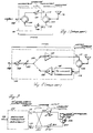
- FIGURE 1 schematically depicts a reciprocal hybrid mode element (RHYME) circuit of the type described in more detail at related US Patent Application Serial Number 07/330,638 referenced above. It employs standard microstrip circulators 100 and 102 together with a pair of hybrid mode non-reciprocal latchable phase shifters 104 and 106 (e.g., of the type described more fully in related US Patent Application Serial Number 07/330,617 cited above).
- RHYME reciprocal hybrid mode element
- a transmit/receive duplex port 108 in the microstrip mode provides input to a duplex radiator sub-module 110 comprising circulator 100 and latchable phase shifters 104, 106.
- This provides separate transmit and receive microstrip RF lines 112, 114 which, in conjunction with a conventional microstrip output circulator 102, communicate RF signals to/from a conventional RF radiator 116 (e.g., a waveguide radiator with a loop coupler connected to the microstrip output of circulator 102).
- a conventional RF radiator 116 e.g., a waveguide radiator with a loop coupler connected to the microstrip output of circulator 102).
- appropriate phase shifts are conventionally determined by an array controller computer (not shown) and then used to latch phase shifters 104, 106 at desired relative phase shifts for transmitting and receiving purposes in connection with each particular radiator 116.
- radiator transceive circuits 110 Similar phasing (and possibly amplitude control as well) is determined and latched into radiator transceive circuits 110 for all of the N1 x N2 radiators 116 of the array so as to define the appropriate radiation pattern shape, pointing angle, etc. This circuit will allow the same or different phases on transmit and receive without switching between transmit and receive.
- FIGURE 2 depicts a typical hybrid microwave integrated circuit (MIC) or monolithic microwave integrated circuit (MMIC) which provides implementation for the radiator transceive circuit 110.
- MIC or MMIC circuits are typically implemented on gallium arsenide substrates. They typically include a controllable integrated phase shifter 120, a controllable integrated attenuator 122, a controllable integrated transmit/receive switch 124, a relatively high power integrated amplifier 126 on the transmit leg of the MMIC with an integrated transmit/receive limiter 128 and integrated low noise amplifier 130 in the receive leg of the MMIC.
- the MMIC is typically mounted on a printed circuit board with microstrip mode input and output connections. Otherwise, the overall operation of the MMIC in FIGURE 2 (together with the usual circulator 102 and radiator 116) is similar to that of the RHYME circuit depicted and already described with respect to FIGURE 1.
- phased array there are numerous potential advantages to be had if one could quickly, efficiently and economically switch an entire phased array from operation in one polarization mode to operation in another different polarization mode.
- a phased array it is desirable, if possible, for a phased array to be capable of switching quickly and efficiently to any one of several different polarizations (e.g., linear vertical, linear horizontal, right-hand circular, left-hand circular).
- switchable control between different polarization modes for the array would be accomplished at the level of the individual radiating elements so that major feed and phase latching elements necessarily used to control the overall phased array may continue to conventionally operate using only one polarization or mode.
- a 90° microstrip coupling circuit for example a Lange coupler
- a pair of non-reciprocal latchable phase shifters e.g., capable of being latched to alternative relative phase shifts of 0° or 90°
- This circuit also accomplishes the duplexing (i.e., replaces the duplexing circulator).
- the RF radiator structure included with the module includes two orthogonal conductive coupling loops at one end of a circular waveguide. These loops are respectively coupled to microstrip outputs of latchable 0°, 90° phase shifters followed by a reciprocal dielectric quarter-wave plate and a non-reciprocal fixed ferrite quarter-wave plate (leading to the exit end of the circular waveguide).
- the coupling loops may be disposed in an air or other gas-filled (or vacuum) section of the circular waveguide, they are preferably potted with a solid dielectric material so that the entire RF radiator structure becomes a substantially solid monolithic cylinder that can thereafter be coated with an electrical conductor to define the conductive circular waveguide.
- a 90° Lange hybrid microstrip circuit as well as a pair of hybrid mode 0°, 90° phase shifters are disposed on a common printed circuit board which is physically attached to the non-radiating end of the waveguide radiator.
- Suitable latch wire driving circuitry for the 0°, 90° phase shifters may conveniently be disposed on the opposite side of the same printed circuit board to form a composite compact structure having an overall maximum diameter on the order of 0.6 wavelengths or less so that it may conveniently fit within the usual inter-radiator element spacing of a typical phased array.
- the cascaded 90° Lange hybrid microstrip circuit and a pair of 0°, 90° latchable phase shifters may be effectively substituted for the usual microstrip circulator used to couple the sub-module transmit and receive RF lines to the radiator structure within each RF radiator module.
- latch wire arrangements which could be used to latch the dual torids.
- a more conventional approach would be to drive each individual phase shifter separately and each phase shifter can be switched to its 0° or 90° state independently of the other.
- a particularly compact latch wire arrangement for the two 0°, 90° latchable phase shifters permits one of three predefined dual phase shifter states.
- the 0° state is defined as that state in which the phase shifter is latched to its electrically long state and therefore the 90° state is defined as that state in which the phase shifter is latched to its electrically short state.
- the length of the phase shifters is set so that the two states are 90° apart.
- the three predefined states of the phase shifters in the switch are 0°, 0°; 0°, 90°; and 90° 0°, to be easily actuated via a single latch wire. These states are usually actuated via one of the three latch wires.
- a pair of latching phase shifters may be latched in a 0°,0° state by one latch wire, and a 0°, 90° state by another latch wire and in a 90°, 0° state by yet a third latch wire.
- the same polarization as transmitted will be received in the receive path and the orthogonal polarization will be received in the transmit path.
- this may have special advantages for the RHYME or MMIC TR module. For example, if the input circulator of the RHYME is a four port circulator, the orthogonal polarization would be available at the fourth port. The transmit phase shifter would have to switch between transmit and receive to receive the orthogonal polarization looking in the same scan direction.
- the waveguide portion of the pair of hybrid mode phase shifters may be stacked on opposite sides of a common ground plane and used to directly feed a waveguide radiator (i.e., thereby obviating the microstrip mode at this end of the phase shifters) comprising, in seriatim, a dielectric septum polarizer, a reciprocal dielectric quarter-wave plate and a non-reciprocal ferrite quarter-wave plate.
- a waveguide radiator is preferably of square cross-section.
- a conventional radiator transceive sub-circuit 110 (e.g., like those depicted in FIGURES 1 and 2) is employed.
- a 90° Lange hybrid microstrip coupling circuit 300 is employed in cascade with a pair of non-reciprocal latchable hybrid mode phase shifters 302 and 304 to couple the radiator transceive sub-circuit 110 to a dual mode orthogonal radiator 306.
- the usual output circulator 102 has been effectively replaced with a 90° hybrid microstrip circuit and two 90° non-reciprocal latching hybrid mode phase shifters.
- An additional coupling loop for the other polarization of radiation is also added to a typical circular waveguide radiating element 306.
- the 90° Lange hybrid microstrip coupling circuit may be of the usual conventional type depicted at FIGURE 3A.
- FIGURE 3A For example, if a input RF signal of 0° phase is assumed to be input at port A, then reduced amplitude (-3dB) RF signals will be output at ports B and C with relative phase shifts of 0° and -90° respectively. Substantially zero RF power will be output from port D (i.e., it is "isolated") .
- the same sort of relative signal distribution will occur from the various input/output ports of such a coupling circuit when similar input signals are inserted at other of the ports.
- the non-reciprocal latchable hybrid mode phase shifters 302, 304 are, in this exemplary embodiment, preferably of the type disclosed more fully in related application Serial Number 07/330,617. However, they may be of relatively simple design so as to be capable of latching to produce relative phase shifts of only 0° or 90° in this exemplary embodiment.
- Such hybrid mode phase shifters include microstrip mode input and output circuits with a waveguide mode disposed in between.
- the waveguide mode includes a double toroid ferrite structure with suitable latch wires threaded therethrough so as to set the ferrite cores to desired states of remnant magnetization -- and thus to produce desired 0° or 90° relative phase shifts as RF signals traverse through the phase shifter structure.
- the non-reciprocal phase shifter can only be switched between 0° and 90° states, then it will automatically be set in the alternate phase state for signals passing in the reverse direction. That is, if a 0° phase shift is inserted in the forward or transmit direction, then without any need to reset its remnant flux, the phase shifter will produce a 90° phase shift for signals propagating in the reverse or receive direction. As will be appreciated later, for many of the exemplary embodiments this permits transceive operations for a selected polarization state without the need to switch the phase shifter(s) between transmit and receive operations.
- the microstrip outputs from phase shifters 302, 304 are connected to orthogonal current loops 308, 310 respectively in a dual mode orthogonal radiator 306 which may be a circular waveguide (i.e., the current loops 308, 310 excite appropriate orthogonal modes within the circular waveguide).
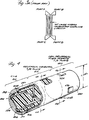
- a dual mode orthogonal circular waveguide radiator 306 is shown in more detail at FIGURE 4.
- a first section 400 contains conventional coupling loops 308, 310.
- each coupling loop conductor has a leg extending through a respective insulated aperture 402, 404 then proceeding in an inverted U-shaped locus to terminate at the opposite leg end by a connection to RF ground at 406, 408 respectively, (i.e., at the non-radiating end of waveguide 306).
- Each coupling loop 308, 310 has a total length of approximately one-half wavelength in the ambient medium surrounding such loops.
- the loops could be contained in vacuum, air, or other gases, in the exemplary embodiment they are preferably potted in a suitable solid dielectric (e.g., with a relative dielectric constant of approximately 6) which is finished to a cylindrical outer shape.
- exemplary waveguide 306 next includes a conventional reciprocal dielectric quarter-wave plate 420.
- the reciprocal dielectric quarter-wave plate includes a center slab 412 of relatively high dielectric constant (e.g., relative dielectric constant of about 16) while the dielectric 414 and 416 to either side of the central slab 412 are mode from a relatively lower dielectric constant material (e.g., relative dielectric constant of about 9).
- the higher dielectric constant slab 412 may be made, for example, from a magnesium titanate material while the outer sections 414, 416 may be made from an alumina material.
- the different materials may be epoxied together and glued (e.g., epoxied) in place adjacent section 400 of waveguide 306.
- the outer section 420 of waveguide 306 is a conventional non-reciprocal fixed ferrite quarter-wave plate.
- a cylindrical ferrite (e.g., a lithium ferrite for the X-band frequencies) 422 is surrounded by four magnets 424, 426, 428 and 430 poled as shown so as to produce magnetic fields 432 within the ferrite core 422 (as is conventionally known so as to produce the desired non-reciprocal fixed ferrite quarter wave plate structure).
- the quarter-wave plates 410 and 420 may be approximately 0.25 or 0.3 inches in length which approximates about one wavelength at X-band frequencies in these media.
- the sections 400, 410 and 420 of the waveguide 306 are suitably glued together (e.g., with epoxy) and, if not already of cylindrical form, ground into a round configuration, then they are suitably plated with a conductor (e.g., copper plated with gold flashing) to form an outer circular waveguide conductive wall 440 along the entire cylindrical outer structure of waveguide 306.
- a conductor e.g., copper plated with gold flashing
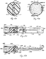
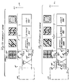
- FIGURES 5A-5D A schematic depiction of the physical appearance of the FIGURE 3 embodiment (using a RHYME radiator transceive sub-circuit 110) is depicted at FIGURES 5A-5D.
- the usual module microstrip input/output port 108 is connected to one port of a microstrip circulator 100.
- the other two circulator ports are respectively connected to the microstrip inputs of hybrid mode phase shifters 104, 106.
- the microstrip ports at the other end of phase shifters 104, 106 are connected to respective input/output ports of the 90° Lange hybrid microstrip coupling circuit 300.
- the 90° hybrid microstrip circuit 300 is then connected in cascade with the pair of 0°,90° hybrid mode phase shifters 302, 304 which, in turn, feed coupling loops 308, 310 via their microstrip terminations.
- the elements just described are mounted on a common printed circuit board 500 which is supported by flange 502 of the conductive non-radiating end piece termination 504 of waveguide 306.
- the usual circulator magnet 506 can also be seen in FIGURE 5B.
- the components 508 disposed on the underside of printed circuit board 500 may comprise the usual driving circuitry used to control the latch wires for hybrid mode phase shifters 104, 106 and 302, 304.
- driving circuitry may include the usual data latches, power drivers, etc., required for accepting commanded phase changes from a central phase array controller computer bus.
- Such commands are then executed by applying pulses of suitable current through latch wires in ferrite toroids so as to produce the desired remnant magnetization flux and to thus achieve the desired phase shift.
- Controllable attenuators could of course also be controlled in similar fashion by the driving circuitry 508.
- the overall diameter of the entire RF radiator module is sufficiently small that the modules can be easily packed at the desired inter element spacing within the phased array (e.g., typically less than 0.6 wavelength from center to center).
- the magnets 424, 426, 428 and 430 of the non-reciprocal fixed ferrite quarter wave plate 420 may be held in place by a suitable band 510.
- FIGURES 6A-6D uses the MMIC of FIGURE 2 as the radiator transceive sub-circuit 110.
- the transmit mode is depicted at FIGURE 6A.
- Hybrid mode phase shifters 302, 304 have been latched to the 0° and 90° phase shift states respectively. If it is assumed that a unit magnitude RF signal of 0° relative phase is present at transmit line 112 (as represented by the large vertical arrow with 0° nomenclature near its head), then the 90° hybrid microstrip coupling circuit 300 will provide reduced amplitude (-3dB) outputs on the right-side of the circuit 300 (represented by small arrows) which is connected in cascade with the pair of phase shifters 302-304.
- the relative phase of the input to phase shifter 302 is still 0° while the phase of signals input to phase shifter 304 is -90°.
- the RF signals actually presented to current loops 308, 310 are 0° and 0° respectively. That is, the RF signals fed to the two orthogonal current loops are in phase.
- the spatially orthogonal current loops 308, 310 are represented by spatially orthogonal vectors 308', 310' depicted to the right of radiator 306 in FIGURE 6A.
- the resultant vector sum 311' represents the actual linear vertical (LV) RF radiation transmitted from radiator 306.
- the reciprocal dielectric quarter wave plate 410 and the non-reciprocal fixed ferrite quarter-wave plate 420 may be omitted from the radiator 306 waveguide without charging the polarization of transmitted/received radiation.
- FIGURE 6B represents the same circuit configured for the receive mode.
- incoming linear vertically (LV) polarized radiation 313' is intercepted by the waveguide radiator 306 and resolved by orthogonal current loops 308, 310 to two components each having relative phases of 0° as indicated by the arrows and 0° depiction at the inputs of phase shifters 302, 304.
- the conventional reference point for observing the E-field vector polarization is to look toward the direction of propagation. Thus, for transmit modes, observation is away from the antenna and for receive modes observation is toward the antenna. To properly account for this convention, the left and right loop leg connections 308,310 are reversed for the receive modes when depicted in the FIGURES.
- phase shifters 302,304 are already in opposite phase states 90°,0° respectively. Thus, there is no need to switch flux remnant states in these phase shifters to permit reception in the same LV polarization mode.
- the input to the lower right-hand corner of the 90° hybrid microstrip coupling circuit 300 is still at 0° while the input at the upper right-hand corner of circuit 300 is now shifted -90°.
- the outputs at the upper left port will add destructively to zero while those at the lower left port will have a common relative phase of 0° and add constructively so as to provide a 0dB input at 0° relative phase to the receive RF channel 114 of the radiator transceive sub-circuit 110.
- FIGURES 6C and 6D show the same circuit configured respectively for transmit and receive modes but with phase shifters 302, 304 now set to produce linear horizontal (LH) modes of polarization.
- the transmit mode uses the 90°,0° phase states for phase shifters 302, 304.
- the RF signals now supplied to coupling loops 308, 310 have relative phase angles of +90° and -90°. Accordingly, vector summation of the signals actually radiated will produce linear horizontal (LH) RF output 311'.
- FIGURE 6B is automatically preset to the receive mode since phase shifters 302, 304 are already in the 0° and 90° phase shift states respectively for reverse or receive direction propagating signals.
- received LH polarized radiation 313' is resolved into orthogonal components by coupling loops 308, 310.
- vector analysis as indicated in FIGURE 6D shows signal progressions through phase shifters 302, 304 and the 90° Lange hybrid microstrip circuit 300. Duplexing operation is obtained by effective cancellation of signals at the upper left-hand port of circuit 300 and by constructive addition at the receive channel lower left-hand port of circuit 300 (now with a common +90° phase shift).
- FIGURES 6A-6D can also be used to provide right circular (RC) and left circular (LC) polarizations if the 0°, 90° phase shifters 302, 304 are replaced with 0°, ⁇ 90° phase shifters.
- RC right circular
- LC left circular
- the top phase shifter would be set to -90° and the bottom phase shifter would be set to 90°.
- These phase shifters would have to be switched for receiving RC polarization.
- For transmitting LC polarization both phase shifters would be set to 0°.
- the top phase shifter would be set to -90° and the bottom to +90°.
- phase shifters 302, 304 would preferably each be capable of effecting 0°, ⁇ 90° phase shifts. Using 0°, ⁇ 90°, all 4 polarizations can be obtained by discrete bit switching, no flux drive is required. This can best be illustrated by considering the following Table I.
- phasers 302,304 are provided in terms of relative phase shift and torid magnetization states (on opposite sides of the center dielectric septum of the polarizers) for various polarizations with comments as to whether switching is required between transmit and receive:
- FIGURES 7A-7F depict use of the RHYME radiator transceive sub-circuit 110.
- the very same sort of analysis for LV and LH polarization transmit and receive mode operations can be discerned from FIGURES 7A-7D.
- the reciprocal quarter wave plate 410 and non-reciprocal quarter wave plate 420 of radiator 306 are also depicted at the right-hand side of the FIGURE together with the vector representations 411 and 421 of signals at the exit face from each quarter-wave plate.
- these quarter-wave plates have no real effect as will be appreciated by those in the art.
- phase shifters 302,304 are in the 0° and 0° phase shift settings respectively for right circularly polarized radiation.
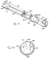
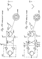
- FIGURE 8 depicts the rectangular waveguide portion of phase shifters 302, 304.
- Each waveguide includes the usual center dielectric slab 800 and pair of ferrite toroids 802,804.
- An exemplary pattern for winding latch wires 810, 820 and 830 through the toroid cores is also depicted in FIGURE 8.
- a suitable power source 840 in conjunction with suitable conventional driving circuits and electronic switches (schematically depicted by simplified unipolar switches 842, 843 and 844) may be used in conjunction with a single sense wire to set the pair of phase shifters 302, 304 to appropriate pairs of phase shifting states.
- latch wire 810 may be used to simultaneously set both phase shifters 302, 304 to produce forward-direction (i.e., transmit) phase shifts of 0° and 90° respectively.
- latch wire 820 may be used to set the pair of phase shifters 302, 304 to the forward direction phase states 0°,0° and latch wire 830 may be used to set the pair of phase shifters 302,304 to the forward direction phase states 90°,0° respectively.
- the actual drive circuits would be capable of bi-polar operation so as to establish a current pulse of the correct magnitude, duration and polarity to set a proper magnitude and polarity of remnant flux in the ferrite toroids.
- the usual RHYME radiator transceive sub-circuit 110 has been modified so that circulator 100' has a fourth port 150 disposed between the usual transmit/receive RF channel ports.
- port 150 provides for reception of any incoming radiation having orthogonal circular polarization to that for which the RF radiator module is currently set.
- FIGURES 10 and 11A-11F represents an alternative embodiment wherein the waveguides of the hybrid mode phase shifters 302,304 are stacked one on top of the other (on opposite sides of a common ground plane) and used to directly feed a square waveguide radiator 306'.
- a conventional septum polarizer is utilized to provide dual mode orthogonal radiation modes rather than a pair of orthogonal coupling loops.
- the operation of the dielectric quarter-wave plate 410' and of the non-reciprocal ferrite quarter-wave plate 420' is as previously discussed.
- Cross-sectional depictions are depicted at FIGURES 10A-10C as should now be apparent.
- the arrayed waveguides of phase shifters 302,304 are also depicted in cross-section on opposite sides of a common ground plane 1100 in FIGURES 11A-11F.
- microstrip to square waveguide transition is accomplished with the hybrid mode phase shifters 302,304 directly.
- a transmit and receive microstrip line present at the other ends of phase shifters 302, 304.
- This polarization switching technique differs from others in part because it requires a septum polarizer.
- the microstrip feedlines to the other end of the hybrid mode phase shifters 302, 304 must have one of these lines routed through the ground plane substrate so as to interface with the hybrid mode 90° phase shifter located on the opposite side from the remainder of the microstrip circuitry (e.g., the 90° Lange microstrip hybrid, the other conventional phase shifting circuits, etc.).
- the hybrid mode 90° phase shifter located on the opposite side from the remainder of the microstrip circuitry (e.g., the 90° Lange microstrip hybrid, the other conventional phase shifting circuits, etc.).
- a transmit mode for linear vertical polarized radiation can be obtained by setting phase shifters 302,304 to the 0° and 90° phase states respectively.
- a receive mode for the same polarization can be automatically achieved since the phase shifters 302,304 are already in reverse or receive direction 90°,0° phase states respectively.
- Transmit and receive modes for linear horizontal polarizations are just the reverse as depicted in FIGURES 11C and 11D.
- phase shifters 302, 304 are set to the 0° and 0° phase states respectively as depicted in FIGURE 11E.
- phase shifters 302, 304 are thus already at the proper reverse or receive direction 90° and 90° phase states respectively as depicted at FIGURE 11F.
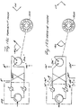
- FIGURE 12 Yet another embodiment is depicted at FIGURE 12.
- the 0°,90° phase shifters 302, 304 are omitted and an electrically rotatable ferrite quarter-wave plate radiating element 1200 is employed in the circular waveguide radiator 306''.
- the quadupole field of radiator element 1200 may be electrically rotated to produce any linear polarization from linear vertical to linear horizontal. This permits transmission of any desired linear polarization and reception of the same polarization while also achieving desired duplexing operation.
- the rotary field device itself as a half-wave plate device has previously been described by Fox, A.G., "Adjustable Waveguide Phase Changer," Proceedings IRE , Vol.
- FIGURE 13 The presently utilized quarter-wavelength version of this device is depicted at FIGURE 13. Like its half-wave cousin, it utilizes two windings 1300, 1302 located on a stator yoke 1304 surrounding a completely filled ferrite circular waveguide 1306 as depicted in cross-section and in schematic form at FIGURE 13. Windings 1300, 1302 are associated with alternate poles of yoke 1304 and excited with respective sine and cosine current functions as indicated in FIGURE 13.
- FIGURES 12A-12D use the same nomenclature already explained to analyze the operation of the FIGURE 12 circuit for both transmit and receive modes in linear vertical and linear horizontal radiation modes. It should be appreciated that any rotation of this linear polarization can be achieved by suitably exciting the windings in the electrically rotatable ferrite quarter wave plate radiator 1200.
- polarization agile operation over a very broad bandwidth (e.g., 3 to 1) should be possible. Such an approach may produce approximately the same overall insertion losses as the use of the duplexing output circulator 102 being replaced by these polarization agile circuits.
- the "up-up" switching technique of the driver described in related US Patent Application 07/333,961 may be utilized.
- the non-reciprocal ferrite quarter wave plate could have other conventional (e.g., electrically "long") states of magnetization so as to achieve the desired difference in propagation constants for LV and LH polarized inputs components (thereby causing the output to be polarized as a function of phase difference as will be recognized by those in the art).
- the operation of the polarization switch or phase gradient for the phased array can still be attained as should be appreciated by those in the art.
- the latchable phase shifters 302, 304 may be capable of switching in less than one microsecond and require less than 20 microjoules to switch at either X-band or Ku-band frequencies. This is believed to be an advantage over prior techniques (e.g., using Faraday rotators, switchable quarter-wave plates, etc.).
- the polarization switching schemes described above are microstrip compatible and therefore can be used in conjunction with either conventional RHYME or MMIC radiator transceive sub-circuits.
- the cross-sectional dimensions of the entire polarization agile RF radiator modules are well within the range of inter-element spacings typically required in phased arrays at either X-band or Ku-band frequencies (e.g., less than about 0.6 wavelength).
- Additional RF loses required to achieve polarization agility in accordance with at least some embodiments of this invention are presently estimated to be on the order of only about 0.2dB (e.g., assuming that the conventional RHYME or MMIC radiator transceive sub-circuits 110 are employed as discussed above).
- the 0.2dB value has been estimated by calculating and comparing losses using a duplexing output circulator 102 as done conventionally on the one hand and a polarization switch using latchable phase shifters 302, 304, etc., as previously described. For example, consider the following calculation:
- the quarter-wave plates may be eliminated and the estimated additional insertion loss suffered to achieve such polarization diversity may be only on the order of 0.05dB.
- a polarization switch may include a microstrip input feeding a dual-polarized notch radiating element. Such device will selectively transmit and receive LV or LH polarization and also accomplish duplexing at the following presently estimated specifications: PARAMETER VALUE Frequency Range 7 - 11 GHz Insertion Loss ⁇ 0.5 dB VSWR ⁇ 1.2:1 Switching Time ⁇ 0.5 ⁇ sec Switching Energy ⁇ 15 ⁇ joules Peak Power 200W Average Power 20W Size 0.5 x 0.2 x 0.5 Weight ⁇ 2 gm
Abstract
Description
- This invention relates generally to RF radiator modules for use in a phased array. More particularly, this invention provides polarization agility for such modules in advantageous spatially compact, economical and relatively easily implemented embodiments.
- This application is related to the following commonly assigned US patents and patent applications:
U.S. Patent No. 4,445,098 - Sharon et al (1984)
U.S. Patent No. 4,884,045 - Alverson et al (1989)
USSN 07/330,638 filed March 30, 1989 naming Roger G. Roberts as inventor and entitled "Reciprocal Hybrid Mode RF Circuit for Coupling RF Transmission to an RF Radiator;"
USSN 07/330,617 filed March 30, 1989 naming Roger G. Roberts et al as inventors and entitled "Hybrid Mode RF Phase Shifter and Variable Power Divider Using the Same" (to be issued December 24, 1991 as U.S. Patent No. 5,075,648);
USSN 07/333,961 filed April 6, 1989 naming David W. Wallis et al as inventors and entitled "Simplified Driver For Controlled Flux Ferrite 525 Phase Shifter" (allowed June 4, 1991);
USSN 07/669,959 filed March 15, 1991 as a CIP of Serial No. 07/330,617, naming Roger G. Roberts et al as inventors and entitled "Single Toroid Hybrid Mode RF Phase Shifter." - The entire contents of all the above-listed patents and patent applications are hereby incorporated by reference
- Phased arrays of RF radiators are by now well-known in the art. In general, such arrays may comprise a two-dimensional array of N₁ x N₂ RF radiators, each capable of transmitting/receiving RF electromagnetic signals propagated through space. By judiciously spacing and locating each individual radiator in the array and by carefully controlling the relative phasing of RF electrical signals being fed to and from each of the radiators over the entire array aperture, an array "phase gradient" can be defined. By also carefully controlling the relative amplitude or attenuation of RF electrical signals being fed to and from each radiator over the entire array aperture an "amplitude taper" also may be defined. One may quite precisely define the overall radiation pattern configuration and orientation by properly controlling the relative phase and amplitude of each radiator module. The amplitude taper is usually designed into the feeding network and a variable phase gradient is obtained by RF phase shifters. For example, by appropriately controlling (i.e., changing) the phase settings of radiators in such an array, a well-defined beam radiation pattern may be electronically pointed over a major portion of a hemisphere without any mechanical movement of the array or any of the arrayed radiator elements.
- Such phased arrays may be utilized, for example, in airborne, ground-based, space platform based, etc. locations. One application may be a radar system where a radar RF transmitter/receiver system uses the entire phased array as a common RF transmit/receive transducer with a relatively narrow "pencil beam" radiation pattern that can be shaped and pointed electronically as desired by appropriate and timely computer control of the relative phases (and, if desired, amplitudes) of RF signals being transmitted/received at each individual radiator site.
- Conventional duplex RF radiator modules for use in a phased array may be of many different types. However, two currently typical types are depicted in FIGURES 1 and 2. FIGURE 1 schematically depicts a reciprocal hybrid mode element (RHYME) circuit of the type described in more detail at related US Patent Application Serial Number 07/330,638 referenced above. It employs
standard microstrip circulators latchable phase shifters 104 and 106 (e.g., of the type described more fully in related US Patent Application Serial Number 07/330,617 cited above). Thus, a transmit/receiveduplex port 108 in the microstrip mode provides input to aduplex radiator sub-module 110 comprisingcirculator 100 andlatchable phase shifters microstrip RF lines microstrip output circulator 102, communicate RF signals to/from a conventional RF radiator 116 (e.g., a waveguide radiator with a loop coupler connected to the microstrip output of circulator 102). As will be appreciated by those in the art, appropriate phase shifts are conventionally determined by an array controller computer (not shown) and then used tolatch phase shifters particular radiator 116. Similar phasing (and possibly amplitude control as well) is determined and latched into radiatortransceive circuits 110 for all of the N₁ xN₂ radiators 116 of the array so as to define the appropriate radiation pattern shape, pointing angle, etc. This circuit will allow the same or different phases on transmit and receive without switching between transmit and receive. - FIGURE 2 depicts a typical hybrid microwave integrated circuit (MIC) or monolithic microwave integrated circuit (MMIC) which provides implementation for the
radiator transceive circuit 110. Such MIC or MMIC circuits are typically implemented on gallium arsenide substrates. They typically include a controllable integratedphase shifter 120, a controllable integratedattenuator 122, a controllable integrated transmit/receive switch 124, a relatively high power integratedamplifier 126 on the transmit leg of the MMIC with an integrated transmit/receivelimiter 128 and integratedlow noise amplifier 130 in the receive leg of the MMIC. The MMIC is typically mounted on a printed circuit board with microstrip mode input and output connections. Otherwise, the overall operation of the MMIC in FIGURE 2 (together with theusual circulator 102 and radiator 116) is similar to that of the RHYME circuit depicted and already described with respect to FIGURE 1. - Increasingly, it is desirable to permit controlled change in the spatial polarization of electromagnetic RF signals transmitted/received to/from
radiators 116 of a phased array. For example, good radar performance during bad weather conditions may require the radar to transmit in a first sense circular polarization (e.g., left-hand circular polarization) and to receive the same sense circular polarization (e.g., left-hand circular polarization). Rain clutter signals will return with an opposite sense circular polarization (e.g., right-hand circular polarization) and therefore be rejected. On the other hand, radar return from man-made clutter may tend to be stronger for linear vertical or linear horizontal polarizations of electromagnetic signals. As those in the art will appreciate, there are numerous potential advantages to be had if one could quickly, efficiently and economically switch an entire phased array from operation in one polarization mode to operation in another different polarization mode. In particular, it is desirable, if possible, for a phased array to be capable of switching quickly and efficiently to any one of several different polarizations (e.g., linear vertical, linear horizontal, right-hand circular, left-hand circular). Most desirably, such switchable control between different polarization modes for the array would be accomplished at the level of the individual radiating elements so that major feed and phase latching elements necessarily used to control the overall phased array may continue to conventionally operate using only one polarization or mode. - Typical prior art approaches for achieving polarization switching at a radiator element level involve the use of switchable ferrite quarter wave plates or 45° Faraday rotators in conjunction with a reciprocal quarter wave plate. These devices are typically quite slow in switching speed (e.g., typical switching times are on the order of 100 microseconds or so). Further details of such prior art approaches can be had by reference to U.S. Patent No. 3,698,008 - Roberts et al, issued October 10, 1972 entitled "Latchable, Polarization-Agile Reciprocal Phase Shifter."
-
- We have now discovered that a 90° microstrip coupling circuit (for example a Lange coupler) cascaded with a pair of non-reciprocal latchable phase shifters (e.g., capable of being latched to alternative relative phase shifts of 0° or 90°) may be used in conjunction with a dual orthogonal radiator to achieve more economic and rapid polarization agility (e.g., in conjunction with a RHYME circuit or an MMIC or other similar radiator transceive circuits). This circuit also accomplishes the duplexing (i.e., replaces the duplexing circulator).
- In one exemplary embodiment, the RF radiator structure included with the module includes two orthogonal conductive coupling loops at one end of a circular waveguide. These loops are respectively coupled to microstrip outputs of latchable 0°, 90° phase shifters followed by a reciprocal dielectric quarter-wave plate and a non-reciprocal fixed ferrite quarter-wave plate (leading to the exit end of the circular waveguide). Although the coupling loops may be disposed in an air or other gas-filled (or vacuum) section of the circular waveguide, they are preferably potted with a solid dielectric material so that the entire RF radiator structure becomes a substantially solid monolithic cylinder that can thereafter be coated with an electrical conductor to define the conductive circular waveguide. Of course the usual permanent magnets would also be arrayed circumferentially about the non-reciprocal fixed ferrite quarter-wave plate portion of waveguide as will be appreciated by those in the art. This circuit will accept a microstrip input and switch to linear vertical, linear horizontal or one sense circular at the output. The same polarization will be received as transmitted with duplexing, no switching being required between transmit and receive.
- Preferably, a 90° Lange hybrid microstrip circuit as well as a pair of
hybrid mode 0°, 90° phase shifters are disposed on a common printed circuit board which is physically attached to the non-radiating end of the waveguide radiator. Suitable latch wire driving circuitry for the 0°, 90° phase shifters (as well as the usual more versatile controllable phase shifters associated with each radiating module) may conveniently be disposed on the opposite side of the same printed circuit board to form a composite compact structure having an overall maximum diameter on the order of 0.6 wavelengths or less so that it may conveniently fit within the usual inter-radiator element spacing of a typical phased array. - For use with the usual RHYME or MMIC radiator transceive sub-module circuits, the cascaded 90° Lange hybrid microstrip circuit and a pair of 0°, 90° latchable phase shifters may be effectively substituted for the usual microstrip circulator used to couple the sub-module transmit and receive RF lines to the radiator structure within each RF radiator module.
- There are a number of latch wire arrangements which could be used to latch the dual torids. A more conventional approach would be to drive each individual phase shifter separately and each phase shifter can be switched to its 0° or 90° state independently of the other.
- A particularly compact latch wire arrangement for the two 0°, 90° latchable phase shifters permits one of three predefined dual phase shifter states. The 0° state is defined as that state in which the phase shifter is latched to its electrically long state and therefore the 90° state is defined as that state in which the phase shifter is latched to its electrically short state. The length of the phase shifters is set so that the two states are 90° apart. The three predefined states of the phase shifters in the switch are 0°, 0°; 0°, 90°; and 90° 0°, to be easily actuated via a single latch wire. These states are usually actuated via one of the three latch wires. For example, a pair of latching phase shifters may be latched in a 0°,0° state by one latch wire, and a 0°, 90° state by another latch wire and in a 90°, 0° state by yet a third latch wire.
- When this polarization switching technique is used, the same polarization as transmitted will be received in the receive path and the orthogonal polarization will be received in the transmit path. As will be appreciated, this may have special advantages for the RHYME or MMIC TR module. For example, if the input circulator of the RHYME is a four port circulator, the orthogonal polarization would be available at the fourth port. The transmit phase shifter would have to switch between transmit and receive to receive the orthogonal polarization looking in the same scan direction.
- If desired, the waveguide portion of the pair of hybrid mode phase shifters may be stacked on opposite sides of a common ground plane and used to directly feed a waveguide radiator (i.e., thereby obviating the microstrip mode at this end of the phase shifters) comprising, in seriatim, a dielectric septum polarizer, a reciprocal dielectric quarter-wave plate and a non-reciprocal ferrite quarter-wave plate. This avoids transitions to microstrip and back to waveguide modes, the use of coupling loops in the non-radiating end of the waveguide radiator, etc. In this embodiment, the waveguide radiator is preferably of square cross-section.
- The use of a 90° Lange hybrid microstrip circuit even without extra 0°, 90° phase shifters but, instead, in conjunction with an electrically rotatable ferrite quarter-wave plate radiating element may also achieve polarization agility with respect to at least linear polarizations of transmitted/received electromagnetic radiation.
- These as well as other objects and advantages of this invention will be more completely understood and appreciated by careful study of the following detailed description of several exemplary embodiments of this invention when taken in conjunction with the accompanying drawings, of which:
- FIGURE 1 is a schematic diagram of a typical prior art reciprocal hybrid mode element (RHYME) circuit for one radiator element of a phased array;
- FIGURE 2 is a schematic depiction of a typical prior art monolithic microwave integrated circuit (MMIC) radiator transceive circuit also to be utilized for a single radiator element of a phased array;
- FIGURE 3 is a schematic depiction of a 90° Lange hybrid microstrip coupling circuit cascaded with a pair of 0°,90° latchable phase shifters and a suitable radiator transceive sub-circuit interfaced with a dual mode orthogonal radiator in accordance with a first exemplary embodiment of this invention;
- FIGURE 3A is a schematic depiction of a typical 90° Lange hybrid microstrip coupling circuit;
- FIGURE 4 is a schematic perspective view of a dual mode orthogonal circular waveguide radiator which may be used with the FIGURE 3 embodiment of this invention;
- FIGURES 4A and 4B are cross-sectional depictions of the radiator depicted at FIGURE 4;
- FIGURES 5A, 5B, 5C and 5D are top, side, perspective and schematic end views respectively of a polarization agile duplex RF radiator module for use in a phased array in accordance with this invention utilizing the radiator of FIGURE 4, a RHYME radiator transceive sub-circuit (from FIGURE 1) in the exemplary embodiment depicted at FIGURE 3;
- FIGURES 6A, 6B, 6C and 6D are schematic depictions of the FIGURE 3 embodiment using an MMIC transceive sub-circuits in transmit and receive modes for both (i) linear vertical and (ii) linear horizontal polarization modes respectively;
- FIGURES 7A, 7B, 7C, 7D, 7E and 7F schematically depict the FIGURE 3 embodiment using a RHYME and illustrating both transmit and receive modes for (i) linear vertical, (ii) linear horizontal and right-hand circularly polarized polarization;
- FIGURE 8 is a schematic perspective view of exemplary latch wire driving and threading of the double toroid ferrite phase shifter structures utilized in the pair of 0°,90° latchable phase shifters employed in the exemplary embodiment of FIGURE 3;
- FIGURE 9 is a schematic depiction of yet a further modification to the embodiment of FIGURES 7A-7E wherein a four port circulator is used in the RHYME transceive sub-circuit to provide a received orthogonal polarization port;
- FIGURE 10 generally depicts yet another embodiment of this invention wherein a square waveguide radiator structure is directly coupled to the waveguide portions of a pair of 0°, 90° hybrid mode phase shifters;
- FIGURES 10A, 10B and 10C are cross sectional depictions at various points in the square waveguide structure of FIGURE 10;
- FIGURES 11A, 11B, 11C, 11D, 11E and 11F are schematic depictions of the FIGURE 10 embodiment set up for both transmit and receive modes in (i) linear vertical, (ii) linear horizontal and (iii) left-hand circularly polarized modes of operation;
- FIGURE 12 is a schematic depiction of yet another embodiment of this invention wherein a 90° Lange hybrid microstrip coupling circuit is used in conjunction with an electrically rotatable ferrite quarter wave plate radiating element to achieve linear polarization agility;
- FIGURES 12A, 12B, 12C and 12D schematically depict both transmit and receive modes (i) for linear vertical and (ii) linear horizontal operation of the FIGURE 12 embodiment; and
- FIGURE 13 is a schematic depiction of the electrically rotatable ferrite quarter wave plate radiating element so as to better explain the generation of rotatable fields in the quarter wave plate ferrite material.
- In the exemplary embodiment of FIGURE 3, a conventional radiator transceive sub-circuit 110 (e.g., like those depicted in FIGURES 1 and 2) is employed. However, instead of the usual
output microstrip circulator 102 coupling transmit/receiveRF lines microstrip coupling circuit 300 is employed in cascade with a pair of non-reciprocal latchable hybridmode phase shifters radiator transceive sub-circuit 110 to a dual modeorthogonal radiator 306. - In the exemplary embodiment of FIGURE 3, the
usual output circulator 102 has been effectively replaced with a 90° hybrid microstrip circuit and two 90° non-reciprocal latching hybrid mode phase shifters. An additional coupling loop for the other polarization of radiation is also added to a typical circularwaveguide radiating element 306. - The 90° Lange hybrid microstrip coupling circuit may be of the usual conventional type depicted at FIGURE 3A. Here, for example, if a input RF signal of 0° phase is assumed to be input at port A, then reduced amplitude (-3dB) RF signals will be output at ports B and C with relative phase shifts of 0° and -90° respectively. Substantially zero RF power will be output from port D (i.e., it is "isolated") . As is recognized by those in the art, the same sort of relative signal distribution will occur from the various input/output ports of such a coupling circuit when similar input signals are inserted at other of the ports. For example, if a
unit magnitude 0° relative phase RF signal is input at port D, then reduced amplitude (-3dB) signals will be output from ports C and B with relative phases of 0° and -90° respectively (there being essentially zero output from port A as a result of inputs to port D). Similar suitable 90° coupling circuits may also be known to those in the art. - The non-reciprocal latchable hybrid
mode phase shifters - In the exemplary embodiment of FIGURE 3, the microstrip outputs from
phase shifters current loops orthogonal radiator 306 which may be a circular waveguide (i.e., thecurrent loops circular waveguide radiator 306 is shown in more detail at FIGURE 4. Here, afirst section 400 containsconventional coupling loops insulated aperture coupling loop - Outwardly from
section 400,exemplary waveguide 306 next includes a conventional reciprocal dielectric quarter-wave plate 420. As shown in the cross-sectional depiction at FIGURE 4A, the reciprocal dielectric quarter-wave plate includes acenter slab 412 of relatively high dielectric constant (e.g., relative dielectric constant of about 16) while the dielectric 414 and 416 to either side of thecentral slab 412 are mode from a relatively lower dielectric constant material (e.g., relative dielectric constant of about 9). The higher dielectricconstant slab 412 may be made, for example, from a magnesium titanate material while theouter sections adjacent section 400 ofwaveguide 306. - Finally, the
outer section 420 ofwaveguide 306 is a conventional non-reciprocal fixed ferrite quarter-wave plate. As shown in the cross sectional depiction in FIGURE 4B, a cylindrical ferrite (e.g., a lithium ferrite for the X-band frequencies) 422 is surrounded by fourmagnets wave plates - After the
sections waveguide 306 are suitably glued together (e.g., with epoxy) and, if not already of cylindrical form, ground into a round configuration, then they are suitably plated with a conductor (e.g., copper plated with gold flashing) to form an outer circular waveguideconductive wall 440 along the entire cylindrical outer structure ofwaveguide 306. Since the design and functioning of such reciprocal dielectric quarter-wave plates and non-reciprocal fixed ferrite quarter-wave plates are well-known to those in the art, no further details are believed to be necessary. As will be appreciated, the RF radiation will actually emanate from the right-hand end ofcircular waveguide 306 as depicted at FIGURE 4.
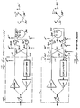
A schematic depiction of the physical appearance of the FIGURE 3 embodiment (using a RHYME radiator transceive sub-circuit 110) is depicted at FIGURES 5A-5D. As shown in FIGURE 5A, the usual module microstrip input/output port 108 is connected to one port of amicrostrip circulator 100. The other two circulator ports are respectively connected to the microstrip inputs of hybridmode phase shifters phase shifters microstrip coupling circuit 300. The 90°hybrid microstrip circuit 300 is then connected in cascade with the pair of 0°,90° hybridmode phase shifters feed coupling loops - As can be seen in the side view of FIGURE 5B, the elements just described (e.g., microstrip and/or hybrid mode phase shifters) are mounted on a common printed
circuit board 500 which is supported byflange 502 of the conductive non-radiatingend piece termination 504 ofwaveguide 306. Theusual circulator magnet 506 can also be seen in FIGURE 5B. Thecomponents 508 disposed on the underside of printedcircuit board 500 may comprise the usual driving circuitry used to control the latch wires for hybridmode phase shifters circuitry 508. As may be seen by the typical wavelength dimensions in FIGURES 5A-5D, the overall diameter of the entire RF radiator module is sufficiently small that the modules can be easily packed at the desired inter element spacing within the phased array (e.g., typically less than 0.6 wavelength from center to center). - As also depicted in FIGURES 5A-5D, the
magnets quarter wave plate 420 may be held in place by asuitable band 510. - The exemplary embodiment of FIGURES 6A-6D uses the MMIC of FIGURE 2 as the
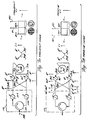
radiator transceive sub-circuit 110. Here, the transmit mode is depicted at FIGURE 6A. Hybridmode phase shifters microstrip coupling circuit 300 will provide reduced amplitude (-3dB) outputs on the right-side of the circuit 300 (represented by small arrows) which is connected in cascade with the pair of phase shifters 302-304. As indicated by nomenclature at the head of the reduced amplitude arrows at these ports in FIGURE 6A, the relative phase of the input to phaseshifter 302 is still 0° while the phase of signals input tophase shifter 304 is -90°. With thelatchable phase shifters current loops 308, 310 (schematically represented as a bottom view of the loop legs going into insulated apertures inbase 504 of waveguide 306) are 0° and 0° respectively. That is, the RF signals fed to the two orthogonal current loops are in phase. The spatially orthogonalcurrent loops radiator 306 in FIGURE 6A. As can be appreciated, the resultant vector sum 311' represents the actual linear vertical (LV) RF radiation transmitted fromradiator 306. As will also be appreciated by those in the art, in the case of linear vertical (LV) and linear horizontal (LH) radiation, the reciprocal dielectricquarter wave plate 410 and the non-reciprocal fixed ferrite quarter-wave plate 420 may be omitted from theradiator 306 waveguide without charging the polarization of transmitted/received radiation. - FIGURE 6B represents the same circuit configured for the receive mode. Here, incoming linear vertically (LV) polarized radiation 313' is intercepted by the
waveguide radiator 306 and resolved by orthogonalcurrent loops phase shifters - As already explained, for the reverse or receive direction of propagation, phase shifters 302,304 are already in opposite phase states 90°,0° respectively. Thus, there is no need to switch flux remnant states in these phase shifters to permit reception in the same LV polarization mode. The input to the lower right-hand corner of the 90° hybrid
microstrip coupling circuit 300 is still at 0° while the input at the upper right-hand corner ofcircuit 300 is now shifted -90°. As a result of these two inputs to the 90°hybrid microstrip coupler 300, the outputs at the upper left port will add destructively to zero while those at the lower left port will have a common relative phase of 0° and add constructively so as to provide a 0dB input at 0° relative phase to the receiveRF channel 114 of theradiator transceive sub-circuit 110. - FIGURES 6C and 6D show the same circuit configured respectively for transmit and receive modes but with
phase shifters phase shifters coupling loops - Similarly, FIGURE 6B is automatically preset to the receive mode since
phase shifters loops phase shifters hybrid microstrip circuit 300. Duplexing operation is obtained by effective cancellation of signals at the upper left-hand port ofcircuit 300 and by constructive addition at the receive channel lower left-hand port of circuit 300 (now with a common +90° phase shift). - The circuitry of FIGURES 6A-6D can also be used to provide right circular (RC) and left circular (LC) polarizations if the 0°, 90°
phase shifters phase shifters - In the following table, the states for phasers 302,304 are provided in terms of relative phase shift and torid magnetization states (on opposite sides of the center dielectric septum of the polarizers) for various polarizations with comments as to whether switching is required between transmit and receive:

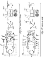
- FIGURES 7A-7F depict use of the RHYME
radiator transceive sub-circuit 110. Here, the very same sort of analysis for LV and LH polarization transmit and receive mode operations can be discerned from FIGURES 7A-7D. For completeness, the reciprocalquarter wave plate 410 and non-reciprocalquarter wave plate 420 ofradiator 306 are also depicted at the right-hand side of the FIGURE together with thevector representations - However, in FIGURES 7E and 7F, it can be seen that the
quarter wave plates coupling loops 308, 310). As will be observed, phase shifters 302,304 are in the 0° and 0° phase shift settings respectively for right circularly polarized radiation. - FIGURE 8 depicts the rectangular waveguide portion of
phase shifters dielectric slab 800 and pair of ferrite toroids 802,804. An exemplary pattern for windinglatch wires suitable power source 840 in conjunction with suitable conventional driving circuits and electronic switches (schematically depicted by simplifiedunipolar switches 842, 843 and 844) may be used in conjunction with a single sense wire to set the pair ofphase shifters latch wire 810 may be used to simultaneously set bothphase shifters latch wire 820 may be used to set the pair ofphase shifters latch wire 830 may be used to set the pair of phase shifters 302,304 to the forward direction phase states 90°,0° respectively. As will be appreciated the actual drive circuits would be capable of bi-polar operation so as to establish a current pulse of the correct magnitude, duration and polarity to set a proper magnitude and polarity of remnant flux in the ferrite toroids. - In FIGURE 9, the usual RHYME
radiator transceive sub-circuit 110 has been modified so that circulator 100' has a fourth port 150 disposed between the usual transmit/receive RF channel ports. When this arrangement is used in connection with circularly polarized radiation, port 150 provides for reception of any incoming radiation having orthogonal circular polarization to that for which the RF radiator module is currently set. - The embodiment of FIGURES 10 and 11A-11F represents an alternative embodiment wherein the waveguides of the hybrid mode phase shifters 302,304 are stacked one on top of the other (on opposite sides of a common ground plane) and used to directly feed a square waveguide radiator 306'. Here, a conventional septum polarizer is utilized to provide dual mode orthogonal radiation modes rather than a pair of orthogonal coupling loops. A more complete understanding of this reciprocal phase shifter arrangement of a pair of phase shifters in a square geometry coupled to a septum polarizer can be had from related US Patent No. 4,884,045 - Alverson et al referenced above. The operation of the dielectric quarter-wave plate 410' and of the non-reciprocal ferrite quarter-wave plate 420' is as previously discussed. Cross-sectional depictions are depicted at FIGURES 10A-10C as should now be apparent. The arrayed waveguides of phase shifters 302,304 are also depicted in cross-section on opposite sides of a
common ground plane 1100 in FIGURES 11A-11F. - Here, the microstrip to square waveguide transition is accomplished with the hybrid mode phase shifters 302,304 directly. There is, of course, a transmit and receive microstrip line present at the other ends of
phase shifters phase shifters mode phase shifters hybrid mode 90° phase shifter located on the opposite side from the remainder of the microstrip circuitry (e.g., the 90° Lange microstrip hybrid, the other conventional phase shifting circuits, etc.). - As may be seen by inspection of the FIGURES, the representative phase settings for phase shifters 302,304 and the usual vector notations introduced for other embodiments, a transmit mode for linear vertical polarized radiation can be obtained by setting phase shifters 302,304 to the 0° and 90° phase states respectively. Similarly, a receive mode for the same polarization can be automatically achieved since the phase shifters 302,304 are already in reverse or receive
direction 90°,0° phase states respectively. Transmit and receive modes for linear horizontal polarizations are just the reverse as depicted in FIGURES 11C and 11D. For transmitting left circular (LC) polarization,phase shifters phase shifters direction 90° and 90° phase states respectively as depicted at FIGURE 11F. - Yet another embodiment is depicted at FIGURE 12. Here the 0°,90°
phase shifters plate radiating element 1200 is employed in the circular waveguide radiator 306''. The quadupole field ofradiator element 1200 may be electrically rotated to produce any linear polarization from linear vertical to linear horizontal. This permits transmission of any desired linear polarization and reception of the same polarization while also achieving desired duplexing operation. The rotary field device itself as a half-wave plate device has previously been described by Fox, A.G., "Adjustable Waveguide Phase Changer," Proceedings IRE, Vol. 35, December 1947 and Fox et al, "Behavior and Application of Ferrites," The Bell System Technical Journal, Vol. XXXIV, No. 1, January 1955. The presently utilized quarter-wavelength version of this device is depicted at FIGURE 13. Like its half-wave cousin, it utilizes twowindings 1300, 1302 located on astator yoke 1304 surrounding a completely filledferrite circular waveguide 1306 as depicted in cross-section and in schematic form at FIGURE 13.Windings 1300, 1302 are associated with alternate poles ofyoke 1304 and excited with respective sine and cosine current functions as indicated in FIGURE 13. When winding currents are varied as the sine and cosine, the field will rotate and therefore the linearly polarized wave emanating from this quarter wave plate radiator will also rotate. Duplexing may be accomplished because such rotary field quarter wave plate is inherently non-reciprocal. At the same time, it is non-latching and also slow to switch. It will be appreciated by those in the art, that by properly phasing the sine and cosine currents applied to these two windings, proper rotation of the polarization may be obtained. - FIGURES 12A-12D use the same nomenclature already explained to analyze the operation of the FIGURE 12 circuit for both transmit and receive modes in linear vertical and linear horizontal radiation modes. It should be appreciated that any rotation of this linear polarization can be achieved by suitably exciting the windings in the electrically rotatable ferrite quarter
wave plate radiator 1200. - If the MMIC
radiator transceive sub-circuit 110 is utilized in conjunction with a notched radiator, then polarization agile operation over a very broad bandwidth (e.g., 3 to 1) should be possible. Such an approach may produce approximately the same overall insertion losses as the use of theduplexing output circulator 102 being replaced by these polarization agile circuits. - To attain the fastest possible switching of the
latchable phase shifters phase shifters - In the preferred exemplary embodiment, the
latchable phase shifters - Additional RF loses required to achieve polarization agility in accordance with at least some embodiments of this invention are presently estimated to be on the order of only about 0.2dB (e.g., assuming that the conventional RHYME or MMIC
radiator transceive sub-circuits 110 are employed as discussed above). The 0.2dB value has been estimated by calculating and comparing losses using aduplexing output circulator 102 as done conventionally on the one hand and a polarization switch usinglatchable phase shifters 
- As will be appreciated, if only LV and LH polarization diversity is desired, then the quarter-wave plates may be eliminated and the estimated additional insertion loss suffered to achieve such polarization diversity may be only on the order of 0.05dB.
- A polarization switch according to this invention may include a microstrip input feeding a dual-polarized notch radiating element. Such device will selectively transmit and receive LV or LH polarization and also accomplish duplexing at the following presently estimated specifications:
PARAMETER VALUE Frequency Range 7 - 11 GHz Insertion Loss <0.5 dB VSWR <1.2:1 Switching Time <0.5 µsec Switching Energy <15 µjoules Peak Power 200W Average Power 20W Size 0.5 x 0.2 x 0.5 Weight <2 gm - Although only a few exemplary embodiments of this invention have been described in detail, those skilled in the art will recognize that many variations and modifications may be made in these exemplary embodiments while yet retaining many of the novel features and advantages of this invention. Accordingly, all such variations and modifications are intended to be included within the scope of the appended claims.
Claims (24)
- A polarization agile RF radiator module for use in a phased array, said module comprising:
an RF radiator structure capable of supporting at least two orthogonal modes of RF propagation and coupled to be fed by a cascaded arrangement of (i) a 90° coupling circuit and (ii) a pair of latchable phase shifters. - A polarization agile RF radiator module as in claim 1 wherein:
said 90° coupling circuit includes a 90° Lange hybrid microstrip coupling circuit;
said RF radiator structure includes two orthogonal conductive loops in a waveguide;
said phase shifters are each hybrid non-reciprocal latchable ferrite waveguide phase shifters having microstrip input and output ports and selectively latchable to produce 0° and 90° relative phase shifts;
a first one of said phase shifters is coupled between a first terminal of the 90° Lange hybrid microstrip coupling circuit and a first one of said loops; and
a second one of said phase shifters is coupled between a second terminal of the 90° Lange hybrid microstrip coupling circuit and a second one of said loops. - A polarization agile RF radiator module as in claim 2 wherein said waveguide includes, in seriatim outwardly of said loops, a reciprocal dielectric quarter wave plate and a non-reciprocal fixed ferrite quarter wave plate.
- A polarization agile RF radiator module as in claim 2 or 3 wherein said loops are disposed within a solid dielectric material within said waveguide.
- A polarization agile RF radiator module as in claim 2, 3 or 4 wherein said radiator structure includes a cylindrical waveguide and wherein said 90° Lange hybrid microstrip coupling circuit and said pair of phase shifters are disposed on a common printed circuit board which is affixed behind the radiator and generally parallel to the cylindrical waveguide axis.
- A polarization agile RF radiator module as in claim 2 wherein said conductive loops are disposed at one end of a cylindrical waveguide having a reciprocal dielectric medium and a non-reciprocal ferrite medium downstream thereof, the conductive loops each having at least one leg extending through an insulated aperture at said one end of the waveguide and connected to a printed circuit microstrip input port of a respectively associated one of said phase shifters.
- A polarization agile RF radiator module as in claim 2 further including a cascade-connected radiator transceive circuit.
- A polarization agile RF radiator module as in claim 7 wherein said radiator transceive circuit comprises:
a microstrip RF circulator;
a common transmit/receive port connected to one terminal of said circulator;
a latchable transmit phase shifter connected between a second terminal of said circulator and a terminal of said 90° Lange hybrid microstrip coupling circuit; and
a latchable receive phase shifter connected between a third terminal of said circulator and another terminal of said 90° Lange hybrid microstrip coupling circuit. - A polarization agile RF radiator module as in claim 8 further comprising an orthogonal mode receive port connected to a fourth terminal of said circulator located between said second and third terminals of said circulator.
- A polarization agile RF radiator module as in claim 7 wherein said radiator transceive circuit comprises a MIC or MMIC having:
a selectively controllable phase shifter;
a controllable transit/receive switch;
a transmit amplifier coupled to one port of said switch to form a transmit branch RF circuit coupled to a terminal of said 90° Lange hybrid microstrip coupling circuit; and
a receive amplifier coupled to another port of said switch to form a receive branch RF circuit coupled to another terminal of said 90° Lange hybrid microstrip coupling circuit. - A polarization agile RF radiator module as in claim 1 wherein said pair of phase shifters are linked to be commonly and simultaneously set in one of three combined states in a predetermined direction of signal propagation one of which, when activated, sets the pair of phase shifters to produce 0° and 90° relative phase shifts respectively, a second of which, when activated, sets the pair of phase shifters to produce the same relative phase shifts, respectively, and the third of which, when activated, sets the pair of phase shifters to produce 90° and 0° relative phase shifts, respectively.
- A polarization agile RF radiator module as in claim 11 wherein said pair of phase shifters are threaded together by each of three separately activable latch wires.
- A polarization agile RF radiator module as in claim 1 wherein said RF radiator structure is a square waveguide fed directly by a stacked array of waveguides forming at least part of said pair of phase shifters.
- A polarization agile RF radiator module as in claim 13 wherein said pair of phase shifters are disposed on opposite sides of a common ground plane.
- A polarization agile RF radiator module as in claim 13 wherein said RF radiator structure comprises, in seriatim outwardly from said phase shifters, a septum polarizer, a reciprocal dielectric quarter wave plate and a non-reciprocal ferrite quarter wave plate.
- A polarization agile RF radiator module for use in a phased array, said module comprising:
an RF radiator structure capable of supporting at least two orthogonal modes of RF propagation fed by two orthogonal conductive loops each connected to a respectively associated terminal of a 90° Lange hybrid microstrip coupling circuit;
said RF radiator structure including a circular waveguide having an electrically rotatable ferrite quarter-wave plate including a multi-poled, magnetically permeable, yoke structure having first and second electrical windings wound on alternate sets of yoke pole pieces surrounding a ferrite core. - A polarization agile duplex RF radiator module for use in a phased array, said module comprising:
a 90° microstrip coupling circuit having four terminals where RF signals input to any one terminal are passed at reduced amplitude to adjacent terminals with relative phase shifts of 0° and -90° and simultaneously isolated from the remaining terminal;
a first controllable hybrid mode latchable phase shifter connected at one end with a first terminal of said 90° microstrip coupling circuit;
a second controllable hybrid mode latchable phase shifter connected at one end with a second terminal of said 90° microstrip coupling circuit, adjacent said first terminal;
a first RF radiator structure coupled to the other end of said first hybrid mode phase shifter; and
a second RF radiator structure disposed orthogonal to said first RF radiator structure and coupled to the other end of said second hybrid mode phase shifter. - A polarization agile duplex RF radiator module for use in a phased array, said module comprising:
a microstrip hybrid coupler having four terminals;
a first controllable hybrid mode latchable phase shifter connected in series with a first terminal of said microstrip hybrid coupler ;
a second controllable hybrid mode latchable phase shifter connected in series with a second terminal of said microstrip hybrid coupler;
a first RF radiator structure coupled to a third terminal of said microstrip hybrid coupler; and
a second RE radiator structure disposed orthogonal to said first RF radiator structure and coupled to the fourth terminal of said microstrip hybrid coupler. - A method for changing the polarization of RF radiation transmitted and received by an RF radiator module in a phased array, said method comprising:
feeding RF electrical signals to/from an RF radiator structure capable of supporting at least two orthogonal modes of RF propagation via a cascaded arrangement of (i) a 90° coupling circuit and (ii) a pair of latchable phase shifters; and
switching said pair of phase shifters from one of the following set of phase states to another: (0°, 90°), (90°, 0°), and (0°, 0°). - A method as in claim 19 wherein each of said phase shifters has the capability of 0° and ± 90° of phase shift wherein said method includes switching the phase shifters between 0°, 0° and -90°, +90° states between RF transmit and RF receive modes of operation for circularly polarized modes.
- A method as in claim 19 wherein said radiator includes a waveguide having, in seriatim outwardly of a pair of coupling loops, a reciprocal dielectric quarter wave plate and comprising the step of passing RF signals to/from the coupling loops within the waveguide via said quarter-wave plates.
- A method as in claim 19 wherein said pair of phase shifters are simultaneously set in one of three combined states in a predetermined direction of signal propagation one of which, when activated, sets the pair of phase shifters to produce 0° and 90° relative phase shifts respectively, a second of which, when activated, sets the pair of phase shifters to produce the same relative phase shifts, respectively , and the third of which, when activated, sets the pair of phase shifters to produce 90° and 0° relative phase shifts, respectively.
- A method as in claim 19 wherein said RF radiator structure is a square waveguide comprising the step of feeding said square waveguide directly by a stacked array of waveguides forming at least part of said pair of phase shifters.
- A method for achieving polarization agile RF radiator module for use in a phased array, said method comprising:
feeding RF signals to an RF radiator structure capable of supporting at least two orthogonal modes of RF propagation via two orthogonal conductive loops each coupled to a respectively associated terminal of a 90° Lange hybrid microstrip coupling circuit; and
electrically rotating a ferrite quarter-wave plate including a multi-poled, magnetically permeable, yoke structure having first and second electrical windings wound on alternate sets of yoke pole pieces surrounding a ferrite core disposed within a circular waveguide as part of said radiator structure.
Applications Claiming Priority (2)
| Application Number | Priority Date | Filing Date | Title |
|---|---|---|---|
| US795026 | 1991-11-20 | ||
| US07/795,026 US5304999A (en) | 1991-11-20 | 1991-11-20 | Polarization agility in an RF radiator module for use in a phased array |
Publications (3)
| Publication Number | Publication Date |
|---|---|
| EP0543509A2 true EP0543509A2 (en) | 1993-05-26 |
| EP0543509A3 EP0543509A3 (en) | 1993-08-11 |
| EP0543509B1 EP0543509B1 (en) | 1998-07-15 |
Family
ID=25164433
Family Applications (1)
| Application Number | Title | Priority Date | Filing Date |
|---|---|---|---|
| EP92309712A Expired - Lifetime EP0543509B1 (en) | 1991-11-20 | 1992-10-23 | Polarization agility in an RF radiator module for use in a phased array |
Country Status (9)
| Country | Link |
|---|---|
| US (1) | US5304999A (en) |
| EP (1) | EP0543509B1 (en) |
| JP (1) | JPH06177634A (en) |
| KR (1) | KR930011329A (en) |
| AT (1) | ATE168502T1 (en) |
| CA (1) | CA2081998A1 (en) |
| DE (1) | DE69226240D1 (en) |
| IL (1) | IL103567A (en) |
| TW (1) | TW214025B (en) |
Cited By (7)
| Publication number | Priority date | Publication date | Assignee | Title |
|---|---|---|---|---|
| EP0570863A2 (en) * | 1992-05-22 | 1993-11-24 | Siemens Aktiengesellschaft | Surveillance radar antenna in flat configuration |
| WO1998026472A1 (en) * | 1996-12-12 | 1998-06-18 | Northrop Grumman Corporation | Dual polarized electronically scanned antenna |
| EP0933833A1 (en) * | 1998-01-30 | 1999-08-04 | DaimlerChrysler AG | Waveguide radiator |
| FR2779873A1 (en) * | 1998-06-12 | 1999-12-17 | Thomson Csf | Electronic phase control of scanning polarized wave antenna |
| EP1317782A1 (en) * | 2000-07-10 | 2003-06-11 | Andrew Corporation | Cellular antenna |
| WO2007147610A1 (en) * | 2006-06-23 | 2007-12-27 | Selex Sistemi Integrati Gmbh | Polarization-modulated transmitter for a weather radar |
| GB2440446A (en) * | 2006-07-26 | 2008-01-30 | Raytheon Co | Manufacturing method for a septum polarizer |
Families Citing this family (176)
| Publication number | Priority date | Publication date | Assignee | Title |
|---|---|---|---|---|
| US5422647A (en) * | 1993-05-07 | 1995-06-06 | Space Systems/Loral, Inc. | Mobile communication satellite payload |
| IL110896A0 (en) * | 1994-01-31 | 1994-11-28 | Loral Qualcomm Satellite Serv | Active transmit phases array antenna with amplitude taper |
| US5532706A (en) * | 1994-12-05 | 1996-07-02 | Hughes Electronics | Antenna array of radiators with plural orthogonal ports |
| US6046655A (en) * | 1997-11-10 | 2000-04-04 | Datron/Transco Inc. | Antenna feed system |
| US6020848A (en) | 1998-01-27 | 2000-02-01 | The Boeing Company | Monolithic microwave integrated circuits for use in low-cost dual polarization phased-array antennas |
| US7639196B2 (en) | 2001-07-10 | 2009-12-29 | Andrew Llc | Cellular antenna and systems and methods therefor |
| US6703974B2 (en) | 2002-03-20 | 2004-03-09 | The Boeing Company | Antenna system having active polarization correlation and associated method |
| US6922169B2 (en) | 2003-02-14 | 2005-07-26 | Andrew Corporation | Antenna, base station and power coupler |
| US7427962B2 (en) | 2003-06-16 | 2008-09-23 | Andrew Corporation | Base station antenna rotation mechanism |
| US8018390B2 (en) | 2003-06-16 | 2011-09-13 | Andrew Llc | Cellular antenna and systems and methods therefor |
| US7078983B2 (en) * | 2004-06-09 | 2006-07-18 | Raytheon Company | Low-profile circulator |
| EP2680386A1 (en) | 2005-10-24 | 2014-01-01 | Georgia Tech Research Corporation | Reduction of Inrush Current Due to Voltage Sags by Impedance Removal Timing |
| US20080219246A1 (en) * | 2007-03-08 | 2008-09-11 | Northrop Grumman Space And Mission Systems Corp. | System and method for switching using coordinated phase shifters |
| WO2008109978A1 (en) * | 2007-03-13 | 2008-09-18 | Gennadii Ivtsenkov | Cost-effective friend-or-foe (iff) battlefield infrared alarm and identification system |
| JP4956346B2 (en) * | 2007-09-26 | 2012-06-20 | 株式会社東芝 | Array antenna device and thinning method thereof |
| US8598960B2 (en) * | 2009-01-29 | 2013-12-03 | The Boeing Company | Waveguide polarizers |
| US9099787B2 (en) | 2011-12-21 | 2015-08-04 | Sony Corporation | Microwave antenna including an antenna array including a plurality of antenna elements |
| US20130300602A1 (en) * | 2012-05-08 | 2013-11-14 | Samsung Electronics Co., Ltd. | Antenna arrays with configurable polarizations and devices including such antenna arrays |
| US9113347B2 (en) | 2012-12-05 | 2015-08-18 | At&T Intellectual Property I, Lp | Backhaul link for distributed antenna system |
| US10009065B2 (en) | 2012-12-05 | 2018-06-26 | At&T Intellectual Property I, L.P. | Backhaul link for distributed antenna system |
| US9999038B2 (en) | 2013-05-31 | 2018-06-12 | At&T Intellectual Property I, L.P. | Remote distributed antenna system |
| US9525524B2 (en) | 2013-05-31 | 2016-12-20 | At&T Intellectual Property I, L.P. | Remote distributed antenna system |
| US9391375B1 (en) | 2013-09-27 | 2016-07-12 | The United States Of America As Represented By The Secretary Of The Navy | Wideband planar reconfigurable polarization antenna array |
| US8897697B1 (en) | 2013-11-06 | 2014-11-25 | At&T Intellectual Property I, Lp | Millimeter-wave surface-wave communications |
| US9209902B2 (en) | 2013-12-10 | 2015-12-08 | At&T Intellectual Property I, L.P. | Quasi-optical coupler |
| US9559397B2 (en) * | 2014-04-09 | 2017-01-31 | The Boeing Company | Circular dielectric polarizer having a dielectric slab sandwiched by dielectric core portions having air cutouts therein |
| US9300020B2 (en) * | 2014-06-23 | 2016-03-29 | Intel Deutschland Gmbh | Filterless broadband front-end isolator |
| WO2016004001A1 (en) * | 2014-06-30 | 2016-01-07 | Viasat, Inc. | Systems and methods for polarization control |
| US9692101B2 (en) | 2014-08-26 | 2017-06-27 | At&T Intellectual Property I, L.P. | Guided wave couplers for coupling electromagnetic waves between a waveguide surface and a surface of a wire |
| US9768833B2 (en) | 2014-09-15 | 2017-09-19 | At&T Intellectual Property I, L.P. | Method and apparatus for sensing a condition in a transmission medium of electromagnetic waves |
| US10063280B2 (en) | 2014-09-17 | 2018-08-28 | At&T Intellectual Property I, L.P. | Monitoring and mitigating conditions in a communication network |
| US9615269B2 (en) | 2014-10-02 | 2017-04-04 | At&T Intellectual Property I, L.P. | Method and apparatus that provides fault tolerance in a communication network |
| US9685992B2 (en) | 2014-10-03 | 2017-06-20 | At&T Intellectual Property I, L.P. | Circuit panel network and methods thereof |
| US9503189B2 (en) | 2014-10-10 | 2016-11-22 | At&T Intellectual Property I, L.P. | Method and apparatus for arranging communication sessions in a communication system |
| US9973299B2 (en) | 2014-10-14 | 2018-05-15 | At&T Intellectual Property I, L.P. | Method and apparatus for adjusting a mode of communication in a communication network |
| US9762289B2 (en) | 2014-10-14 | 2017-09-12 | At&T Intellectual Property I, L.P. | Method and apparatus for transmitting or receiving signals in a transportation system |
| US9780834B2 (en) | 2014-10-21 | 2017-10-03 | At&T Intellectual Property I, L.P. | Method and apparatus for transmitting electromagnetic waves |
| US9577306B2 (en) | 2014-10-21 | 2017-02-21 | At&T Intellectual Property I, L.P. | Guided-wave transmission device and methods for use therewith |
| US9627768B2 (en) | 2014-10-21 | 2017-04-18 | At&T Intellectual Property I, L.P. | Guided-wave transmission device with non-fundamental mode propagation and methods for use therewith |
| US9653770B2 (en) | 2014-10-21 | 2017-05-16 | At&T Intellectual Property I, L.P. | Guided wave coupler, coupling module and methods for use therewith |
| US9312919B1 (en) | 2014-10-21 | 2016-04-12 | At&T Intellectual Property I, Lp | Transmission device with impairment compensation and methods for use therewith |
| US9769020B2 (en) | 2014-10-21 | 2017-09-19 | At&T Intellectual Property I, L.P. | Method and apparatus for responding to events affecting communications in a communication network |
| US9520945B2 (en) | 2014-10-21 | 2016-12-13 | At&T Intellectual Property I, L.P. | Apparatus for providing communication services and methods thereof |
| US9544006B2 (en) | 2014-11-20 | 2017-01-10 | At&T Intellectual Property I, L.P. | Transmission device with mode division multiplexing and methods for use therewith |
| US9461706B1 (en) | 2015-07-31 | 2016-10-04 | At&T Intellectual Property I, Lp | Method and apparatus for exchanging communication signals |
| US9654173B2 (en) | 2014-11-20 | 2017-05-16 | At&T Intellectual Property I, L.P. | Apparatus for powering a communication device and methods thereof |
| US9997819B2 (en) | 2015-06-09 | 2018-06-12 | At&T Intellectual Property I, L.P. | Transmission medium and method for facilitating propagation of electromagnetic waves via a core |
| US9680670B2 (en) | 2014-11-20 | 2017-06-13 | At&T Intellectual Property I, L.P. | Transmission device with channel equalization and control and methods for use therewith |
| US9800327B2 (en) | 2014-11-20 | 2017-10-24 | At&T Intellectual Property I, L.P. | Apparatus for controlling operations of a communication device and methods thereof |
| US9742462B2 (en) | 2014-12-04 | 2017-08-22 | At&T Intellectual Property I, L.P. | Transmission medium and communication interfaces and methods for use therewith |
| US9954287B2 (en) | 2014-11-20 | 2018-04-24 | At&T Intellectual Property I, L.P. | Apparatus for converting wireless signals and electromagnetic waves and methods thereof |
| US10243784B2 (en) | 2014-11-20 | 2019-03-26 | At&T Intellectual Property I, L.P. | System for generating topology information and methods thereof |
| US10340573B2 (en) | 2016-10-26 | 2019-07-02 | At&T Intellectual Property I, L.P. | Launcher with cylindrical coupling device and methods for use therewith |
| US10009067B2 (en) | 2014-12-04 | 2018-06-26 | At&T Intellectual Property I, L.P. | Method and apparatus for configuring a communication interface |
| US10144036B2 (en) | 2015-01-30 | 2018-12-04 | At&T Intellectual Property I, L.P. | Method and apparatus for mitigating interference affecting a propagation of electromagnetic waves guided by a transmission medium |
| US9876570B2 (en) | 2015-02-20 | 2018-01-23 | At&T Intellectual Property I, Lp | Guided-wave transmission device with non-fundamental mode propagation and methods for use therewith |
| US9749013B2 (en) | 2015-03-17 | 2017-08-29 | At&T Intellectual Property I, L.P. | Method and apparatus for reducing attenuation of electromagnetic waves guided by a transmission medium |
| US9705561B2 (en) | 2015-04-24 | 2017-07-11 | At&T Intellectual Property I, L.P. | Directional coupling device and methods for use therewith |
| US10224981B2 (en) | 2015-04-24 | 2019-03-05 | At&T Intellectual Property I, Lp | Passive electrical coupling device and methods for use therewith |
| US9793954B2 (en) | 2015-04-28 | 2017-10-17 | At&T Intellectual Property I, L.P. | Magnetic coupling device and methods for use therewith |
| US9948354B2 (en) | 2015-04-28 | 2018-04-17 | At&T Intellectual Property I, L.P. | Magnetic coupling device with reflective plate and methods for use therewith |
| US9490869B1 (en) | 2015-05-14 | 2016-11-08 | At&T Intellectual Property I, L.P. | Transmission medium having multiple cores and methods for use therewith |
| US9871282B2 (en) | 2015-05-14 | 2018-01-16 | At&T Intellectual Property I, L.P. | At least one transmission medium having a dielectric surface that is covered at least in part by a second dielectric |
| US9748626B2 (en) | 2015-05-14 | 2017-08-29 | At&T Intellectual Property I, L.P. | Plurality of cables having different cross-sectional shapes which are bundled together to form a transmission medium |
| US10650940B2 (en) | 2015-05-15 | 2020-05-12 | At&T Intellectual Property I, L.P. | Transmission medium having a conductive material and methods for use therewith |
| US9917341B2 (en) | 2015-05-27 | 2018-03-13 | At&T Intellectual Property I, L.P. | Apparatus and method for launching electromagnetic waves and for modifying radial dimensions of the propagating electromagnetic waves |
| US9912381B2 (en) | 2015-06-03 | 2018-03-06 | At&T Intellectual Property I, Lp | Network termination and methods for use therewith |
| US10812174B2 (en) | 2015-06-03 | 2020-10-20 | At&T Intellectual Property I, L.P. | Client node device and methods for use therewith |
| US9866309B2 (en) | 2015-06-03 | 2018-01-09 | At&T Intellectual Property I, Lp | Host node device and methods for use therewith |
| US10103801B2 (en) | 2015-06-03 | 2018-10-16 | At&T Intellectual Property I, L.P. | Host node device and methods for use therewith |
| US9913139B2 (en) | 2015-06-09 | 2018-03-06 | At&T Intellectual Property I, L.P. | Signal fingerprinting for authentication of communicating devices |
| US9608692B2 (en) | 2015-06-11 | 2017-03-28 | At&T Intellectual Property I, L.P. | Repeater and methods for use therewith |
| US10142086B2 (en) | 2015-06-11 | 2018-11-27 | At&T Intellectual Property I, L.P. | Repeater and methods for use therewith |
| US9820146B2 (en) | 2015-06-12 | 2017-11-14 | At&T Intellectual Property I, L.P. | Method and apparatus for authentication and identity management of communicating devices |
| US9667317B2 (en) | 2015-06-15 | 2017-05-30 | At&T Intellectual Property I, L.P. | Method and apparatus for providing security using network traffic adjustments |
| US9509415B1 (en) | 2015-06-25 | 2016-11-29 | At&T Intellectual Property I, L.P. | Methods and apparatus for inducing a fundamental wave mode on a transmission medium |
| US9640850B2 (en) | 2015-06-25 | 2017-05-02 | At&T Intellectual Property I, L.P. | Methods and apparatus for inducing a non-fundamental wave mode on a transmission medium |
| US9865911B2 (en) | 2015-06-25 | 2018-01-09 | At&T Intellectual Property I, L.P. | Waveguide system for slot radiating first electromagnetic waves that are combined into a non-fundamental wave mode second electromagnetic wave on a transmission medium |
| US10320586B2 (en) | 2015-07-14 | 2019-06-11 | At&T Intellectual Property I, L.P. | Apparatus and methods for generating non-interfering electromagnetic waves on an insulated transmission medium |
| US10033108B2 (en) | 2015-07-14 | 2018-07-24 | At&T Intellectual Property I, L.P. | Apparatus and methods for generating an electromagnetic wave having a wave mode that mitigates interference |
| US10033107B2 (en) | 2015-07-14 | 2018-07-24 | At&T Intellectual Property I, L.P. | Method and apparatus for coupling an antenna to a device |
| US10205655B2 (en) | 2015-07-14 | 2019-02-12 | At&T Intellectual Property I, L.P. | Apparatus and methods for communicating utilizing an antenna array and multiple communication paths |
| US9847566B2 (en) | 2015-07-14 | 2017-12-19 | At&T Intellectual Property I, L.P. | Method and apparatus for adjusting a field of a signal to mitigate interference |
| US9722318B2 (en) | 2015-07-14 | 2017-08-01 | At&T Intellectual Property I, L.P. | Method and apparatus for coupling an antenna to a device |
| US10044409B2 (en) | 2015-07-14 | 2018-08-07 | At&T Intellectual Property I, L.P. | Transmission medium and methods for use therewith |
| US9882257B2 (en) | 2015-07-14 | 2018-01-30 | At&T Intellectual Property I, L.P. | Method and apparatus for launching a wave mode that mitigates interference |
| US9853342B2 (en) | 2015-07-14 | 2017-12-26 | At&T Intellectual Property I, L.P. | Dielectric transmission medium connector and methods for use therewith |
| US9628116B2 (en) | 2015-07-14 | 2017-04-18 | At&T Intellectual Property I, L.P. | Apparatus and methods for transmitting wireless signals |
| US10148016B2 (en) | 2015-07-14 | 2018-12-04 | At&T Intellectual Property I, L.P. | Apparatus and methods for communicating utilizing an antenna array |
| US10170840B2 (en) | 2015-07-14 | 2019-01-01 | At&T Intellectual Property I, L.P. | Apparatus and methods for sending or receiving electromagnetic signals |
| US9836957B2 (en) | 2015-07-14 | 2017-12-05 | At&T Intellectual Property I, L.P. | Method and apparatus for communicating with premises equipment |
| US10341142B2 (en) | 2015-07-14 | 2019-07-02 | At&T Intellectual Property I, L.P. | Apparatus and methods for generating non-interfering electromagnetic waves on an uninsulated conductor |
| US10090606B2 (en) | 2015-07-15 | 2018-10-02 | At&T Intellectual Property I, L.P. | Antenna system with dielectric array and methods for use therewith |
| US9608740B2 (en) | 2015-07-15 | 2017-03-28 | At&T Intellectual Property I, L.P. | Method and apparatus for launching a wave mode that mitigates interference |
| US9793951B2 (en) | 2015-07-15 | 2017-10-17 | At&T Intellectual Property I, L.P. | Method and apparatus for launching a wave mode that mitigates interference |
| US9749053B2 (en) | 2015-07-23 | 2017-08-29 | At&T Intellectual Property I, L.P. | Node device, repeater and methods for use therewith |
| US9912027B2 (en) | 2015-07-23 | 2018-03-06 | At&T Intellectual Property I, L.P. | Method and apparatus for exchanging communication signals |
| US9948333B2 (en) | 2015-07-23 | 2018-04-17 | At&T Intellectual Property I, L.P. | Method and apparatus for wireless communications to mitigate interference |
| US9871283B2 (en) | 2015-07-23 | 2018-01-16 | At&T Intellectual Property I, Lp | Transmission medium having a dielectric core comprised of plural members connected by a ball and socket configuration |
| US10784670B2 (en) | 2015-07-23 | 2020-09-22 | At&T Intellectual Property I, L.P. | Antenna support for aligning an antenna |
| US9735833B2 (en) | 2015-07-31 | 2017-08-15 | At&T Intellectual Property I, L.P. | Method and apparatus for communications management in a neighborhood network |
| US10020587B2 (en) | 2015-07-31 | 2018-07-10 | At&T Intellectual Property I, L.P. | Radial antenna and methods for use therewith |
| US9967173B2 (en) | 2015-07-31 | 2018-05-08 | At&T Intellectual Property I, L.P. | Method and apparatus for authentication and identity management of communicating devices |
| US9904535B2 (en) | 2015-09-14 | 2018-02-27 | At&T Intellectual Property I, L.P. | Method and apparatus for distributing software |
| US10079661B2 (en) | 2015-09-16 | 2018-09-18 | At&T Intellectual Property I, L.P. | Method and apparatus for use with a radio distributed antenna system having a clock reference |
| US10136434B2 (en) | 2015-09-16 | 2018-11-20 | At&T Intellectual Property I, L.P. | Method and apparatus for use with a radio distributed antenna system having an ultra-wideband control channel |
| US10009901B2 (en) | 2015-09-16 | 2018-06-26 | At&T Intellectual Property I, L.P. | Method, apparatus, and computer-readable storage medium for managing utilization of wireless resources between base stations |
| US10009063B2 (en) | 2015-09-16 | 2018-06-26 | At&T Intellectual Property I, L.P. | Method and apparatus for use with a radio distributed antenna system having an out-of-band reference signal |
| US9769128B2 (en) | 2015-09-28 | 2017-09-19 | At&T Intellectual Property I, L.P. | Method and apparatus for encryption of communications over a network |
| US9729197B2 (en) | 2015-10-01 | 2017-08-08 | At&T Intellectual Property I, L.P. | Method and apparatus for communicating network management traffic over a network |
| US9882277B2 (en) | 2015-10-02 | 2018-01-30 | At&T Intellectual Property I, Lp | Communication device and antenna assembly with actuated gimbal mount |
| US9876264B2 (en) | 2015-10-02 | 2018-01-23 | At&T Intellectual Property I, Lp | Communication system, guided wave switch and methods for use therewith |
| US10355367B2 (en) | 2015-10-16 | 2019-07-16 | At&T Intellectual Property I, L.P. | Antenna structure for exchanging wireless signals |
| US10665942B2 (en) | 2015-10-16 | 2020-05-26 | At&T Intellectual Property I, L.P. | Method and apparatus for adjusting wireless communications |
| CN105633580A (en) * | 2015-12-25 | 2016-06-01 | 海能达通信股份有限公司 | Adjustable antenna |
| US9912419B1 (en) | 2016-08-24 | 2018-03-06 | At&T Intellectual Property I, L.P. | Method and apparatus for managing a fault in a distributed antenna system |
| US9860075B1 (en) | 2016-08-26 | 2018-01-02 | At&T Intellectual Property I, L.P. | Method and communication node for broadband distribution |
| US10291311B2 (en) | 2016-09-09 | 2019-05-14 | At&T Intellectual Property I, L.P. | Method and apparatus for mitigating a fault in a distributed antenna system |
| US11032819B2 (en) | 2016-09-15 | 2021-06-08 | At&T Intellectual Property I, L.P. | Method and apparatus for use with a radio distributed antenna system having a control channel reference signal |
| US10135147B2 (en) | 2016-10-18 | 2018-11-20 | At&T Intellectual Property I, L.P. | Apparatus and methods for launching guided waves via an antenna |
| US10340600B2 (en) | 2016-10-18 | 2019-07-02 | At&T Intellectual Property I, L.P. | Apparatus and methods for launching guided waves via plural waveguide systems |
| US10135146B2 (en) | 2016-10-18 | 2018-11-20 | At&T Intellectual Property I, L.P. | Apparatus and methods for launching guided waves via circuits |
| US9876605B1 (en) | 2016-10-21 | 2018-01-23 | At&T Intellectual Property I, L.P. | Launcher and coupling system to support desired guided wave mode |
| US9991580B2 (en) | 2016-10-21 | 2018-06-05 | At&T Intellectual Property I, L.P. | Launcher and coupling system for guided wave mode cancellation |
| US10811767B2 (en) | 2016-10-21 | 2020-10-20 | At&T Intellectual Property I, L.P. | System and dielectric antenna with convex dielectric radome |
| US10374316B2 (en) | 2016-10-21 | 2019-08-06 | At&T Intellectual Property I, L.P. | System and dielectric antenna with non-uniform dielectric |
| US10312567B2 (en) | 2016-10-26 | 2019-06-04 | At&T Intellectual Property I, L.P. | Launcher with planar strip antenna and methods for use therewith |
| US10225025B2 (en) | 2016-11-03 | 2019-03-05 | At&T Intellectual Property I, L.P. | Method and apparatus for detecting a fault in a communication system |
| US10291334B2 (en) | 2016-11-03 | 2019-05-14 | At&T Intellectual Property I, L.P. | System for detecting a fault in a communication system |
| US10498044B2 (en) | 2016-11-03 | 2019-12-03 | At&T Intellectual Property I, L.P. | Apparatus for configuring a surface of an antenna |
| US10224634B2 (en) | 2016-11-03 | 2019-03-05 | At&T Intellectual Property I, L.P. | Methods and apparatus for adjusting an operational characteristic of an antenna |
| CN106532197B (en) * | 2016-11-13 | 2021-09-17 | 中国科学院近代物理研究所 | Broadband digital adjustable phase shifter for accelerator random cooling system |
| US10178445B2 (en) | 2016-11-23 | 2019-01-08 | At&T Intellectual Property I, L.P. | Methods, devices, and systems for load balancing between a plurality of waveguides |
| US10340601B2 (en) | 2016-11-23 | 2019-07-02 | At&T Intellectual Property I, L.P. | Multi-antenna system and methods for use therewith |
| US10340603B2 (en) | 2016-11-23 | 2019-07-02 | At&T Intellectual Property I, L.P. | Antenna system having shielded structural configurations for assembly |
| US10535928B2 (en) | 2016-11-23 | 2020-01-14 | At&T Intellectual Property I, L.P. | Antenna system and methods for use therewith |
| US10090594B2 (en) | 2016-11-23 | 2018-10-02 | At&T Intellectual Property I, L.P. | Antenna system having structural configurations for assembly |
| US10361489B2 (en) | 2016-12-01 | 2019-07-23 | At&T Intellectual Property I, L.P. | Dielectric dish antenna system and methods for use therewith |
| US10305190B2 (en) | 2016-12-01 | 2019-05-28 | At&T Intellectual Property I, L.P. | Reflecting dielectric antenna system and methods for use therewith |
| US10819035B2 (en) | 2016-12-06 | 2020-10-27 | At&T Intellectual Property I, L.P. | Launcher with helical antenna and methods for use therewith |
| US10637149B2 (en) | 2016-12-06 | 2020-04-28 | At&T Intellectual Property I, L.P. | Injection molded dielectric antenna and methods for use therewith |
| US10694379B2 (en) | 2016-12-06 | 2020-06-23 | At&T Intellectual Property I, L.P. | Waveguide system with device-based authentication and methods for use therewith |
| US10727599B2 (en) | 2016-12-06 | 2020-07-28 | At&T Intellectual Property I, L.P. | Launcher with slot antenna and methods for use therewith |
| US10755542B2 (en) | 2016-12-06 | 2020-08-25 | At&T Intellectual Property I, L.P. | Method and apparatus for surveillance via guided wave communication |
| US10382976B2 (en) | 2016-12-06 | 2019-08-13 | At&T Intellectual Property I, L.P. | Method and apparatus for managing wireless communications based on communication paths and network device positions |
| US10326494B2 (en) | 2016-12-06 | 2019-06-18 | At&T Intellectual Property I, L.P. | Apparatus for measurement de-embedding and methods for use therewith |
| US10135145B2 (en) | 2016-12-06 | 2018-11-20 | At&T Intellectual Property I, L.P. | Apparatus and methods for generating an electromagnetic wave along a transmission medium |
| US10439675B2 (en) | 2016-12-06 | 2019-10-08 | At&T Intellectual Property I, L.P. | Method and apparatus for repeating guided wave communication signals |
| US10020844B2 (en) | 2016-12-06 | 2018-07-10 | T&T Intellectual Property I, L.P. | Method and apparatus for broadcast communication via guided waves |
| US9927517B1 (en) | 2016-12-06 | 2018-03-27 | At&T Intellectual Property I, L.P. | Apparatus and methods for sensing rainfall |
| US10243270B2 (en) | 2016-12-07 | 2019-03-26 | At&T Intellectual Property I, L.P. | Beam adaptive multi-feed dielectric antenna system and methods for use therewith |
| US10168695B2 (en) | 2016-12-07 | 2019-01-01 | At&T Intellectual Property I, L.P. | Method and apparatus for controlling an unmanned aircraft |
| US10027397B2 (en) | 2016-12-07 | 2018-07-17 | At&T Intellectual Property I, L.P. | Distributed antenna system and methods for use therewith |
| US9893795B1 (en) | 2016-12-07 | 2018-02-13 | At&T Intellectual Property I, Lp | Method and repeater for broadband distribution |
| US10359749B2 (en) | 2016-12-07 | 2019-07-23 | At&T Intellectual Property I, L.P. | Method and apparatus for utilities management via guided wave communication |
| US10389029B2 (en) | 2016-12-07 | 2019-08-20 | At&T Intellectual Property I, L.P. | Multi-feed dielectric antenna system with core selection and methods for use therewith |
| US10139820B2 (en) | 2016-12-07 | 2018-11-27 | At&T Intellectual Property I, L.P. | Method and apparatus for deploying equipment of a communication system |
| US10446936B2 (en) | 2016-12-07 | 2019-10-15 | At&T Intellectual Property I, L.P. | Multi-feed dielectric antenna system and methods for use therewith |
| US10547348B2 (en) | 2016-12-07 | 2020-01-28 | At&T Intellectual Property I, L.P. | Method and apparatus for switching transmission mediums in a communication system |
| US10103422B2 (en) | 2016-12-08 | 2018-10-16 | At&T Intellectual Property I, L.P. | Method and apparatus for mounting network devices |
| US10326689B2 (en) | 2016-12-08 | 2019-06-18 | At&T Intellectual Property I, L.P. | Method and system for providing alternative communication paths |
| US10389037B2 (en) | 2016-12-08 | 2019-08-20 | At&T Intellectual Property I, L.P. | Apparatus and methods for selecting sections of an antenna array and use therewith |
| US10411356B2 (en) | 2016-12-08 | 2019-09-10 | At&T Intellectual Property I, L.P. | Apparatus and methods for selectively targeting communication devices with an antenna array |
| US10601494B2 (en) | 2016-12-08 | 2020-03-24 | At&T Intellectual Property I, L.P. | Dual-band communication device and method for use therewith |
| US9911020B1 (en) | 2016-12-08 | 2018-03-06 | At&T Intellectual Property I, L.P. | Method and apparatus for tracking via a radio frequency identification device |
| US10069535B2 (en) | 2016-12-08 | 2018-09-04 | At&T Intellectual Property I, L.P. | Apparatus and methods for launching electromagnetic waves having a certain electric field structure |
| US9998870B1 (en) | 2016-12-08 | 2018-06-12 | At&T Intellectual Property I, L.P. | Method and apparatus for proximity sensing |
| US10530505B2 (en) | 2016-12-08 | 2020-01-07 | At&T Intellectual Property I, L.P. | Apparatus and methods for launching electromagnetic waves along a transmission medium |
| US10938108B2 (en) | 2016-12-08 | 2021-03-02 | At&T Intellectual Property I, L.P. | Frequency selective multi-feed dielectric antenna system and methods for use therewith |
| US10777873B2 (en) | 2016-12-08 | 2020-09-15 | At&T Intellectual Property I, L.P. | Method and apparatus for mounting network devices |
| US10916969B2 (en) | 2016-12-08 | 2021-02-09 | At&T Intellectual Property I, L.P. | Method and apparatus for providing power using an inductive coupling |
| US10340983B2 (en) | 2016-12-09 | 2019-07-02 | At&T Intellectual Property I, L.P. | Method and apparatus for surveying remote sites via guided wave communications |
| US10264586B2 (en) | 2016-12-09 | 2019-04-16 | At&T Mobility Ii Llc | Cloud-based packet controller and methods for use therewith |
| US9838896B1 (en) | 2016-12-09 | 2017-12-05 | At&T Intellectual Property I, L.P. | Method and apparatus for assessing network coverage |
| US9973940B1 (en) | 2017-02-27 | 2018-05-15 | At&T Intellectual Property I, L.P. | Apparatus and methods for dynamic impedance matching of a guided wave launcher |
| US10298293B2 (en) | 2017-03-13 | 2019-05-21 | At&T Intellectual Property I, L.P. | Apparatus of communication utilizing wireless network devices |
Citations (3)
| Publication number | Priority date | Publication date | Assignee | Title |
|---|---|---|---|---|
| JPS5443659A (en) * | 1977-09-13 | 1979-04-06 | Tech Res & Dev Inst Of Japan Def Agency | Antenna unit |
| JPS59101904A (en) * | 1982-12-02 | 1984-06-12 | Mitsubishi Electric Corp | Antenna device |
| US4737793A (en) * | 1983-10-28 | 1988-04-12 | Ball Corporation | Radio frequency antenna with controllably variable dual orthogonal polarization |
Family Cites Families (13)
| Publication number | Priority date | Publication date | Assignee | Title |
|---|---|---|---|---|
| US2850701A (en) * | 1953-08-07 | 1958-09-02 | Bell Telephone Labor Inc | Nonreciprocal wave transmission component |
| US3544999A (en) * | 1960-05-04 | 1970-12-01 | Raytheon Co | Coupling circuits for scanning antennas and the like |
| US3453621A (en) * | 1966-07-08 | 1969-07-01 | Hughes Aircraft Co | Dual mode receiving and transmitting antenna |
| US3411113A (en) * | 1966-12-02 | 1968-11-12 | Sperry Rand Corp | Microwave gyromagnetic device wherein the gyromagnetic member has several parallel apertures throughout its length |
| US3500460A (en) * | 1967-05-17 | 1970-03-10 | Westinghouse Electric Corp | Microwave polarization switch |
| US3698008A (en) * | 1971-04-22 | 1972-10-10 | North American Rockwell | Latchable, polarization-agile reciprocal phase shifter |
| US3938158A (en) * | 1973-12-19 | 1976-02-10 | Raytheon Company | Antenna element for circular or linear polarization |
| US4445098A (en) * | 1982-02-19 | 1984-04-24 | Electromagnetic Sciences, Inc. | Method and apparatus for fast-switching dual-toroid microwave phase shifter |
| JPS59101905A (en) * | 1982-12-02 | 1984-06-12 | Mitsubishi Electric Corp | Antenna device |
| US4884045A (en) * | 1988-01-19 | 1989-11-28 | Electromagnetic Sciences, Inc. | Fast switching reciprocal ferrite phase shifter |
| US5075648A (en) * | 1989-03-30 | 1991-12-24 | Electromagnetic Sciences, Inc. | Hybrid mode rf phase shifter and variable power divider using the same |
| US5089716A (en) * | 1989-04-06 | 1992-02-18 | Electromagnetic Sciences, Inc. | Simplified driver for controlled flux ferrite phase shifter |
| US4965868A (en) * | 1989-06-13 | 1990-10-23 | Hughes Aircraft Company | Electromagnetic polarization selector |
-
1991
- 1991-11-20 US US07/795,026 patent/US5304999A/en not_active Expired - Fee Related
-
1992
- 1992-10-23 EP EP92309712A patent/EP0543509B1/en not_active Expired - Lifetime
- 1992-10-23 DE DE69226240T patent/DE69226240D1/en not_active Expired - Lifetime
- 1992-10-23 AT AT92309712T patent/ATE168502T1/en not_active IP Right Cessation
- 1992-10-27 IL IL10356792A patent/IL103567A/en not_active IP Right Cessation
- 1992-11-03 CA CA002081998A patent/CA2081998A1/en not_active Abandoned
- 1992-11-06 TW TW081108895A patent/TW214025B/zh active
- 1992-11-19 KR KR1019920021819A patent/KR930011329A/en not_active Application Discontinuation
- 1992-11-20 JP JP4312492A patent/JPH06177634A/en not_active Withdrawn
Patent Citations (3)
| Publication number | Priority date | Publication date | Assignee | Title |
|---|---|---|---|---|
| JPS5443659A (en) * | 1977-09-13 | 1979-04-06 | Tech Res & Dev Inst Of Japan Def Agency | Antenna unit |
| JPS59101904A (en) * | 1982-12-02 | 1984-06-12 | Mitsubishi Electric Corp | Antenna device |
| US4737793A (en) * | 1983-10-28 | 1988-04-12 | Ball Corporation | Radio frequency antenna with controllably variable dual orthogonal polarization |
Non-Patent Citations (2)
| Title |
|---|
| PATENT ABSTRACTS OF JAPAN vol. 3, no. 66 (E-115)7 June 1979 & JP-A-54 043 659 ( BOEICHO GIJUTSU KENKYU HONBU (JAPAN) ) 6 April 1979 * |
| PATENT ABSTRACTS OF JAPAN vol. 8, no. 217 (E-270)(1654) 4 October 1984 & JP-A-59 101 904 ( MITSUBISHI DENKI K.K. ) 12 June 1984 * |
Cited By (14)
| Publication number | Priority date | Publication date | Assignee | Title |
|---|---|---|---|---|
| EP0570863A3 (en) * | 1992-05-22 | 1994-04-13 | Siemens Ag | |
| EP0570863A2 (en) * | 1992-05-22 | 1993-11-24 | Siemens Aktiengesellschaft | Surveillance radar antenna in flat configuration |
| US6008775A (en) * | 1996-12-12 | 1999-12-28 | Northrop Grumman Corporation | Dual polarized electronically scanned antenna |
| WO1998026472A1 (en) * | 1996-12-12 | 1998-06-18 | Northrop Grumman Corporation | Dual polarized electronically scanned antenna |
| US6154183A (en) * | 1998-01-30 | 2000-11-28 | Daimlerchrysler Ag | Waveguide antenna |
| EP0933833A1 (en) * | 1998-01-30 | 1999-08-04 | DaimlerChrysler AG | Waveguide radiator |
| FR2779873A1 (en) * | 1998-06-12 | 1999-12-17 | Thomson Csf | Electronic phase control of scanning polarized wave antenna |
| EP1317782A1 (en) * | 2000-07-10 | 2003-06-11 | Andrew Corporation | Cellular antenna |
| EP1317782A4 (en) * | 2000-07-10 | 2004-11-03 | Andrew Corp | Cellular antenna |
| EP1633016A3 (en) * | 2000-07-10 | 2006-03-29 | Andrew Corporation | Cellular antenna |
| WO2007147610A1 (en) * | 2006-06-23 | 2007-12-27 | Selex Sistemi Integrati Gmbh | Polarization-modulated transmitter for a weather radar |
| US8085181B2 (en) | 2006-06-23 | 2011-12-27 | Frank Gekat | Polarization-modulated transmitter for a weather radar |
| GB2440446A (en) * | 2006-07-26 | 2008-01-30 | Raytheon Co | Manufacturing method for a septum polarizer |
| US7930814B2 (en) | 2006-07-26 | 2011-04-26 | Raytheon Company | Manufacturing method for a septum polarizer |
Also Published As
| Publication number | Publication date |
|---|---|
| ATE168502T1 (en) | 1998-08-15 |
| EP0543509B1 (en) | 1998-07-15 |
| DE69226240D1 (en) | 1998-08-20 |
| EP0543509A3 (en) | 1993-08-11 |
| CA2081998A1 (en) | 1993-05-21 |
| KR930011329A (en) | 1993-06-24 |
| US5304999A (en) | 1994-04-19 |
| JPH06177634A (en) | 1994-06-24 |
| TW214025B (en) | 1993-10-01 |
| IL103567A (en) | 1995-12-08 |
Similar Documents
| Publication | Publication Date | Title |
|---|---|---|
| US5304999A (en) | Polarization agility in an RF radiator module for use in a phased array | |
| Parker et al. | Phased arrays-part II: implementations, applications, and future trends | |
| US6320547B1 (en) | Switch structure for antennas formed on multilayer ceramic substrates | |
| US5129099A (en) | Reciprocal hybrid mode rf circuit for coupling rf transceiver to an rf radiator | |
| US3713167A (en) | Omni-steerable cardioid antenna | |
| WO2007084781A1 (en) | Ferrite phase shifter | |
| EP0674355A2 (en) | Simplified tracking antenna | |
| US4884045A (en) | Fast switching reciprocal ferrite phase shifter | |
| US4613869A (en) | Electronically scanned array antenna | |
| US3369242A (en) | Inertialess electromagnetic wave scanner | |
| US4034377A (en) | Ferrite circulators and isolators and circuits incorporating the same | |
| US3877031A (en) | Method and apparatus for suppressing grating lobes in an electronically scanned antenna array | |
| US3569974A (en) | Dual polarization microwave energy phase shifter for phased array antenna systems | |
| US3938158A (en) | Antenna element for circular or linear polarization | |
| US3698008A (en) | Latchable, polarization-agile reciprocal phase shifter | |
| Ince et al. | Phasers and time delay elements | |
| CA1227838A (en) | Adjustable-phase-power divider apparatus | |
| Tang et al. | Array technology | |
| US4965868A (en) | Electromagnetic polarization selector | |
| CA1181822A (en) | Phased array element with polarization control | |
| KR100513703B1 (en) | An Automatically Controlled Phase Shifter | |
| US3500460A (en) | Microwave polarization switch | |
| KR200307077Y1 (en) | An Automatically Controlled Phase Shifter | |
| EP0505040A1 (en) | Microwave devices for controlling the direction of a beam | |
| Reggia et al. | Ferrod radiator systems |
Legal Events
| Date | Code | Title | Description |
|---|---|---|---|
| PUAI | Public reference made under article 153(3) epc to a published international application that has entered the european phase |
Free format text: ORIGINAL CODE: 0009012 |
|
| AK | Designated contracting states |
Kind code of ref document: A2 Designated state(s): AT BE CH DE DK ES FR GB GR IE IT LI LU MC NL PT SE |
|
| PUAL | Search report despatched |
Free format text: ORIGINAL CODE: 0009013 |
|
| AK | Designated contracting states |
Kind code of ref document: A3 Designated state(s): AT BE CH DE DK ES FR GB GR IE IT LI LU MC NL PT SE |
|
| RAP1 | Party data changed (applicant data changed or rights of an application transferred) |
Owner name: EMS TECHNOLOGIES, INC. |
|
| 17P | Request for examination filed |
Effective date: 19940112 |
|
| 17Q | First examination report despatched |
Effective date: 19951122 |
|
| GRAG | Despatch of communication of intention to grant |
Free format text: ORIGINAL CODE: EPIDOS AGRA |
|
| GRAG | Despatch of communication of intention to grant |
Free format text: ORIGINAL CODE: EPIDOS AGRA |
|
| GRAH | Despatch of communication of intention to grant a patent |
Free format text: ORIGINAL CODE: EPIDOS IGRA |
|
| GRAH | Despatch of communication of intention to grant a patent |
Free format text: ORIGINAL CODE: EPIDOS IGRA |
|
| GRAA | (expected) grant |
Free format text: ORIGINAL CODE: 0009210 |
|
| AK | Designated contracting states |
Kind code of ref document: B1 Designated state(s): AT BE CH DE DK ES FR GB GR IE IT LI LU MC NL PT SE |
|
| PG25 | Lapsed in a contracting state [announced via postgrant information from national office to epo] |
Ref country code: NL Free format text: LAPSE BECAUSE OF FAILURE TO SUBMIT A TRANSLATION OF THE DESCRIPTION OR TO PAY THE FEE WITHIN THE PRESCRIBED TIME-LIMIT Effective date: 19980715 Ref country code: LI Free format text: LAPSE BECAUSE OF FAILURE TO SUBMIT A TRANSLATION OF THE DESCRIPTION OR TO PAY THE FEE WITHIN THE PRESCRIBED TIME-LIMIT Effective date: 19980715 Ref country code: IT Free format text: LAPSE BECAUSE OF FAILURE TO SUBMIT A TRANSLATION OF THE DESCRIPTION OR TO PAY THE FEE WITHIN THE PRE;WARNING: LAPSES OF ITALIAN PATENTS WITH EFFECTIVE DATE BEFORE 2007 MAY HAVE OCCURRED AT ANY TIME BEFORE 2007. THE CORRECT EFFECTIVE DATE MAY BE DIFFERENT FROM THE ONE RECORDED.SCRIBED TIME-LIMIT Effective date: 19980715 Ref country code: GR Free format text: LAPSE BECAUSE OF FAILURE TO SUBMIT A TRANSLATION OF THE DESCRIPTION OR TO PAY THE FEE WITHIN THE PRESCRIBED TIME-LIMIT Effective date: 19980715 Ref country code: CH Free format text: LAPSE BECAUSE OF FAILURE TO SUBMIT A TRANSLATION OF THE DESCRIPTION OR TO PAY THE FEE WITHIN THE PRESCRIBED TIME-LIMIT Effective date: 19980715 Ref country code: BE Free format text: LAPSE BECAUSE OF FAILURE TO SUBMIT A TRANSLATION OF THE DESCRIPTION OR TO PAY THE FEE WITHIN THE PRESCRIBED TIME-LIMIT Effective date: 19980715 Ref country code: AT Free format text: LAPSE BECAUSE OF FAILURE TO SUBMIT A TRANSLATION OF THE DESCRIPTION OR TO PAY THE FEE WITHIN THE PRESCRIBED TIME-LIMIT Effective date: 19980715 |
|
| REF | Corresponds to: |
Ref document number: 168502 Country of ref document: AT Date of ref document: 19980815 Kind code of ref document: T |
|
| REG | Reference to a national code |
Ref country code: CH Ref legal event code: EP |
|
| REF | Corresponds to: |
Ref document number: 69226240 Country of ref document: DE Date of ref document: 19980820 |
|
| ET | Fr: translation filed | ||
| PGFP | Annual fee paid to national office [announced via postgrant information from national office to epo] |
Ref country code: SE Payment date: 19981006 Year of fee payment: 7 |
|
| REG | Reference to a national code |
Ref country code: IE Ref legal event code: FG4D |
|
| PG25 | Lapsed in a contracting state [announced via postgrant information from national office to epo] |
Ref country code: SE Free format text: LAPSE BECAUSE OF FAILURE TO SUBMIT A TRANSLATION OF THE DESCRIPTION OR TO PAY THE FEE WITHIN THE PRESCRIBED TIME-LIMIT Effective date: 19981015 Ref country code: PT Free format text: LAPSE BECAUSE OF FAILURE TO SUBMIT A TRANSLATION OF THE DESCRIPTION OR TO PAY THE FEE WITHIN THE PRESCRIBED TIME-LIMIT Effective date: 19981015 Ref country code: DK Free format text: LAPSE BECAUSE OF FAILURE TO SUBMIT A TRANSLATION OF THE DESCRIPTION OR TO PAY THE FEE WITHIN THE PRESCRIBED TIME-LIMIT Effective date: 19981015 |
|
| PG25 | Lapsed in a contracting state [announced via postgrant information from national office to epo] |
Ref country code: DE Free format text: LAPSE BECAUSE OF FAILURE TO SUBMIT A TRANSLATION OF THE DESCRIPTION OR TO PAY THE FEE WITHIN THE PRESCRIBED TIME-LIMIT Effective date: 19981016 |
|
| PG25 | Lapsed in a contracting state [announced via postgrant information from national office to epo] |
Ref country code: LU Free format text: LAPSE BECAUSE OF NON-PAYMENT OF DUE FEES Effective date: 19981023 Ref country code: IE Free format text: LAPSE BECAUSE OF NON-PAYMENT OF DUE FEES Effective date: 19981023 |
|
| PGFP | Annual fee paid to national office [announced via postgrant information from national office to epo] |
Ref country code: ES Payment date: 19981029 Year of fee payment: 7 |
|
| NLV1 | Nl: lapsed or annulled due to failure to fulfill the requirements of art. 29p and 29m of the patents act | ||
| REG | Reference to a national code |
Ref country code: CH Ref legal event code: PL |
|
| PG25 | Lapsed in a contracting state [announced via postgrant information from national office to epo] |
Ref country code: ES Free format text: LAPSE BECAUSE OF FAILURE TO SUBMIT A TRANSLATION OF THE DESCRIPTION OR TO PAY THE FEE WITHIN THE PRESCRIBED TIME-LIMIT Effective date: 19990119 |
|
| PG25 | Lapsed in a contracting state [announced via postgrant information from national office to epo] |
Ref country code: MC Free format text: LAPSE BECAUSE OF NON-PAYMENT OF DUE FEES Effective date: 19990430 |
|
| PLBE | No opposition filed within time limit |
Free format text: ORIGINAL CODE: 0009261 |
|
| STAA | Information on the status of an ep patent application or granted ep patent |
Free format text: STATUS: NO OPPOSITION FILED WITHIN TIME LIMIT |
|
| 26N | No opposition filed | ||
| REG | Reference to a national code |
Ref country code: IE Ref legal event code: MM4A |
|
| REG | Reference to a national code |
Ref country code: GB Ref legal event code: IF02 |
|
| PGFP | Annual fee paid to national office [announced via postgrant information from national office to epo] |
Ref country code: GB Payment date: 20031219 Year of fee payment: 12 |
|
| PGFP | Annual fee paid to national office [announced via postgrant information from national office to epo] |
Ref country code: FR Payment date: 20031223 Year of fee payment: 12 |
|
| PG25 | Lapsed in a contracting state [announced via postgrant information from national office to epo] |
Ref country code: GB Free format text: LAPSE BECAUSE OF NON-PAYMENT OF DUE FEES Effective date: 20041023 |
|
| GBPC | Gb: european patent ceased through non-payment of renewal fee |
Effective date: 20041023 |
|
| PG25 | Lapsed in a contracting state [announced via postgrant information from national office to epo] |
Ref country code: FR Free format text: LAPSE BECAUSE OF NON-PAYMENT OF DUE FEES Effective date: 20050630 |
|
| REG | Reference to a national code |
Ref country code: FR Ref legal event code: ST |