EP0517440A2 - Article or system comprising a Si-based optical device - Google Patents
Article or system comprising a Si-based optical device Download PDFInfo
- Publication number
- EP0517440A2 EP0517440A2 EP92304896A EP92304896A EP0517440A2 EP 0517440 A2 EP0517440 A2 EP 0517440A2 EP 92304896 A EP92304896 A EP 92304896A EP 92304896 A EP92304896 A EP 92304896A EP 0517440 A2 EP0517440 A2 EP 0517440A2
- Authority
- EP
- European Patent Office
- Prior art keywords
- article
- waveguide means
- luminescence
- waveguide
- core region
- Prior art date
- Legal status (The legal status is an assumption and is not a legal conclusion. Google has not performed a legal analysis and makes no representation as to the accuracy of the status listed.)
- Granted
Links
- 230000003287 optical effect Effects 0.000 title claims abstract description 19
- 238000004020 luminiscence type Methods 0.000 claims abstract description 21
- QVGXLLKOCUKJST-UHFFFAOYSA-N atomic oxygen Chemical compound [O] QVGXLLKOCUKJST-UHFFFAOYSA-N 0.000 claims abstract description 15
- 229910052760 oxygen Inorganic materials 0.000 claims abstract description 15
- 239000001301 oxygen Substances 0.000 claims abstract description 15
- 229910052710 silicon Inorganic materials 0.000 claims abstract description 7
- 229910000577 Silicon-germanium Inorganic materials 0.000 claims abstract description 5
- 229910045601 alloy Inorganic materials 0.000 claims abstract description 5
- 239000000956 alloy Substances 0.000 claims abstract description 5
- 229910052799 carbon Inorganic materials 0.000 claims abstract description 5
- 230000005855 radiation Effects 0.000 claims description 20
- 239000000463 material Substances 0.000 claims description 17
- 229910052761 rare earth metal Inorganic materials 0.000 claims description 15
- 150000002910 rare earth metals Chemical class 0.000 claims description 14
- 239000002019 doping agent Substances 0.000 claims description 13
- 230000008878 coupling Effects 0.000 claims description 5
- 238000010168 coupling process Methods 0.000 claims description 5
- 238000005859 coupling reaction Methods 0.000 claims description 5
- 230000005670 electromagnetic radiation Effects 0.000 claims description 2
- 230000005274 electronic transitions Effects 0.000 claims description 2
- 229910021421 monocrystalline silicon Inorganic materials 0.000 claims description 2
- 239000004065 semiconductor Substances 0.000 claims description 2
- 230000007704 transition Effects 0.000 claims 2
- 229910052691 Erbium Inorganic materials 0.000 claims 1
- 229910052779 Neodymium Inorganic materials 0.000 claims 1
- 229910052777 Praseodymium Inorganic materials 0.000 claims 1
- UYAHIZSMUZPPFV-UHFFFAOYSA-N erbium Chemical compound [Er] UYAHIZSMUZPPFV-UHFFFAOYSA-N 0.000 claims 1
- QEFYFXOXNSNQGX-UHFFFAOYSA-N neodymium atom Chemical compound [Nd] QEFYFXOXNSNQGX-UHFFFAOYSA-N 0.000 claims 1
- PUDIUYLPXJFUGB-UHFFFAOYSA-N praseodymium atom Chemical compound [Pr] PUDIUYLPXJFUGB-UHFFFAOYSA-N 0.000 claims 1
- 238000005086 pumping Methods 0.000 abstract description 4
- 239000010410 layer Substances 0.000 description 6
- 235000012431 wafers Nutrition 0.000 description 5
- 238000005253 cladding Methods 0.000 description 4
- 239000013307 optical fiber Substances 0.000 description 4
- 230000003321 amplification Effects 0.000 description 3
- -1 argon ion Chemical class 0.000 description 3
- 239000012792 core layer Substances 0.000 description 3
- 230000006872 improvement Effects 0.000 description 3
- 238000002347 injection Methods 0.000 description 3
- 239000007924 injection Substances 0.000 description 3
- 238000003199 nucleic acid amplification method Methods 0.000 description 3
- VYPSYNLAJGMNEJ-UHFFFAOYSA-N Silicium dioxide Chemical compound O=[Si]=O VYPSYNLAJGMNEJ-UHFFFAOYSA-N 0.000 description 2
- 238000004891 communication Methods 0.000 description 2
- 239000013078 crystal Substances 0.000 description 2
- 230000005284 excitation Effects 0.000 description 2
- 238000002513 implantation Methods 0.000 description 2
- 150000002500 ions Chemical class 0.000 description 2
- 238000004519 manufacturing process Methods 0.000 description 2
- 238000000034 method Methods 0.000 description 2
- 239000000758 substrate Substances 0.000 description 2
- 229910052717 sulfur Inorganic materials 0.000 description 2
- 229910000980 Aluminium gallium arsenide Inorganic materials 0.000 description 1
- 229910001218 Gallium arsenide Inorganic materials 0.000 description 1
- XKRFYHLGVUSROY-UHFFFAOYSA-N argon Substances [Ar] XKRFYHLGVUSROY-UHFFFAOYSA-N 0.000 description 1
- 229910052786 argon Inorganic materials 0.000 description 1
- 230000005540 biological transmission Effects 0.000 description 1
- 239000000969 carrier Substances 0.000 description 1
- 230000015556 catabolic process Effects 0.000 description 1
- 239000002800 charge carrier Substances 0.000 description 1
- 229910052681 coesite Inorganic materials 0.000 description 1
- 150000001875 compounds Chemical class 0.000 description 1
- 239000000470 constituent Substances 0.000 description 1
- 229910052906 cristobalite Inorganic materials 0.000 description 1
- 238000013461 design Methods 0.000 description 1
- 230000000694 effects Effects 0.000 description 1
- 238000005401 electroluminescence Methods 0.000 description 1
- 239000000835 fiber Substances 0.000 description 1
- 229910052732 germanium Inorganic materials 0.000 description 1
- 239000011521 glass Substances 0.000 description 1
- 238000010348 incorporation Methods 0.000 description 1
- 238000005468 ion implantation Methods 0.000 description 1
- 238000001748 luminescence spectrum Methods 0.000 description 1
- 230000007246 mechanism Effects 0.000 description 1
- 229910052751 metal Inorganic materials 0.000 description 1
- 239000002184 metal Substances 0.000 description 1
- 230000005693 optoelectronics Effects 0.000 description 1
- 238000005424 photoluminescence Methods 0.000 description 1
- 230000008569 process Effects 0.000 description 1
- 239000000377 silicon dioxide Substances 0.000 description 1
- 235000012239 silicon dioxide Nutrition 0.000 description 1
- 230000002269 spontaneous effect Effects 0.000 description 1
- 229910052682 stishovite Inorganic materials 0.000 description 1
- 229910052905 tridymite Inorganic materials 0.000 description 1
Images

Classifications
-
- H—ELECTRICITY
- H01—ELECTRIC ELEMENTS
- H01L—SEMICONDUCTOR DEVICES NOT COVERED BY CLASS H10
- H01L33/00—Semiconductor devices having potential barriers specially adapted for light emission; Processes or apparatus specially adapted for the manufacture or treatment thereof or of parts thereof; Details thereof
- H01L33/02—Semiconductor devices having potential barriers specially adapted for light emission; Processes or apparatus specially adapted for the manufacture or treatment thereof or of parts thereof; Details thereof characterised by the semiconductor bodies
- H01L33/26—Materials of the light emitting region
- H01L33/34—Materials of the light emitting region containing only elements of Group IV of the Periodic Table
- H01L33/343—Materials of the light emitting region containing only elements of Group IV of the Periodic Table characterised by the doping materials
-
- H—ELECTRICITY
- H01—ELECTRIC ELEMENTS
- H01S—DEVICES USING THE PROCESS OF LIGHT AMPLIFICATION BY STIMULATED EMISSION OF RADIATION [LASER] TO AMPLIFY OR GENERATE LIGHT; DEVICES USING STIMULATED EMISSION OF ELECTROMAGNETIC RADIATION IN WAVE RANGES OTHER THAN OPTICAL
- H01S5/00—Semiconductor lasers
- H01S5/50—Amplifier structures not provided for in groups H01S5/02 - H01S5/30
-
- H—ELECTRICITY
- H01—ELECTRIC ELEMENTS
- H01S—DEVICES USING THE PROCESS OF LIGHT AMPLIFICATION BY STIMULATED EMISSION OF RADIATION [LASER] TO AMPLIFY OR GENERATE LIGHT; DEVICES USING STIMULATED EMISSION OF ELECTROMAGNETIC RADIATION IN WAVE RANGES OTHER THAN OPTICAL
- H01S3/00—Lasers, i.e. devices using stimulated emission of electromagnetic radiation in the infrared, visible or ultraviolet wave range
- H01S3/14—Lasers, i.e. devices using stimulated emission of electromagnetic radiation in the infrared, visible or ultraviolet wave range characterised by the material used as the active medium
- H01S3/16—Solid materials
- H01S3/1601—Solid materials characterised by an active (lasing) ion
- H01S3/1603—Solid materials characterised by an active (lasing) ion rare earth
- H01S3/1608—Solid materials characterised by an active (lasing) ion rare earth erbium
-
- H—ELECTRICITY
- H01—ELECTRIC ELEMENTS
- H01S—DEVICES USING THE PROCESS OF LIGHT AMPLIFICATION BY STIMULATED EMISSION OF RADIATION [LASER] TO AMPLIFY OR GENERATE LIGHT; DEVICES USING STIMULATED EMISSION OF ELECTROMAGNETIC RADIATION IN WAVE RANGES OTHER THAN OPTICAL
- H01S3/00—Lasers, i.e. devices using stimulated emission of electromagnetic radiation in the infrared, visible or ultraviolet wave range
- H01S3/14—Lasers, i.e. devices using stimulated emission of electromagnetic radiation in the infrared, visible or ultraviolet wave range characterised by the material used as the active medium
- H01S3/16—Solid materials
- H01S3/1628—Solid materials characterised by a semiconducting matrix
-
- H—ELECTRICITY
- H01—ELECTRIC ELEMENTS
- H01S—DEVICES USING THE PROCESS OF LIGHT AMPLIFICATION BY STIMULATED EMISSION OF RADIATION [LASER] TO AMPLIFY OR GENERATE LIGHT; DEVICES USING STIMULATED EMISSION OF ELECTROMAGNETIC RADIATION IN WAVE RANGES OTHER THAN OPTICAL
- H01S5/00—Semiconductor lasers
- H01S5/30—Structure or shape of the active region; Materials used for the active region
- H01S5/305—Structure or shape of the active region; Materials used for the active region characterised by the doping materials used in the laser structure
- H01S5/3068—Structure or shape of the active region; Materials used for the active region characterised by the doping materials used in the laser structure deep levels
Definitions
- This invention pertains to the field of optical devices, including opto-electronic devices that utilize spontaneous or stimulated emission of radiation.
- H. Ennen et al. [ Applied Physics Letters , Vol. 43, page 943 (1983)] pointed out the potential of rare earth (RE) ions in a semiconductor matrix for the development of LED's and lasers.
- Erbium (Er) is a promising candidate because it shows luminescence in Si at about 1.54 ⁇ m, a wavelength of interest for, inter alia, optical fiber communications. See, for instance, H. Ennen et al., Applied Physics Letters , Vol. 46, page 381 (1985).
- Er was introduced into Si by implantation, either during MBE growth or in the as-grown substrate. Further background material can be found in U.S. patent 5,039, 190.
- the invention is as defined by the claims, and exemplarily is an article or a system that comprises an optical device, typically a device that utilizes stimulated emission (i.e., a laser or amplifier), but not excluding a light emitting diode (LED).
- the device according to the invention comprises rare earth (preferably Er, Pr and/or Nd)-doped Si-based planar means adapted for guiding or confining electromagnetic radiation of a predetermined wavelength.
- planar means will herein collectively be referred to as planar waveguide means.
- the waveguide material exhibits increased luminescence, as compared to the analogous prior art RE-doped Si, including prior art RE-doped Czochraski-grown (CZ) Si.
- the waveguide means are adapted for guiding signal radiation of wavelength ⁇ s .
- the gain device also comprises means for causing at least some of the RE in the waveguide means to undergo an electronic transition to an excited electronic state that is associated with luminescence.
- said causing means comprise means for coupling pump radiation of wavelength ⁇ p ⁇ ⁇ s into the waveguide means.
- said causing means comprise means for injection of non-equilibrium charge carriers by means of a forward biased p-n junction or other appropriate injection mechanisms, e.g., means that produce impact excitation with hot carriers, or avalanche breakdown.
- the Si-based waveguide material typically contains more than 90 atomic % Si, or Si and Ge, and typically is single crystal material that may be an integral part of a single crystal (doped or undoped) Si body.
- the waveguide material also contains one or more light (atomic number ⁇ 9, but excluding oxygen) elements, preferably C, N, or F, but not excluding Be, herein referred-to as a "co-dopant".
- the presence of the co-dopant can result in substantially higher luminescence, as compared to analogous prior art material.
- the waveguide material further contains oxygen in an amount that is effective to still further increase the luminescence.
- the excitation of the luminescing species involves charge injection.
- the resulting luminescence thus is electroluminescence, a known phenomenon.
- Means for electrical "pumping" of waveguide means are known and will typically comprise doping of the waveguide means such that a p-n junction is formed, and will further comprise means for electrically contacting, respectively, the p-portion and the n-portion of the waveguide, such that current can be caused to flow between the contacting means.
- a significant aspect of the instant invention is enhancement of RE (typically Er, Pr and/or Nd) luminescence in Si-based waveguides by means of appropriate co-dopants.
- RE typically Er, Pr and/or Nd
- These rare earths are of special interest since their luminescence spectrum includes wavelengths of particular interest for optical fiber communications, respectively about 1. 54 ⁇ m and 1. 3 ⁇ m.
- the different RE elements have very similar properties. Thus it can be expected that, in general, a luminescence effect observed with one RE element, e.g., with Er, will also be observed with other RE elements.
- Co-doping can be accomplished by ion implantation into an appropriately shaped Si or Si-containing body. However, other means of co-doping are contemplated, including growth (e.g., by MBE) of appropriately doped Si or SiGe alloy.
- FIG. 1 shows PL data (1.537 ⁇ m) for Si samples implanted with Er together with the indicated elements. The speak concentrations of all implanted elements were 1018 cm ⁇ 3, and all samples were annealed at 900°C for 30 minutes. Dash line 10 corresponds to PL from Er-doped (CZ) Si, without co-doping, FIG. 1 reveals the surprising and unexpected result that there exist some light elements (including C, N and F, but possibly also Be) whose presence in Er-doped Si can result in greatly increased luminescence. Although a substantial increase is observed in FZ material (see bars 111, 121 and 131), the increase is substantially greater in CZ (i.e., oxygen-containing) material (see bars 110, 120, 130).
- CZ Er-doped
- Preferred devices according to the invention therefore will contain, in addition to the effective amounts of RE and light elements other than oxygen, an amount of oxygen effective to further increase the PL emission.
- Elements such as B and S also result in PL intensity higher than that from Er-doped CZ-Si, but the intensity is not significantly higher in oxygen-containing material. For this reason B and S are not among the currently preferred co-dopants.
- the data of FIG. 1 were obtained by exciting PL with 150 mW (corresponding to 100 mW/cm2 at the sample) of 488 nm radiation from an argon ion laser, and measuring the luminescence with a 0.75 m commercial monochromator and a cooled Ge detector. The data were obtained at 4.2K. However, the relative intensities are expected to be substantially similar at room temperature.
- an optical waveguide comprises a "core" region having a first effective refractive index, the core region being surrounded by a "cladding” region having a second effective refractive index that is lower than the first index.
- Planar optical waveguides are known, including planar Er-implanted glass waveguides. See, for instance, US patent application Serial No. 07/579,118, incorporated herein by reference.
- Exemplary of waveguide means suitable for use in apparatus according to the invention is a ridge waveguide as is schematically depicted in FIG. 2, wherein numeral 21 refers to the Si substrate, 22 to a core layer (e.g., comprising at least 90 atomic % SiGe alloy having effective refractive index greater than that of Si, and 23 to a cladding layer, e.g., SiO2 or Si. Numeral 24 refers to the ridge whose presence provides lateral guiding of the radiation. It will be appreciated that in devices according to the invention at least a portion of layer 22 (typically the portion underlying ridge 24) is doped with the appropriate rare earth ions and the co-dopant or co-dopants. Such an optical waveguide can be produced by known procedures.
- III-V semiconductors can be used to manufacture optical gain devices, their thermal conductivity typically is relatively low, limiting the pumping energy (radiation or electrical current) that can be dissipated.
- Si has relatively high thermal conductivity, making it possible to construct relatively long (e.g., of order 1 cm) devices according to the invention. This is expected to, inter alia, facilitate design and manufacture of devices capable of providing significant gain for signal radiation of the wavelength or wavelengths of interest herein.
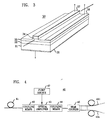
- FIG. 3 schematically shows an electrically pumped device 30 according to the invention.
- a structurally similar device, suitable for intensity modulation of 1.55 ⁇ m radiation, has been disclosed by R. D. Lumble et al., Electronics Letters , Vol. 26 (20), pp. 1653-1655.
- numeral 31 refers to the single crystal Si substrate (exemplarily doped n+); 32 to the epitaxial Si lower cladding layer (exemplarily doped n); 33 to the epitaxial SiGe alloy core layer (exemplarily p-doped Ge 0.2 Si 0.8 ); and 34 to the epitaxial Si top cladding layer (exemplarily doped n).
- Layers 35, 36 and 37 are metal contact layers that facilitate electrical pumping of the device, with consequent amplification of the radiation coupled into the device.
- core layer 33 comprises RE and a co-dopant according to the invention, and optionally comprises oxygen.
- electrically pumped embodiments of the invention do not necessarily involve three-terminal devices as shown in FIG. 3, and that a two-terminal p-n structure also has utility.
- Such a device can be produced by a generally conventional process that is modified to include implantation of the co-dopant or co-dopants.
- FIG. 4 depicts schematically a portion 40 of an exemplary optical fiber transmission system according to the invention, wherein radiation is transmitted from some generation means (not shown) through optical fiber 41 to amplification means that comprise coupling means 42 (comprising, e.g., focusing means such as a spherical lens) that serve to couple the radiation into the appropriately doped core of inventive planar optical amplifier 43.
- coupling means 42 comprising, e.g., focusing means such as a spherical lens
- the radiation is amplified by stimulated emission, the pump energy derived from pump source 47 (typically an electrical power supply).
- Optional coupling means 44 serve to couple the amplified radiation into utilization means, exemplarily star coupler 45 serving to divide the radiation into n outputs that are coupled into n optical fibers 461-46n.
- the signals are transmitted through said fibers to some appropriate utilization means, e.g., an optical detector on a subscriber premise.
- amplification means according to the invention may be utilized in optical computing means.
- devices according to the invention can serve as radiation sources, namely, as lasers or LEDs.
Landscapes
- Engineering & Computer Science (AREA)
- Physics & Mathematics (AREA)
- Manufacturing & Machinery (AREA)
- Electromagnetism (AREA)
- Optics & Photonics (AREA)
- General Physics & Mathematics (AREA)
- Condensed Matter Physics & Semiconductors (AREA)
- Computer Hardware Design (AREA)
- Microelectronics & Electronic Packaging (AREA)
- Power Engineering (AREA)
- Lasers (AREA)
- Semiconductor Lasers (AREA)
- Optical Integrated Circuits (AREA)
- Led Device Packages (AREA)
- Led Devices (AREA)
Abstract
Description
- This invention pertains to the field of optical devices, including opto-electronic devices that utilize spontaneous or stimulated emission of radiation.
- It has long been recognized that it would be highly desirable to have available Si-based lasers, LEDs or optical amplifiers, since availability of these devices would greatly ease the difficulty of integrating optical and electronic functions on a single chip. Furthermore, the high thermal conductivity of Si could result in operational advantages. However, up to now efforts to obtain Si-based LEDs, lasers or amplifiers, especially such devices that operate at commercially interesting wavelengths (e.g., about 1.3 or 1.5 µm) have not been successful.
- H. Ennen et al. [Applied Physics Letters, Vol. 43, page 943 (1983)] pointed out the potential of rare earth (RE) ions in a semiconductor matrix for the development of LED's and lasers. Erbium (Er) is a promising candidate because it shows luminescence in Si at about 1.54 µm, a wavelength of interest for, inter alia, optical fiber communications. See, for instance, H. Ennen et al., Applied Physics Letters, Vol. 46, page 381 (1985). Recently it was observed that the presence of oxygen in Er-doped Si results in increased Er photoluminescence, [P. M. Favennec et al., Japanese Journal of Applied Physics, Vol. 29, page L524, (1990)]. In these studies Er was introduced into Si by implantation, either during MBE growth or in the as-grown substrate. Further background material can be found in U.S. patent 5,039, 190.
- However, despite intense effort and some resultant progress, the art has not yet succeeded in the quest for a Si-based RE-doped LED, laser or optical amplifier, at least in part due to the fact that the observed luminescence is too weak to support such a device. Thus, it would be of substantial interest to discover means for increasing the luminescence from RE-doped Si beyond what can be obtained by the incorporation of oxygen into the Si. This application discloses such means.
- The invention is as defined by the claims, and exemplarily is an article or a system that comprises an optical device, typically a device that utilizes stimulated emission (i.e., a laser or amplifier), but not excluding a light emitting diode (LED). The device according to the invention comprises rare earth (preferably Er, Pr and/or Nd)-doped Si-based planar means adapted for guiding or confining electromagnetic radiation of a predetermined wavelength. Such planar means will herein collectively be referred to as planar waveguide means. The waveguide material exhibits increased luminescence, as compared to the analogous prior art RE-doped Si, including prior art RE-doped Czochraski-grown (CZ) Si.
- More specifically, the waveguide means are adapted for guiding signal radiation of wavelength λs. The gain device also comprises means for causing at least some of the RE in the waveguide means to undergo an electronic transition to an excited electronic state that is associated with luminescence. Exemplarily, said causing means comprise means for coupling pump radiation of wavelength λp < λs into the waveguide means. However, in preferred embodiments, said causing means comprise means for injection of non-equilibrium charge carriers by means of a forward biased p-n junction or other appropriate injection mechanisms, e.g., means that produce impact excitation with hot carriers, or avalanche breakdown.
- The Si-based waveguide material typically contains more than 90 atomic % Si, or Si and Ge, and typically is single crystal material that may be an integral part of a single crystal (doped or undoped) Si body. Significantly, the waveguide material also contains one or more light (atomic number ≦9, but excluding oxygen) elements, preferably C, N, or F, but not excluding Be, herein referred-to as a "co-dopant". The presence of the co-dopant can result in substantially higher luminescence, as compared to analogous prior art material. In currently preferred embodiments the waveguide material further contains oxygen in an amount that is effective to still further increase the luminescence.
- It will be understood that herein the luminescence is always compared between material according to the invention and (comparison) material that is identical to the inventive material except for the absence of the relevant constituent, e.g., the co-dopant or oxygen, as the case may be. We consider an improvement of 10% to be substantial, but typically "substantial" improvements in photoluminescence herein are more than 50% or even more than 100% improvements.
- In currently preferred embodiments of the invention the excitation of the luminescing species (e.g., Er⁺³) involves charge injection. The resulting luminescence thus is electroluminescence, a known phenomenon. Means for electrical "pumping" of waveguide means are known and will typically comprise doping of the waveguide means such that a p-n junction is formed, and will further comprise means for electrically contacting, respectively, the p-portion and the n-portion of the waveguide, such that current can be caused to flow between the contacting means.
-
- FIG. 1 shows experimental data on luminescence from Er-containing Si, co-doped with a variety of elements;
- FIG. 2 schematically depicts an exemplary planar waveguide.
- FIG. 3 schematically shows an exemplary injection-pumped device according to the invention; and
- FIG. 4 schematically shows a relevant portion of a communication system according to the invention.
- A significant aspect of the instant invention is enhancement of RE (typically Er, Pr and/or Nd) luminescence in Si-based waveguides by means of appropriate co-dopants. These rare earths are of special interest since their luminescence spectrum includes wavelengths of particular interest for optical fiber communications, respectively about 1. 54 µm and 1. 3 µm. As is well known, the different RE elements have very similar properties. Thus it can be expected that, in general, a luminescence effect observed with one RE element, e.g., with Er, will also be observed with other RE elements.
- Co-doping can be accomplished by ion implantation into an appropriately shaped Si or Si-containing body. However, other means of co-doping are contemplated, including growth (e.g., by MBE) of appropriately doped Si or SiGe alloy.
- Into conventional Si wafers we implanted Er at energies up to 5.25 MeV. The highest energy, according to standard calculations, locates the maximum Er concentration at about 1.5 µm depth from the wafer surface. We furthermore co-implanted various other elements, the ion energies typically chosen to result in maximum ion concentration at about 1.5 µm depth. After completion of the implantation the wafers were annealed in a vacuum furnace. Some of the Si wafers were Czochralski-grown (CZ) material which is known to contain a significant concentration (up to about 10¹⁸ cm⁻³) of oxygen. The remainder of the Si wafers were float zone (FZ) material, known to contain significantly less oxygen.
- FIG. 1 shows PL data (1.537 µm) for Si samples implanted with Er together with the indicated elements. The speak concentrations of all implanted elements were 10¹⁸ cm⁻³, and all samples were annealed at 900°C for 30 minutes.
Dash line 10 corresponds to PL from Er-doped (CZ) Si, without co-doping, FIG. 1 reveals the surprising and unexpected result that there exist some light elements (including C, N and F, but possibly also Be) whose presence in Er-doped Si can result in greatly increased luminescence. Although a substantial increase is observed in FZ material (seebars bars - The data of FIG. 1 were obtained by exciting PL with 150 mW (corresponding to 100 mW/cm² at the sample) of 488 nm radiation from an argon ion laser, and measuring the luminescence with a 0.75 m commercial monochromator and a cooled Ge detector. The data were obtained at 4.2K. However, the relative intensities are expected to be substantially similar at room temperature.
- As is well known, an optical waveguide comprises a "core" region having a first effective refractive index, the core region being surrounded by a "cladding" region having a second effective refractive index that is lower than the first index. Planar optical waveguides are known, including planar Er-implanted glass waveguides. See, for instance, US patent application Serial No. 07/579,118, incorporated herein by reference.
- Exemplary of waveguide means suitable for use in apparatus according to the invention is a ridge waveguide as is schematically depicted in FIG. 2, wherein numeral 21 refers to the Si substrate, 22 to a core layer (e.g., comprising at least 90 atomic % SiGe alloy having effective refractive index greater than that of Si, and 23 to a cladding layer, e.g., SiO₂ or Si.
Numeral 24 refers to the ridge whose presence provides lateral guiding of the radiation. It will be appreciated that in devices according to the invention at least a portion of layer 22 (typically the portion underlying ridge 24) is doped with the appropriate rare earth ions and the co-dopant or co-dopants. Such an optical waveguide can be produced by known procedures. - A variety of materials systems have been used for planar optical waveguides. Among these is GaAs and related III-V compounds such as AlGaAs. Whereas III-V semiconductors can be used to manufacture optical gain devices, their thermal conductivity typically is relatively low, limiting the pumping energy (radiation or electrical current) that can be dissipated. On the other hand, Si has relatively high thermal conductivity, making it possible to construct relatively long (e.g., of order 1 cm) devices according to the invention. This is expected to, inter alia, facilitate design and manufacture of devices capable of providing significant gain for signal radiation of the wavelength or wavelengths of interest herein.
- FIG. 3 schematically shows an electrically pumped
device 30 according to the invention. A structurally similar device, suitable for intensity modulation of 1.55 µm radiation, has been disclosed by R. D. Laveau et al., Electronics Letters, Vol. 26 (20), pp. 1653-1655. In FIG. 3, numeral 31 refers to the single crystal Si substrate (exemplarily doped n⁺); 32 to the epitaxial Si lower cladding layer (exemplarily doped n); 33 to the epitaxial SiGe alloy core layer (exemplarily p-doped Ge0.2 Si0.8); and 34 to the epitaxial Si top cladding layer (exemplarily doped n).Layers core layer 33 comprises RE and a co-dopant according to the invention, and optionally comprises oxygen. It will also be appreciated that electrically pumped embodiments of the invention do not necessarily involve three-terminal devices as shown in FIG. 3, and that a two-terminal p-n structure also has utility. Such a device can be produced by a generally conventional process that is modified to include implantation of the co-dopant or co-dopants. - FIG. 4 depicts schematically a
portion 40 of an exemplary optical fiber transmission system according to the invention, wherein radiation is transmitted from some generation means (not shown) throughoptical fiber 41 to amplification means that comprise coupling means 42 (comprising, e.g., focusing means such as a spherical lens) that serve to couple the radiation into the appropriately doped core of inventive planaroptical amplifier 43. In 43 the radiation is amplified by stimulated emission, the pump energy derived from pump source 47 (typically an electrical power supply). Optional coupling means 44 serve to couple the amplified radiation into utilization means,exemplarily star coupler 45 serving to divide the radiation into n outputs that are coupled into n optical fibers 461-46n. The signals are transmitted through said fibers to some appropriate utilization means, e.g., an optical detector on a subscriber premise. - Those skilled in the art will appreciate that systems according to the invention can The many forms, and the examples described herein are intended to be illustrative only. For instance, amplification means according to the invention may be utilized in optical computing means. Furthermore, devices according to the invention can serve as radiation sources, namely, as lasers or LEDs.
Claims (10)
- An article or system comprising a device (30) that comprises optical waveguide means (32, 33, 34) adapted for guiding signal radiation of wavelength λs, said waveguide means comprising material that contains a rare earth (RE) element selected from the group consisting of erbium (Er), praseodymium (Pr) and neodymium (Nd), the device further comprising means (35, 36, 37) for causing at least some of the RE in the waveguide means to undergo an electronic transition to an excited electronic state that is associated with luminescence;
CHARACTERIZED IN THATa) the waveguide means are planar waveguide means comprising a core region (33) comprising semiconductor material selected from the group consisting of Si and SiGe alloy; andb) the core region further comprises at least one member of the group of elements consisting of C, N, and F, said member to be referred-to as a the "co-dopant", such that the luminescence associated with the waveguide means is substantially higher than the luminescence associated with otherwise identical comparison waveguide means that do not contain the co-dopant. - The article or system of claim 1, wherein the core region further comprises oxygen in an amount effective to result in increased luminescence, as compared to otherwise identical comparison waveguide means that substantially do not contain oxygen.
- The article or system of claim 1, wherein said at least one of the co-dopants is present in an amount sufficient to result in luminescence intensity that is at least double the luminescence intensity associated with said comparison waveguide means.
- The article or system of claim 1, wherein the optical waveguide means are an integral part of a body that comprises single crystal Si.
- The article or system of claim 4, wherein said means for causing the RE to undergo the transition comprise means for coupling into the core region electromagnetic radiation of wavelength λp < λs.
- The article or system of claim 4, wherein said means for causing the RE to undergo the transition comprise a n-doped and a p-doped portion of the waveguide means, arranged such as to form a p-n junction, and further comprises means for electrically contacting said n-doped portion and said p-doped portion, such that an electrical current can be caused to flow across the p-n junction.
- The article or system of claim 1, wherein the device comprises reflective means adapted for forming an optical cavity for the signal radiation, the device being a laser.
- The article or system of claim 1, further comprising means for coupling the signal radiation into the core region of the waveguide means, and means for providing signal radiation from the waveguide means to radiation utilization means, wherein the device is an optical amplifier.
- The article or system of claim 2, wherein RE is Er, and wherein λs is approximately equal to 1.55 µm.
- The article or system of claim 6, wherein the article comprises a p-n homojunction structure in a light emitting diode configuration.
Applications Claiming Priority (2)
| Application Number | Priority Date | Filing Date | Title |
|---|---|---|---|
| US711243 | 1991-06-06 | ||
| US07/711,243 US5107538A (en) | 1991-06-06 | 1991-06-06 | Optical waveguide system comprising a rare-earth Si-based optical device |
Publications (3)
| Publication Number | Publication Date |
|---|---|
| EP0517440A2 true EP0517440A2 (en) | 1992-12-09 |
| EP0517440A3 EP0517440A3 (en) | 1993-01-20 |
| EP0517440B1 EP0517440B1 (en) | 1994-12-28 |
Family
ID=24857304
Family Applications (1)
| Application Number | Title | Priority Date | Filing Date |
|---|---|---|---|
| EP92304896A Expired - Lifetime EP0517440B1 (en) | 1991-06-06 | 1992-05-29 | Article or system comprising a Si-based optical device |
Country Status (4)
| Country | Link |
|---|---|
| US (1) | US5107538A (en) |
| EP (1) | EP0517440B1 (en) |
| JP (1) | JPH081974B2 (en) |
| DE (1) | DE69201013T2 (en) |
Cited By (7)
| Publication number | Priority date | Publication date | Assignee | Title |
|---|---|---|---|---|
| EP0799495A1 (en) * | 1994-11-10 | 1997-10-08 | Lawrence Semiconductor Research Laboratory, Inc. | Silicon-germanium-carbon compositions and processes thereof |
| EP0945938A2 (en) * | 1998-02-25 | 1999-09-29 | International Business Machines Corporation | Electric pumping of rare-earth-doped silicon for optical emission |
| EP1081812A1 (en) * | 1999-09-02 | 2001-03-07 | STMicroelectronics S.r.l. | Semiconductor device for electro-optic applications, method for manufacturing said device and corresponding semiconductor laser device |
| WO2002013243A2 (en) * | 2000-08-08 | 2002-02-14 | Translucent Photonics, Inc. | Devices with optical gain in silicon |
| EP1196954A1 (en) * | 1999-04-23 | 2002-04-17 | University of Cincinnati | Visible light emitting device formed from wide band gap semiconductor doped with a rare earth element |
| US6570187B1 (en) | 1999-02-10 | 2003-05-27 | Commissariat a l′Energie Atomique | Silicon light-emitting device and method for the production thereof |
| WO2003096437A2 (en) * | 2002-05-06 | 2003-11-20 | Intel Corporation | Silicon and silicon-germanium light-emitting device, methods and systems |
Families Citing this family (67)
| Publication number | Priority date | Publication date | Assignee | Title |
|---|---|---|---|---|
| DE4022090A1 (en) * | 1989-12-18 | 1991-06-20 | Forschungszentrum Juelich Gmbh | ELECTRO-OPTICAL COMPONENT AND METHOD FOR THE PRODUCTION THEREOF |
| DE4011860A1 (en) * | 1990-04-09 | 1991-10-10 | Siemens Ag | SEMICONDUCTOR ELEMENT WITH A SILICON LAYER |
| JP2755471B2 (en) * | 1990-06-29 | 1998-05-20 | 日立電線株式会社 | Rare earth element doped optical waveguide and method of manufacturing the same |
| FR2675592B1 (en) * | 1991-04-22 | 1993-07-16 | Alcatel Nv | OPTICAL AMPLIFIER IN THE SPECTRAL AREA 1.26 TO 1.34 MUM. |
| FR2685135B1 (en) * | 1991-12-16 | 1994-02-04 | Commissariat A Energie Atomique | MINI OPTICALLY PUMPED LASER CAVITY, ITS MANUFACTURING METHOD AND LASER USING THE SAME. |
| US5322813A (en) * | 1992-08-31 | 1994-06-21 | International Business Machines Corporation | Method of making supersaturated rare earth doped semiconductor layers by chemical vapor deposition |
| US5369657A (en) * | 1992-09-15 | 1994-11-29 | Texas Instruments Incorporated | Silicon-based microlaser by doped thin films |
| US5384795A (en) * | 1992-09-15 | 1995-01-24 | Texas Instruments Incorporated | Light emission from rare-earth element-doped CaF2 thin films by electroluminescence |
| JPH06203959A (en) * | 1992-09-30 | 1994-07-22 | Texas Instr Inc <Ti> | Method and apparatus for making nd doped caf2 thin film emit light by electroluminescence |
| US5259046A (en) * | 1992-10-01 | 1993-11-02 | At&T Bell Laboratories | Article comprising an optical waveguide containing a fluorescent dopant |
| JPH087286B2 (en) * | 1992-10-28 | 1996-01-29 | インターナショナル・ビジネス・マシーンズ・コーポレイション | Optical waveguide device |
| DE69315359T2 (en) * | 1993-09-21 | 1998-06-10 | Bookham Technology Ltd | ELECTRO-OPTICAL DEVICE |
| US5491768A (en) * | 1994-07-27 | 1996-02-13 | The Chinese University Of Hong Kong | Optical waveguide employing modified gallium arsenide |
| US5548128A (en) * | 1994-12-14 | 1996-08-20 | The United States Of America As Represented By The Secretary Of The Air Force | Direct-gap germanium-tin multiple-quantum-well electro-optical devices on silicon or germanium substrates |
| US6233070B1 (en) | 1998-05-19 | 2001-05-15 | Bookham Technology Plc | Optical system and method for changing the lengths of optical paths and the phases of light beams |
| US6351578B1 (en) * | 1999-08-06 | 2002-02-26 | Gemfire Corporation | Thermo-optic switch having fast rise-time |
| JP2001135893A (en) | 1999-11-05 | 2001-05-18 | Fujitsu Ltd | Optical semiconductor device and photoelectron integrated circuit device |
| WO2001040540A1 (en) * | 1999-12-02 | 2001-06-07 | Tegal Corporation | Improved reactor with heated and textured electrodes and surfaces |
| US6506289B2 (en) | 2000-08-07 | 2003-01-14 | Symmorphix, Inc. | Planar optical devices and methods for their manufacture |
| US6533907B2 (en) | 2001-01-19 | 2003-03-18 | Symmorphix, Inc. | Method of producing amorphous silicon for hard mask and waveguide applications |
| US7469558B2 (en) * | 2001-07-10 | 2008-12-30 | Springworks, Llc | As-deposited planar optical waveguides with low scattering loss and methods for their manufacture |
| US7404877B2 (en) * | 2001-11-09 | 2008-07-29 | Springworks, Llc | Low temperature zirconia based thermal barrier layer by PVD |
| US7290407B1 (en) | 2001-12-19 | 2007-11-06 | Jesse Chienhua Shan | Triangle-shaped planar optical waveguide having reduced scattering loss |
| US7378356B2 (en) * | 2002-03-16 | 2008-05-27 | Springworks, Llc | Biased pulse DC reactive sputtering of oxide films |
| US20030175142A1 (en) * | 2002-03-16 | 2003-09-18 | Vassiliki Milonopoulou | Rare-earth pre-alloyed PVD targets for dielectric planar applications |
| US6884327B2 (en) * | 2002-03-16 | 2005-04-26 | Tao Pan | Mode size converter for a planar waveguide |
| US20070264564A1 (en) | 2006-03-16 | 2007-11-15 | Infinite Power Solutions, Inc. | Thin film battery on an integrated circuit or circuit board and method thereof |
| US8404376B2 (en) | 2002-08-09 | 2013-03-26 | Infinite Power Solutions, Inc. | Metal film encapsulation |
| US8021778B2 (en) | 2002-08-09 | 2011-09-20 | Infinite Power Solutions, Inc. | Electrochemical apparatus with barrier layer protected substrate |
| US8445130B2 (en) | 2002-08-09 | 2013-05-21 | Infinite Power Solutions, Inc. | Hybrid thin-film battery |
| US8535396B2 (en) | 2002-08-09 | 2013-09-17 | Infinite Power Solutions, Inc. | Electrochemical apparatus with barrier layer protected substrate |
| US8236443B2 (en) | 2002-08-09 | 2012-08-07 | Infinite Power Solutions, Inc. | Metal film encapsulation |
| US8394522B2 (en) | 2002-08-09 | 2013-03-12 | Infinite Power Solutions, Inc. | Robust metal film encapsulation |
| US8431264B2 (en) | 2002-08-09 | 2013-04-30 | Infinite Power Solutions, Inc. | Hybrid thin-film battery |
| WO2004021532A1 (en) * | 2002-08-27 | 2004-03-11 | Symmorphix, Inc. | Optically coupling into highly uniform waveguides |
| WO2004077519A2 (en) | 2003-02-27 | 2004-09-10 | Mukundan Narasimhan | Dielectric barrier layer films |
| US8728285B2 (en) | 2003-05-23 | 2014-05-20 | Demaray, Llc | Transparent conductive oxides |
| US7238628B2 (en) * | 2003-05-23 | 2007-07-03 | Symmorphix, Inc. | Energy conversion and storage films and devices by physical vapor deposition of titanium and titanium oxides and sub-oxides |
| WO2005002006A2 (en) * | 2003-06-30 | 2005-01-06 | University Of Cincinnati | Impurity-based electroluminescent waveguide amplifier and methods for amplifying optical data signals |
| JP2005116709A (en) * | 2003-10-06 | 2005-04-28 | Sony Corp | Semiconductor integrated circuit device and its manufacturing method |
| US7440180B2 (en) * | 2004-02-13 | 2008-10-21 | Tang Yin S | Integration of rare-earth doped amplifiers into semiconductor structures and uses of same |
| JP2006133723A (en) * | 2004-10-08 | 2006-05-25 | Sony Corp | Light guide module and optoelectric hybrid device, and their manufacturing method |
| US7959769B2 (en) | 2004-12-08 | 2011-06-14 | Infinite Power Solutions, Inc. | Deposition of LiCoO2 |
| TWI331634B (en) | 2004-12-08 | 2010-10-11 | Infinite Power Solutions Inc | Deposition of licoo2 |
| WO2006066611A1 (en) * | 2004-12-24 | 2006-06-29 | Pirelli & C. S.P.A. | Photodetector in germanium on silicon |
| US7037806B1 (en) * | 2005-02-09 | 2006-05-02 | Translucent Inc. | Method of fabricating silicon-on-insulator semiconductor substrate using rare earth oxide or rare earth nitride |
| JP2006332137A (en) * | 2005-05-23 | 2006-12-07 | Nippon Telegr & Teleph Corp <Ntt> | Light-emitting device |
| US7838133B2 (en) * | 2005-09-02 | 2010-11-23 | Springworks, Llc | Deposition of perovskite and other compound ceramic films for dielectric applications |
| JP5583344B2 (en) * | 2005-12-09 | 2014-09-03 | セムイクウィップ・インコーポレーテッド | System and method for manufacturing semiconductor devices by implantation of carbon clusters |
| WO2007137157A2 (en) * | 2006-05-18 | 2007-11-29 | Massachusetts Institute Of Technology | Extrinsic gain laser and optical amplification device |
| US8062708B2 (en) | 2006-09-29 | 2011-11-22 | Infinite Power Solutions, Inc. | Masking of and material constraint for depositing battery layers on flexible substrates |
| US8197781B2 (en) | 2006-11-07 | 2012-06-12 | Infinite Power Solutions, Inc. | Sputtering target of Li3PO4 and method for producing same |
| US7919402B2 (en) * | 2006-12-06 | 2011-04-05 | Semequip, Inc. | Cluster ion implantation for defect engineering |
| US8144392B2 (en) * | 2007-02-12 | 2012-03-27 | The United States Of America As Represented By The Secretary Of The Navy | Waveguide amplifier in a sputtered film of erbium-doped gallium lanthanum sulfide glass |
| WO2008128039A2 (en) * | 2007-04-11 | 2008-10-23 | Semequip, Inc. | Cluster ion implantation for defect engineering |
| US8268488B2 (en) | 2007-12-21 | 2012-09-18 | Infinite Power Solutions, Inc. | Thin film electrolyte for thin film batteries |
| KR20100102180A (en) | 2007-12-21 | 2010-09-20 | 인피니트 파워 솔루션스, 인크. | Method for sputter targets for electrolyte films |
| KR101606183B1 (en) | 2008-01-11 | 2016-03-25 | 사푸라스트 리써치 엘엘씨 | Thin film encapsulation for thin film batteries and other devices |
| EP2266183B1 (en) | 2008-04-02 | 2018-12-12 | Sapurast Research LLC | Passive over/under voltage control and protection for energy storage devices associated with energy harvesting |
| EP2319101B1 (en) * | 2008-08-11 | 2015-11-04 | Sapurast Research LLC | Energy device with integral collector surface for electromagnetic energy harvesting and method thereof |
| CN102150185B (en) | 2008-09-12 | 2014-05-28 | 无穷动力解决方案股份有限公司 | Energy device with integral conductive surface for data communication via electromagnetic energy and method thereof |
| WO2010042594A1 (en) | 2008-10-08 | 2010-04-15 | Infinite Power Solutions, Inc. | Environmentally-powered wireless sensor module |
| KR101792287B1 (en) | 2009-09-01 | 2017-10-31 | 사푸라스트 리써치 엘엘씨 | Printed circuit board with integrated thin film battery |
| US20110300432A1 (en) | 2010-06-07 | 2011-12-08 | Snyder Shawn W | Rechargeable, High-Density Electrochemical Device |
| JP5831165B2 (en) | 2011-11-21 | 2015-12-09 | 富士通株式会社 | Semiconductor optical device |
| CN103219646A (en) * | 2013-03-21 | 2013-07-24 | 常州镭赛科技有限公司 | Light amplifier |
| CN110429474B (en) * | 2019-07-31 | 2021-05-14 | 天津工业大学 | All-four-group silicon-based C-band semiconductor laser |
Citations (2)
| Publication number | Priority date | Publication date | Assignee | Title |
|---|---|---|---|---|
| DE3319134A1 (en) * | 1983-05-26 | 1985-05-02 | Fraunhofer-Gesellschaft zur Förderung der angewandten Forschung e.V., 8000 München | Optoelectronic component, in particular a laser diode or a light-emitting diode |
| JPH03100528A (en) * | 1989-09-13 | 1991-04-25 | Hitachi Cable Ltd | Active transmission line for plural wavelength transmission and transmission system using the same |
Family Cites Families (10)
| Publication number | Priority date | Publication date | Assignee | Title |
|---|---|---|---|---|
| JPS60114811A (en) * | 1983-11-28 | 1985-06-21 | Hitachi Ltd | Optical waveguide and its production |
| US4575919A (en) * | 1984-05-24 | 1986-03-18 | At&T Bell Laboratories | Method of making heteroepitaxial ridge overgrown laser |
| GB8724736D0 (en) * | 1987-10-22 | 1987-11-25 | British Telecomm | Optical fibre |
| US5023885A (en) * | 1988-09-20 | 1991-06-11 | Siemens Aktiengesellschaft | External optical resonator for a semiconductor laser |
| US4962995A (en) * | 1989-06-16 | 1990-10-16 | Gte Laboratories Incorporated | Glasses for high efficiency erbium (3+) optical fiber lasers, amplifiers, and superluminescent sources |
| JPH0373934A (en) * | 1989-08-15 | 1991-03-28 | Fujitsu Ltd | Optical amplifier |
| US5005175A (en) * | 1989-11-27 | 1991-04-02 | At&T Bell Laboratories | Erbium-doped fiber amplifier |
| US5027079A (en) * | 1990-01-19 | 1991-06-25 | At&T Bell Laboratories | Erbium-doped fiber amplifier |
| JPH0644645B2 (en) * | 1990-03-30 | 1994-06-08 | ホーヤ株式会社 | Optical waveguide type laser medium and optical waveguide type laser device |
| US5039190A (en) * | 1990-09-07 | 1991-08-13 | At&T Bell Laboratories | Apparatus comprising an optical gain device, and method of producing the device |
-
1991
- 1991-06-06 US US07/711,243 patent/US5107538A/en not_active Expired - Lifetime
-
1992
- 1992-05-11 JP JP14364492A patent/JPH081974B2/en not_active Expired - Lifetime
- 1992-05-29 EP EP92304896A patent/EP0517440B1/en not_active Expired - Lifetime
- 1992-05-29 DE DE69201013T patent/DE69201013T2/en not_active Expired - Fee Related
Patent Citations (2)
| Publication number | Priority date | Publication date | Assignee | Title |
|---|---|---|---|---|
| DE3319134A1 (en) * | 1983-05-26 | 1985-05-02 | Fraunhofer-Gesellschaft zur Förderung der angewandten Forschung e.V., 8000 München | Optoelectronic component, in particular a laser diode or a light-emitting diode |
| JPH03100528A (en) * | 1989-09-13 | 1991-04-25 | Hitachi Cable Ltd | Active transmission line for plural wavelength transmission and transmission system using the same |
Non-Patent Citations (7)
| Title |
|---|
| APPLIED PHYSICS LETTERS vol. 51, no. 19, 9 November 1987, NEW YORK, USA pages 1509 - 1511 L.T. CANHAM ET AL. '1.3 um light-emitting diode from silicon electron irradiated at its damage threshold' * |
| JAPANESE JOURNAL OF APPLIED PHYSICS vol. 15, no. 3, March 1976, TOKYO, JAPAN pages 567 - 568 S. GONDA ET AL. 'Laser Emission in Nitrogen-Implanted GaAs(1-x)P(x) (x=0.36 and 0.43)' * |
| JAPANESE JOURNAL OF APPLIED PHYSICS vol. 29, no. 4, April 1990, TOKYO, JAPAN pages L524 - L526 P.N. FAVENNEC ET AL. 'Optical Activation of Er(3+) Implanted in Silicon by Oxygen Impurities' * |
| MATERIALS SCIENCE AND ENGINEERING B vol. B4, no. 1/4, October 1989, LAUSANNE, CH pages 95 - 99 , XP95486 L.T. CANHAM 'A Study of Carbon-implanted Silicon for Light-emitting Diode Fabrication' * |
| PATENT ABSTRACTS OF JAPAN vol. 15, no. 292 (P-1230)24 July 1991 * |
| PATENT ABSTRACTS OF JAPAN vol. 15, no. 292 (P-1230)24 July 1991 & JP-A-3 100 528 * |
| PHYSICAL REVIEW B, CONDENSED MATTER vol. 33, no. 2, January 1986, RIDGE, USA pages 1495 - 1498 A. D\RNEN ET AL. 'Nitrogen-crabon radiative defect at 0.746 eV in silicon' * |
Cited By (21)
| Publication number | Priority date | Publication date | Assignee | Title |
|---|---|---|---|---|
| EP0799495A4 (en) * | 1994-11-10 | 1999-11-03 | Lawrence Semiconductor Researc | Silicon-germanium-carbon compositions and processes thereof |
| EP0799495A1 (en) * | 1994-11-10 | 1997-10-08 | Lawrence Semiconductor Research Laboratory, Inc. | Silicon-germanium-carbon compositions and processes thereof |
| EP0945938A3 (en) * | 1998-02-25 | 2001-07-25 | International Business Machines Corporation | Electric pumping of rare-earth-doped silicon for optical emission |
| EP0945938A2 (en) * | 1998-02-25 | 1999-09-29 | International Business Machines Corporation | Electric pumping of rare-earth-doped silicon for optical emission |
| KR100377716B1 (en) * | 1998-02-25 | 2003-03-26 | 인터내셔널 비지네스 머신즈 코포레이션 | Electric pumping of rare-earth-doped silicon for optical emission |
| US6570187B1 (en) | 1999-02-10 | 2003-05-27 | Commissariat a l′Energie Atomique | Silicon light-emitting device and method for the production thereof |
| EP1196954A1 (en) * | 1999-04-23 | 2002-04-17 | University of Cincinnati | Visible light emitting device formed from wide band gap semiconductor doped with a rare earth element |
| EP1196954A4 (en) * | 1999-04-23 | 2006-10-04 | Univ Cincinnati | Visible light emitting device formed from wide band gap semiconductor doped with a rare earth element |
| US6828598B1 (en) | 1999-09-02 | 2004-12-07 | Stmicroelectronics S.R.L. | Semiconductor device for electro-optic applications, method for manufacturing said device and corresponding semiconductor laser device |
| WO2001017074A1 (en) * | 1999-09-02 | 2001-03-08 | Stmicroelectronics S.R.L. | Semiconductor device for electro-optic applications, method for manufacturing said device and corresponding semiconductor laser device |
| EP1081812A1 (en) * | 1999-09-02 | 2001-03-07 | STMicroelectronics S.r.l. | Semiconductor device for electro-optic applications, method for manufacturing said device and corresponding semiconductor laser device |
| US6858864B2 (en) | 2000-08-08 | 2005-02-22 | Translucent Photonics, Inc. | Devices with optical gain in silicon |
| US6734453B2 (en) | 2000-08-08 | 2004-05-11 | Translucent Photonics, Inc. | Devices with optical gain in silicon |
| WO2002013243A2 (en) * | 2000-08-08 | 2002-02-14 | Translucent Photonics, Inc. | Devices with optical gain in silicon |
| WO2002013243A3 (en) * | 2000-08-08 | 2003-03-13 | Translucent Photonics Inc | Devices with optical gain in silicon |
| US7135699B1 (en) | 2000-08-08 | 2006-11-14 | Translucent Photonics, Inc. | Method and apparatus for growth of single-crystal rare-earth oxides, nitrides, and phosphides |
| US7211821B2 (en) | 2000-08-08 | 2007-05-01 | Translucent Photonics, Inc. | Devices with optical gain in silicon |
| WO2003096437A3 (en) * | 2002-05-06 | 2004-02-05 | Intel Corp | Silicon and silicon-germanium light-emitting device, methods and systems |
| WO2003096437A2 (en) * | 2002-05-06 | 2003-11-20 | Intel Corporation | Silicon and silicon-germanium light-emitting device, methods and systems |
| US6924510B2 (en) | 2002-05-06 | 2005-08-02 | Intel Corporation | Silicon and silicon/germanium light-emitting device, methods and systems |
| US7169631B2 (en) | 2002-05-06 | 2007-01-30 | Intel Corporation | Silicon and silicon/germanium light-emitting device, methods and systems |
Also Published As
| Publication number | Publication date |
|---|---|
| EP0517440B1 (en) | 1994-12-28 |
| US5107538A (en) | 1992-04-21 |
| JPH05175592A (en) | 1993-07-13 |
| DE69201013T2 (en) | 1995-05-11 |
| DE69201013D1 (en) | 1995-02-09 |
| EP0517440A3 (en) | 1993-01-20 |
| JPH081974B2 (en) | 1996-01-10 |
Similar Documents
| Publication | Publication Date | Title |
|---|---|---|
| EP0517440B1 (en) | Article or system comprising a Si-based optical device | |
| Thaik et al. | Photoluminescence spectroscopy of erbium implanted gallium nitride | |
| Kenyon | Recent developments in rare-earth doped materials for optoelectronics | |
| Wilson et al. | 1.54‐μm photoluminescence from Er‐implanted GaN and AlN | |
| Kenyon | Erbium in silicon | |
| US5077143A (en) | Silicon electroluminescent device | |
| EP0261875B1 (en) | Rare earth doped semiconductor laser | |
| Jantsch et al. | Different Er centres in Si and their use for electroluminescent devices | |
| US6570187B1 (en) | Silicon light-emitting device and method for the production thereof | |
| EP1210752B1 (en) | Semiconductor laser device for electro-optic applications and method for manufacturing said device | |
| CN112072469A (en) | Semiconductor laser based on quantum well mixed active region and preparation method | |
| CN101557074A (en) | Silica-based germanium electrical injection laser and production method thereof | |
| Reed et al. | Erbium-doped silicon and porous silicon for optoelectronics | |
| McFarlane et al. | Rare earth doped fluoride waveguides fabricated using molecular beam epitaxy | |
| KR100377716B1 (en) | Electric pumping of rare-earth-doped silicon for optical emission | |
| EP0470372A2 (en) | Atomic element doped semi-conductor injection laser fabricated by using ion implantation and epitaxial growth on the implanted surface | |
| US4821274A (en) | Electro-optical semiconductor device and a method of emitting light | |
| Priolo et al. | Optical doping of materials by erbium ion implantation | |
| Zhou et al. | Room-temperature 2 μm luminescence from Tm doped silicon light emitting diodes and SOI substrates | |
| Jantsch et al. | Status, Hopes and Limitations for the Si: Er-based 1.54 μm Emitter | |
| Pearton et al. | Er-doping of gan and related alloys | |
| Chelnokov et al. | Deep erbium-ytterbium implantation codoping of low-loss silicon oxynitride waveguides | |
| Shiryaev et al. | Development of mid-IR chalcogenide fiber emitters | |
| Zavada et al. | Near infrared photonic devices based on Er-doped GaN and InGaN | |
| Peaker | Erbium in semiconductors: where are we coming from; where are we going? |
Legal Events
| Date | Code | Title | Description |
|---|---|---|---|
| PUAI | Public reference made under article 153(3) epc to a published international application that has entered the european phase |
Free format text: ORIGINAL CODE: 0009012 |
|
| PUAL | Search report despatched |
Free format text: ORIGINAL CODE: 0009013 |
|
| AK | Designated contracting states |
Kind code of ref document: A2 Designated state(s): DE FR GB |
|
| AK | Designated contracting states |
Kind code of ref document: A3 Designated state(s): DE FR GB |
|
| 17P | Request for examination filed |
Effective date: 19930708 |
|
| 17Q | First examination report despatched |
Effective date: 19940124 |
|
| RAP3 | Party data changed (applicant data changed or rights of an application transferred) |
Owner name: AT&T CORP. |
|
| GRAA | (expected) grant |
Free format text: ORIGINAL CODE: 0009210 |
|
| AK | Designated contracting states |
Kind code of ref document: B1 Designated state(s): DE FR GB |
|
| REF | Corresponds to: |
Ref document number: 69201013 Country of ref document: DE Date of ref document: 19950209 |
|
| ET | Fr: translation filed | ||
| PLBE | No opposition filed within time limit |
Free format text: ORIGINAL CODE: 0009261 |
|
| STAA | Information on the status of an ep patent application or granted ep patent |
Free format text: STATUS: NO OPPOSITION FILED WITHIN TIME LIMIT |
|
| 26N | No opposition filed | ||
| REG | Reference to a national code |
Ref country code: GB Ref legal event code: IF02 |
|
| PGFP | Annual fee paid to national office [announced via postgrant information from national office to epo] |
Ref country code: FR Payment date: 20090513 Year of fee payment: 18 Ref country code: DE Payment date: 20090525 Year of fee payment: 18 |
|
| PGFP | Annual fee paid to national office [announced via postgrant information from national office to epo] |
Ref country code: GB Payment date: 20090522 Year of fee payment: 18 |
|
| GBPC | Gb: european patent ceased through non-payment of renewal fee |
Effective date: 20100529 |
|
| REG | Reference to a national code |
Ref country code: FR Ref legal event code: ST Effective date: 20110131 |
|
| PG25 | Lapsed in a contracting state [announced via postgrant information from national office to epo] |
Ref country code: DE Free format text: LAPSE BECAUSE OF NON-PAYMENT OF DUE FEES Effective date: 20101201 |
|
| PG25 | Lapsed in a contracting state [announced via postgrant information from national office to epo] |
Ref country code: FR Free format text: LAPSE BECAUSE OF NON-PAYMENT OF DUE FEES Effective date: 20100531 |
|
| PG25 | Lapsed in a contracting state [announced via postgrant information from national office to epo] |
Ref country code: GB Free format text: LAPSE BECAUSE OF NON-PAYMENT OF DUE FEES Effective date: 20100529 |