EP0499706B1 - A transmitting and receiving part of a pulse doppler radar - Google Patents
A transmitting and receiving part of a pulse doppler radar Download PDFInfo
- Publication number
- EP0499706B1 EP0499706B1 EP91121141A EP91121141A EP0499706B1 EP 0499706 B1 EP0499706 B1 EP 0499706B1 EP 91121141 A EP91121141 A EP 91121141A EP 91121141 A EP91121141 A EP 91121141A EP 0499706 B1 EP0499706 B1 EP 0499706B1
- Authority
- EP
- European Patent Office
- Prior art keywords
- frequency
- signal
- arrangement according
- oscillator
- pulse
- Prior art date
- Legal status (The legal status is an assumption and is not a legal conclusion. Google has not performed a legal analysis and makes no representation as to the accuracy of the status listed.)
- Expired - Lifetime
Links
Images


Classifications
-
- G—PHYSICS
- G01—MEASURING; TESTING
- G01S—RADIO DIRECTION-FINDING; RADIO NAVIGATION; DETERMINING DISTANCE OR VELOCITY BY USE OF RADIO WAVES; LOCATING OR PRESENCE-DETECTING BY USE OF THE REFLECTION OR RERADIATION OF RADIO WAVES; ANALOGOUS ARRANGEMENTS USING OTHER WAVES
- G01S7/00—Details of systems according to groups G01S13/00, G01S15/00, G01S17/00
- G01S7/02—Details of systems according to groups G01S13/00, G01S15/00, G01S17/00 of systems according to group G01S13/00
- G01S7/023—Interference mitigation, e.g. reducing or avoiding non-intentional interference with other HF-transmitters, base station transmitters for mobile communication or other radar systems, e.g. using electro-magnetic interference [EMI] reduction techniques
- G01S7/0234—Avoidance by code multiplex
-
- G—PHYSICS
- G01—MEASURING; TESTING
- G01S—RADIO DIRECTION-FINDING; RADIO NAVIGATION; DETERMINING DISTANCE OR VELOCITY BY USE OF RADIO WAVES; LOCATING OR PRESENCE-DETECTING BY USE OF THE REFLECTION OR RERADIATION OF RADIO WAVES; ANALOGOUS ARRANGEMENTS USING OTHER WAVES
- G01S7/00—Details of systems according to groups G01S13/00, G01S15/00, G01S17/00
- G01S7/02—Details of systems according to groups G01S13/00, G01S15/00, G01S17/00 of systems according to group G01S13/00
- G01S7/023—Interference mitigation, e.g. reducing or avoiding non-intentional interference with other HF-transmitters, base station transmitters for mobile communication or other radar systems, e.g. using electro-magnetic interference [EMI] reduction techniques
- G01S7/0235—Avoidance by time multiplex
-
- G—PHYSICS
- G01—MEASURING; TESTING
- G01S—RADIO DIRECTION-FINDING; RADIO NAVIGATION; DETERMINING DISTANCE OR VELOCITY BY USE OF RADIO WAVES; LOCATING OR PRESENCE-DETECTING BY USE OF THE REFLECTION OR RERADIATION OF RADIO WAVES; ANALOGOUS ARRANGEMENTS USING OTHER WAVES
- G01S7/00—Details of systems according to groups G01S13/00, G01S15/00, G01S17/00
- G01S7/02—Details of systems according to groups G01S13/00, G01S15/00, G01S17/00 of systems according to group G01S13/00
- G01S7/03—Details of HF subsystems specially adapted therefor, e.g. common to transmitter and receiver
Definitions
- the present invention relates to a transmitting and receiving part of a pulse Doppler radar having a transmitting oscillator which, with a pulse repetition frequency generates radar pulses of a duration period, and an antenna coupled to the transmitting oscillator.
- a reception mixer is coupled to the antenna and generates intermediate frequencies, and there are means for generating an intermediate-frequency reference frequency.
- Pulse radar systems which are suitable for generating Doppler signals require a detection device in which the phase and the frequency of the transmitted signal are used as references.
- phase-sensitive detector at the outlet of an intermediate frequency amplifier.
- the generating of the phase-stable intermediate-frequency reference signal requires significant equipment expenditures [coherent frequency generating system (M.I. Skolnik; Introduction to Radar Systems; McGraw Hill Publishing Company)].
- the EP-0 154 054 describes a HF arrangement for coherent pulse radar, comprising a transmitting oscillator and a separate stable local oscillator.
- the pulse repetition frequency is generated coherently to a intermediate-frequency reference frequency.
- the US-3 987 442 disloses a digital radar system that comprises in phase mixers and quadrature phase mixers to generate I-signals and Q-signals.
- An object of the present invention is to provide a coherently operating transmitting and receiving part for a pulse Doppler radar which generates Doppler signals from the lowest to the highest Doppler frequencies and produces high-resolution range gates (in the meter range).
- a transmitting and receiving part of a pulse Doppler radar having a transmitting oscillator which, with a pulse repetition frequency generates radar pulses of a duration period, and an antenna coupled to the transmitting oscillator.
- a reception mixer is coupled to the antenna and generates intermediate frequencies, and there are means for generating an intermediate-frequency reference frequency.
- An inphase mixer generates I-signals, and a quadrature phase mixer generates Q-signals.
- the transmitting oscillator is, by means of frequency shifting, used at the same time as the local oscillator.
- the intermediate-frequency reference frequency f r is generated coherently with respect to the pulse repetition frequency f p .
- the radar according to the present invention has an elegant construction and requires only one high-frequency transmitting oscillator. Only moderate demands are made on spectral purity and frequency constancy of this transmitting oscillator. It is therefore possible to use an oscillator with a low-quality resonator. An expensive oscillator with an echo box is not necessary.
- the transmitting and receiving circuit is therefore suitable for complete monolithic integration (MMIC). For this reason, the transmitting and receiving part according to the invention can be used as a radar front end for applications in which only little space is available such as in missiles or aircraft or in motor vehicles for range or distance measuring or for observing rear traffic.
- decorrelating can be achieved of disturbing interference signals of common-channel radio services (in particular, by similar radars).
- Figure 1 is a block diagram of an embodiment of a transmitting and receiving part according to the present invention.
- Figure 2 is an illustration of several signal courses.
- Figure 3 shows a block diagram of a phase-lock loop circuit that produces an intermediate reference frequency from a clock signal used in an embodiment of the present invention.
- Figure 4a is a block diagram of a device, constructed in accordance with an embodiment of the present invention, for coupling a delayed signal to obtain an IF-reference signal pulse.
- Figure 4b is a block diagram of an arrangement for coupling a high Q RF-resonator to an antenna line, constructed in accordance with an embodiment of the present invention.
- Figure 5 is a block diagram of a device for transferring an intermediate-frequency pulse reference signal to a continuous intermediate-frequency reference signal, constructed in accordance with an embodiment of the present invention.
- Figure 6 is a block diagram of a device for generating a continuous intermediate-frequency reference signal by means of a pulsed phase-lock-loop circuit, constructed in accordance with an embodiment of the present invention.
- Figure 7 is a block diagram of a frequency-control for stabilizing a frequency shift sweep, constructed in accordance with an embodiment of the present invention.
- FIG. 8 is a block diagram of a pseudo noise (PN) generation device, constructed in accordance with an embodiment of the present invention.
- PN pseudo noise
- Figure 9 is a schematic of a circuit constructed in accordance with an embodiment of the present invention which limits interfering IF-pulses.
- Figure 10 is a block diagram of a device for generating a staggered pulse repetition frequency, constructed in accordance with an embodiment of the present invention.
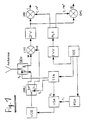
- Figure 1 shows a transmitting and receiving part with the components comprising a transmitting oscillator VCO (Voltage Controlled Oscillator), the pulses of which reach the antenna via an antenna / mixer change-over switch AMU and a transmission/reception change-over switch SEU.
- the echo signals received by the antenna are guided to a reception mixer EMI by the transmission/reception change-over switch SEU. There, they are mixed with the reference frequency LO (of the local oscillator, normally generated by the receiving oscillator) to form the intermediate frequency.
- the intermediate frequency amplifier ZFV the signals reach the inphase mixer IMI and the quadrature phase mixer QMI, from where they are guided to a digital or analog analysis device, which is not a part of the invention.
- a common timing oscillator TOS is provided in the illustrated embodiment from which both signals are derived.
- a shift of the transmitting oscillator VCO takes place by the modulation signal processing device MSA and the bias voltage processing device VSA.
- the control of the antenna/mixer change-over switch AMU and of the transmission/reception change-over switch SEU takes place by a switching timing processing device STA.
- the intermediate-frequency reference frequency f r is derived from the timing oscillator TOS by means of the frequency multiplier FVV.
- the phase output divider PLT transmits the reference signal for the inphase f r /0° and for the quadrature phase f r /90° to the mixers IMI and QMI.
- the oscillator VCO may, for example, be a Gunn element oscillator, the frequency of which can be modulated by means of a varactor diode.
- the required signal paths from the transmitter to the antenna, from the antenna to the LO mixer inlet, and from the antenna to the RF mixer inlet are changed over by the change-over switches AMU and SEU in time with the repetition frequency f p .
- the switches AMU and SEU may be semiconductor switches (preferably gallium arsenide FET) which can be manufactured in MMIC technology to be fast switching and to have a sufficiently high insulation.
- An alternative solution which is not shown illustrated, are configurations which use one coupler and circulator, two couplers, or one coupler and one change-over switch. Between the VCO and the EMI, one coupler and one circulator (in front of the antenna) or two couplers can therefore replace the components AMU and SEU. The first coupler will then, in each case, provide the mixer EMI with the frequency f LO and the coupler or the circulator at the antenna with the frequency f s .
- These alternatives have the advantage of a purely passive solution and do not require any switching signals. Disadvantages are higher signal losses and the inferior insulation of the undesirable signal paths.
- the switching signals s 1 and s 2 and the shift signal p 1 are derived from the central timing oscillator TOS.
- a radar unit receives an intermediate-frequency echo pulse signal from a fixed target that is assumed to be punctiform.
- the echo pulse signal consists of few periods when the transmitted pulse duration t s is only slightly larger than the intermediate-frequency period duration.
- This intermediate-frequency echo pulse signal has the characteristic that it is coherent with the pulse repetition frequency f p irrespective of the carrier phase of the transmitting oscillator VCO at the point in time of the shift. This coherence is utilized for obtaining pulse Doppler signals from moving targets in the base band.
- an intermediate-frequency reference signal f r /0° and f r /90° is supplied to the I- and Q-mixers IMI and QMI for a homodyne beat, this reference signal, being coherent with the pulse repetition frequency f p .
- this coherence can be achieved in that the frequency f p and the reference frequency f r are derived from a common timing oscillator (TOS).
- TOS common timing oscillator
- a frequency multiplier FVV is illustrated as a possible solution which multiplies the timing oscillator frequency to the intermediate-frequency reference frequency f r .
- the reference frequency f r is supplied to the mixers IMI and QMI.
- the reference frequency f r may also be obtained from a delayed signal portion of the transmitted pulse which is received at the beginning of the echo reception time t e at the IF-outlet of the reception mixer EMI.
- the delayed signal portion of the transmitted pulse either the virtually always existing antenna echo signal may be used, or a signal portion is transferred in a defined manner from the transmission path into the reception path by means of two couplers and a delay line.
- the mixer output signals I and Q comprise bipolar video pulses of a pulse width t s with the pulse repetition frequency f p . In a known manner, they are processed in an analog or digital manner as pulse Doppler video signals.
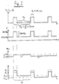
- Figure 2 shows several signal courses.
- Figure 2 shows the switching signals s 1 , s 2 and p 1 by which the components AMU, SEU and, by means of the VSA, also the VCO of Figure 1 are controlled.
- a pulse has, for example, the pulse duration period t s of 30 nsec which corresponds to the transmitted pulse duration period.
- Such pulses are emitted with the pulse repetition frequency f p .
- the duration period to the next pulse t p is approximately 1 ⁇ sec.
- the pulse repetition frequency f p in this case is at 1 MHz.
- the second diagram shows the frequency of the transmitted pulse f s going to the antenna and the beat frequency f LO .
- the transmission takes place, for example, for 30 nsec at 50 GHz.
- the reception takes place for the duration period t e to the next pulse after the change-over to f LO of 49.7 GHz.
- the pulse echo with the frequency 50 GHz therefore comes from the antenna at a time in which the transmitting oscillator VCO has already shifted again to 49.7 GHz.
- the echo signal in the reception mixer EMI is mixed with the LO frequency of 49.7 GHz, in which case the ZF mixed product of approximately 300 MHz is filtered out and further amplified (intermediate-frequency amplifier ZFV) and the signal of which is supplied in a parallel manner to the mixers IMI and QMI.
- ZFV intermediate-frequency amplifier
- the bipolar video signals I and Q Coherence is obtained from the derivation of the reference signals, and also from the timing oscillator TOS.
- the TOS operates, for example, with 25 MHZ, and the frequency multiplier FVV multiplies this frequency by twelve, 300 MHz are obtained, corresponding to the IF-frequency.
- the elements FVV and PLT, as well as other elements of the system, have a constant and arbitrary phase angle. Time-related phase variations which are small with respect to the lowest Doppler frequency do not interfere.
- the initially mentioned requirement of the radar process of offering interference resistance against common-channel interference sources can be met by three measures which may be applied individually or at the same time.
- the first is noise modulation or pseudo noise modulation of the phase or frequency of the transmission oscillator VCO.
- the second is pseudo noise modulation of the pulse repetition frequency f p .
- the third measure is amplitude limitation of individual interference pulses which may occur on an individual basis in a statistically distributed manner in spite of the first two measures mentioned above.
- a received interference signal is decorrelated already in the reception mixer EMI, and the remaining interference energy is suppressed by Doppler signal filtering.
- the frequency modulation of the VCO has the advantage that no additional phase modulator must be used.
- the two lower diagrams of Figure 2 show a possible frequency modulation with the binary modulation signal m 1 .
- This is generated in the modulation voltage processing device MSA by a (pseudo) random generator which is timed with the pulse repetition frequency f p . It is synchronous with the frequency shift signal p 1 and is added to it in the bias voltage processing system VSA.
- the frequency shift f s ' - f s - f' LO - f LO which is caused by the binary modulation signal m 1 , is adjusted in such a manner that in the case of the logic "1", the pertaining phase swing, after the period duration t p , reaches the value 180°. In the case of the logic "0", the frequency sweep (and the phase swing) is zero.
- a (pseudo) noise signal can also be used which is stepped several times in the amplitude (corresponding to the frequency sweep) or which is continuous, on the condition that the respective amplitude step for the period duration t p remains constant and the maximal resulting phase swing has the value of approximately 360°.
- the second measure falls under the term "staggered pulse repetition frequency" and is carried out as follows.
- a number of staggered pulse period durations is provided which, controlled by a pseudo random generator, are called from one pulse to the next.
- the selection of parameters takes place on the condition that: a mean pulse repetition frequency is maintained; the grading of the pulse repetition frequencies corresponds to a range gate width; and a distribution of an interference signal energy to all range gates takes place that is as uniform as possible.
- the third measure provides that interference signal pulses, which clearly exceed the level of the useful-signal pulses, are cut off by an amplitude limiting in the ZF-amplifier chain.
- the interference pulses can occur only relatively infrequently and in an isolated manner but with a very high amplitude.
- the amplitude limiting is therefore the appropriate device for the suppressing of interference signals while the useful signal loss is low.
- FIG 3 illustrates an embodiment of a phase-lock-loop circuit that produces an intermediate reference frequency fr from the clock signal of the timing oscillator TOS of Figure 1.
- This phase-lock-loop circuit can be used instead of the frequency multiplier FVV of Figure 1, and includes a sampling pulse generator coupled to the timing oscillator TOS.
- a sampling phase detector is coupled to the sampling pulse generator, a loop filter, followed by a voltage controlled oscillator are coupled to the sampling phase detector.
- the output of the voltage controlled oscillator is provided to the phase output divider PLT.
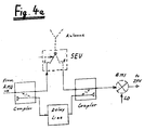
- Figure 4a illustrates a block diagram of a device that couples a delayed signal portion of the transmitted pulse into the reception path in order to obtain an IF-reference signal pulse.
- the device includes a first coupler connected to the antenna/mixer change-over switch AMU and the switch SEU, a second coupler connected between the switch SEU and the reception mixer EMI, and a delay line connected between the first and second couplers.
- Figure 4b is a block diagram of an arrangement that couples a high Q RF-resonator to the antenna line, that can be used with the embodiment of Figure 1.
- the arrangement includes a coupler connected between the switch SEU and the antenna, this coupler also being connected to the RF-resonator.
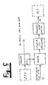
- FIG. 5 is a block diagram of a device for transforming the intermediate-frequency pulse reference signal to a continuous intermediate-frequency reference signal.
- This device includes a gate connected to the switching timing processing device STA, and a coupler connected to the output of the intermediate frequency amplifier ZFV and to the gate.
- the output of the gate is provided to a high Q IF-resonator, which is connected to an amplifier and limiter.
- the phase output divider PLT receives the intermediate-frequency reference signal fr from the amplifier and limiter.
- Figure 6 shows another embodiment of a device for generating a continuous intermediate-frequency reference signal.
- a gate receives a gated pulse fp from the device STA.
- the gate is coupled via a coupler to the intermediate frequency amplifier ZFV, with the output of the gate being connected to a pulsed phase detector.
- the pulsed phase detector along with a sample and hold filter and a voltage controlled oscillator VCO, form a pulsed phase-lock-loop circuit that is provides the intermediate-frequency reference signal to the phase output divider PLT.
- FIG 7 is a block diagram of a frequency control device for stabilizing the frequency shift sweep D by locking it to the intermediate frequency reference signal fr which is derived from the timing oscillator TOS by the frequency multiplier FVV.
- the frequency control device includes an intermediate frequency reference signal generator, such as that shown in Figures 5 and 6. The generator provides the fr signal to a phase detector. A frequency or phase difference between the frequency shift sweep D and the reference frequency signal derived from the timing oscillator via the frequency divider FVV creates an appropriate control voltage at the output of the phase detector. This control voltage adjusts the frequency shift sweep D in the VCO via a PLL-filter and a bias voltage processing device VSA.
- Figure 8 is a block diagram of a pseudo noise (PN) generation device for frequency modulation of the transmission oscillator VCO as shown by the signal courses of Figure 2.
- PN pseudo noise
- Figure 9 is a schematic circuit for limiting IF-pulses which exceed a given amplitude threshold. This circuit is coupled at the end of the linear IF amplifier chain ZFV and before the mixers IMI and QMI.
- Figure 10 is a block diagram of a device for generating a staggered pulse repetition frequency by means of a pseudo noise generator (PN) such as that shown in Figure 8 and a programmable frequency divider.
- PN pseudo noise generator
- the programmable divider with pseudo noise generator is coupled between the timing oscillator TOS and the switching timing processing device STA and the modulation signal processing device MSA.
Landscapes
- Engineering & Computer Science (AREA)
- Computer Networks & Wireless Communication (AREA)
- Radar, Positioning & Navigation (AREA)
- Remote Sensing (AREA)
- Physics & Mathematics (AREA)
- General Physics & Mathematics (AREA)
- Radar Systems Or Details Thereof (AREA)
Description
- The present invention relates to a transmitting and receiving part of a pulse Doppler radar having a transmitting oscillator which, with a pulse repetition frequency generates radar pulses of a duration period, and an antenna coupled to the transmitting oscillator. A reception mixer is coupled to the antenna and generates intermediate frequencies, and there are means for generating an intermediate-frequency reference frequency. There is also an inphase mixer which generates I-signals, and a quadrature phase mixer which generates Q-signals.
- Pulse radar systems which are suitable for generating Doppler signals require a detection device in which the phase and the frequency of the transmitted signal are used as references.
- The standard solution for radars of high sensitivity and dynamics uses a phase-sensitive detector at the outlet of an intermediate frequency amplifier. The generating of the phase-stable intermediate-frequency reference signal requires significant equipment expenditures [coherent frequency generating system (M.I. Skolnik; Introduction to Radar Systems; McGraw Hill Publishing Company)].
- Frequently, there is also the requirement that such a radar system minimize the interference of other radio services and by other radio services which operate in the same frequency channel. The expansion spectrum processes to be used for this purpose require considerable additional circuit-related expenditures.
- The EP-0 154 054 describes a HF arrangement for coherent pulse radar, comprising a transmitting oscillator and a separate stable local oscillator. The pulse repetition frequency is generated coherently to a intermediate-frequency reference frequency.
- The US-3 987 442 disloses a digital radar system that comprises in phase mixers and quadrature phase mixers to generate I-signals and Q-signals.
- An object of the present invention is to provide a coherently operating transmitting and receiving part for a pulse Doppler radar which generates Doppler signals from the lowest to the highest Doppler frequencies and produces high-resolution range gates (in the meter range).
- This and other objects are achieved by a transmitting and receiving part of a pulse Doppler radar having a transmitting oscillator which, with a pulse repetition frequency generates radar pulses of a duration period, and an antenna coupled to the transmitting oscillator. A reception mixer is coupled to the antenna and generates intermediate frequencies, and there are means for generating an intermediate-frequency reference frequency. An inphase mixer generates I-signals, and a quadrature phase mixer generates Q-signals. There are also means for frequency shifting coupled to the transmitting oscillator to cause the transmitting oscillator to also operate as a local reception oscillator, and the intermediate-frequency reference frequency is generated coherently with respect to the pulse repetition frequency.
- According to the present invention, the transmitting oscillator is, by means of frequency shifting, used at the same time as the local oscillator. The intermediate-frequency reference frequency fr is generated coherently with respect to the pulse repetition frequency fp.
- The radar according to the present invention has an elegant construction and requires only one high-frequency transmitting oscillator. Only moderate demands are made on spectral purity and frequency constancy of this transmitting oscillator. It is therefore possible to use an oscillator with a low-quality resonator. An expensive oscillator with an echo box is not necessary. The transmitting and receiving circuit is therefore suitable for complete monolithic integration (MMIC). For this reason, the transmitting and receiving part according to the invention can be used as a radar front end for applications in which only little space is available such as in missiles or aircraft or in motor vehicles for range or distance measuring or for observing rear traffic.
- With certain embodiments of the invention, decorrelating can be achieved of disturbing interference signals of common-channel radio services (in particular, by similar radars).
- Other objects, advantages and novel features of the present invention will become apparent from the following detailed description of the invention when considered in conjunction with the accompanying drawings.
- Figure 1 is a block diagram of an embodiment of a transmitting and receiving part according to the present invention.
- Figure 2 is an illustration of several signal courses.
- Figure 3 shows a block diagram of a phase-lock loop circuit that produces an intermediate reference frequency from a clock signal used in an embodiment of the present invention.
- Figure 4a is a block diagram of a device, constructed in accordance with an embodiment of the present invention, for coupling a delayed signal to obtain an IF-reference signal pulse.
- Figure 4b is a block diagram of an arrangement for coupling a high Q RF-resonator to an antenna line, constructed in accordance with an embodiment of the present invention.
- Figure 5 is a block diagram of a device for transferring an intermediate-frequency pulse reference signal to a continuous intermediate-frequency reference signal, constructed in accordance with an embodiment of the present invention.
- Figure 6 is a block diagram of a device for generating a continuous intermediate-frequency reference signal by means of a pulsed phase-lock-loop circuit, constructed in accordance with an embodiment of the present invention.
- Figure 7 is a block diagram of a frequency-control for stabilizing a frequency shift sweep, constructed in accordance with an embodiment of the present invention.
- Figure 8 is a block diagram of a pseudo noise (PN) generation device, constructed in accordance with an embodiment of the present invention.
- Figure 9 is a schematic of a circuit constructed in accordance with an embodiment of the present invention which limits interfering IF-pulses.
- Figure 10 is a block diagram of a device for generating a staggered pulse repetition frequency, constructed in accordance with an embodiment of the present invention.
- Figure 1 shows a transmitting and receiving part with the components comprising a transmitting oscillator VCO (Voltage Controlled Oscillator), the pulses of which reach the antenna via an antenna / mixer change-over switch AMU and a transmission/reception change-over switch SEU. The echo signals received by the antenna are guided to a reception mixer EMI by the transmission/reception change-over switch SEU. There, they are mixed with the reference frequency LO (of the local oscillator, normally generated by the receiving oscillator) to form the intermediate frequency. By way of the intermediate frequency amplifier ZFV, the signals reach the inphase mixer IMI and the quadrature phase mixer QMI, from where they are guided to a digital or analog analysis device, which is not a part of the invention.
- In order to achieve the coherence between the intermediate-frequency reference frequency fr and the pulse repetition frequency fp, a common timing oscillator TOS is provided in the illustrated embodiment from which both signals are derived. A shift of the transmitting oscillator VCO takes place by the modulation signal processing device MSA and the bias voltage processing device VSA. The control of the antenna/mixer change-over switch AMU and of the transmission/reception change-over switch SEU takes place by a switching timing processing device STA. The intermediate-frequency reference frequency fr is derived from the timing oscillator TOS by means of the frequency multiplier FVV. The phase output divider PLT transmits the reference signal for the inphase fr/0° and for the quadrature phase fr/90° to the mixers IMI and QMI.
- The oscillator VCO may, for example, be a Gunn element oscillator, the frequency of which can be modulated by means of a varactor diode. A rectangular shift signal p1 with the repetition frequency fp', which is fed to the varactor diode by the bias voltage processing device VSA, generates a frequency jump D of the oscillator signal during the transmission pulse duration period ts. The peak voltage of the shift signal determines the extent of the frequency jump, according to the equation:

- The required signal paths from the transmitter to the antenna, from the antenna to the LO mixer inlet, and from the antenna to the RF mixer inlet are changed over by the change-over switches AMU and SEU in time with the repetition frequency fp. The switches AMU and SEU may be semiconductor switches (preferably gallium arsenide FET) which can be manufactured in MMIC technology to be fast switching and to have a sufficiently high insulation.
- An alternative solution, which is not shown illustrated, are configurations which use one coupler and circulator, two couplers, or one coupler and one change-over switch. Between the VCO and the EMI, one coupler and one circulator (in front of the antenna) or two couplers can therefore replace the components AMU and SEU. The first coupler will then, in each case, provide the mixer EMI with the frequency fLO and the coupler or the circulator at the antenna with the frequency fs. These alternatives have the advantage of a purely passive solution and do not require any switching signals. Disadvantages are higher signal losses and the inferior insulation of the undesirable signal paths.
- In the embodiment of Figure 1, the switching signals s1 and s2 and the shift signal p1, by means of the switching timing processing device STA, are derived from the central timing oscillator TOS.
- A radar unit according to the invention receives an intermediate-frequency echo pulse signal from a fixed target that is assumed to be punctiform. The echo pulse signal consists of few periods when the transmitted pulse duration ts is only slightly larger than the intermediate-frequency period duration. This intermediate-frequency echo pulse signal has the characteristic that it is coherent with the pulse repetition frequency fp irrespective of the carrier phase of the transmitting oscillator VCO at the point in time of the shift. This coherence is utilized for obtaining pulse Doppler signals from moving targets in the base band.
- For this purpose, an intermediate-frequency reference signal fr/0° and fr/90° is supplied to the I- and Q-mixers IMI and QMI for a homodyne beat, this reference signal, being coherent with the pulse repetition frequency fp. In a manner that is already known, this coherence can be achieved in that the frequency fp and the reference frequency fr are derived from a common timing oscillator (TOS).
- In the block diagram of Figure 1, a frequency multiplier FVV is illustrated as a possible solution which multiplies the timing oscillator frequency to the intermediate-frequency reference frequency fr. Through the phase output divider PLT, the reference frequency fr is supplied to the mixers IMI and QMI.
- As an alternative, not shown, the reference frequency fr may also be obtained from a delayed signal portion of the transmitted pulse which is received at the beginning of the echo reception time te at the IF-outlet of the reception mixer EMI. As the delayed signal portion of the transmitted pulse, either the virtually always existing antenna echo signal may be used, or a signal portion is transferred in a defined manner from the transmission path into the reception path by means of two couplers and a delay line.
- The mixer output signals I and Q comprise bipolar video pulses of a pulse width ts with the pulse repetition frequency fp. In a known manner, they are processed in an analog or digital manner as pulse Doppler video signals.
- Figure 2 shows several signal courses. In the uppermost diagram, Figure 2 shows the switching signals s1, s2 and p1 by which the components AMU, SEU and, by means of the VSA, also the VCO of Figure 1 are controlled. Such a pulse has, for example, the pulse duration period ts of 30 nsec which corresponds to the transmitted pulse duration period. Such pulses are emitted with the pulse repetition frequency fp. The duration period to the next pulse tp is approximately 1 µsec. The pulse repetition frequency fp in this case is at 1 MHz.
- The second diagram shows the frequency of the transmitted pulse fs going to the antenna and the beat frequency fLO. The transmission takes place, for example, for 30 nsec at 50 GHz. The reception takes place for the duration period te to the next pulse after the change-over to fLO of 49.7 GHz. The pulse echo with the frequency 50 GHz therefore comes from the antenna at a time in which the transmitting oscillator VCO has already shifted again to 49.7 GHz. Thus, the echo signal in the reception mixer EMI is mixed with the LO frequency of 49.7 GHz, in which case the ZF mixed product of approximately 300 MHz is filtered out and further amplified (intermediate-frequency amplifier ZFV) and the signal of which is supplied in a parallel manner to the mixers IMI and QMI. There, together with the corresponding coherent ZF reference signals from the phase output divider PLT, it is mixed to the bipolar video signals I and Q. Coherence is obtained from the derivation of the reference signals, and also from the timing oscillator TOS. When the TOS operates, for example, with 25 MHZ, and the frequency multiplier FVV multiplies this frequency by twelve, 300 MHz are obtained, corresponding to the IF-frequency.
- The elements FVV and PLT, as well as other elements of the system, have a constant and arbitrary phase angle. Time-related phase variations which are small with respect to the lowest Doppler frequency do not interfere.
- The initially mentioned requirement of the radar process of offering interference resistance against common-channel interference sources can be met by three measures which may be applied individually or at the same time. The first is noise modulation or pseudo noise modulation of the phase or frequency of the transmission oscillator VCO. The second is pseudo noise modulation of the pulse repetition frequency fp. The third measure is amplitude limitation of individual interference pulses which may occur on an individual basis in a statistically distributed manner in spite of the first two measures mentioned above.
- In the case of a process according to the first measure, a received interference signal is decorrelated already in the reception mixer EMI, and the remaining interference energy is suppressed by Doppler signal filtering. For the implementation of the first measure, the frequency modulation of the VCO has the advantage that no additional phase modulator must be used.
- The two lower diagrams of Figure 2 show a possible frequency modulation with the binary modulation signal m1. This is generated in the modulation voltage processing device MSA by a (pseudo) random generator which is timed with the pulse repetition frequency fp. It is synchronous with the frequency shift signal p1 and is added to it in the bias voltage processing system VSA. The frequency shift fs' - fs - f'LO - fLO, which is caused by the binary modulation signal m1, is adjusted in such a manner that in the case of the logic "1", the pertaining phase swing, after the period duration tp, reaches the value 180°. In the case of the logic "0", the frequency sweep (and the phase swing) is zero.
- Instead of the binary modulation signal m1, a (pseudo) noise signal can also be used which is stepped several times in the amplitude (corresponding to the frequency sweep) or which is continuous, on the condition that the respective amplitude step for the period duration tp remains constant and the maximal resulting phase swing has the value of approximately 360°.
- The second measure falls under the term "staggered pulse repetition frequency" and is carried out as follows. As an expansion of the switching timing processing system STA, a number of staggered pulse period durations is provided which, controlled by a pseudo random generator, are called from one pulse to the next. The selection of parameters takes place on the condition that: a mean pulse repetition frequency is maintained; the grading of the pulse repetition frequencies corresponds to a range gate width; and a distribution of an interference signal energy to all range gates takes place that is as uniform as possible.
- The third measure provides that interference signal pulses, which clearly exceed the level of the useful-signal pulses, are cut off by an amplitude limiting in the ZF-amplifier chain.
- As a result of the first and second measures, the interference pulses can occur only relatively infrequently and in an isolated manner but with a very high amplitude. The amplitude limiting is therefore the appropriate device for the suppressing of interference signals while the useful signal loss is low.
- Figure 3 illustrates an embodiment of a phase-lock-loop circuit that produces an intermediate reference frequency fr from the clock signal of the timing oscillator TOS of Figure 1. This phase-lock-loop circuit can be used instead of the frequency multiplier FVV of Figure 1, and includes a sampling pulse generator coupled to the timing oscillator TOS. A sampling phase detector is coupled to the sampling pulse generator, a loop filter, followed by a voltage controlled oscillator are coupled to the sampling phase detector. The output of the voltage controlled oscillator is provided to the phase output divider PLT.
- Figure 4a illustrates a block diagram of a device that couples a delayed signal portion of the transmitted pulse into the reception path in order to obtain an IF-reference signal pulse. The device includes a first coupler connected to the antenna/mixer change-over switch AMU and the switch SEU, a second coupler connected between the switch SEU and the reception mixer EMI, and a delay line connected between the first and second couplers.
- Figure 4b is a block diagram of an arrangement that couples a high Q RF-resonator to the antenna line, that can be used with the embodiment of Figure 1. The arrangement includes a coupler connected between the switch SEU and the antenna, this coupler also being connected to the RF-resonator.
- Figure 5 is a block diagram of a device for transforming the intermediate-frequency pulse reference signal to a continuous intermediate-frequency reference signal. This device includes a gate connected to the switching timing processing device STA, and a coupler connected to the output of the intermediate frequency amplifier ZFV and to the gate. The output of the gate is provided to a high Q IF-resonator, which is connected to an amplifier and limiter. The phase output divider PLT receives the intermediate-frequency reference signal fr from the amplifier and limiter.
- Figure 6 shows another embodiment of a device for generating a continuous intermediate-frequency reference signal. In this device, a gate receives a gated pulse fp from the device STA. The gate is coupled via a coupler to the intermediate frequency amplifier ZFV, with the output of the gate being connected to a pulsed phase detector. The pulsed phase detector, along with a sample and hold filter and a voltage controlled oscillator VCO, form a pulsed phase-lock-loop circuit that is provides the intermediate-frequency reference signal to the phase output divider PLT.
- Figure 7 is a block diagram of a frequency control device for stabilizing the frequency shift sweep D by locking it to the intermediate frequency reference signal fr which is derived from the timing oscillator TOS by the frequency multiplier FVV. The frequency control device includes an intermediate frequency reference signal generator, such as that shown in Figures 5 and 6. The generator provides the fr signal to a phase detector. A frequency or phase difference between the frequency shift sweep D and the reference frequency signal derived from the timing oscillator via the frequency divider FVV creates an appropriate control voltage at the output of the phase detector. This control voltage adjusts the frequency shift sweep D in the VCO via a PLL-filter and a bias voltage processing device VSA.
- Figure 8 is a block diagram of a pseudo noise (PN) generation device for frequency modulation of the transmission oscillator VCO as shown by the signal courses of Figure 2.
- Figure 9 is a schematic circuit for limiting IF-pulses which exceed a given amplitude threshold. This circuit is coupled at the end of the linear IF amplifier chain ZFV and before the mixers IMI and QMI.
- Figure 10 is a block diagram of a device for generating a staggered pulse repetition frequency by means of a pseudo noise generator (PN) such as that shown in Figure 8 and a programmable frequency divider. As can by comparing Figure 10 with Figure 1, in this embodiment the programmable divider with pseudo noise generator is coupled between the timing oscillator TOS and the switching timing processing device STA and the modulation signal processing device MSA.
- Although the invention has been described and illustrated in detail, it is to be clearly understood that the same is by way of illustration and example, and is not to be taken by way of limitation.
Claims (14)
- A transmitting and receiving part of a pulse doppler radar comprising:a transmitting oscillator (VCO) which, with a pulse repetition frequency, generates radar pulses of a duration period;an antenna coupled to the transmitting oscillator (VCO);a reception mixer (EMI) couples to the antenna and which generates intermediate frequencies;means (TOS, FVV, PLT) for generating an intermediate-frequency reference frequency that is coherent to the pulse repetition frequency;characterised byan inphase mixer (IMI) which generates I-signals, and a quadrature phase mixer (QMI) which generates Q-signals;means (TOS, STA,VSA,MSA) for frequency shifting coupled to the transmitting oscillator (VCO) to cause the transmitting oscillator to also operate as a local reception oscillator.
- An arrangement according to Claim 1, wherein the means for frequency shifting includes a timing oscillator (TOS) that produces a timing oscillator signal from which the pulse repetition frequency is derived as well as the intermediate-frequency reference frequency.
- An arrangement according to Claim 2, further comprising means (FVV) for frequency multiplying coupled to the timing oscillator (TOS) to produce the intermediate-frequency reference frequency from the timing oscillator signal.
- An arrangement according to Claim 2, further comprising phase lock loop means coupled to the timing oscillator to produce the intermediate-frequency reference frequency from the timing oscillator signal.
- An arrangement according to Claim 1, wherein the intermediate-frequency reference frequency is obtained from a delayed signal portion of the transmitted pulse, and via a coupling-out member in the transmission path, a delay line and a coupling-in member in the reception path, a defined reference signal is coupled into the reception path.
- An arrangement according to Claim 5, further comprising a high Q RF resonator loosely coupled to the antenna line, said resonator providing the delayed signal portion.
- An arrangement according to Claim 5, wherein the delayed signal portion is the echo signal of the not perfectly matched antenna.
- An arrangement according to Claim 5, further comprising a high-quality IF-resonator for transforming the intermediate-frequency pulse reference signal to a continuous intermediate-frequency reference signal.
- An arrangement according to Claim 5, further comprising phase lock loop means for transforming the intermediate-frequency pulse reference signal to a continuous intermediate-frequency reference signal.
- An arrangement according to Claim 5, further comprising means for comparing the obtained continuous intermediate-frequency reference signal with the intermediate-frequency reference frequency derived from the pulse repetition frequency, and frequency regulating loop means for stabilizing a frequency shift sweep using the magnitude of error determined by the means for comparing.
- An arrangement according to Claim 5, wherein the delayed signal is used as a monitoring signal of amplitude and frequency for build-in-test equipment.
- An arrangement according to Claim 1, further comprising means for suitably noise modulating the transmitting oscillator by means of phase or frequency modulation in such a manner that interference signals of outside transmitting apparatuses are optimally decorrelated and echo signals are not downgraded.
- An arrangement according to Claim 1, further comprising means for limiting an interference pulse in the chain of the intermediate frequency amplifier for interference amplitudes which noticeably exceed the level of useful signal pulses.
- An arrangement according to Claim 1, further comprising means for staggering the pulse repetition frequency for avoiding the analyzing of echoes from earlier pulses and for suppressing interference pulses with the parameters of the staggering being selected such that a distribution of the interference signal energy to all range gates takes place which is as uniform as possible.
Applications Claiming Priority (2)
| Application Number | Priority Date | Filing Date | Title |
|---|---|---|---|
| DE4104907A DE4104907C1 (en) | 1991-02-18 | 1991-02-18 | |
| DE4104907 | 1991-02-18 |
Publications (3)
| Publication Number | Publication Date |
|---|---|
| EP0499706A2 EP0499706A2 (en) | 1992-08-26 |
| EP0499706A3 EP0499706A3 (en) | 1993-03-17 |
| EP0499706B1 true EP0499706B1 (en) | 1996-09-25 |
Family
ID=6425253
Family Applications (1)
| Application Number | Title | Priority Date | Filing Date |
|---|---|---|---|
| EP91121141A Expired - Lifetime EP0499706B1 (en) | 1991-02-18 | 1991-12-10 | A transmitting and receiving part of a pulse doppler radar |
Country Status (4)
| Country | Link |
|---|---|
| US (1) | US5150126A (en) |
| EP (1) | EP0499706B1 (en) |
| JP (1) | JP3021160B2 (en) |
| DE (2) | DE4104907C1 (en) |
Families Citing this family (17)
| Publication number | Priority date | Publication date | Assignee | Title |
|---|---|---|---|---|
| DE4420432C2 (en) * | 1994-06-10 | 1996-05-15 | Siemens Ag | Arrangement for location-selective speed measurement based on the Doppler principle |
| US5481268A (en) * | 1994-07-20 | 1996-01-02 | Rockwell International Corporation | Doppler radar system for automotive vehicles |
| DE19512904C2 (en) * | 1995-04-06 | 1998-07-16 | Dornier Gmbh | Method for determining the intermediate frequency deviation in frequency-pulse radar systems |
| US5699068A (en) * | 1996-05-28 | 1997-12-16 | The United States Of America As Represented By The Secretary Of The Navy | Doppler video signal conditioning circuit |
| US6067673A (en) * | 1997-07-18 | 2000-05-30 | Kohler Company | Bathroom fixture using radar detector having leaky transmission line to control fluid flow |
| AU8404398A (en) | 1997-07-18 | 1999-02-10 | Kohler Company | Advanced touchless plumbing systems |
| US6206340B1 (en) | 1997-07-18 | 2001-03-27 | Kohler Company | Radar devices for low power applications and bathroom fixtures |
| JPH11352219A (en) * | 1998-06-05 | 1999-12-24 | Mitsubishi Electric Corp | Vehicle-mounted radar system |
| DE19829762A1 (en) * | 1998-07-03 | 2000-01-13 | Adc Automotive Dist Control | Radar system operating method, e.g. for motor vehicle separation distance or speed detection |
| DE19920887C2 (en) * | 1999-05-06 | 2002-12-05 | Dornier Gmbh | Method for determining the uniqueness range in a frequency-controlled pulse radar system |
| JP3759333B2 (en) | 1999-05-28 | 2006-03-22 | 三菱電機株式会社 | Pulse Doppler radar device |
| DE102005020246B4 (en) * | 2004-05-06 | 2016-06-16 | Adc Automotive Distance Control Systems Gmbh | Method for determining and setting the intermediate frequency in frequency-pulse radar systems and frequency-pulse radar system |
| JP4624195B2 (en) * | 2004-06-29 | 2011-02-02 | 京セラ株式会社 | High frequency transceiver and radar device |
| KR100612206B1 (en) * | 2004-07-13 | 2006-08-16 | 삼성전자주식회사 | Radar system using quadrature signal |
| JP4712826B2 (en) * | 2008-05-15 | 2011-06-29 | 古河電気工業株式会社 | Pulse Doppler radar device |
| KR101612052B1 (en) | 2009-07-01 | 2016-04-12 | 사브 에이비 | A radar system comprising a switching mode power converter |
| US9032565B2 (en) | 2009-12-16 | 2015-05-19 | Kohler Co. | Touchless faucet assembly and method of operation |
Family Cites Families (12)
| Publication number | Priority date | Publication date | Assignee | Title |
|---|---|---|---|---|
| US3631489A (en) * | 1969-10-02 | 1971-12-28 | North American Rockwell | Mti system having improved discrimination of targets displaying ambiguous doppler shifts |
| US3987442A (en) * | 1974-06-24 | 1976-10-19 | Raytheon Company | Digital MTI radar system |
| US4042925A (en) * | 1975-11-24 | 1977-08-16 | International Telephone And Telegraph Corporation | Pseudo-random code (PRC) surveilance radar |
| US4079378A (en) * | 1977-02-28 | 1978-03-14 | General Dynamics Corporation | Coherent pulse radar system with time-shared frequency source |
| US4160248A (en) * | 1977-11-25 | 1979-07-03 | The Singer Company | Solid state pulsed coherent doppler radar |
| FR2411418A1 (en) * | 1977-12-08 | 1979-07-06 | Labo Cent Telecommunicat | METHOD AND DEVICE FOR ELIMINATING MULTIPLE RETURN ECHOES FOR PULSE DOPPLER RADARS |
| US4328495A (en) * | 1980-04-28 | 1982-05-04 | Honeywell Inc. | Unambiguous doppler radar |
| IT1197641B (en) * | 1983-05-04 | 1988-12-06 | Selenia Ind Elettroniche | DEVICE FOR THE IDENTIFICATION AND THE SUPPRESSION OF UNDESIRABLE ECHOES OF SECOND TRACK IN RADAR SYSTEMS |
| DE3321264A1 (en) * | 1983-06-13 | 1984-12-13 | Siemens AG, 1000 Berlin und 8000 München | PULSE DOPPLER RADAR DEVICE WITH VARIABLE PULSE SEQUENCE FREQUENCY |
| SE440958B (en) * | 1984-01-12 | 1985-08-26 | Philips Norden Ab | COHERENT RADAR |
| GB8624722D0 (en) * | 1986-10-15 | 1986-11-19 | Secr Defence | Mapping with non-coherent radar |
| US4975706A (en) * | 1989-11-06 | 1990-12-04 | Raytheon Company | Radar system |
-
1991
- 1991-02-18 DE DE4104907A patent/DE4104907C1/de not_active Expired - Lifetime
- 1991-05-10 US US07/698,389 patent/US5150126A/en not_active Expired - Lifetime
- 1991-12-10 EP EP91121141A patent/EP0499706B1/en not_active Expired - Lifetime
- 1991-12-10 DE DE69122375T patent/DE69122375T2/en not_active Expired - Lifetime
-
1992
- 1992-01-10 JP JP4003109A patent/JP3021160B2/en not_active Expired - Fee Related
Also Published As
| Publication number | Publication date |
|---|---|
| EP0499706A3 (en) | 1993-03-17 |
| DE4104907C1 (en) | 1992-08-27 |
| JP3021160B2 (en) | 2000-03-15 |
| US5150126A (en) | 1992-09-22 |
| EP0499706A2 (en) | 1992-08-26 |
| JPH04323583A (en) | 1992-11-12 |
| DE69122375D1 (en) | 1996-10-31 |
| DE69122375T2 (en) | 1997-03-06 |
Similar Documents
| Publication | Publication Date | Title |
|---|---|---|
| EP0499706B1 (en) | A transmitting and receiving part of a pulse doppler radar | |
| US8188911B2 (en) | Low noise generator for frequency swept signals | |
| EP2706373B1 (en) | Combined FMCW and FM pulse-compression radar systems and methods | |
| US6646587B2 (en) | Doppler radar apparatus | |
| US4935744A (en) | Coherent radar | |
| RU2451373C1 (en) | Active phased array | |
| US4907000A (en) | Transmission reception system for frequency-agile doppler radars | |
| US4739330A (en) | Frequency modulation radio altimeter | |
| US7106242B2 (en) | High range resolution radar system | |
| EP0928427B1 (en) | Radar systems | |
| US4201986A (en) | Continuous wave radar equipment | |
| US6720912B2 (en) | Single-antenna time division control type FM-CW radar | |
| US4095224A (en) | Digital phase correction for coherent-on-receive pulsed radar system | |
| US4021804A (en) | Synchronized, coherent timing system for coherent-on-receive radar system | |
| EP0310172B1 (en) | Fm-cw radar apparatus | |
| US4038659A (en) | Frequency agility radar | |
| Almorox-Gonzalez et al. | Millimeter-wave sensor with FMICW capabilities for medium-range high-resolution radars | |
| US4616228A (en) | System for suppressing unwanted long-range and/or second-time-around radar echoes | |
| Steinberg | Phase synchronizing a nonrigid, distributed, transmit-receive radar antenna array | |
| US5061933A (en) | Short-range radar system | |
| RU2608637C1 (en) | Digital active phased antenna array | |
| Reits et al. | FMCW signal processing for a pulse radar | |
| Barth et al. | A frequency agile 94 GHz pulse doppler radar with dual po larisation capability | |
| Volkov et al. | A Ka-band Solid-State Doppler Polarimetric Cloud Radar | |
| Caldwell | Frequency control devices applicable to radar systems |
Legal Events
| Date | Code | Title | Description |
|---|---|---|---|
| PUAI | Public reference made under article 153(3) epc to a published international application that has entered the european phase |
Free format text: ORIGINAL CODE: 0009012 |
|
| AK | Designated contracting states |
Kind code of ref document: A2 Designated state(s): DE FR GB IT |
|
| PUAL | Search report despatched |
Free format text: ORIGINAL CODE: 0009013 |
|
| AK | Designated contracting states |
Kind code of ref document: A3 Designated state(s): DE FR GB IT |
|
| 17P | Request for examination filed |
Effective date: 19930906 |
|
| 17Q | First examination report despatched |
Effective date: 19950628 |
|
| GRAG | Despatch of communication of intention to grant |
Free format text: ORIGINAL CODE: EPIDOS AGRA |
|
| GRAH | Despatch of communication of intention to grant a patent |
Free format text: ORIGINAL CODE: EPIDOS IGRA |
|
| GRAH | Despatch of communication of intention to grant a patent |
Free format text: ORIGINAL CODE: EPIDOS IGRA |
|
| GRAA | (expected) grant |
Free format text: ORIGINAL CODE: 0009210 |
|
| AK | Designated contracting states |
Kind code of ref document: B1 Designated state(s): DE FR GB IT |
|
| REF | Corresponds to: |
Ref document number: 69122375 Country of ref document: DE Date of ref document: 19961031 |
|
| ET | Fr: translation filed | ||
| ITF | It: translation for a ep patent filed |
Owner name: JACOBACCI & PERANI S.P.A. |
|
| PLBE | No opposition filed within time limit |
Free format text: ORIGINAL CODE: 0009261 |
|
| STAA | Information on the status of an ep patent application or granted ep patent |
Free format text: STATUS: NO OPPOSITION FILED WITHIN TIME LIMIT |
|
| 26N | No opposition filed | ||
| REG | Reference to a national code |
Ref country code: GB Ref legal event code: IF02 |
|
| PGFP | Annual fee paid to national office [announced via postgrant information from national office to epo] |
Ref country code: GB Payment date: 20041129 Year of fee payment: 14 |
|
| PGFP | Annual fee paid to national office [announced via postgrant information from national office to epo] |
Ref country code: FR Payment date: 20041213 Year of fee payment: 14 |
|
| REG | Reference to a national code |
Ref country code: FR Ref legal event code: TP |
|
| PG25 | Lapsed in a contracting state [announced via postgrant information from national office to epo] |
Ref country code: IT Free format text: LAPSE BECAUSE OF NON-PAYMENT OF DUE FEES;WARNING: LAPSES OF ITALIAN PATENTS WITH EFFECTIVE DATE BEFORE 2007 MAY HAVE OCCURRED AT ANY TIME BEFORE 2007. THE CORRECT EFFECTIVE DATE MAY BE DIFFERENT FROM THE ONE RECORDED. Effective date: 20051210 Ref country code: GB Free format text: LAPSE BECAUSE OF NON-PAYMENT OF DUE FEES Effective date: 20051210 |
|
| GBPC | Gb: european patent ceased through non-payment of renewal fee |
Effective date: 20051210 |
|
| PG25 | Lapsed in a contracting state [announced via postgrant information from national office to epo] |
Ref country code: FR Free format text: LAPSE BECAUSE OF NON-PAYMENT OF DUE FEES Effective date: 20060831 |
|
| REG | Reference to a national code |
Ref country code: FR Ref legal event code: ST Effective date: 20060831 |
|
| PGFP | Annual fee paid to national office [announced via postgrant information from national office to epo] |
Ref country code: DE Payment date: 20101222 Year of fee payment: 20 |
|
| REG | Reference to a national code |
Ref country code: DE Ref legal event code: R071 Ref document number: 69122375 Country of ref document: DE |
|
| REG | Reference to a national code |
Ref country code: DE Ref legal event code: R071 Ref document number: 69122375 Country of ref document: DE |
|
| PG25 | Lapsed in a contracting state [announced via postgrant information from national office to epo] |
Ref country code: DE Free format text: LAPSE BECAUSE OF EXPIRATION OF PROTECTION Effective date: 20111211 |