EP0487292B1 - Polycrystalline diamond tool and method for producing same - Google Patents
Polycrystalline diamond tool and method for producing same Download PDFInfo
- Publication number
- EP0487292B1 EP0487292B1 EP91310636A EP91310636A EP0487292B1 EP 0487292 B1 EP0487292 B1 EP 0487292B1 EP 91310636 A EP91310636 A EP 91310636A EP 91310636 A EP91310636 A EP 91310636A EP 0487292 B1 EP0487292 B1 EP 0487292B1
- Authority
- EP
- European Patent Office
- Prior art keywords
- diamond
- impurity
- impurity concentration
- tool
- material gas
- Prior art date
- Legal status (The legal status is an assumption and is not a legal conclusion. Google has not performed a legal analysis and makes no representation as to the accuracy of the status listed.)
- Expired - Lifetime
Links
Images


Classifications
-
- C—CHEMISTRY; METALLURGY
- C23—COATING METALLIC MATERIAL; COATING MATERIAL WITH METALLIC MATERIAL; CHEMICAL SURFACE TREATMENT; DIFFUSION TREATMENT OF METALLIC MATERIAL; COATING BY VACUUM EVAPORATION, BY SPUTTERING, BY ION IMPLANTATION OR BY CHEMICAL VAPOUR DEPOSITION, IN GENERAL; INHIBITING CORROSION OF METALLIC MATERIAL OR INCRUSTATION IN GENERAL
- C23C—COATING METALLIC MATERIAL; COATING MATERIAL WITH METALLIC MATERIAL; SURFACE TREATMENT OF METALLIC MATERIAL BY DIFFUSION INTO THE SURFACE, BY CHEMICAL CONVERSION OR SUBSTITUTION; COATING BY VACUUM EVAPORATION, BY SPUTTERING, BY ION IMPLANTATION OR BY CHEMICAL VAPOUR DEPOSITION, IN GENERAL
- C23C16/00—Chemical coating by decomposition of gaseous compounds, without leaving reaction products of surface material in the coating, i.e. chemical vapour deposition [CVD] processes
- C23C16/22—Chemical coating by decomposition of gaseous compounds, without leaving reaction products of surface material in the coating, i.e. chemical vapour deposition [CVD] processes characterised by the deposition of inorganic material, other than metallic material
- C23C16/26—Deposition of carbon only
- C23C16/27—Diamond only
-
- C—CHEMISTRY; METALLURGY
- C23—COATING METALLIC MATERIAL; COATING MATERIAL WITH METALLIC MATERIAL; CHEMICAL SURFACE TREATMENT; DIFFUSION TREATMENT OF METALLIC MATERIAL; COATING BY VACUUM EVAPORATION, BY SPUTTERING, BY ION IMPLANTATION OR BY CHEMICAL VAPOUR DEPOSITION, IN GENERAL; INHIBITING CORROSION OF METALLIC MATERIAL OR INCRUSTATION IN GENERAL
- C23C—COATING METALLIC MATERIAL; COATING MATERIAL WITH METALLIC MATERIAL; SURFACE TREATMENT OF METALLIC MATERIAL BY DIFFUSION INTO THE SURFACE, BY CHEMICAL CONVERSION OR SUBSTITUTION; COATING BY VACUUM EVAPORATION, BY SPUTTERING, BY ION IMPLANTATION OR BY CHEMICAL VAPOUR DEPOSITION, IN GENERAL
- C23C16/00—Chemical coating by decomposition of gaseous compounds, without leaving reaction products of surface material in the coating, i.e. chemical vapour deposition [CVD] processes
- C23C16/01—Chemical coating by decomposition of gaseous compounds, without leaving reaction products of surface material in the coating, i.e. chemical vapour deposition [CVD] processes on temporary substrates, e.g. substrates subsequently removed by etching
-
- C—CHEMISTRY; METALLURGY
- C23—COATING METALLIC MATERIAL; COATING MATERIAL WITH METALLIC MATERIAL; CHEMICAL SURFACE TREATMENT; DIFFUSION TREATMENT OF METALLIC MATERIAL; COATING BY VACUUM EVAPORATION, BY SPUTTERING, BY ION IMPLANTATION OR BY CHEMICAL VAPOUR DEPOSITION, IN GENERAL; INHIBITING CORROSION OF METALLIC MATERIAL OR INCRUSTATION IN GENERAL
- C23C—COATING METALLIC MATERIAL; COATING MATERIAL WITH METALLIC MATERIAL; SURFACE TREATMENT OF METALLIC MATERIAL BY DIFFUSION INTO THE SURFACE, BY CHEMICAL CONVERSION OR SUBSTITUTION; COATING BY VACUUM EVAPORATION, BY SPUTTERING, BY ION IMPLANTATION OR BY CHEMICAL VAPOUR DEPOSITION, IN GENERAL
- C23C16/00—Chemical coating by decomposition of gaseous compounds, without leaving reaction products of surface material in the coating, i.e. chemical vapour deposition [CVD] processes
- C23C16/22—Chemical coating by decomposition of gaseous compounds, without leaving reaction products of surface material in the coating, i.e. chemical vapour deposition [CVD] processes characterised by the deposition of inorganic material, other than metallic material
- C23C16/26—Deposition of carbon only
- C23C16/27—Diamond only
- C23C16/271—Diamond only using hot filaments
-
- C—CHEMISTRY; METALLURGY
- C23—COATING METALLIC MATERIAL; COATING MATERIAL WITH METALLIC MATERIAL; CHEMICAL SURFACE TREATMENT; DIFFUSION TREATMENT OF METALLIC MATERIAL; COATING BY VACUUM EVAPORATION, BY SPUTTERING, BY ION IMPLANTATION OR BY CHEMICAL VAPOUR DEPOSITION, IN GENERAL; INHIBITING CORROSION OF METALLIC MATERIAL OR INCRUSTATION IN GENERAL
- C23C—COATING METALLIC MATERIAL; COATING MATERIAL WITH METALLIC MATERIAL; SURFACE TREATMENT OF METALLIC MATERIAL BY DIFFUSION INTO THE SURFACE, BY CHEMICAL CONVERSION OR SUBSTITUTION; COATING BY VACUUM EVAPORATION, BY SPUTTERING, BY ION IMPLANTATION OR BY CHEMICAL VAPOUR DEPOSITION, IN GENERAL
- C23C16/00—Chemical coating by decomposition of gaseous compounds, without leaving reaction products of surface material in the coating, i.e. chemical vapour deposition [CVD] processes
- C23C16/22—Chemical coating by decomposition of gaseous compounds, without leaving reaction products of surface material in the coating, i.e. chemical vapour deposition [CVD] processes characterised by the deposition of inorganic material, other than metallic material
- C23C16/26—Deposition of carbon only
- C23C16/27—Diamond only
- C23C16/274—Diamond only using microwave discharges
-
- C—CHEMISTRY; METALLURGY
- C23—COATING METALLIC MATERIAL; COATING MATERIAL WITH METALLIC MATERIAL; CHEMICAL SURFACE TREATMENT; DIFFUSION TREATMENT OF METALLIC MATERIAL; COATING BY VACUUM EVAPORATION, BY SPUTTERING, BY ION IMPLANTATION OR BY CHEMICAL VAPOUR DEPOSITION, IN GENERAL; INHIBITING CORROSION OF METALLIC MATERIAL OR INCRUSTATION IN GENERAL
- C23C—COATING METALLIC MATERIAL; COATING MATERIAL WITH METALLIC MATERIAL; SURFACE TREATMENT OF METALLIC MATERIAL BY DIFFUSION INTO THE SURFACE, BY CHEMICAL CONVERSION OR SUBSTITUTION; COATING BY VACUUM EVAPORATION, BY SPUTTERING, BY ION IMPLANTATION OR BY CHEMICAL VAPOUR DEPOSITION, IN GENERAL
- C23C16/00—Chemical coating by decomposition of gaseous compounds, without leaving reaction products of surface material in the coating, i.e. chemical vapour deposition [CVD] processes
- C23C16/22—Chemical coating by decomposition of gaseous compounds, without leaving reaction products of surface material in the coating, i.e. chemical vapour deposition [CVD] processes characterised by the deposition of inorganic material, other than metallic material
- C23C16/26—Deposition of carbon only
- C23C16/27—Diamond only
- C23C16/276—Diamond only using plasma jets
-
- C—CHEMISTRY; METALLURGY
- C23—COATING METALLIC MATERIAL; COATING MATERIAL WITH METALLIC MATERIAL; CHEMICAL SURFACE TREATMENT; DIFFUSION TREATMENT OF METALLIC MATERIAL; COATING BY VACUUM EVAPORATION, BY SPUTTERING, BY ION IMPLANTATION OR BY CHEMICAL VAPOUR DEPOSITION, IN GENERAL; INHIBITING CORROSION OF METALLIC MATERIAL OR INCRUSTATION IN GENERAL
- C23C—COATING METALLIC MATERIAL; COATING MATERIAL WITH METALLIC MATERIAL; SURFACE TREATMENT OF METALLIC MATERIAL BY DIFFUSION INTO THE SURFACE, BY CHEMICAL CONVERSION OR SUBSTITUTION; COATING BY VACUUM EVAPORATION, BY SPUTTERING, BY ION IMPLANTATION OR BY CHEMICAL VAPOUR DEPOSITION, IN GENERAL
- C23C16/00—Chemical coating by decomposition of gaseous compounds, without leaving reaction products of surface material in the coating, i.e. chemical vapour deposition [CVD] processes
- C23C16/22—Chemical coating by decomposition of gaseous compounds, without leaving reaction products of surface material in the coating, i.e. chemical vapour deposition [CVD] processes characterised by the deposition of inorganic material, other than metallic material
- C23C16/26—Deposition of carbon only
- C23C16/27—Diamond only
- C23C16/277—Diamond only using other elements in the gas phase besides carbon and hydrogen; using other elements besides carbon, hydrogen and oxygen in case of use of combustion torches; using other elements besides carbon, hydrogen and inert gas in case of use of plasma jets
-
- C—CHEMISTRY; METALLURGY
- C23—COATING METALLIC MATERIAL; COATING MATERIAL WITH METALLIC MATERIAL; CHEMICAL SURFACE TREATMENT; DIFFUSION TREATMENT OF METALLIC MATERIAL; COATING BY VACUUM EVAPORATION, BY SPUTTERING, BY ION IMPLANTATION OR BY CHEMICAL VAPOUR DEPOSITION, IN GENERAL; INHIBITING CORROSION OF METALLIC MATERIAL OR INCRUSTATION IN GENERAL
- C23C—COATING METALLIC MATERIAL; COATING MATERIAL WITH METALLIC MATERIAL; SURFACE TREATMENT OF METALLIC MATERIAL BY DIFFUSION INTO THE SURFACE, BY CHEMICAL CONVERSION OR SUBSTITUTION; COATING BY VACUUM EVAPORATION, BY SPUTTERING, BY ION IMPLANTATION OR BY CHEMICAL VAPOUR DEPOSITION, IN GENERAL
- C23C16/00—Chemical coating by decomposition of gaseous compounds, without leaving reaction products of surface material in the coating, i.e. chemical vapour deposition [CVD] processes
- C23C16/22—Chemical coating by decomposition of gaseous compounds, without leaving reaction products of surface material in the coating, i.e. chemical vapour deposition [CVD] processes characterised by the deposition of inorganic material, other than metallic material
- C23C16/26—Deposition of carbon only
- C23C16/27—Diamond only
- C23C16/278—Diamond only doping or introduction of a secondary phase in the diamond
-
- C—CHEMISTRY; METALLURGY
- C23—COATING METALLIC MATERIAL; COATING MATERIAL WITH METALLIC MATERIAL; CHEMICAL SURFACE TREATMENT; DIFFUSION TREATMENT OF METALLIC MATERIAL; COATING BY VACUUM EVAPORATION, BY SPUTTERING, BY ION IMPLANTATION OR BY CHEMICAL VAPOUR DEPOSITION, IN GENERAL; INHIBITING CORROSION OF METALLIC MATERIAL OR INCRUSTATION IN GENERAL
- C23C—COATING METALLIC MATERIAL; COATING MATERIAL WITH METALLIC MATERIAL; SURFACE TREATMENT OF METALLIC MATERIAL BY DIFFUSION INTO THE SURFACE, BY CHEMICAL CONVERSION OR SUBSTITUTION; COATING BY VACUUM EVAPORATION, BY SPUTTERING, BY ION IMPLANTATION OR BY CHEMICAL VAPOUR DEPOSITION, IN GENERAL
- C23C16/00—Chemical coating by decomposition of gaseous compounds, without leaving reaction products of surface material in the coating, i.e. chemical vapour deposition [CVD] processes
- C23C16/22—Chemical coating by decomposition of gaseous compounds, without leaving reaction products of surface material in the coating, i.e. chemical vapour deposition [CVD] processes characterised by the deposition of inorganic material, other than metallic material
- C23C16/26—Deposition of carbon only
- C23C16/27—Diamond only
- C23C16/279—Diamond only control of diamond crystallography
-
- Y—GENERAL TAGGING OF NEW TECHNOLOGICAL DEVELOPMENTS; GENERAL TAGGING OF CROSS-SECTIONAL TECHNOLOGIES SPANNING OVER SEVERAL SECTIONS OF THE IPC; TECHNICAL SUBJECTS COVERED BY FORMER USPC CROSS-REFERENCE ART COLLECTIONS [XRACs] AND DIGESTS
- Y10—TECHNICAL SUBJECTS COVERED BY FORMER USPC
- Y10S—TECHNICAL SUBJECTS COVERED BY FORMER USPC CROSS-REFERENCE ART COLLECTIONS [XRACs] AND DIGESTS
- Y10S76/00—Metal tools and implements, making
- Y10S76/12—Diamond tools
-
- Y—GENERAL TAGGING OF NEW TECHNOLOGICAL DEVELOPMENTS; GENERAL TAGGING OF CROSS-SECTIONAL TECHNOLOGIES SPANNING OVER SEVERAL SECTIONS OF THE IPC; TECHNICAL SUBJECTS COVERED BY FORMER USPC CROSS-REFERENCE ART COLLECTIONS [XRACs] AND DIGESTS
- Y10—TECHNICAL SUBJECTS COVERED BY FORMER USPC
- Y10T—TECHNICAL SUBJECTS COVERED BY FORMER US CLASSIFICATION
- Y10T407/00—Cutters, for shaping
- Y10T407/27—Cutters, for shaping comprising tool of specific chemical composition
-
- Y—GENERAL TAGGING OF NEW TECHNOLOGICAL DEVELOPMENTS; GENERAL TAGGING OF CROSS-SECTIONAL TECHNOLOGIES SPANNING OVER SEVERAL SECTIONS OF THE IPC; TECHNICAL SUBJECTS COVERED BY FORMER USPC CROSS-REFERENCE ART COLLECTIONS [XRACs] AND DIGESTS
- Y10—TECHNICAL SUBJECTS COVERED BY FORMER USPC
- Y10T—TECHNICAL SUBJECTS COVERED BY FORMER US CLASSIFICATION
- Y10T408/00—Cutting by use of rotating axially moving tool
- Y10T408/78—Tool of specific diverse material
-
- Y—GENERAL TAGGING OF NEW TECHNOLOGICAL DEVELOPMENTS; GENERAL TAGGING OF CROSS-SECTIONAL TECHNOLOGIES SPANNING OVER SEVERAL SECTIONS OF THE IPC; TECHNICAL SUBJECTS COVERED BY FORMER USPC CROSS-REFERENCE ART COLLECTIONS [XRACs] AND DIGESTS
- Y10—TECHNICAL SUBJECTS COVERED BY FORMER USPC
- Y10T—TECHNICAL SUBJECTS COVERED BY FORMER US CLASSIFICATION
- Y10T408/00—Cutting by use of rotating axially moving tool
- Y10T408/81—Tool having crystalline cutting edge
-
- Y—GENERAL TAGGING OF NEW TECHNOLOGICAL DEVELOPMENTS; GENERAL TAGGING OF CROSS-SECTIONAL TECHNOLOGIES SPANNING OVER SEVERAL SECTIONS OF THE IPC; TECHNICAL SUBJECTS COVERED BY FORMER USPC CROSS-REFERENCE ART COLLECTIONS [XRACs] AND DIGESTS
- Y10—TECHNICAL SUBJECTS COVERED BY FORMER USPC
- Y10T—TECHNICAL SUBJECTS COVERED BY FORMER US CLASSIFICATION
- Y10T428/00—Stock material or miscellaneous articles
- Y10T428/12—All metal or with adjacent metals
- Y10T428/12014—All metal or with adjacent metals having metal particles
- Y10T428/12021—All metal or with adjacent metals having metal particles having composition or density gradient or differential porosity
-
- Y—GENERAL TAGGING OF NEW TECHNOLOGICAL DEVELOPMENTS; GENERAL TAGGING OF CROSS-SECTIONAL TECHNOLOGIES SPANNING OVER SEVERAL SECTIONS OF THE IPC; TECHNICAL SUBJECTS COVERED BY FORMER USPC CROSS-REFERENCE ART COLLECTIONS [XRACs] AND DIGESTS
- Y10—TECHNICAL SUBJECTS COVERED BY FORMER USPC
- Y10T—TECHNICAL SUBJECTS COVERED BY FORMER US CLASSIFICATION
- Y10T428/00—Stock material or miscellaneous articles
- Y10T428/12—All metal or with adjacent metals
- Y10T428/12014—All metal or with adjacent metals having metal particles
- Y10T428/12028—Composite; i.e., plural, adjacent, spatially distinct metal components [e.g., layers, etc.]
- Y10T428/12049—Nonmetal component
- Y10T428/12056—Entirely inorganic
-
- Y—GENERAL TAGGING OF NEW TECHNOLOGICAL DEVELOPMENTS; GENERAL TAGGING OF CROSS-SECTIONAL TECHNOLOGIES SPANNING OVER SEVERAL SECTIONS OF THE IPC; TECHNICAL SUBJECTS COVERED BY FORMER USPC CROSS-REFERENCE ART COLLECTIONS [XRACs] AND DIGESTS
- Y10—TECHNICAL SUBJECTS COVERED BY FORMER USPC
- Y10T—TECHNICAL SUBJECTS COVERED BY FORMER US CLASSIFICATION
- Y10T428/00—Stock material or miscellaneous articles
- Y10T428/12—All metal or with adjacent metals
- Y10T428/12014—All metal or with adjacent metals having metal particles
- Y10T428/12028—Composite; i.e., plural, adjacent, spatially distinct metal components [e.g., layers, etc.]
- Y10T428/12146—Nonmetal particles in a component
Definitions
- This invention relates to a polycrystalline diamond tool which excels in strength, abrasion resistance, chip resistance, adhesion resistance and heat resistance and is suitable for cutting tools or abrasion resistance tools.
- All polycrystalline diamonds for tools have hitherto been produced by the sintering method. Namely, diamond powder - polycrystalline diamond granules - is charged in a mold, is put under high pressure, is heated to a high temperature and is kept for a certain time at the high temperature under high pressure. Diamond granules are coupled together by the action of the heat and the pressure. Thus powder is integrated into a body. The shape of the sintered body is determined by the mold. Sintered diamond has been used on cutting devices for nonferrous metals, drill bits and drawing dies.
- the Japanese Patent Publication No.52-12126 disclosed a sintered body of diamond including cobalt by about 10 to 15 volume percent which was made by sintering diamond powder being kept in contact with the cemented carbide of group WC-Co ( tungsten carbide- cobalt ),diffusing some part of cobalt into the diamond powder as a binder metal.
- the sintered diamond body including cobalt as solid solution is gifted with a practical utility for cutting tools for nonferrous metals. In general, since diamond has the tendency to be alloyed with iron or steel, diamond tool is not used on cutting ferrous metals.
- the sintered diamond has a drawback of the poor heat resistance.
- the abrasion resistance and the strength of the sintered body of diamond are greatly lowered by being heated above 700°C.
- the sintered body of diamond is destroyed by being heated above 900°C.
- Single crystal diamond or polycrystalline diamond has high heat resistance. Why is the heat resistance of the sintered diamond so poor ? One reason is that diamond is partly converted to graphite on the boundary between the diamond granules and the cobalt solid solution at high temperature. Conversion of diamond into graphite lowers the strength and the abrasive resistance, because graphite is weaker than diamond in strength. Another reason is that the difference of the thermal expansion between cobalt and diamond generates strong thermal tension at the boundary between the diamond granules and the cobalt solid solution.
- the Japanese Patent Laying Open No.53-114589 proposed a sintered body of diamond which is rid of cobalt as a binder metal by treating the sintered diamond body with acid.
- the sintered diamond body must be immune from the problems of the graphite conversion and the thermal tension which would occur at the boundary of the diamond granules and the cobalt solid solution, since the sintered body includes no cobalt.
- the sintered diamond body without cobalt becomes severely porous, because the spaces where cobalt has occupied are left as holes after cobalt is dissolved away by acid.
- the heat resistance is raised by washing cobalt away, the mechanical strength of the sintered body is lowered because of the porosity.
- the diamonds produced by the sintering method are accompanied by these drawbacks.
- the sintering method at present cannot satisfy the requirements of both mechanical strength and heat resistance.
- CVD chemical vapor phase deposition
- the method comprises the steps of diluting hydrocarbon gas with hydrogen gas to less than 5 volume percent, introducing the mixture gas into a reactor under the pressure of several tens Torr ( several thousands Pa ), exciting the material gas for resolving it to an active state by some means and depositing diamond on the substrate heated at a certain temperature.
- the means for exciting the material gas various means have been proposed, e.g. heating by filament heater or exciting the material gas by electrons or plasma.
- Some different CVD methods have been proposed according to the means for excitation of material gas.
- the Japanese Patent Laying Open No.58-91100 proposed a method comprising the steps of preheating the material gas by a hot electron emission material heated above 1000°C, introducing the preheated material gas onto a heated substrate, resolving hydrocarbon to active states, e.g. ions, electrons and neutral radicals and depositing a diamond polycrystal on the substrate.
- the Japanese Patent Laying Open No.58-110494 proposed a method comprising the steps of exciting hydrogen gas into plasma by the microwave electrodeless discharge, mixing the plasma-excited hydrogen with hydrocarbon gas and depositing a diamond polycrystal on a heated substrate.
- Diamond polycrystals are grown by the CVD methods. There are two ways for applying the diamond polycrystals to tools. One is separating the diamond polycrystal from the substrate and fitting the diamond polycrystal to an end of a tool. The other is depositing the diamond polycrystal directly on an edge of a tool instead of a substrate. The edge of the tool is reinforced by the diamond coating.
- Japanese Patent Laying Open No.1-153228 ('89) and the Japanese Patent Laying Open No.1-210201 ('89) proposed a method for producing a diamond tool comprising the steps of depositing a diamond polycrystal on a substrate by a chemical vapor deposition (CVD ) method, etching the substrate away with acid or other pertinent solution and fitting the separated diamond polycrystal to an edge of a tool which is made of metal.
- CVD chemical vapor deposition
- the diamond tool consisting of a diamond edge and a metal body lacks chip resistance and abrasion resistance.
- the " chip resistance " is here defined as the strength for keeping its shape against an external shock without being cracked away. Low chip resistance means being likely to be cracked by an external shock.
- abrasion resistance is here defined as the strength against abrasion. Low abrasion resistance means being likely to be abraded easily.
- Intrinsically diamond should have high abrasion resistance and high chip resistance, but the diamond crystal synthesized by the present CVD methods is not endowed with the high abrasion resistance and high chip resistance by some unknown reasons.
- the tools whose edge is coated with polycrystalline diamond have also been proposed.
- diamond polycrystal is grown by the CVD method. Since the edge of the tool is coated with diamond, the edge would have enough strength.
- the CVD coated tools in practice show poor performance - weak strength, low chip resistance and low abrasion resistance. The reason of the poor performance is partly because the diamond polycrystal is too thin, partly because the adhesion force between the diamond and the tool metal is insufficient and partly because the diamond is likely to peel off from the metal surface.
- it is difficult to heighten the adhesion strength since the tool metal and the diamond are totally different with regard to many physical or chemical properties, e.g. crystal structure, conductivity, thermal expansion.
- the Japanese Patent Laying Open No.2-22471 proposed an improved CVD coated tool.
- the adhesion strength is heightened by coating a cemented carbide tool with an improved diamond compound.
- such a diamond coated tool often shows poor cutting performance dependent on the roughness of the object to be cut. Further, the cutting performance of the tool is totally Insufficient, when it cuts the hard objects with high cutting resistance, e.g. Al - 17% Si alloy ( Al 83%, Si 17% ), Al - 25% Si alloy ( Al 75 %, Si 25 % ).
- EP-A-0279898 describes a tool with a wear-protective coating.
- the coating comprises a plurality of layers formed by chemical vapour deposition. Each later contains a different proportion of diamond ranging from 10% by weight for the innermost layer to 100% by weight in the outermost layer.
- the other component is cobalt.
- An object of the invention is to provide a polycrystalline diamond tool with high strength, high adhesion resistance, high heat resistance, and high abrasion resistance.
- Another object of the invention is to provide a polycrystalline diamond tool which excels in chip resistance and abrasion resistance for cutting the hard objects with high cutting resistance.
- Another object of the invention is to provide a method for producing a polycrystalline diamond with high strength, high adhesion resistance, high heat resistance and high abrasion resistance.
- a polycrystalline diamond tool comprising a tool body having an edge surface, and a polycrystalline diamond plate carried on said edge surface, said plate having a rake surface and a fixation surface and being more than 40 ⁇ m in thickness, and the plate having an impurity concentration which changes under direction of its thickness, such that the impurity concentration at the rake surface is less than 5% and is lower than the impurity concentration at the fixation surface, characterised in that the plate has been produced as a separate element by a vapour phase deposition method onto a substrate, separated from that substrate, and secured to the edge surface of the body by a brazing layer in such a way that the surface which has been separated from the substrate becomes the rake surface.
- a method for producing a polycrystalline diamond tool comprising the steps of; supplying material gas including at least a carbon-containing gas, and hydrogen gas and optionally as impurity gas into a vacuum chamber, exciting the material gas into the state including plasma or radicals, introducing the material gas to a heated substrate, depositing diamond on the substrate with the material gas without impurity or with little impurity in an earlier step such that the impurity concentration is less than 5%, increasing the ratio of impurity in the material gas, depositing diamond on the substrate with the material gas with much impurity in a later step till the diamond becomes more than 40 ⁇ m in thickness, etching the substrate away from the deposited diamond by an etchant, obtaining a diamond plate, metalizing the surface of the diamond plate which has grown in the later step, fixing the metalized surface on an end surface of a tool body and obtaining a diamond tool with a rake surface which has grown in the earlier step and with a fixation surface which has grown in the later step
- a method for producing a polycrystalline diamond tool comprising the steps of; supplying material gas including at least a carbon-containing gas and hydrogen gas and optionally a powder of impurity into a vacuum chamber, exciting the material gas into the state including plasma or radicals, introducing the material gas to a heated substrate, depositing diamond on the substrate with the material gas without impurity or with little impurity in an earlier step, such that the impurity concentration is less than 5% increasing the ratio of impurity in the material gas, depositing diamond on the substrate with the material gas with much impurity in a later step till the diamond becomes more than 40 ⁇ m in thickness, etching the substrate away from the deposited diamond by an etchant, obtaining a diamond plate, metalizing the surface of the diamond plate which has grown in the later step, fixing the metalized surface on an end surface of a tool body and obtaining a diamond tool with a rake surface which has grown in the earlier step and with a fixation surface which has grown in
- the polycrystalline diamond tool of one embodiment of this invention comprises a tool body with an end having an end surface and a diamond polycrystal plate for fitting on the end surface of the tool body, the diamond polycrystal plate being more than 40 ⁇ m in thickness, wherein the impurity concentration of the diamond plate changes in the direction vertical to the surfaces, (i.e. in the direction of thickness ), the impurity concentration ( X0% ) at the rake surface is lower than the impurity concentration ( Y0% ) at the fixation surface.
- X0 ⁇ Y0 is the characteristic of this Invention.
- Lower impurity concentration of diamond at the rake surface gives the diamond plate high strength, high abrasion resistance and high adhesion resistance.
- the essential feature of this invention depends on a complementary principle between the rake surface and the fixation surface.
- the diamond of this invention has varying impurity concentration in the direction of thickness ( vertical to the plane ) : higher impurity concentration at the fixation surface for being mounted on an edge of a tool and lower impurity concentration at the rake surface for cutting objects.
- An easy method for fabricating a diamond plate with the impurity concentration varying in the direction of thickness is varying the component of material gas during the deposition.
- pure hydrocarbon and hydrogen gases should be supplied.
- a gas including an impurity should be mixed into hydrocarbon and hydrogen gases.
- this invention has been defined by the impurity concentration only of both surfaces of diamond so far, this invention can also be defined by the impurity concentration of partial regions with a certain depth from the rake surface and the fixation surface.
- the average impurity concentration in a partial region within a depth of 30 % of total thickness from the rake surface is designated by X1.
- the average impurity concentration in another partial region within a depth of 30 % of total thickness from the fixation surface is designated by Y1.
- This invention can be also defined by another inequality X1 ⁇ Y1. If the impurity concentration is monotonously changing in the direction of thickness ( vertical to the surface ), the first definition X0 ⁇ Y0 and the second definition X1 ⁇ Y1 are entirely equivalent.
- monotonously means the mode of change which does not repeat both increasing and decreasing.
- Monotonous " decrease means that the mode of change includes only decreasing and keeping constant.
- Monotonous "Increase means that the mode of change includes only increasing and keeping constant.
- the impurity concentration shall be continuously or stepwise, increasing or decreasing in the vapor phase deposition of diamond. Repetition of decrease and increase of impurity concentration shall be forbidden.
- the first definition X0 ⁇ Y0 is not necessarily sufficient.
- the second definition X1 ⁇ Y1 satisfactorily defines this invention despite fluctuation of impurity concentration, because X1 and Y1 define the impurity concentration in the partial regions with a certain thickness.
- the first definition X0 ⁇ Y0 may be more convenient for measuring the impurity concentration.
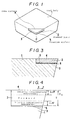
- FIG.1 shows a simple example of a polycrystalline diamond tool.
- a tool body (1) is made from cemented carbide.
- a polycrystalline diamond plate (2) is fixed on an end of the tool body (1) by a brazing layer (3).
- the diamond plate (2) has two surfaces.
- the outer surface revealed outside is called a rake surface (4).
- the inner surface concealed by the tool body (1) is here called a fixation surface.
- the impurity concentration is not uniform, but is changing along the direction vertical to the surface, namely along the direction of thickness.
- the impurity concentration near the fixation surface is higher than that near the rake surface in this invention.
- the diamond near the rake surface shall be grown by suppressing the inclusion of impurity as much as possible.
- the diamond near the fixation surface shall be grown with a material gas including the impurity added intentionally.
- the diamond on or near the rake surface shall be synthesized as a diamond of better quality with lower impurity concentration.
- the diamond on or near the fixation surface shall be synthesized as a diamond of worse quality with higher impurity concentration.
- the diamond in the vicinity of the fixation surface has low rigidity and enough elasticity. This is important. Enough elasticity or low rigidity can alleviate the strong stress applied on the rake surface by an object to be cut. Namely, the diamond on the fixation surface plays a role of a stress alleviation layer or shock absorber layer.
- the rigidity is low near the fixation surface but the rake surface has high rigidity.
- the structure heightens the toughness of the diamond plate as a whole without lowering the rigidity of the rake surface. Because of the high rigidity of the rake surface, the diamond tool has high abrasion resistance. In other words, this invention enables the diamond tool to heighten the chip resistance without damaging the excellent abrasion resistance of diamond.
- the impurity concentration of the diamond will be now expressed by the three dimensional coordinate.
- the z-axis is defined as the direction vertical to the surface of the diamond.
- the x-axis and the y-axis are defined as two vertical directions both of which are parallel to the surface of the diamond.
- the impurity concentration at the point ( x, y, z ) is represented by W ( x, y, z ).
- the original point of the coordinate exists on the rake surface.
- the thickness of the diamond plate is denoted by T.
- the first definition of the invention is expressed by the inequalities. T > 40 ⁇ m X 0 ⁇ Y 0
- a thickness of the diamond plate is more than 40 ⁇ m.
- the diamond thinner than 40 ⁇ m has not enough strength and is likely to be broken.
- maximum difference of height between the most worn-out spot and the least worn-out spot on the rake surface at the end of life time is more than 40 ⁇ m in most cases.
- the thickness shall preferably be 0.07 mm to 3.0 mm. Furthermore, if the production cost caused no serious problems, the diamond plate with the thickness more than 3 mm would be more profitable. Since diamond has the highest heat conductivity, the thicker the diamond plate is, the higher the heat diffusivity rises. The high heat diffusivity prevents the tool edge from being heated too hot.
- the most conspicuous feature of this invention is the inequality X0 ⁇ Y0 or X1 ⁇ Y1.
- the fixation surface would not act as a stress alleviation layer or a shock absorber layer and the diamond plate would be likely to be chipped and to be easily worn out.
- Both the rake surface and the fixation surface are suitable for measurement of impurity concentration, because they are exposed out.
- the impurity state or impurity concentration of diamond layers can be measured by the following methods ;
- the methods 1 and 2 enable us to observe the microscopic structure of diamond in addition to measuring the impurity concentration.
- the information of the microscopic structure around the impurities in diamond is obtainable.
- the methods 3to 9 make quantitative measurement of impurity concentration possible. These methods can measure only the impurity concentration on the surfaces as such. However, simultaneous sputtering of the diamond plate or microscope observation of the section of the diamond plate will bring about the information of impurity concentration at any depth.
- X1 is the average impurity concentration of a partial region with a depth of 30 % of the total thickness T from the rake surface.
- the impurity concentration Y1 of a fixation surface region can also be defined by
- Y1 is the average impurity concentration of another partial region with a depth of 30 % of the total thickness T from the fixation surface
- This invention can also be defined by the inequalities, X 1 ⁇ Y 1 T > 40 ⁇ m
- the impurity concentration X1 of the partial rake region with a depth of 30 % of the total thickness from the rake surface should be less than 5 percent.
- the impurity concentrarion X1 at the rake surface should preferably be very little for the sake of abrasion resistance. Less than 1% is more preferable. Most desirable impurity concentration is less than 1000 ppm ( 0.1% ).
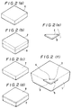
- the method for fabricating a diamond plate will be now briefly explained by means of FIG.2. Since the diamond plate is grown by the chemical vapor deposition methods, an easiest way to change the impurity concentration of diamond along the direction of thickness is changing the density of impurity in material gas continuously or stepwise ( either increasing monotonously or decreasing monotonously ). Increasing the density of impurity is more preferable than decreasing the density of impurity. The reason will be explained afterward.
- Material gas is supplied onto a substrate (6) heated in a CVD apparatus which will be explained in detail later. Being excited by some means, the material gas is dissolved into active radicals or ions and is reacted each other on the substrate. Diamond layer is growing on the substrate, which is shown by FIG.2(b). The density of impurity in the material gas is changing continuously or stepwise in this invention. After the diamond layer (7) has grown to the predetermined thickness on the substrate (6) by the CVD method, the substrate (6) is etched away by hydrofluoric, nitric acid ( mixture of hydrofluoric acid and nitric acid ) or aqua regia. Then a diamond plate is obtained ( FIG.2 (c) ).
- Diamond itself has poor wettability with the tool body made from cemented carbide. Then to improve the wettability between the tool body and the diamond plate, one surface of the diamond plate is metalized by evaporation coating (8) of metal ( FIG.2 (d) ). Then the diamond plate is divided into several chips of diamond with determined size suitable for the tool edge by a YAG laser ( FIG.2 (e) ). Then the metalized surface is fixed onto the edge surface of the tool ( FIG.2 (e) ). In those processes, it is also possible to divide the diamond plate earlier than to etch away the substrate.
- FIG.3 shows the sectional view of the tool fitted with the diamond plate.
- the tool body can be made from any hard metal. But preferably cemented carbide shall be employed as a material of the tool body.
- the tool edge has the edge surface on which the diamond plate is fixed through the intermediary of the metalized layer. Brazing is desirable to fix the diamond plate on the edge surface for the sake of high heat resistance and high strength.
- the diamond plate has two parallel surfaces.
- the free surface distanced far from the edge surface of the tool is the rake surface.
- a three dimensional coordinate is defined on the diamond plate.
- the x-axis and y-axis lie on the rake surface.
- the z-axis is defined along the direction of thickness from the rake surface to the fixation surface.
- the region held by the rake surface and the first dotted plane is the observation region on the side of the rake surface.
- the region held by the fixation surface and the second dotted plane is the observation region on the side of the fixation surface.
- the impurity concentration X1 and Y1 in these partial observation regions are put into question in this invention.
- the bottom surface in contact with the substrate is very smooth. But the free surface which has been formed near the end of the crystal growth becomes a rugged surface which is inherent in the CVD-grown polycrystal diamond. This is called hexa-octahedron structure of diamond. If the rugged free surface were assigned to be a rake surface, the rugged pattern of the rake surface would be transcribed on the surface of an object to be cut. To avoid the inconvenience, the rugged free surface which has grown at the end of the growth must be metalized and be fitted to an edge surface of a tool. Thus the smooth bottom surface which has been in contact with the substrate becomes the rake surface of the tool.
- the fixation surface must include more impurities than the rake surface, the density of impurity in the material gas shall be low at the beginning of the growth, shall monotonously be increased and shall be high at the end of the growth.
- Higher impurity concentration near the fixation surface is desirable also for the sake of structural point of view.
- High impurity concentration near the fixation surface decreases the thermal conductivity there .
- the lower thermal conductivity near the fixation surface will prevent the diamond plate from being taken off out of the tool end by hindering the heat from conducting to the brazing layer and melting it.
- the material gas includes in general ;
- any material including carbon which can be vaporized may be used as gas 2.
- alcohol and acetone are liquid at room temperature, they are vaporized by heating. Otherwise, they can be vaporized by bubbling them with hydrogen gas.
- hydrogen gas is not indispensable.
- hydrogen gas can be replaced by water ( H2O ), hydrogen peroxide ( H2O2 ), CF4, C2F6, C3F8, C-C4F8, C5F12, CHF3, CBrF3, CCl4, CCl3F, CCl2F2, CClF3, SF6, NF3, BCl3, F2, Cl2 or Br2 gas. Mixture of these gases are also available for material gas instead of H2.
- rare gases helium, neon, argon, krypton, xenon and radon
- the rare gas increases the density of active elements, e.g. hydrogen radicals or C2, prolongs the life time of the radicals and contributes to grow diamond with uniform quality.
- the substrate on which diamond shall be deposited is either W, Mo, Ta, Nb, Si, SiC, WC, W2C, Mo2C, TaC, Si3N4, AIN, Ti, TiC, TiN, B, BN, B4C, diamond, Al2O3 or SiO2.
- Cu or Al can be used as a substrate under the special conditions.
- the substrate is not necessarily a flat plate.
- This invention can also be applied to the tools having edges with adequate curvature, e.g. a twisted blade or an end mill blade. In this case, the substrate shall be the plate with the curvature as same as that of the tool blade.
- impurities mean in principle all materials except crystalline diamond.
- Appropriate impurities can be roughly sorted into two groups.
- First group of impurities contains carbon ingredients except crystalline diamond, e.g. crystalline graphite, amorphous carbon, etc.
- Second group contains metals, non-metals or their compounds.
- adequate impurities of the second group are silicon ( Si ), boron ( B ), aluminum ( Al ), tungsten ( W ), molybdenum ( Mo ), cobalt ( Co ), iron ( Fe ), niobium ( Nb ), tantalum ( Ta ).
- the carbides, oxides and nitrides of them are also available for impurities.
- the impurities are diffused in a crystalline diamond in the form of a single atom or a single molecule or diffused there in the form of powder with a diameter of 0.5 ⁇ m to 2 ⁇ m.
- the diamond including the first group of impurities can be made without adding impurities by intention. However, it can also be made by adding powder of graphite by intention.
- the diamond including the second group of impurities must be produced by doping impurities by intention.
- the impurities shall be doped in the form of halogenides of the impurities.
- halogenides for example, such fluorides, chlorides or bromides, WF6, WCl3, MoF6, MoCl3, SiF4, Si2F6, BCl3, ReF4, AlF3, FeCl3, SiCl4 are suitable impurities.
- These impurities are doped into diamond plates as a metal of W,Mo,Si,B or carbides of them, or halogen compounds as they are in the case of insufficient reaction. In any cases, high stability against heat or chemicals is obtainable.
- exceptionally silane gas ( SiH4 ) or diborane gas ( B2H6 ) can be used for impurities to be doped to the partial fixation region of diamond plates.
- powdered ceramics are also available for impurities for the diamond.
- Powder impurity can be doped into a diamond by dropping the powder intermittently to the growing diamond or by spraying the powder impurity on the material gas flow.
- the density of impurity shall be continuously or stepwise increased during the crystal growth in the CVD methods.
- Easier way is changing the ratio of impurity in two steps or three steps from lower ( or zero ) ratio to higher ratio.
- the easiest way is a two step growth comprising a first step in which no impurity is added and a second step in which a certain ratio of impurity is added to the material gas.
- diamond is grown by a material gas including a little quantity of halogenide gas, e.g. tungsten fluoride ( WF6 ) or boron chloride ( BCl3 ) in addition to hydrogen gas and methane gas. It is more desirable to increase the portion of methane / hydrogen in the latter step.
- the optimum ratio of impurity gas is a little affected by other conditions of growth. For example, if oxygen gas is mixed to the material gas, the ratio of impurity gas or hydrocarbon gas to hydrogen gas can be raised, because a small quantity of oxygen improves the quality of diamond.
- This invention grows the diamond plate with the impurity concentration changing along the direction of thickness by changing the composition of material gas supplied into the CVD apparatus.
- the diamond tool of this invention excels in strength, abrasion resistance, chip resistance, adhesion resistance and heat resistance.
- the reason why the diamond tool based on this invention is endowed with such properties is now explained.
- the diamond plates which have been synthesized by the CVD methods so far have uniform property overall without impurity.
- the diamond of high crystalline quality has very high rigidity. But the diamond is easily broken by an external shock. Namely, a good diamond of high crystalline quality lacks chipping resistance. Thus the tools having a good diamond plate are likely to be broken in a short time when they are used to cut or shave something. Perfect lattice structure of the diamond without impurity heightens the rigidity. Because of the high rigidity, the perfect diamond is likely to be chipped. High chipping resistance does not consist with high rigidity.
- the diamond with high impurity concentration excels in toughness or chipping resistance, because of the proper elasticity. But they are inferior to the diamond without impurity in strength, abrasion resistance, because of the low rigidity.
- a good tool requires both chipping resistance and abrasion resistance. Determining the impurity concentration within some range in the diamond plate does not give us a diamond tool with the most suitable properties.
- the surface which will contact with the objects to be cut requires high abrasion resistance.
- the toughness should be heightened to increase the chipping resistance. Toughness and rigidity are reciprocal properties. It is very difficult to heighten both the toughness and the rigidity of the same object.
- this invention gives complementary properties to the diamond plate along the direction of thickness.
- the rake surface which will come in contact with the objects is made from better diamond with lower impurity concentration.
- the rake surface has high abrasion resistance.
- the fixation surface which is fixed on the tool is made from worse diamond with higher impurity concentration.
- the fixation surface is rich in elasticity and toughness.
- the more elastic diamond near the fixation surface will alleviate and absorb the shock by shrinking.
- the elasticity of the diamond near the fixation surface endows the diamond tool with high quality.
- the abrasion resistance of a tool depends on the rake surface.
- the diamond on the rake surface has a highly ordered crystalline structure with high rigidity.
- the diamond tool reveals enough abrasion resistance even against the object difficult to cut or shave.
- the region held between the rake surface and the plane distanced from the rake surface by 30 % of thickness is made from the diamond of high quality.
- the high quality means low impurity concentration.
- the impurity concentration must be less than 5 at%.
- the optimum impurity concentration is less than 1000 ppm ( 0.1% ).
- the abrasion resistance is restricted by the binder. And adhesion resistance is also suppressed by the binder.
- the CVD grown diamond is inherently rich in abrasion resistance and adhesion resistance, because it includes no binder.
- the diamond tool of this invention is suitable for the tools which require high abrasion resistance, high chip resistance, high strength and high adhesion resistance, e.g. the tools for cutting, tools for grinding tools for digging or dressers.
- FIG.1 is a simplified perspective view of a polycrystalline diamond tool.
- FIG.2 is perspective views showing the steps for producing the polycrystalline diamond tool.
- FIG.3 is a sectional view of an edge of the diamond tool.
- FIG.4 is a sectional view of the diamond plate for showing the points for the impurity concentration measurement.
- FIG.5 is a schematic sectional view of a filament CVD apparatus.
- FIG.6 is a schematic sectional view of a microwave plasma CVD apparatus.
- FIG.7 is a schematic sectional view of a heat -exciting CVD apparatus.
- FIG.8 is a schematic sectional view of a heat plasma CVD apparatus.
- This invention can be applied to all the CVD methods which are able to synthesize diamond.
- the inventors have applied
- the substrate is a polycrystal silicon plate of 14 mm ⁇ 14 mm ⁇ 2.5 mm.
- One surface has been lapped with an abrasive containing granules of 0.5 ⁇ m to 5 ⁇ m in diameter until the maximum roughness R MAX became less than 0.8 ⁇ m ( R MAX ⁇ 0.8 ⁇ m ) and the flatness became less than 1 ⁇ m.
- the apparatuses for the CVD methods are explained. Then the results this invention has brought about on the apparatus will be described.
- FIG.5 shows a filament CVD apparatus.
- a susceptor (12) is installed in a vacuum chamber (11) .
- a substrate (13) is mounted on the susceptor (12).
- the vacuum chamber (11) has an exhaust outlet (14) which is connected to a vacuum pump (not shown in the figures ).
- Electrodes (15) are stood in the vacuum chamber (11).
- the electrodes (15) penetrate insulators (16) and are connected to a filament power source (21). Filaments (17) span the electrodes (15).
- Material gas is supplied into the vacuum chamber (11) through a gas inlet (18).
- a vacuum gauge (19) measures the degree of vacuum in the vacuum chamber (11). Cooling water (20) is introduced into the inner space of the susceptor (12) for cooling it.
- Three kinds of filaments made from different materials had been prepared.
- the diameter of all the filaments was 0.2 mm.
- Plural filaments were mounted in parallel with a distance of 4 mm.
- the distance between the filaments (17) and the substrate (13) was 5 mm.
- the temperature of the filaments (17) was measured by an optical thermometer.
- Samples A to D are embodiments of this invention and samples E to H are comparison examples based on the conventional method in Table 1.
- the components of material gas or the ratio of the components were changed with time.
- the substrate was coated in the material gas flow comprising 600 sccm of hydrogen gas (H2) and 5 sccm of methane gas (CH4) under 10666 Pa (80 Torr) by heating with the tungsten filament at 2150°C for 50 hours at the first step.
- the substrate was coated in the material gas flow comprising 600 sccm of hydrogen gas (H2) and 12.0 sccm of methane gas (CH4) and 2.0 sccm of tungsten fluoride gas (WF6) under 10666 Pa (80 Torr) by heating with the tungsten filament at 1800°C for 20 hours at the second step.
- sccm is a simplified expression of a unit of gas flow "standard cubic centimeter".
- 1 sccm means that 1 cm3 of gas reduced in the standard state i.e. at 0°C under 101325 Pa (1 atmosphere) flows per minute.
- the embodiment A changed the component and the component ratio of the material gas in two steps.
- Other two embodiments B and D changed the component and component ratio of the material gas in two steps.
- the embodiment C changed the components or component ratio of the material gas in four steps.
- the comparison example F synthesized diamond with the material gas with low density of carbon in a single step also.
- the comparison example H changed the impurity ratio of the material gas in two steps in contradiction to this invention.
- the first layer is a layer nearer to the rake surface and the second layer is a layer nearer to the fixation surface in the samples A, B, D and H.
- the measurements of the impurity concentration were done by the SIMS (Secondary Ion Mass Spectroscopy) or IMA (Ion Microanalyzer). where undetectable means that the impurity concentration is less than 3 ppm in the carbon matrix.
- the samples A to D are embodiments of this invention.
- the sample E to G are comparison examples which have no partial layers, because the material gas had not been changed stepwise as shown in Table 1.
- the sample I is a natural diamond II a fixed on a tool as a comparison sample for the impurity concentration measurement.
- the sample J is another comparison sample. This is a sintered diamond which was made by sintering the diamond polycrystalline powder of 10 ⁇ m in average diameter including cobalt (Co) of 10 volume % under high pressure.
- the sample J was not made by the CVD methods. Since the sample J is a cutting chip with a sintered diamond fitted to the tool, it includes high density of Co (10 %) nearly uniformly.
- the observation points are defined by the distance z ( ⁇ m) from the rake surface as shown in FIG.4.
- the layers 1 and 2 are the partial layers caused by changing the components or component ratio in the material gas. Since the side which had deposited at the beginning of the growth was assigned to be a rake surface, the steps 1 and 2 in Table 1 correspond to the layers 1 and 2 respectively. As a matter of course, impurity concentration is smaller near the rake surface in the embodiments.
- the comparison example H changed the impurity concentration of diamond in the material gas stepwise in contradiction to the teaching of this invention in the CVD growth.
- the grown diamond has also the contradictory distribution to this invention regarding the impurity concentration.
- All the embodiments A to D increased the ratio of impurity in the material gas.
- the impurity concentration increases along the direction of growth i.e. the direction from the rake surface to the fixation surface.
- the object to be cut is a round bar with four axial grooves made from A 390 alloy (Al - 17 % Si). speed for cutting : 800 m/min depth of cutting: 0.2 mm feed : 0.1 mm/rev.
- Another comparison example J i.e. sintered diamond, was not broken down. But the average abrasion loss in 90 minute cutting was 95 ⁇ m, which is far larger than that of the embodiments. Since the sintered sample J contains the binder, e.g. cobalt (Co), the binder would lower the abrasion resistance.
- the binder e.g. cobalt (Co)
- the diamond plate of this invention has lower impurity concentration near the rake surface and high impurity concentration near the fixation surface.
- Non-uniformity of impurity concentration is the essential feature of this invention.
- the diamond near the fixation surface with adequate elasticity alleviates the strong force acting on the rake surface and heightens the chipping resistance overall.
- Samples A to D embodiments of this invention have high abrasion resistance. Namely, 90 minutes abrasion loss is little. They are immune from breakdown by chipping.
- the samples A to D have the distribution of impurity concentration defined by the inequality X1 ⁇ Y1 or X0 ⁇ Y0 which has been formed by changing the ratio of impurity in material gas in the growth of the vapor phase deposition methods.
- X0 is an impurity concentration on the rake surface of a diamond plate.
- Y0 is an impurity concentration on the fixation surface of the diamond plate.
- X1 is an average impurity concentration of the rake partial region within a depth of 30 % of the total thickness from the rake surface.
- Y1 is an average impurity concentration of the fixation partial region within a depth of 30 % of the total thickness from the fixation surface.
- X1 or Y1 can otherwise be defined as an average impurity concentration of the partial regions within a depth of 20 % or 40 % of the total thickness.
- Halogen elements or Halogenide compounds are suitable for impurities to be doped into the region near the fixation surface. Introduction of these gases are facile enough. Excess impurity concentration is forbidden. The impurity concentration must be less than 5 % at the rake surface. More than 5 % of impurity concentration at the rake surface would deteriorate abrasion resistance devastatingly. On the contrary the impurity concentration near the rake surface is preferably less than 1000ppm. Lower impurity concentration will heighten the abrasion resistance at the rake surface.
- the thickness of the diamond plate must be more than 40 ⁇ m.
- a diamond plate thinner than 40 ⁇ m would be likely to be broken owing to the lack of strength.
- Another reason is that the difference of height between the most worn out spots and the least worn out spots is often more than 40 ⁇ m at the end of the life time of the tools.
- Such a diamond plate with a thickness of 0.07 mm to 3.0 mm is preferable.
- a thick blade suppresses the rising of the temperature of blade by heightening the heat diffusivity. Thus the abrasion resistance is raised.
- FIG.6 shows the apparatus.
- a quartz bar (23) supports a substrate (24) on its top end.
- material gas (26) is introduced into the quartz cylinder (22).
- Exhaust gas is exhaled from a gas outlet (27) below.
- a cooling water jacket (28) is equipped around the reaction region of the quartz cylinder (22).
- a magnetron (29) generates microwave (33).
- the microwave (33) propagates through a waveguide (30) to the vicinity of the substrate (24).
- the microwave excites the material gas to plasma or neutral radicals.
- High density of plasma (31) is generated around the substrate (24).
- the waveguide is at right angles to the quartz cylinder (22) and the microwave propagates at right angles to the quartz cylinder.
- another geometric relations between the waveguide and the quartz cylinder can be chosen as long as high density plasma is induced by the microwave oscillation.
- the shape and the size of the waveguide determine the mode of microwave.
- a plunger (32) carrying a reflector can be displaced in the waveguide (30). Since the frequency of the microwave is predetermined ( e.g.2.45 GHz ), the mode of the standing wave is uniquely determined by the position of the plunger.
- the microwave CVD apparatus belongs to state of arts.
- the material gas comprises carbon containing gas, hydrogen gas and impurity gas.
- magnets are furnished around the quartz cylinder for generating the cusp magnetic field or the axial magnetic field for confining the plasma within a small space near the substrate.
- Table 4 shows the conditions for synthesizing diamond by the microwave plasma CVD method.
- the substrates were polycrystalline silicon plates of 14 mm ⁇ 14 mm ⁇ 2.5 mm.
- the silicon plates has been lapped by abrasive granules with diameters of 0.5 ⁇ m to 5 ⁇ m till the roughness became less than 0.8 ⁇ m (R max ⁇ 0.8 ⁇ m) and the flatness became less than 1 ⁇ m (flatness ⁇ 1 ⁇ m).
- the temperature of the substrate was monitored by the optical thermometer during the deposition.
- the temperature data were calibrated by the data obtained by measuring them by a thermocrayon.
- the substrates were heated to a temperature between 400°C and 950°C.
- Samples K to N are embodiments of this invention. These embodiments changed the components or the component ratio of material gas in two steps or four steps to increase the impurity concentration in later steps.
- WF6, BCl3, F2 or FeCl3 were doped as an impurity like embodiments 1.
- Rare gas, e.g Ar was added to excite the microwave plasma stably and to increase the density of active radicals, e.g. H ⁇ and C2.
- Samples O to Q are comparison examples.
- the samples O and P were synthesized overall by the material gas without impurity.
- the sample Q changed the component ratio of impurity in the material gas in contradiction to this invention.
- the diamond plates were cut into four triangles. Cutting chips were made by fitting the diamond plates on tools. The measurements of the impurity concentration were done on the tools. Table 5 shows the results of the measurements.
- the diamond tools were estimated by the cutting performance test.
- the test object to be cut was a round bar of alloy A390 ( Al-17%Si ) with four axial grooves on the outer surface.
- the conditions of dry cutting were ; speed for cutting : 800 m/min depth for cutting: 0.2 mm feed : 0.1 mm/rev.
- Table 6 shows the results of the cutting performance test.
- Table 6 CUTTING PERFORMANCE OF THE DIAMOND SYNTHESIZED BY MICROWAVE PLASMA CVD METHOD SAMPLE V b ABRASION LOSS ( ⁇ m) EMBODIMENTS K average abrasion loss in 90 minute cutting 19 ⁇ m L average abrasion loss in 90 minute cutting 16 ⁇ m M average abrasion loss in 90 minute cutting 22 ⁇ m N average abrasion loss in 90 minute cutting 17 ⁇ m COMPARISON EXAMPLES O 30 second cutting, breakdown by chipping P average abrasion loss in 50 second cutting 150 ⁇ m Q 1 minute cutting, breakdown by chipping
- the average abrasion loss in 90 minute cutting of the diamond tools of this invention was very little (10 ⁇ m to 20 ⁇ m). Therefore, the diamond tools are suitable for practical use.
- the comparison examples O and P in which no impurity (except carbon ingredients) was detected, were broken down or worn out seriously in a short time.
- the specific gravity of the sample P is 2.7 g/cm3 at the partial region from the rake surface to a depth of 10 ⁇ m ,and is 2.7g/cm3 too at the partial region from a depth of 90 ⁇ m to a depth of 100 ⁇ m. Since it is less than the specific gravity of pure diamond, the sample P must include some carbon ingredients except diamond.
- the sample P includes tantamount carbon ingredients uniformly both in the rake surface region and in the fixation surface region. Therefore it must lack abrasion resistance entirely,although the carbon ingredients raises the chipping resistance. From the measurement of specific gravity , the sample P is assumed to contain nearly 36wt% of carbon ingredients except diamond.
- the comparison example Q with the impurity distribution in contradiction to this invention was broken down owing to the lack of toughness.
- Another polycrystalline diamond plates were fabricated by the heat-exciting CVD method.
- FIG.7 shows the heat-exciting CVD apparatus.
- a quartz chamber (35) is a chamber which can be made vacuous.
- a susceptor (36) stands in the quartz chamber (35).
- a substrate (37) is mounted on the susceptor (36).
- a heater (38) is furnished around the quartz chamber (35).
- Material gas is Inhaled through a gas inlet (39) into the quartz chamber (35).
- Exhaust gas is exhaled through a gas outlet (40). Since the material gas is excited by heat, polycrystalline diamond is deposited on the substrate, being synthesized by the vapor phase chemical reaction.
- the substrate is a polycrystalline silicon plate of 14 mm ⁇ 14 mm ⁇ 2.5 mm.
- the ratio of impurity gas in the material gas was changed in two steps.
- the conditions for synthesis for each step were ; ( First step ) conditions .... heat-exciting CVD method ( Second step ) conditions ( following 1st step ) ... heat-exciting CVD method material gas H2 : 1000 sccm CH3Br : 18 sccm F2 : 18 sccm He : 150 sccm WF6 : 2.5 sccm pressure : 13332 Pa (100 Torr) substrate temperature : 100 °C thickness : 100 ⁇ m
- the impurity concentration measurement was carried out to the diamond plate.
- the impurity concentration for the first and the second layers were, first layer ... ( at the point distanced by 10 ⁇ m from the rake surface ) F 0.02% second layer ... ( at the point distanced by 165 ⁇ m from the rake surface ) W 1.6% Br 0.1% F 0.12%
- the impurity concentration was higher in the second layer made by the material gas with higher density of impurities.
- V b abrasion loss in 120 minute cutting was 15 ⁇ m. This result shows that this invention is also applicable to the heat-exciting CVD method.
- FIG.8 shows the heat plasma CVD apparatus.
- coaxial electrodes (43) are equipped on an upper wall of a vacuum chamber (42).
- a susceptor (44) is installed below the electrodes (43).
- a substrate (45) is mounted on the susceptor (44).
- the inner electrode is a cathode and the outer electrode is an anode. Some voltage is applied between the anode and the cathode by the direct current power source (46).
- material gas (47) Passing through the gap between the anode and the cathode, material gas (47) is inhaled into the vacuum chamber (42) via a nozzle (51). Being ionized to plasma gas by the action of discharge between the electrodes (43), the ionized material gas (47) flows toward the substrate (45). The ionized material gas reacts in vapor phase. The synthetic is deposited on the substrate. Exhaust gas is exhaled from the gas outlet (49) to a vacuum pump (not shown in the figures ).
- the substrate is a silicon polycrystal plate of 14 mm ⁇ 14 mm ⁇ 2.5 mm like the embodiment 3.
- first step conditions for growth ... heat plasma CVD
- second step conditions for growth .... heat plasma CVD
- material gas H2 10 slm CH4 : 2.8 slm H e : 20 slm F2 : 0.1 slm WF6 : 0.2 slm pressure : 26664 Pa (200 Torr)
- substrate temperature 500 °C thickness of growth: 300 ⁇ m where "slm" (standard litter per minute) is a unit of gas flow.
- 1 slm means 1 litter of gas reduced to the standard state i.e. at 0°C under 101325 Pa (1 atm) flows per minute.
- Total thickness of the diamond was 500 ⁇ m (0.5 nm).
- a diamond tool was made by brazing the diamond plate onto a tool body. The impurity concentration measurement was done to the first layer and the second layer.
- the impurity concentration of the layers were ; (1)first layer (at 40 ⁇ m depth from the rake surface) F 0.12% (2)second layer (at 455 ⁇ m depth from the rake surface) W 3.8% Br 1.2% F 0.22%
- V b abrasion loss in 120 minute cutting was 30 ⁇ m. This was a very small loss. This result shows that this invention is also applicable to the heat plasma CVD method.
- a substrate was mounted on the susceptor (44) in Fig.8.
- Diamond was grown on the substrate (45) by the heat plasma CVD method comprising two steps of deposition.
- the material gas included no impurity.
- the powder of silicon carbide (SiC) with diameters of 2 ⁇ m to 5 ⁇ m was introduced into the chamber on the second step as an impurity.
- first step condition of growth
- heat plasma CVD material gas H2 10 slm C2H2 : 0.5 slm pressure : 6666 Pa (50 Torr)
- substrate temperature : 850 °C thickness of growth: 300 ⁇ m
- second step condition of growth ... heat plasma CVD (following 1st step)
- the polycrystalline diamond plate was brazed on a tool body according to the processes shown in Fig.2.
- the impurity concentration of the layers was measured.
- first layer at a point distanced by 60 ⁇ m from the rake surface
- second layer at a point distanced by 900 ⁇ m from the rake surface
- a substrate was mounted on the susceptor (12) in Fig.5.
- Diamond was grown on the substrate by the filament CVD method comprising two steps of deposition for changing the impurity ratio in the material gas. No impurity was included in the material gas of the first step.
- the second step used a material gas with high ratio of hydrocarbon gas in order to grow such diamond having much non-crystalline diamond carbon ingredient.
- (first step) condition of growth ...
- filament CVD material gas H2 1000 sccm CH4 : 8 sccm pressure : 15999 Pa (120 Torr)
- W filament temperature 2150 °C substrate temperature : 800 °C thickness of growth: 150 ⁇ m
- second step condition of growth ...
- a tool was fabricated by brazing the diamond plate to an end of a tool body according to the processes of Fig.2.
- the impurity concentration of each layer was calculated from the results of measurement of specific gravity of the diamond plate, assuming that the specific gravity of crystalline diamond is 3.52 g/cm3.
- first layer at a point distanced by 30 ⁇ m from the rake surface
- second layer at a point distanced by 750 ⁇ m from the rake surface
- non-diamond carbon ingredient 2 % ⁇ 6 % metal impurity .... W 0.1% (IMA)
- the tool with less than 5 % of impurity concentration can cut the difficult test object ( 25 % Si-Al ). More preferable impurity concentration is less than 1 %. Less than 1000 ppm is the most preferable impurity concentration at the rake surface.
Landscapes
- Chemical & Material Sciences (AREA)
- Engineering & Computer Science (AREA)
- General Chemical & Material Sciences (AREA)
- Chemical Kinetics & Catalysis (AREA)
- Materials Engineering (AREA)
- Mechanical Engineering (AREA)
- Metallurgy (AREA)
- Organic Chemistry (AREA)
- Inorganic Chemistry (AREA)
- Plasma & Fusion (AREA)
- Physics & Mathematics (AREA)
- Combustion & Propulsion (AREA)
- Crystallography & Structural Chemistry (AREA)
- Crystals, And After-Treatments Of Crystals (AREA)
- Chemical Vapour Deposition (AREA)
- Cutting Tools, Boring Holders, And Turrets (AREA)
- Carbon And Carbon Compounds (AREA)
Description
- This invention relates to a polycrystalline diamond tool which excels in strength, abrasion resistance, chip resistance, adhesion resistance and heat resistance and is suitable for cutting tools or abrasion resistance tools.
- All polycrystalline diamonds for tools have hitherto been produced by the sintering method. Namely, diamond powder - polycrystalline diamond granules - is charged in a mold, is put under high pressure, is heated to a high temperature and is kept for a certain time at the high temperature under high pressure. Diamond granules are coupled together by the action of the heat and the pressure. Thus powder is integrated into a body. The shape of the sintered body is determined by the mold. Sintered diamond has been used on cutting devices for nonferrous metals, drill bits and drawing dies.
- For example, the Japanese Patent Publication No.52-12126 disclosed a sintered body of diamond including cobalt by about 10 to 15 volume percent which was made by sintering diamond powder being kept in contact with the cemented carbide of group WC-Co ( tungsten carbide- cobalt ),diffusing some part of cobalt into the diamond powder as a binder metal. The sintered diamond body including cobalt as solid solution is gifted with a practical utility for cutting tools for nonferrous metals. In general, since diamond has the tendency to be alloyed with iron or steel, diamond tool is not used on cutting ferrous metals.
- However, the sintered diamond has a drawback of the poor heat resistance. The abrasion resistance and the strength of the sintered body of diamond are greatly lowered by being heated above 700°C. The sintered body of diamond is destroyed by being heated above 900°C.
- Single crystal diamond or polycrystalline diamond has high heat resistance. Why is the heat resistance of the sintered diamond so poor ? One reason is that diamond is partly converted to graphite on the boundary between the diamond granules and the cobalt solid solution at high temperature. Conversion of diamond into graphite lowers the strength and the abrasive resistance, because graphite is weaker than diamond in strength. Another reason is that the difference of the thermal expansion between cobalt and diamond generates strong thermal tension at the boundary between the diamond granules and the cobalt solid solution.
- To improve the poor heat resistance of the sintered body of diamond, the Japanese Patent Laying Open No.53-114589 proposed a sintered body of diamond which is rid of cobalt as a binder metal by treating the sintered diamond body with acid. The sintered diamond body must be immune from the problems of the graphite conversion and the thermal tension which would occur at the boundary of the diamond granules and the cobalt solid solution, since the sintered body includes no cobalt. However, the sintered diamond body without cobalt becomes severely porous, because the spaces where cobalt has occupied are left as holes after cobalt is dissolved away by acid. Although the heat resistance is raised by washing cobalt away, the mechanical strength of the sintered body is lowered because of the porosity. The diamonds produced by the sintering method are accompanied by these drawbacks. The sintering method at present cannot satisfy the requirements of both mechanical strength and heat resistance.
- Recently, a new technology which enables us to synthesize diamond polycrystals chemically from vapor phase has been developed. This technology is called a chemical vapor phase deposition ( CVD ) method or simply a vapor phase synthesis. The method comprises the steps of diluting hydrocarbon gas with hydrogen gas to less than 5 volume percent, introducing the mixture gas into a reactor under the pressure of several tens Torr ( several thousands Pa ), exciting the material gas for resolving it to an active state by some means and depositing diamond on the substrate heated at a certain temperature. With regard to the means for exciting the material gas, various means have been proposed, e.g. heating by filament heater or exciting the material gas by electrons or plasma. Some different CVD methods have been proposed according to the means for excitation of material gas.
- The Japanese Patent Laying Open No.58-91100 ('83) proposed a method comprising the steps of preheating the material gas by a hot electron emission material heated above 1000°C, introducing the preheated material gas onto a heated substrate, resolving hydrocarbon to active states, e.g. ions, electrons and neutral radicals and depositing a diamond polycrystal on the substrate.
- The Japanese Patent Laying Open No.58-110494 ('83) proposed a method comprising the steps of exciting hydrogen gas into plasma by the microwave electrodeless discharge, mixing the plasma-excited hydrogen with hydrocarbon gas and depositing a diamond polycrystal on a heated substrate.
- Thus, there are various kinds of the CVD methods for growing diamond crystals according to the means for excitation
- Diamond polycrystals are grown by the CVD methods. There are two ways for applying the diamond polycrystals to tools. One is separating the diamond polycrystal from the substrate and fitting the diamond polycrystal to an end of a tool. The other is depositing the diamond polycrystal directly on an edge of a tool instead of a substrate. The edge of the tool is reinforced by the diamond coating.
- Japanese Patent Laying Open No.1-153228 ('89) and the Japanese Patent Laying Open No.1-210201 ('89) proposed a method for producing a diamond tool comprising the steps of depositing a diamond polycrystal on a substrate by a chemical vapor deposition ( CVD ) method, etching the substrate away with acid or other pertinent solution and fitting the separated diamond polycrystal to an edge of a tool which is made of metal. However, the diamond tool consisting of a diamond edge and a metal body lacks chip resistance and abrasion resistance. The " chip resistance " is here defined as the strength for keeping its shape against an external shock without being cracked away. Low chip resistance means being likely to be cracked by an external shock. The " abrasion resistance " is here defined as the strength against abrasion. Low abrasion resistance means being likely to be abraded easily. Intrinsically diamond should have high abrasion resistance and high chip resistance, but the diamond crystal synthesized by the present CVD methods is not endowed with the high abrasion resistance and high chip resistance by some unknown reasons.
- The tools whose edge is coated with polycrystalline diamond have also been proposed. On whole of a tool or on a part of a tool as a substrate, diamond polycrystal is grown by the CVD method. Since the edge of the tool is coated with diamond, the edge would have enough strength. However, the CVD coated tools in practice show poor performance - weak strength, low chip resistance and low abrasion resistance. The reason of the poor performance is partly because the diamond polycrystal is too thin, partly because the adhesion force between the diamond and the tool metal is insufficient and partly because the diamond is likely to peel off from the metal surface. However, it is difficult to heighten the adhesion strength, since the tool metal and the diamond are totally different with regard to many physical or chemical properties, e.g. crystal structure, conductivity, thermal expansion.
- The Japanese Patent Laying Open No.2-22471 ('90) proposed an improved CVD coated tool. The adhesion strength is heightened by coating a cemented carbide tool with an improved diamond compound. However, such a diamond coated tool often shows poor cutting performance dependent on the roughness of the object to be cut. Further, the cutting performance of the tool is totally Insufficient, when it cuts the hard objects with high cutting resistance, e.g. Al - 17% Si alloy ( Al 83%,
Si 17% ), Al - 25% Si alloy ( Al 75 %,Si 25 % ). - EP-A-0279898 describes a tool with a wear-protective coating. The coating comprises a plurality of layers formed by chemical vapour deposition. Each later contains a different proportion of diamond ranging from 10% by weight for the innermost layer to 100% by weight in the outermost layer. The other component is cobalt.
- An object of the invention is to provide a polycrystalline diamond tool with high strength, high adhesion resistance, high heat resistance, and high abrasion resistance.
- Another object of the invention is to provide a polycrystalline diamond tool which excels in chip resistance and abrasion resistance for cutting the hard objects with high cutting resistance.
- Another object of the invention is to provide a method for producing a polycrystalline diamond with high strength, high adhesion resistance, high heat resistance and high abrasion resistance.
- According one aspect of the present invention there is provided a polycrystalline diamond tool comprising a tool body having an edge surface, and a polycrystalline diamond plate carried on said edge surface, said plate having a rake surface and a fixation surface and being more than 40 µm in thickness, and the plate having an impurity concentration which changes under direction of its thickness, such that the impurity concentration at the rake surface is less than 5% and is lower than the impurity concentration at the fixation surface, characterised in that the plate has been produced as a separate element by a vapour phase deposition method onto a substrate, separated from that substrate, and secured to the edge surface of the body by a brazing layer in such a way that the surface which has been separated from the substrate becomes the rake surface.
- According to another aspect of the present invention there is provided a method for producing a polycrystalline diamond tool comprising the steps of; supplying material gas including at least a carbon-containing gas, and hydrogen gas and optionally as impurity gas into a vacuum chamber, exciting the material gas into the state including plasma or radicals, introducing the material gas to a heated substrate, depositing diamond on the substrate with the material gas without impurity or with little impurity in an earlier step such that the impurity concentration is less than 5%, increasing the ratio of impurity in the material gas, depositing diamond on the substrate with the material gas with much impurity in a later step till the diamond becomes more than 40 µm in thickness, etching the substrate away from the deposited diamond by an etchant, obtaining a diamond plate, metalizing the surface of the diamond plate which has grown in the later step, fixing the metalized surface on an end surface of a tool body and obtaining a diamond tool with a rake surface which has grown in the earlier step and with a fixation surface which has grown in the later step.
- According to a further aspect of the present invention there is provided a method for producing a polycrystalline diamond tool comprising the steps of; supplying material gas including at least a carbon-containing gas and hydrogen gas and optionally a powder of impurity into a vacuum chamber, exciting the material gas into the state including plasma or radicals, introducing the material gas to a heated substrate, depositing diamond on the substrate with the material gas without impurity or with little impurity in an earlier step, such that the impurity concentration is less than 5% increasing the ratio of impurity in the material gas, depositing diamond on the substrate with the material gas with much impurity in a later step till the diamond becomes more than 40 µm in thickness, etching the substrate away from the deposited diamond by an etchant, obtaining a diamond plate, metalizing the surface of the diamond plate which has grown in the later step, fixing the metalized surface on an end surface of a tool body and obtaining a diamond tool with a rake surface which has grown in the earlier step and with a fixation surface which has grown in the later step.
- The polycrystalline diamond tool of one embodiment of this invention comprises a tool body with an end having an end surface and a diamond polycrystal plate for fitting on the end surface of the tool body, the diamond polycrystal plate being more than 40µm in thickness, wherein the impurity concentration of the diamond plate changes in the direction vertical to the surfaces, (i.e. in the direction of thickness ), the impurity concentration ( X₀% ) at the rake surface is lower than the impurity concentration ( Y₀% ) at the fixation surface. Namely X₀ < Y₀ is the characteristic of this Invention. Lower impurity concentration of diamond at the rake surface gives the diamond plate high strength, high abrasion resistance and high adhesion resistance. On the contrary, higher impurity concentration at the fixation surface heightens the chip resistance by alleviating the stress applied on the rake surface, since higher impurity concentration heightens the toughness because of the low rigidity owing to the numerous impurities.
- Both the diamond near the rake surface and the diamond near the fixation surface cooperate to give the tool ideal characteristics by compensating the weak points of the counterparts with their strong points. Therefore, the essential feature of this invention depends on a complementary principle between the rake surface and the fixation surface.
- All the CVD deposited diamonds of the prior art have uniform impurity concentration. However, the diamond of this invention has varying impurity concentration in the direction of thickness ( vertical to the plane ) : higher impurity concentration at the fixation surface for being mounted on an edge of a tool and lower impurity concentration at the rake surface for cutting objects.
- An easy method for fabricating a diamond plate with the impurity concentration varying in the direction of thickness is varying the component of material gas during the deposition. At an earlier stage of deposition, pure hydrocarbon and hydrogen gases should be supplied. At a later stage, a gas including an impurity should be mixed into hydrocarbon and hydrogen gases.
- Although this invention has been defined by the impurity concentration only of both surfaces of diamond so far, this invention can also be defined by the impurity concentration of partial regions with a certain depth from the rake surface and the fixation surface.
- The average impurity concentration in a partial region within a depth of 30 % of total thickness from the rake surface is designated by X₁. The average impurity concentration in another partial region within a depth of 30 % of total thickness from the fixation surface is designated by Y₁. This invention can be also defined by another inequality X₁ < Y₁. If the impurity concentration is monotonously changing in the direction of thickness ( vertical to the surface ), the first definition X₀ < Y₀ and the second definition X₁ < Y₁ are entirely equivalent. Here " monotonously " means the mode of change which does not repeat both increasing and decreasing. " Monotonous " decrease means that the mode of change includes only decreasing and keeping constant. " Monotonous "Increase means that the mode of change includes only increasing and keeping constant. Practically, the impurity concentration shall be continuously or stepwise, increasing or decreasing in the vapor phase deposition of diamond. Repetition of decrease and increase of impurity concentration shall be forbidden.
- However, since the impurity concentration at the surfaces of the diamond plates manufactured by the CVD methods shall be accompanied by fluctuation, the first definition X₀ < Y₀ is not necessarily sufficient. The second definition X₁ < Y₁ satisfactorily defines this invention despite fluctuation of impurity concentration, because X₁ and Y₁ define the impurity concentration in the partial regions with a certain thickness. However, the first definition X₀ < Y₀ may be more convenient for measuring the impurity concentration.
- FIG.1 shows a simple example of a polycrystalline diamond tool. A tool body (1) is made from cemented carbide. A polycrystalline diamond plate (2) is fixed on an end of the tool body (1) by a brazing layer (3). The diamond plate (2) has two surfaces. The outer surface revealed outside is called a rake surface (4). The inner surface concealed by the tool body (1) is here called a fixation surface. In this invention, the impurity concentration is not uniform, but is changing along the direction vertical to the surface, namely along the direction of thickness. The impurity concentration near the fixation surface is higher than that near the rake surface in this invention.
- The diamond near the rake surface shall be grown by suppressing the inclusion of impurity as much as possible. On the contrary , the diamond near the fixation surface shall be grown with a material gas including the impurity added intentionally.
- The diamond on or near the rake surface shall be synthesized as a diamond of better quality with lower impurity concentration. The diamond on or near the fixation surface shall be synthesized as a diamond of worse quality with higher impurity concentration.
- Because of the higher impurity concentration, the diamond in the vicinity of the fixation surface has low rigidity and enough elasticity. This is important. Enough elasticity or low rigidity can alleviate the strong stress applied on the rake surface by an object to be cut. Namely, the diamond on the fixation surface plays a role of a stress alleviation layer or shock absorber layer.
- In the structure of the diamond plate, the rigidity is low near the fixation surface but the rake surface has high rigidity. The structure heightens the toughness of the diamond plate as a whole without lowering the rigidity of the rake surface. Because of the high rigidity of the rake surface, the diamond tool has high abrasion resistance. In other words, this invention enables the diamond tool to heighten the chip resistance without damaging the excellent abrasion resistance of diamond.
- For defining the invention more strictly, the impurity concentration of the diamond will be now expressed by the three dimensional coordinate. The z-axis is defined as the direction vertical to the surface of the diamond. The x-axis and the y-axis are defined as two vertical directions both of which are parallel to the surface of the diamond. The impurity concentration at the point ( x, y, z ) is represented by W ( x, y, z ). The original point of the coordinate exists on the rake surface. Then z = 0 means the rake surface. The thickness of the diamond plate is denoted by T. Thus z = T means the fixation surface.
- For defining the invention by the impurity concentration, impurity concentration X₀ and Y₀ on the rake surface and on the fixation surface are defined by


- The reason why a thickness of the diamond plate is more than 40 µm will be now explained. One reason is that the diamond thinner than 40 µm has not enough strength and is likely to be broken. Another reason is that maximum difference of height between the most worn-out spot and the least worn-out spot on the rake surface at the end of life time is more than 40 µm in most cases.
- If higher abrasion resistance is required, the thickness shall preferably be 0.07 mm to 3.0 mm. Furthermore, if the production cost caused no serious problems, the diamond plate with the thickness more than 3 mm would be more profitable. Since diamond has the highest heat conductivity, the thicker the diamond plate is, the higher the heat diffusivity rises. The high heat diffusivity prevents the tool edge from being heated too hot.
- The most conspicuous feature of this invention is the inequality X₀ < Y₀ or X₁ < Y₁. On the contrary, if X₀ ≧ Y₀ or X₁ ≧ Y₁, the fixation surface would not act as a stress alleviation layer or a shock absorber layer and the diamond plate would be likely to be chipped and to be easily worn out.
- Next question is how to measure the impurity concentration in a diamond plate.
- Both the rake surface and the fixation surface are suitable for measurement of impurity concentration, because they are exposed out. The impurity state or impurity concentration of diamond layers can be measured by the following methods ;
- ① TEM ( Transmission Electron Microscopy )
- ② TED ( Transmission Electron Diffraction )
- ③ SIMS ( Secondary Ion Mass Spectroscopy )
- ④ XPS ( X-ray Photoelectron Spectrometry )
- ⑤ IMA ( Ion Microanalyzer )
- ⑥ EDX ( Energy Dispersive X-ray Spectrometry )
- ⑦ WDX ( Wide Dispersive X-ray Spectrometry )
- ⑧ EPMX ( Electron Probe X-ray Microanalyzer )
- ⑨Measurement of Specific Gravity
- The
methods ① and ② enable us to observe the microscopic structure of diamond in addition to measuring the impurity concentration. The information of the microscopic structure around the impurities in diamond is obtainable. The methods ③to ⑨make quantitative measurement of impurity concentration possible. These methods can measure only the impurity concentration on the surfaces as such. However, simultaneous sputtering of the diamond plate or microscope observation of the section of the diamond plate will bring about the information of impurity concentration at any depth. - As mentioned before, this invention can be defined by the impurity concentration in partial regions with definite thickness in the direction vertical to the surface. Here, the impurity concentration X₁ of a rake region can be defined by


- Y₁ is the average impurity concentration of another partial region with a depth of 30 % of the total thickness T from the fixation surface
- This invention can also be defined by the inequalities,


- However, too much impurity concentration is undesirable for the partial region near the rake surface. Excess impurity concentration would lower the abrasion resistance by impairing the strength of the edge of tools. Therefore, the impurity concentration X₁ of the partial rake region with a depth of 30 % of the total thickness from the rake surface should be less than 5 percent.

- The method for fabricating a diamond plate will be now briefly explained by means of FIG.2. Since the diamond plate is grown by the chemical vapor deposition methods, an easiest way to change the impurity concentration of diamond along the direction of thickness is changing the density of impurity in material gas continuously or stepwise ( either increasing monotonously or decreasing monotonously ). Increasing the density of impurity is more preferable than decreasing the density of impurity. The reason will be explained afterward.
- Material gas is supplied onto a substrate (6) heated in a CVD apparatus which will be explained in detail later. Being excited by some means, the material gas is dissolved into active radicals or ions and is reacted each other on the substrate. Diamond layer is growing on the substrate, which is shown by FIG.2(b). The density of impurity in the material gas is changing continuously or stepwise in this invention. After the diamond layer (7) has grown to the predetermined thickness on the substrate (6) by the CVD method, the substrate (6) is etched away by hydrofluoric, nitric acid ( mixture of hydrofluoric acid and nitric acid ) or aqua regia. Then a diamond plate is obtained ( FIG.2 (c) ).
- Diamond itself has poor wettability with the tool body made from cemented carbide. Then to improve the wettability between the tool body and the diamond plate, one surface of the diamond plate is metalized by evaporation coating (8) of metal ( FIG.2 (d) ). Then the diamond plate is divided into several chips of diamond with determined size suitable for the tool edge by a YAG laser ( FIG.2 (e) ). Then the metalized surface is fixed onto the edge surface of the tool ( FIG.2 (e) ). In those processes, it is also possible to divide the diamond plate earlier than to etch away the substrate.
- FIG.3 shows the sectional view of the tool fitted with the diamond plate. The tool body can be made from any hard metal. But preferably cemented carbide shall be employed as a material of the tool body. The tool edge has the edge surface on which the diamond plate is fixed through the intermediary of the metalized layer. Brazing is desirable to fix the diamond plate on the edge surface for the sake of high heat resistance and high strength.
- Geometric relation for defining this invention is now explained by FIG.4. The diamond plate has two parallel surfaces. The free surface distanced far from the edge surface of the tool is the rake surface. As mentioned before, a three dimensional coordinate is defined on the diamond plate. The x-axis and y-axis lie on the rake surface. The z-axis is defined along the direction of thickness from the rake surface to the fixation surface. The rake surface is denoted by z = 0. The fixation surface is denoted by Z = T, where T is the thickness of the diamond plate. The first dotted line in the vicinity of the rake surface is a plane which is designated by z = 0.3T . The region held by the rake surface and the first dotted plane is the observation region on the side of the rake surface.
- The second dotted line in the vicinity of the fixation surface is a plane which is designated by z = 0.7T. The region held by the fixation surface and the second dotted plane is the observation region on the side of the fixation surface.
- The impurity concentration X₁ and Y₁ in these partial observation regions are put into question in this invention.
- When a diamond plate is grown by the CVD method, the impurity concentration must be changed according to the teaching of this invention. ( Monotonous ) increasing of the impurity concentration is better than ( monotonous ) decreasing of the impurity concentration. The reason will be now explained here.
- When diamond is grown on a smooth substrate, the bottom surface in contact with the substrate is very smooth. But the free surface which has been formed near the end of the crystal growth becomes a rugged surface which is inherent in the CVD-grown polycrystal diamond. This is called hexa-octahedron structure of diamond. If the rugged free surface were assigned to be a rake surface, the rugged pattern of the rake surface would be transcribed on the surface of an object to be cut. To avoid the inconvenience, the rugged free surface which has grown at the end of the growth must be metalized and be fitted to an edge surface of a tool. Thus the smooth bottom surface which has been in contact with the substrate becomes the rake surface of the tool.
- Since the fixation surface must include more impurities than the rake surface, the density of impurity in the material gas shall be low at the beginning of the growth, shall monotonously be increased and shall be high at the end of the growth.
- Higher impurity concentration near the fixation surface is desirable also for the sake of structural point of view. High impurity concentration near the fixation surface decreases the thermal conductivity there . When the diamond is heated by cutting operation, the lower thermal conductivity near the fixation surface will prevent the diamond plate from being taken off out of the tool end by hindering the heat from conducting to the brazing layer and melting it.
- But this order of processes is not indispensable in this invention. The processes can be reversed. The density of impurity in the material gas shall be lowered in this case. The free surface which has been made at the end of the growth shall be ground and shall be assigned to be a rake surface. However, this order of process would increase number of the processes and raise the cost for production. Some fluctuation of impurity concentration during the growth is of course allowable, as far as the impurity concentration ( X₀ ) at the rake surface and the impurity concentration ( Y₀ ) at the fixation surface satisfy the inequality X₀ < Y₀.
- When diamond is grown by the CVD methods, the material gas includes in general ;
- ① hydrogen gas
- ② carbon-containing gas methane, ethane, ethane, acetylene, ethyl alcohol, methyl alcohol, acetone, etc.
- Besides the examples, any material including carbon which can be vaporized may be used as
gas ②. Although alcohol and acetone are liquid at room temperature, they are vaporized by heating. Otherwise, they can be vaporized by bubbling them with hydrogen gas. However, hydrogen gas is not indispensable. For example, hydrogen gas can be replaced by water ( H₂O ), hydrogen peroxide ( H₂O₂ ), CF₄, C₂F₆, C₃F₈, C-C₄F₈, C₅F₁₂, CHF₃, CBrF₃, CCl₄, CCl₃F, CCl₂F₂, CClF₃, SF₆, NF₃, BCl₃, F₂, Cl₂ or Br₂ gas. Mixture of these gases are also available for material gas instead of H₂. - Besides gas ① and
gas ②, rare gases ( helium, neon, argon, krypton, xenon and radon ) may be mixed into thegases ① and ②. In the case of the CVD methods in which the material gas is activated by plasma, the rare gas increases the density of active elements, e.g. hydrogen radicals or C₂, prolongs the life time of the radicals and contributes to grow diamond with uniform quality. - The substrate on which diamond shall be deposited is either W, Mo, Ta, Nb, Si, SiC, WC, W₂C, Mo₂C, TaC, Si₃N₄, AIN, Ti, TiC, TiN, B, BN, B₄C, diamond, Al₂O₃ or SiO₂. Furthermore, Cu or Al can be used as a substrate under the special conditions. The substrate is not necessarily a flat plate. This invention can also be applied to the tools having edges with adequate curvature, e.g. a twisted blade or an end mill blade. In this case, the substrate shall be the plate with the curvature as same as that of the tool blade.
- This invention dopes impurities by intention to diamond plates. Here, impurities mean in principle all materials except crystalline diamond. Appropriate impurities can be roughly sorted into two groups. First group of ; impurities contains carbon ingredients except crystalline diamond, e.g. crystalline graphite, amorphous carbon, etc. Second group contains metals, non-metals or their compounds. For example, adequate impurities of the second group are silicon ( Si ), boron ( B ), aluminum ( Al ), tungsten ( W ), molybdenum ( Mo ), cobalt ( Co ), iron ( Fe ), niobium ( Nb ), tantalum ( Ta ). The carbides, oxides and nitrides of them are also available for impurities. The impurities are diffused in a crystalline diamond in the form of a single atom or a single molecule or diffused there in the form of powder with a diameter of 0.5 µm to 2 µm.
- The diamond including the first group of impurities ( non diamond carbon ingredients ) can be made without adding impurities by intention. However, it can also be made by adding powder of graphite by intention.
- The diamond including the second group of impurities ( non-carbon materials ) must be produced by doping impurities by intention. Favorably the impurities shall be doped in the form of halogenides of the impurities. For example, such fluorides, chlorides or bromides,
WF₆, WCl₃, MoF₆, MoCl₃, SiF₄, Si₂F₆, BCl₃, ReF₄, AlF₃, FeCl₃, SiCl₄ are suitable impurities. These impurities are doped into diamond plates as a metal of W,Mo,Si,B or carbides of them, or halogen compounds as they are in the case of insufficient reaction. In any cases, high stability against heat or chemicals is obtainable. However, exceptionally silane gas ( SiH₄ ) or diborane gas ( B₂H₆ ) can be used for impurities to be doped to the partial fixation region of diamond plates. Furthermore, powdered ceramics are also available for impurities for the diamond. - Powder impurity can be doped into a diamond by dropping the powder intermittently to the growing diamond or by spraying the powder impurity on the material gas flow.
- In this invention, the density of impurity shall be continuously or stepwise increased during the crystal growth in the CVD methods. However, it is still difficult to raise the ratio of impurity in the material gas continuously. Easier way is changing the ratio of impurity in two steps or three steps from lower ( or zero ) ratio to higher ratio. The easiest way is a two step growth comprising a first step in which no impurity is added and a second step in which a certain ratio of impurity is added to the material gas.
- For example, in the former step, diamond shall be grown by a material gas containing only hydrogen and methane ( methane / hydrogen = about 1 % without impurity ). In the latter step, diamond is grown by a material gas including a little quantity of halogenide gas, e.g. tungsten fluoride ( WF₆ ) or boron chloride ( BCl₃ ) in addition to hydrogen gas and methane gas. It is more desirable to increase the portion of methane / hydrogen in the latter step.
- The optimum ratio of impurity gas is a little affected by other conditions of growth. For example, if oxygen gas is mixed to the material gas, the ratio of impurity gas or hydrocarbon gas to hydrogen gas can be raised, because a small quantity of oxygen improves the quality of diamond.
- This invention grows the diamond plate with the impurity concentration changing along the direction of thickness by changing the composition of material gas supplied into the CVD apparatus. The diamond tool of this invention excels in strength, abrasion resistance, chip resistance, adhesion resistance and heat resistance.
- The reason why the diamond tool based on this invention is endowed with such properties is now explained. The diamond plates which have been synthesized by the CVD methods so far have uniform property overall without impurity. The diamond of high crystalline quality has very high rigidity. But the diamond is easily broken by an external shock. Namely, a good diamond of high crystalline quality lacks chipping resistance. Thus the tools having a good diamond plate are likely to be broken in a short time when they are used to cut or shave something. Perfect lattice structure of the diamond without impurity heightens the rigidity. Because of the high rigidity, the perfect diamond is likely to be chipped. High chipping resistance does not consist with high rigidity.
- Is the diamond with high impurity concentration more suitable for tools than the diamond without impurity ? The diamond with high impurity concentration excels in toughness or chipping resistance, because of the proper elasticity. But they are inferior to the diamond without impurity in strength, abrasion resistance, because of the low rigidity.
- A good tool requires both chipping resistance and abrasion resistance. Determining the impurity concentration within some range in the diamond plate does not give us a diamond tool with the most suitable properties. The surface which will contact with the objects to be cut requires high abrasion resistance. However, the toughness should be heightened to increase the chipping resistance. Toughness and rigidity are reciprocal properties. It is very difficult to heighten both the toughness and the rigidity of the same object.
- Therefore, this invention gives complementary properties to the diamond plate along the direction of thickness. The rake surface which will come in contact with the objects is made from better diamond with lower impurity concentration. Thus, the rake surface has high abrasion resistance. The fixation surface which is fixed on the tool is made from worse diamond with higher impurity concentration. Thus, the fixation surface is rich in elasticity and toughness.
- When an external shock is applied on the rake surface, the more elastic diamond near the fixation surface will alleviate and absorb the shock by shrinking. The elasticity of the diamond near the fixation surface endows the diamond tool with high quality.
- The abrasion resistance of a tool depends on the rake surface. In this invention, the diamond on the rake surface has a highly ordered crystalline structure with high rigidity. Thus, the diamond tool reveals enough abrasion resistance even against the object difficult to cut or shave. For the sake of the life time as a tool, it is desirable that the region held between the rake surface and the plane distanced from the rake surface by 30 % of thickness is made from the diamond of high quality. Here the high quality means low impurity concentration. The impurity concentration must be less than 5 at%. Favorably it shall be less than 1 at%. The optimum impurity concentration is less than 1000 ppm ( 0.1% ).
- In the case of sintered diamond, the abrasion resistance is restricted by the binder. And adhesion resistance is also suppressed by the binder. Unlike the sintered diamond, the CVD grown diamond is inherently rich in abrasion resistance and adhesion resistance, because it includes no binder.
- The diamond tool of this invention is suitable for the tools which require high abrasion resistance, high chip resistance, high strength and high adhesion resistance, e.g. the tools for cutting, tools for grinding tools for digging or dressers.
- The invention will be more fully understood from the following description given by way of example only with reference to the several figures of the accompanying drawings in which,
- FIG.1 is a simplified perspective view of a polycrystalline diamond tool.
- FIG.2 is perspective views showing the steps for producing the polycrystalline diamond tool.
- FIG.3 is a sectional view of an edge of the diamond tool.
- FIG.4 is a sectional view of the diamond plate for showing the points for the impurity concentration measurement.
- FIG.5 is a schematic sectional view of a filament CVD apparatus.
- FIG.6 is a schematic sectional view of a microwave plasma CVD apparatus.
- FIG.7 is a schematic sectional view of a heat -exciting CVD apparatus.
- FIG.8 is a schematic sectional view of a heat plasma CVD apparatus.
- This invention can be applied to all the CVD methods which are able to synthesize diamond. The inventors have applied
- it to the following CVD methods ;
- ① filament CVD method ( FIG.5 )
- ②microwave plasma CVD method ( FIG.6 )
- ③heat-exciting CVD method ( FIG.7 )
- ④heat plasma CVD method ( FIG.8 )
- Common substrates are used for all the embodiments. The substrate is a polycrystal silicon plate of 14 mm × 14 mm × 2.5 mm. One surface has been lapped with an abrasive containing granules of 0.5 µm to 5 µm in diameter until the maximum roughness RMAX became less than 0.8 µm ( RMAX < 0.8 µm ) and the flatness became less than 1 µm. The apparatuses for the CVD methods are explained. Then the results this invention has brought about on the apparatus will be described.
- FIG.5 shows a filament CVD apparatus. In a vacuum chamber (11) a susceptor (12) is installed. A substrate (13) is mounted on the susceptor (12). The vacuum chamber (11) has an exhaust outlet (14) which is connected to a vacuum pump ( not shown in the figures ). Electrodes (15) are stood in the vacuum chamber (11). The electrodes (15) penetrate insulators (16) and are connected to a filament power source (21). Filaments (17) span the electrodes (15). Material gas is supplied into the vacuum chamber (11) through a gas inlet (18). A vacuum gauge (19) measures the degree of vacuum in the vacuum chamber (11). Cooling water (20) is introduced into the inner space of the susceptor (12) for cooling it.
- Three kinds of filaments made from different materials had been prepared. One was 4N-W ( tungsten of 99.99 % in purity ), the other was 4N-Ta ( tantalum of 99.99 % in purity ) and the third was 4N-Re ( rhenium of 99.99 % in purity ). The diameter of all the filaments was 0.2 mm. Plural filaments were mounted in parallel with a distance of 4 mm. The distance between the filaments (17) and the substrate (13) was 5 mm. The temperature of the filaments (17) was measured by an optical thermometer. The temperature of substrate (13) was monitored by a Chromel- Alumel thermocouple which was welded to a surface of a molybdenum plate with the same size as the substrate, being laid near the substrate (13) on the susceptor (12).
- By the filament CVD apparatus, diamond plates were grown on the silicon substrate under various conditions with different components of material gas, different growing time, different pressure or different temperature of growth, according to this invention and the conventional method ( uniform quantity in the whole ). Table 1 shows the result. The temperature of the filaments was changed from 1500°C to 2400°C. The temperature of the substrate was changed from 80°C to 950°C.

- Here A to H are symbols of samples. Samples A to D are embodiments of this invention and samples E to H are comparison examples based on the conventional method in Table 1.
- In the embodiments A to D and the comparison example H, the components of material gas or the ratio of the components were changed with time. For example, in the embodiment A, the substrate was coated in the material gas flow comprising 600 sccm of hydrogen gas (H₂) and 5 sccm of methane gas (CH₄) under 10666 Pa (80 Torr) by heating with the tungsten filament at 2150°C for 50 hours at the first step. Then the substrate was coated in the material gas flow comprising 600 sccm of hydrogen gas (H₂) and 12.0 sccm of methane gas (CH₄) and 2.0 sccm of tungsten fluoride gas (WF₆) under 10666 Pa (80 Torr) by heating with the tungsten filament at 1800°C for 20 hours at the second step. Here "sccm" is a simplified expression of a unit of gas flow "standard cubic centimeter". 1 sccm means that 1 cm³ of gas reduced in the standard state i.e. at 0°C under 101325 Pa (1 atmosphere) flows per minute. The embodiment A changed the component and the component ratio of the material gas in two steps. Other two embodiments B and D changed the component and component ratio of the material gas in two steps. The embodiment C changed the components or component ratio of the material gas in four steps.
- The comparison example E synthesized diamond with the material gas with high density of carbon in a single step. The comparison example F synthesized diamond with the material gas with low density of carbon in a single step also. The comparison example H changed the impurity ratio of the material gas in two steps in contradiction to this invention.
- In every sample, diamond grew on the substrate. Then the silicon substrate was solved away by a pertinent etchant. Square diamond plates were obtained. Each diamond plate was metalized and cut along the diagonal lines into four isosceles right-angled triangles.
- These diamond plates were mounted and brazed on the tools made of cemented carbide according to the processes shown in FIG.2. The free surfaces which had grown at the end of the growth were directly fixed to the tools. The surfaces which had grown at the beginning of the growth and were in contact with the substrate were assigned to be rake surfaces. The sample tools A to H were estimated by examining the impurity concentration of diamond. Table 2 shows the results of the measurement. In table 2, sample names, partial layers, thicknesses of the partial layers, total thickness, observation points, impurity elements and impurity concentration are listed. The observation points are denoted by the distance from the rake surface as shown in FIG.4. The first layer is a layer nearer to the rake surface and the second layer is a layer nearer to the fixation surface in the samples A, B, D and H. The measurements of the impurity concentration were done by the SIMS (Secondary Ion Mass Spectroscopy) or IMA (Ion Microanalyzer).

- The samples A to D are embodiments of this invention. The sample E to G are comparison examples which have no partial layers, because the material gas had not been changed stepwise as shown in Table 1. The sample I is a natural diamond II a fixed on a tool as a comparison sample for the impurity concentration measurement.
- The sample J is another comparison sample. This is a sintered diamond which was made by sintering the diamond polycrystalline powder of 10 µm in average diameter including cobalt (Co) of 10 volume % under high pressure. The sample J was not made by the CVD methods. Since the sample J is a cutting chip with a sintered diamond fitted to the tool, it includes high density of Co (10 %) nearly uniformly.
- The observation points are defined by the distance z (µm) from the rake surface as shown in FIG.4. The
layers 1 and 2 are the partial layers caused by changing the components or component ratio in the material gas. Since the side which had deposited at the beginning of the growth was assigned to be a rake surface, thesteps 1 and 2 in Table 1 correspond to thelayers 1 and 2 respectively. As a matter of course, impurity concentration is smaller near the rake surface in the embodiments. - The comparison example H changed the impurity concentration of diamond in the material gas stepwise in contradiction to the teaching of this invention in the CVD growth. The grown diamond has also the contradictory distribution to this invention regarding the impurity concentration.
- All the embodiments A to D increased the ratio of impurity in the material gas. In accordance with the treatment, in the grown diamond plate, the impurity concentration increases along the direction of growth i.e. the direction from the rake surface to the fixation surface.
- Performance test was done for the diamond tools under the conditions. The object to be cut is a round bar with four axial grooves made from A 390 alloy (Al - 17 % Si).
speed for cutting : 800 m/min depth of cutting: 0.2 mm feed : 0.1 mm/rev. - Since abrasion loss is an important parameter for the performance test, average abrasion losses in 90 minute cutting or in 30 minute cutting were measured. Table 3 shows the results of the performance test.
Table 3 CUTTING PERFORMANCE OF THE DIAMOND SYNTHESIZED BY FILAMENT CVD METHOD SAMPLE V b ABRASION LOSS (µm) EMBODIMENTS A average abrasion loss in 90 minute cutting 12 µm B average abrasion loss in 90 minute cutting 18 µm C average abrasion loss in 90 minute cutting 17 µm D average abrasion loss in 90 minute cutting 20 µm COMPARISON EXAMPLES E average abrasion loss in 30 second cutting 100 µm F 45 second cutting, breakdown by chipping G 1 minute cutting, breakdown by chipping H average abrasion loss in 45 second cutting 98 µm I 45 second cutting, breakdown by chipping J average abrasion loss in 20 minute cutting 95 µm - From Table 2 and Table 3, all embodiments A to D exhibit high cutting performance without breakdown in the A390 cutting test. They all have the diamond in which the impurity concentration near the rake surface is smaller than the impurity concentration near the fixation surface.
- On the contrary, the comparison examples F, G and I, in which inequality X₁ < Y₁ does not hold, were broken down or worn out seriously in a short time.
- Another comparison example J, i.e. sintered diamond, was not broken down. But the average abrasion loss in 90 minute cutting was 95 µm, which is far larger than that of the embodiments. Since the sintered sample J contains the binder, e.g. cobalt (Co), the binder would lower the abrasion resistance.
- The comparison examples F and I, which has undetectably little impurity concentration lack toughness and chipping resistance.
- As mentioned many times, the diamond plate of this invention has lower impurity concentration near the rake surface and high impurity concentration near the fixation surface. Non-uniformity of impurity concentration is the essential feature of this invention. The diamond near the fixation surface with adequate elasticity alleviates the strong force acting on the rake surface and heightens the chipping resistance overall.
- Samples A to D, embodiments of this invention have high abrasion resistance. Namely, 90 minutes abrasion loss is little. They are immune from breakdown by chipping. The samples A to D have the distribution of impurity concentration defined by the inequality X₁ < Y₁ or X₀ < Y₀ which has been formed by changing the ratio of impurity in material gas in the growth of the vapor phase deposition methods. X₀ is an impurity concentration on the rake surface of a diamond plate. Y₀ is an impurity concentration on the fixation surface of the diamond plate. X₁ is an average impurity concentration of the rake partial region within a depth of 30 % of the total thickness from the rake surface. Y₁ is an average impurity concentration of the fixation partial region within a depth of 30 % of the total thickness from the fixation surface. Of course, X₁ or Y₁ can otherwise be defined as an average impurity concentration of the partial regions within a depth of 20 % or 40 % of the total thickness.
- Halogen elements or Halogenide compounds are suitable for impurities to be doped into the region near the fixation surface. Introduction of these gases are facile enough. Excess impurity concentration is forbidden. The impurity concentration must be less than 5 % at the rake surface. More than 5 % of impurity concentration at the rake surface would deteriorate abrasion resistance devastatingly. On the contrary the impurity concentration near the rake surface is preferably less than 1000ppm. Lower impurity concentration will heighten the abrasion resistance at the rake surface.
- The thickness of the diamond plate must be more than 40 µm. One reason is that such a diamond plate thinner than 40 µm would be likely to be broken owing to the lack of strength. Another reason is that the difference of height between the most worn out spots and the least worn out spots is often more than 40 µ m at the end of the life time of the tools.
- If still more abrasion resistance is required, such a diamond plate with a thickness of 0.07 mm to 3.0 mm is preferable. A thick blade suppresses the rising of the temperature of blade by heightening the heat diffusivity. Thus the abrasion resistance is raised.
- Second, this invention was applied to the microwave plasma CVD method. FIG.6 shows the apparatus. In a quartz cylinder (22), a quartz bar (23) supports a substrate (24) on its top end. From a gas inlet (25) above, material gas (26) is introduced into the quartz cylinder (22). Exhaust gas is exhaled from a gas outlet (27) below. A cooling water jacket (28) is equipped around the reaction region of the quartz cylinder (22). A magnetron (29) generates microwave (33). The microwave (33) propagates through a waveguide (30) to the vicinity of the substrate (24). The microwave excites the material gas to plasma or neutral radicals. High density of plasma (31) is generated around the substrate (24). In this embodiment, the waveguide is at right angles to the quartz cylinder (22) and the microwave propagates at right angles to the quartz cylinder. However, another geometric relations between the waveguide and the quartz cylinder can be chosen as long as high density plasma is induced by the microwave oscillation. The shape and the size of the waveguide determine the mode of microwave. A plunger (32) carrying a reflector can be displaced in the waveguide (30). Since the frequency of the microwave is predetermined ( e.g.2.45 GHz ), the mode of the standing wave is uniquely determined by the position of the plunger. The microwave CVD apparatus belongs to state of arts.
- Like embodiment ①, the material gas comprises carbon containing gas, hydrogen gas and impurity gas. Preferably magnets are furnished around the quartz cylinder for generating the cusp magnetic field or the axial magnetic field for confining the plasma within a small space near the substrate.
- Table 4 shows the conditions for synthesizing diamond by the microwave plasma CVD method. The substrates were polycrystalline silicon plates of 14 mm × 14 mm × 2.5 mm. The silicon plates has been lapped by abrasive granules with diameters of 0.5 µm to 5 µm till the roughness became less than 0.8 µm (Rmax < 0.8 µm) and the flatness became less than 1 µm (flatness < 1 µm). The temperature of the substrate was monitored by the optical thermometer during the deposition. The temperature data were calibrated by the data obtained by measuring them by a thermocrayon. The substrates were heated to a temperature between 400°C and 950°C.

- Samples K to N are embodiments of this invention. These embodiments changed the components or the component ratio of material gas in two steps or four steps to increase the impurity concentration in later steps. WF₆, BCl₃, F₂ or FeCl₃ were doped as an impurity like embodiments ①. Rare gas, e.g Ar was added to excite the microwave plasma stably and to increase the density of active radicals, e.g. Hα and C₂.
- Samples O to Q are comparison examples. The samples O and P were synthesized overall by the material gas without impurity. The sample Q changed the component ratio of impurity in the material gas in contradiction to this invention.
- Like embodiment ①, the diamond plates were cut into four triangles. Cutting chips were made by fitting the diamond plates on tools. The measurements of the impurity concentration were done on the tools. Table 5 shows the results of the measurements.

- Here the observation points are designated by the depth z (µm) from the rake surface. The fixation surface was grown at the beginning of deposition. The rake surface was grown at the end. Therefore, the steps of Table 4 correspond to the layers of Table 5.
- Under the same conditions as the embodiment ①, the diamond tools were estimated by the cutting performance test. The test object to be cut was a round bar of alloy A390 ( Al-17%Si ) with four axial grooves on the outer surface. The conditions of dry cutting were ;
speed for cutting : 800 m/min depth for cutting: 0.2 mm feed : 0.1 mm/rev. - Table 6 shows the results of the cutting performance test.
Table 6 CUTTING PERFORMANCE OF THE DIAMOND SYNTHESIZED BY MICROWAVE PLASMA CVD METHOD SAMPLE V b ABRASION LOSS (µm) EMBODIMENTS K average abrasion loss in 90 minute cutting 19 µm L average abrasion loss in 90 minute cutting 16 µm M average abrasion loss in 90 minute cutting 22 µm N average abrasion loss in 90 minute cutting 17 µm COMPARISON EXAMPLES O 30 second cutting, breakdown by chipping P average abrasion loss in 50 second cutting 150 µm Q 1 minute cutting, breakdown by chipping - From Table 5 and Table 6, all embodiments K to N exhibited high cutting performance without breakdown in the A390 cutting test. They all have the diamond in which the impurity concentration near the rake surface is lower than the impurity concentration near the fixation surface (X₀ < Y₀).
- The average abrasion loss in 90 minute cutting of the diamond tools of this invention was very little (10 µm to 20 µm). Therefore, the diamond tools are suitable for practical use.
- On the contrary, the comparison examples O and P, in which no impurity (except carbon ingredients) was detected, were broken down or worn out seriously in a short time. The specific gravity of the sample P is 2.7 g/cm³ at the partial region from the rake surface to a depth of 10 µm ,and is 2.7g/cm³ too at the partial region from a depth of 90 µm to a depth of 100 µm. Since it is less than the specific gravity of pure diamond, the sample P must include some carbon ingredients except diamond. The sample P includes tantamount carbon ingredients uniformly both in the rake surface region and in the fixation surface region. Therefore it must lack abrasion resistance entirely,although the carbon ingredients raises the chipping resistance. From the measurement of specific gravity , the sample P is assumed to contain nearly 36wt% of carbon ingredients except diamond. The comparison example Q with the impurity distribution in contradiction to this invention was broken down owing to the lack of toughness.
- Another polycrystalline diamond plates were fabricated by the heat-exciting CVD method.
- FIG.7 shows the heat-exciting CVD apparatus. A quartz chamber (35) is a chamber which can be made vacuous. A susceptor (36) stands in the quartz chamber (35). A substrate (37) is mounted on the susceptor (36). A heater (38) is furnished around the quartz chamber (35). Material gas is Inhaled through a gas inlet (39) into the quartz chamber (35). Exhaust gas is exhaled through a gas outlet (40). Since the material gas is excited by heat, polycrystalline diamond is deposited on the substrate, being synthesized by the vapor phase chemical reaction.
- The substrate is a polycrystalline silicon plate of 14 mm × 14 mm × 2.5 mm. The ratio of impurity gas in the material gas was changed in two steps. The conditions for synthesis for each step were ;
( First step ) conditions .... heat-exciting CVD method

( Second step ) conditions ( following 1st step ) ... heat-exciting CVD methodmaterial gas H₂ : 1000 sccm CH₃Br : 18 sccm F₂ : 18 sccm He : 150 sccm WF₆ : 2.5 sccm pressure : 13332 Pa (100 Torr) substrate temperature : 100 °C thickness : 100 µm - By the first step ( heat-exciting CVD ) and the second step ( heat-exciting CVD ) of the deposition, a diamond layer of 180 µm in thickness was obtained. A tool was made by brazing the metalized and divided diamond plate on a cemented carbide tool body according to the processes shown in FIG.2.
- The impurity concentration measurement was carried out to the diamond plate. The impurity concentration for the first and the second layers were,
first layer ... ( at the point distanced by 10 µm from the rake surface )F 0.02%
second layer ... ( at the point distanced by 165 µm from the rake surface )W 1.6% Br 0.1% F 0.12% - The impurity concentration was higher in the second layer made by the material gas with higher density of impurities.
- To estimate the cutting performance, a round bar of A390 alloy (Al-17 % Si) with four axial grooves was cut by this diamond tool under the same conditions as the
embodiments ①and ②,speed for cutting : 800 mm/min depth of cutting : 0.2 mm feed : 0.1 mm/rev. - The Vb abrasion loss in 120 minute cutting was 15 µm. This result shows that this invention is also applicable to the heat-exciting CVD method.
- FIG.8 shows the heat plasma CVD apparatus. On an upper wall of a vacuum chamber (42), coaxial electrodes (43) are equipped. A susceptor (44) is installed below the electrodes (43). A substrate (45) is mounted on the susceptor (44). The inner electrode is a cathode and the outer electrode is an anode. Some voltage is applied between the anode and the cathode by the direct current power source (46).
- Passing through the gap between the anode and the cathode, material gas (47) is inhaled into the vacuum chamber (42) via a nozzle (51). Being ionized to plasma gas by the action of discharge between the electrodes (43), the ionized material gas (47) flows toward the substrate (45). The ionized material gas reacts in vapor phase. The synthetic is deposited on the substrate. Exhaust gas is exhaled from the gas outlet (49) to a vacuum pump ( not shown in the figures ).
- The substrate is a silicon polycrystal plate of 14 mm × 14 mm × 2.5 mm like the
embodiment ③. In order to change the impurity concentration of diamond along the direction of thickness, the diamond was grown in two steps.
( first step ) conditions for growth ... heat plasma CVD

(second step) conditions for growth .... heat plasma CVD (following 1st step)material gas H₂ : 10 slm CH₄ : 2.8 slm He : 20 slm F₂ : 0.1 slm WF₆ : 0.2 slm pressure : 26664 Pa (200 Torr) substrate temperature : 500 °C thickness of growth: 300 µm - Total thickness of the diamond was 500 µm (0.5 nm). According to the processes shown by FIG.2, a diamond tool was made by brazing the diamond plate onto a tool body. The impurity concentration measurement was done to the first layer and the second layer.
- The impurity concentration of the layers were ;
(1)first layer (at 40 µm depth from the rake surface)F 0.12%
(2)second layer (at 455 µm depth from the rake surface)W 3.8% Br 1.2% F 0.22% - To estimate the cutting performance of the diamond tool, a round bar made of A390 alloy (Al - 17 % Si) with four axial grooves was cut by the diamond tool under the same conditions as the
embodiments cutting speed : 800 m/min cutting depth : 0.2 mm feed : 0.1 mm/rev. - The Vb abrasion loss in 120 minute cutting was 30 µm. This was a very small loss. This result shows that this invention is also applicable to the heat plasma CVD method.
- Similarly to embodiment ④, a substrate was mounted on the susceptor (44) in Fig.8. Diamond was grown on the substrate (45) by the heat plasma CVD method comprising two steps of deposition. On the first step the material gas included no impurity. With the material gas of H₂ and C₂H₂, the powder of silicon carbide (SiC) with diameters of 2 µm to 5 µm was introduced into the chamber on the second step as an impurity.
(first step) condition of growth ... heat plasma CVDmaterial gas H₂ : 10 slm C₂H₂ : 0.5 slm pressure : 6666 Pa (50 Torr) substrate temperature : 850 °C thickness of growth: 300 µm
(second step) condition of growth ... heat plasma CVD (following 1st step)

- The polycrystalline diamond plate was brazed on a tool body according to the processes shown in Fig.2. The impurity concentration of the layers was measured.
first layer (at a point distanced by 60 µm from the rake surface) undetectable (less than 3ppm)
second layer(at a point distanced by 900 µm from the rake surface)Si 9 % - The cutting test similar to embodiment ④ was done for the tool to estimate the cutting performance. The Vb abrasion loss in 90 minute cutting was 16 µm. This is very little loss. This result shows that powder instead of gas is available for impurity.
- Similarly to embodiment ①, a substrate was mounted on the susceptor (12) in Fig.5. Diamond was grown on the substrate by the filament CVD method comprising two steps of deposition for changing the impurity ratio in the material gas. No impurity was included in the material gas of the first step. The second step used a material gas with high ratio of hydrocarbon gas in order to grow such diamond having much non-crystalline diamond carbon ingredient.
(first step) condition of growth ... filament CVDmaterial gas H₂ : 1000 sccm CH₄ : 8 sccm pressure : 15999 Pa (120 Torr) W filament temperature : 2150 °C substrate temperature : 800 °C thickness of growth: 150 µm
(second step) condition of growth ... filament CVD (following 1st step)material gas H₂ : 1000 sccm C₂H₂ : 50 slm pressure : 10666 Pa (80 Torr) W filament temperature: 2450 °C substrate temperature : 980 °C thickness of growth: 800 µm - A tool was fabricated by brazing the diamond plate to an end of a tool body according to the processes of Fig.2. The impurity concentration of each layer was calculated from the results of measurement of specific gravity of the diamond plate, assuming that the specific gravity of crystalline diamond is 3.52 g/cm³.
first layer (at a point distanced by 30 µm from the rake surface)non-diamond carbon ingredient less than 0.05%
second layer(at a point distanced by 750 µm from the rake surface)non-diamond carbon ingredient 2 % ∼ 6 % metal impurity .... W : 0.1% (IMA) - The cutting test similar to embodiment ④ was also done for the tool. The Vb abrasion loss in 80 minute cutting was 18 µm. This is also very little loss. This result shows non-diamond carbon ingredient is also available for the impurity of the partial region near the fixation surface.
- In order to investigate the optimum range of the impurity concentration at the rake surface, various samples with a rake surface having different impurity concentration were manufactured by the filament CVD method and the microwave plasma CVD method. The amount of impurity concentration was here divided into four degrees. Round bars of 4 %-silicon-aluminum alloy ( 4%Si-Al) and round bars of 25%-silicon-aluminum alloy ( 25%Si-Al ) were cut by the tools with different impurity concentration at the rake surface. The results are shown in Table 7.

- This result shows that less than 5 atomic percent of impurity concentration at the rake surface is essential. The tool with less than 5 % of impurity concentration can cut the difficult test object ( 25 % Si-Al ). More preferable impurity concentration is less than 1 %. Less than 1000 ppm is the most preferable impurity concentration at the rake surface.
Claims (20)
- A polycrystalline diamond tool comprising a tool body (1) having an edge surface, and a polycrystalline diamond plate (2) carried on said edge surface, said plate having a rake surface (4) and a fixation surface and being more than 40 µm in thickness, and the plate having an impurity concentration which changes under direction of its thickness, such that the impurity concentration (X₀) at the rake surface is less than 5% and is lower than the impurity concentration (Y₀) at the fixation surface, characterised in that the plate (2) has been produced as a separate element by a vapour phase deposition method onto a substrate, separated from that substrate, and secured to the edge surface of the body by a brazing layer (8) in such a way that the surface which has been separated from the substrate becomes the rake surface.
- A polycrystalline diamond tool according to claim 1, wherein the impurity concentration in the diamond changes in the direction of thickness such that the average impurity concentration (X₁) in a partial region with a depth of 30% of thickness from the rake surface is lower than average impurity concentration (Y₁) in a partial region with a depth of 30% of thickness from the fixation surface.
- A polycrystalline diamond tool as claimed In claim (2), wherein average impurity concentration (X₁) in the partial region with a depth of 30 % of thickness from the rake surface is less than 5 % (X₁ < 0.05).
- A polycrystalline diamond tool as claimed in claim (2), wherein average impurity concentration (X₁) in the partial region with a depth of 30 % of thickness from the rake surface is less than 1 % (X₁ < 0.01).
- A polycrystalline diamond tool as claimed in claim (1), (2) or (3), wherein the partial region near the fixation surface contains at least carbon ingredients except crystalline diamond (crystalline graphite or amorphous carbon) in addition to impurities.
- A polycrystalline diamond tool as claimed in claim (1), (2), (3) or (4), wherein the partial region near the fixation surface contains silicon (Si), boron (B) or aluminum (Al) as an impurity.
- A polycrystalline diamond tool as claimed in claim (1), (2), (3) or (4), wherein the partial region near the fixation surface contains carbides, oxides, or nitrides of silicon (Si), boron (B) or aluminum (Al) as an impurity.
- A polycrystalline diamond tool as claimed in claim (1), (2), (3) or (4), wherein the partial region near the fixation surface contains tungsten (W), molybdenum (Mo), cobalt (Co), iron ( Fe), niobium (Nb) or tantalum (Ta) as an impurity.
- A polycrystalline diamond tool as claimed in claim (1), (2), (3) or (4), wherein the partial region near the fixation surface contains carbides, oxides or nitrides of tungsten ( W ), molybdenum ( Mo ), cobalt ( Co ), iron ( Fe ), niobium ( Nb ) or tantalum ( Ta ) as an impurity.
- A polycrystalline diamond tool as claimed in claim (1), (2), (3), (4) or (5), wherein the partial region near the fixation surface contains halogen ( fluorine F, chlorine Cl, bromine Br or iodine I) as an impurity.
- A polycrystalline diamond tool as claimed in claim (1), (2), (3), (4) or (5), wherein the partial region near the fixation surface contains halogenides of Si, B, Al, Re, W, Mo or Fe as an impurity.
- A polycrystalline diamond tool as claimed in claim (1), (2), (3), (4) or (5), wherein the partial region near the fixation surface contains powder of one or more than one of metals, semimetals or non-mctals in the periodic table as an impurity.
- A polycrystalline diamond tool as claimed in claim 1, 2, 3, 4, or 5, wherein the partial region near the fixation surface contains powder of one or more than one of carbides, nitrides or oxides of metals, semimetals or non-metals in the periodic table as an impurity.
- A method for producing a polycrystalline diamond tool comprising the steps of; supplying material gas including at least a carbon-containing gas, and hydrogen gas and optionally an impurity gas into a vacuum chamber, exciting the material gas into the state including plasma or radicals, introducing the material gas to a heated substrate, depositing diamond on the substrate with the material gas without impurity or with little impurity in an earlier step such that the impurity concentration is less than 5%, increasing the ratio of impurity in the material gas, depositing diamond on the substrate with the material gas with much impurity in a later step till the diamond becomes more than 40 µm in thickness, etching the substrate away from the deposited diamond by an etchant, obtaining a diamond plate, metalizing the surface of the diamond plate which has grown in the later step, fixing the metalized surface on an end surface of a tool body and obtaining a diamond tool with a rake surface which has grown in the earlier step and with a fixation surface which has grown in the later step.
- A method for producing a polycrystalline diamond tool as claimed in claim 14, wherein the impurity gas is at least one of halogen gases, halogenide gases, silane (SiH₄) gas, disilane (Si₂H₆) gas, phosphine (PH₃), diborane (B₂H₆) and nitrogen gas (N₂).
- A method for producing a polycrystalline diamond tool comprising the steps of; supplying material gas including at least a carbon-containing gas and hydrogen gas and optionally a powder of impurity into a vacuum chamber, exciting the material gas into the state including plasma or radicals, introducing the material gas to a heated substrate, depositing diamond on the substrate with the material gas without impurity or with little impurity in an earlier step, such that the impurity concentration is less than 5% increasing the ratio of impurity in the material gas, depositing diamond on the substrate with the material gas with much impurity in a later step till the diamond becomes more than 40 µm in thickness, etching the substrate away from the deposited diamond by an etchant, obtaining a diamond plate, metalizing the surface of the diamond plate which has grown in the later step, fixing the metalized surface on an end surface of a tool body and obtaining a diamond tool with a rake surface which has grown in the earlier step and with a fixation surface which has grown in the later step.
- A method for producing a polycrystalline diamond tool as claimed in claim 16, wherein the powder of impurity is one or more than one of metals, semimetals or non-metals in the periodic table, or carbides, nitrides or oxides of metals, semimetals or non-metals.
- A method as claimed in claim 14 or claim 16, wherein the carbon-including gas is either methane, ethane, acetylene, ethyl alcohol, methyl alcohol or acetone.
- A method as claimed in claim 14 or claim 16, wherein the substrate is either W, Mo, Ta, Nb, Si, SiC, WC, W₂C, Mo₂C, TaC, Si₃N₄, AlN, Ti, TiC, TiN, B, BN, B₄C, diamond, Al₂O₃ or SiO₂.
- A method as claimed in claim 14 or claim 16, wherein the material gas includes rare gases.
Applications Claiming Priority (2)
| Application Number | Priority Date | Filing Date | Title |
|---|---|---|---|
| JP31921090 | 1990-11-22 | ||
| JP319210/90 | 1990-11-22 |
Publications (2)
| Publication Number | Publication Date |
|---|---|
| EP0487292A1 EP0487292A1 (en) | 1992-05-27 |
| EP0487292B1 true EP0487292B1 (en) | 1996-02-14 |
Family
ID=18107639
Family Applications (1)
| Application Number | Title | Priority Date | Filing Date |
|---|---|---|---|
| EP91310636A Expired - Lifetime EP0487292B1 (en) | 1990-11-22 | 1991-11-19 | Polycrystalline diamond tool and method for producing same |
Country Status (5)
| Country | Link |
|---|---|
| US (1) | US5584045A (en) |
| EP (1) | EP0487292B1 (en) |
| KR (1) | KR940004903B1 (en) |
| DE (1) | DE69117140T2 (en) |
| ES (1) | ES2082942T3 (en) |
Families Citing this family (32)
| Publication number | Priority date | Publication date | Assignee | Title |
|---|---|---|---|---|
| US5370299A (en) * | 1992-04-23 | 1994-12-06 | Sumitomo Electric Industries, Ltd. | Bonding tool having diamond head and method of manufacturing the same |
| CA2112308C (en) * | 1993-01-22 | 2000-08-15 | Louis K. Bigelow | Method of making white diamond film |
| EP0668372A1 (en) * | 1994-02-16 | 1995-08-23 | General Electric Company | Semi-transparent diamond film |
| DE69526129T2 (en) | 1994-05-23 | 2002-08-22 | Sumitomo Electric Industries | Method and device for manufacturing a semiconductor covered with hard material by polishing |
| EP0752293B1 (en) * | 1995-07-05 | 1999-10-20 | Ngk Spark Plug Co., Ltd | Diamond coated article and process for its production |
| GB9616043D0 (en) * | 1996-07-31 | 1996-09-11 | De Beers Ind Diamond | Diamond |
| DE59709265D1 (en) * | 1996-11-07 | 2003-03-13 | Koenig & Bauer Ag | Folder with a cutter for a web-fed rotary press |
| US5788426A (en) * | 1997-03-05 | 1998-08-04 | Ultra Tool Corporation | Cutting tool cartridge holder |
| US6344149B1 (en) * | 1998-11-10 | 2002-02-05 | Kennametal Pc Inc. | Polycrystalline diamond member and method of making the same |
| US6161990A (en) * | 1998-11-12 | 2000-12-19 | Kennametal Inc. | Cutting insert with improved flank surface roughness and method of making the same |
| US6338754B1 (en) | 2000-05-31 | 2002-01-15 | Us Synthetic Corporation | Synthetic gasket material |
| GB2366804B (en) * | 2000-09-19 | 2003-04-09 | Kinik Co | Cast diamond tools and their formation by chemical vapor deposition |
| JP4228557B2 (en) * | 2001-02-05 | 2009-02-25 | 三菱マテリアル株式会社 | Throwaway tip |
| ATE356226T1 (en) * | 2002-10-29 | 2007-03-15 | Element Six Pty Ltd | PRODUCTION PROCESS OF A COMPOSITE MATERIAL |
| GB0508889D0 (en) * | 2005-04-29 | 2005-06-08 | Element Six Ltd | Diamond transistor and method of manufacture thereof |
| EP2454393B1 (en) * | 2009-07-14 | 2016-09-28 | MSM Krystall GBR | Method for producing indexable inserts |
| KR101729804B1 (en) * | 2010-09-07 | 2017-04-24 | 스미또모 덴꼬오 하드메탈 가부시끼가이샤 | Cutting tool |
| GB2486778B (en) * | 2010-12-23 | 2013-10-23 | Element Six Ltd | Controlling doping of synthetic diamond material |
| GB201021913D0 (en) | 2010-12-23 | 2011-02-02 | Element Six Ltd | Microwave plasma reactors and substrates for synthetic diamond manufacture |
| GB201021853D0 (en) | 2010-12-23 | 2011-02-02 | Element Six Ltd | A microwave plasma reactor for manufacturing synthetic diamond material |
| GB201021870D0 (en) | 2010-12-23 | 2011-02-02 | Element Six Ltd | A microwave plasma reactor for manufacturing synthetic diamond material |
| GB201021865D0 (en) | 2010-12-23 | 2011-02-02 | Element Six Ltd | A microwave plasma reactor for manufacturing synthetic diamond material |
| GB201021860D0 (en) | 2010-12-23 | 2011-02-02 | Element Six Ltd | A microwave plasma reactor for diamond synthesis |
| GB201021855D0 (en) | 2010-12-23 | 2011-02-02 | Element Six Ltd | Microwave power delivery system for plasma reactors |
| US9194189B2 (en) | 2011-09-19 | 2015-11-24 | Baker Hughes Incorporated | Methods of forming a cutting element for an earth-boring tool, a related cutting element, and an earth-boring tool including such a cutting element |
| US9242342B2 (en) * | 2012-03-14 | 2016-01-26 | Taiwan Semiconductor Manufacturing Company, Ltd. | Manufacture and method of making the same |
| US9346149B1 (en) * | 2013-01-04 | 2016-05-24 | Us Synthetic Corporation | Polycrystalline diamond compacts and applications therefor |
| US10501998B1 (en) | 2013-01-04 | 2019-12-10 | Us Synthetic Corporation | Polycrystalline diamond compacts and applications therefor |
| US10843975B2 (en) * | 2015-08-05 | 2020-11-24 | Halliburton Energy Services, Inc. | Spark plasma sintered polycrystalline diamond |
| WO2017023315A1 (en) * | 2015-08-05 | 2017-02-09 | Halliburton Energy Services, Inc. | Spark plasma sintered polycrystalline diamond compact |
| CN107923067B (en) * | 2015-10-19 | 2023-04-28 | 住友电气工业株式会社 | Single crystal diamond, tool using single crystal diamond, and method for producing single crystal diamond |
| DE102017204109B4 (en) | 2017-03-13 | 2019-03-14 | Gühring KG | Use of a doped with foreign atoms diamond layer for detecting the degree of wear of an undoped diamond functional layer of a tool |
Family Cites Families (25)
| Publication number | Priority date | Publication date | Assignee | Title |
|---|---|---|---|---|
| JPS5212126A (en) * | 1975-07-16 | 1977-01-29 | Hitachi Chem Co Ltd | Process for preparation of methacrylic acid |
| IE46644B1 (en) * | 1977-02-18 | 1983-08-10 | Gen Electric | Temperature resistant abrasive compact and method for making same |
| US4151686A (en) * | 1978-01-09 | 1979-05-01 | General Electric Company | Silicon carbide and silicon bonded polycrystalline diamond body and method of making it |
| US4504284A (en) * | 1981-07-24 | 1985-03-12 | General Electric Company | Indexable composite cutting insert having corner cutting edges |
| JPS5927753B2 (en) * | 1981-11-25 | 1984-07-07 | 科学技術庁無機材質研究所長 | Diamond synthesis method |
| US4525178A (en) * | 1984-04-16 | 1985-06-25 | Megadiamond Industries, Inc. | Composite polycrystalline diamond |
| US4985051A (en) * | 1984-08-24 | 1991-01-15 | The Australian National University | Diamond compacts |
| US4694918A (en) * | 1985-04-29 | 1987-09-22 | Smith International, Inc. | Rock bit with diamond tip inserts |
| US5225275A (en) * | 1986-07-11 | 1993-07-06 | Kyocera Corporation | Method of producing diamond films |
| EP0272913B1 (en) * | 1986-12-23 | 1993-03-10 | De Beers Industrial Diamond Division (Proprietary) Limited | Tool insert |
| DE3706340A1 (en) * | 1987-02-27 | 1988-09-08 | Winter & Sohn Ernst | METHOD FOR APPLYING A WEAR PROTECTIVE LAYER AND PRODUCT PRODUCED THEREOF |
| US4766040A (en) * | 1987-06-26 | 1988-08-23 | Sandvik Aktiebolag | Temperature resistant abrasive polycrystalline diamond bodies |
| JPH01153228A (en) * | 1987-12-10 | 1989-06-15 | Asahi Daiyamondo Kogyo Kk | Vapor phase composite method for producing diamond tool |
| EP0327051B2 (en) * | 1988-02-01 | 1997-09-17 | Sumitomo Electric Industries Limited | Diamond and its preparation by chemical vapor deposition method |
| JPH01210201A (en) * | 1988-02-16 | 1989-08-23 | Asahi Daiyamondo Kogyo Kk | Vapor phase synthesized diamond film installed tool |
| JP2628601B2 (en) * | 1988-07-12 | 1997-07-09 | 富士通株式会社 | Diamond coated cemented carbide and method of diamond coating of cemented carbide |
| JPH02106210A (en) * | 1988-10-14 | 1990-04-18 | Sumitomo Electric Ind Ltd | Helical tooth polycrystalline diamond tool and manufacture thereof |
| US4919974A (en) * | 1989-01-12 | 1990-04-24 | Ford Motor Company | Making diamond composite coated cutting tools |
| US5266409A (en) * | 1989-04-28 | 1993-11-30 | Digital Equipment Corporation | Hydrogenated carbon compositions |
| US5011509A (en) * | 1989-08-07 | 1991-04-30 | Frushour Robert H | Composite compact with a more thermally stable cutting edge and method of manufacturing the same |
| US5064682A (en) * | 1989-10-26 | 1991-11-12 | Sanyo Electric Co., Ltd. | Method of forming a pseudo-diamond film on a base body |
| EP0449571B1 (en) * | 1990-03-30 | 1995-08-30 | Sumitomo Electric Industries, Ltd. | Polycrystalline diamond tool and method for producing the polycrystalline diamond tool |
| US5071677A (en) * | 1990-05-24 | 1991-12-10 | Houston Advanced Research Center | Halogen-assisted chemical vapor deposition of diamond |
| SE9002135D0 (en) * | 1990-06-15 | 1990-06-15 | Sandvik Ab | IMPROVED TOOLS FOR PERCUSSIVE AND ROTARY CRUSCHING ROCK DRILLING PROVIDED WITH A DIAMOND LAYER |
| AU644213B2 (en) * | 1990-09-26 | 1993-12-02 | De Beers Industrial Diamond Division (Proprietary) Limited | Composite diamond abrasive compact |
-
1991
- 1991-11-19 ES ES91310636T patent/ES2082942T3/en not_active Expired - Lifetime
- 1991-11-19 DE DE69117140T patent/DE69117140T2/en not_active Expired - Fee Related
- 1991-11-19 EP EP91310636A patent/EP0487292B1/en not_active Expired - Lifetime
- 1991-11-22 KR KR1019910021051A patent/KR940004903B1/en not_active IP Right Cessation
-
1995
- 1995-11-06 US US08/554,100 patent/US5584045A/en not_active Expired - Fee Related
Non-Patent Citations (1)
| Title |
|---|
| PATENT ABSTRACTS OF JAPAN, vol.13, no. 402 (C-633)(3750), 06 September 1989 * |
Also Published As
| Publication number | Publication date |
|---|---|
| EP0487292A1 (en) | 1992-05-27 |
| US5584045A (en) | 1996-12-10 |
| KR920010012A (en) | 1992-06-26 |
| ES2082942T3 (en) | 1996-04-01 |
| DE69117140D1 (en) | 1996-03-28 |
| KR940004903B1 (en) | 1994-06-04 |
| DE69117140T2 (en) | 1996-07-04 |
Similar Documents
| Publication | Publication Date | Title |
|---|---|---|
| EP0487292B1 (en) | Polycrystalline diamond tool and method for producing same | |
| EP0449571B1 (en) | Polycrystalline diamond tool and method for producing the polycrystalline diamond tool | |
| US5173089A (en) | Method for producing the polycrystalline diamond tool | |
| EP0254560B2 (en) | Gaseous phase synthesized diamond and method for synthesizing same | |
| EP0378378B1 (en) | Making diamond composite coated cutting tools. | |
| US5022801A (en) | CVD diamond coated twist drills | |
| EP0327110B1 (en) | Method for producing sintered hard metal with diamond film | |
| EP0442303A1 (en) | CVD Diamond workpieces and their fabrication | |
| US7645513B2 (en) | Cubic boron nitride/diamond composite layers | |
| US8158011B2 (en) | Method of fabrication of cubic boron nitride conical microstructures | |
| EP0190710B1 (en) | Electric discharge machining electrode and method for producing the same | |
| US6274837B1 (en) | Method and apparatus for in-situ solid state doping of CVD diamonds and diamonds so made | |
| EP0772699B1 (en) | Cvd process for the production of diamond-phase carbon tubes | |
| US5902649A (en) | Vacuum treatment system for homogeneous workpiece processing | |
| EP0371145B1 (en) | Process for vapor-phase synthesis of diamond | |
| EP0469204B1 (en) | Method for vapour deposition of diamond film | |
| JP2675218B2 (en) | Polycrystalline diamond tool and its manufacturing method | |
| Kawarada et al. | Diamond synthesis by dc plasma jet cvd | |
| JP2591865B2 (en) | Polycrystalline diamond tool and its manufacturing method | |
| JPH0874056A (en) | Diamond coated substrate and its production | |
| EP0492160A1 (en) | Symmetric CVD diamond articles and method of their preparation | |
| JPS6048447B2 (en) | Ultra-hard, high-purity fine-grained polycrystalline silicon nitride | |
| JPH069292A (en) | Production of diamond thick film and diamond cutting tool obtained by brazing diamond thick film |
Legal Events
| Date | Code | Title | Description |
|---|---|---|---|
| PUAI | Public reference made under article 153(3) epc to a published international application that has entered the european phase |
Free format text: ORIGINAL CODE: 0009012 |
|
| AK | Designated contracting states |
Kind code of ref document: A1 Designated state(s): DE ES FR GB NL SE |
|
| 17P | Request for examination filed |
Effective date: 19921027 |
|
| 17Q | First examination report despatched |
Effective date: 19940215 |
|
| GRAA | (expected) grant |
Free format text: ORIGINAL CODE: 0009210 |
|
| AK | Designated contracting states |
Kind code of ref document: B1 Designated state(s): DE ES FR GB NL SE |
|
| REF | Corresponds to: |
Ref document number: 69117140 Country of ref document: DE Date of ref document: 19960328 |
|
| REG | Reference to a national code |
Ref country code: ES Ref legal event code: FG2A Ref document number: 2082942 Country of ref document: ES Kind code of ref document: T3 |
|
| ET | Fr: translation filed | ||
| PLBE | No opposition filed within time limit |
Free format text: ORIGINAL CODE: 0009261 |
|
| STAA | Information on the status of an ep patent application or granted ep patent |
Free format text: STATUS: NO OPPOSITION FILED WITHIN TIME LIMIT |
|
| 26N | No opposition filed | ||
| REG | Reference to a national code |
Ref country code: GB Ref legal event code: 746 Effective date: 20011018 |
|
| REG | Reference to a national code |
Ref country code: GB Ref legal event code: IF02 |
|
| REG | Reference to a national code |
Ref country code: FR Ref legal event code: D6 |
|
| PGFP | Annual fee paid to national office [announced via postgrant information from national office to epo] |
Ref country code: SE Payment date: 20031105 Year of fee payment: 13 Ref country code: NL Payment date: 20031105 Year of fee payment: 13 |
|
| PGFP | Annual fee paid to national office [announced via postgrant information from national office to epo] |
Ref country code: FR Payment date: 20031110 Year of fee payment: 13 |
|
| PGFP | Annual fee paid to national office [announced via postgrant information from national office to epo] |
Ref country code: GB Payment date: 20031119 Year of fee payment: 13 |
|
| PGFP | Annual fee paid to national office [announced via postgrant information from national office to epo] |
Ref country code: DE Payment date: 20031127 Year of fee payment: 13 |
|
| PGFP | Annual fee paid to national office [announced via postgrant information from national office to epo] |
Ref country code: ES Payment date: 20031209 Year of fee payment: 13 |
|
| PG25 | Lapsed in a contracting state [announced via postgrant information from national office to epo] |
Ref country code: GB Free format text: LAPSE BECAUSE OF NON-PAYMENT OF DUE FEES Effective date: 20041119 |
|
| PG25 | Lapsed in a contracting state [announced via postgrant information from national office to epo] |
Ref country code: SE Free format text: LAPSE BECAUSE OF NON-PAYMENT OF DUE FEES Effective date: 20041120 Ref country code: ES Free format text: LAPSE BECAUSE OF NON-PAYMENT OF DUE FEES Effective date: 20041120 |
|
| PG25 | Lapsed in a contracting state [announced via postgrant information from national office to epo] |
Ref country code: NL Free format text: LAPSE BECAUSE OF NON-PAYMENT OF DUE FEES Effective date: 20050601 Ref country code: DE Free format text: LAPSE BECAUSE OF NON-PAYMENT OF DUE FEES Effective date: 20050601 |
|
| EUG | Se: european patent has lapsed | ||
| GBPC | Gb: european patent ceased through non-payment of renewal fee |
Effective date: 20041119 |
|
| PG25 | Lapsed in a contracting state [announced via postgrant information from national office to epo] |
Ref country code: FR Free format text: LAPSE BECAUSE OF NON-PAYMENT OF DUE FEES Effective date: 20050729 |
|
| NLV4 | Nl: lapsed or anulled due to non-payment of the annual fee |
Effective date: 20050601 |
|
| REG | Reference to a national code |
Ref country code: FR Ref legal event code: ST |
|
| REG | Reference to a national code |
Ref country code: ES Ref legal event code: FD2A Effective date: 20041120 |