EP0481776B1 - TAB board and non-contact IC card which uses the same - Google Patents
TAB board and non-contact IC card which uses the same Download PDFInfo
- Publication number
- EP0481776B1 EP0481776B1 EP19910309570 EP91309570A EP0481776B1 EP 0481776 B1 EP0481776 B1 EP 0481776B1 EP 19910309570 EP19910309570 EP 19910309570 EP 91309570 A EP91309570 A EP 91309570A EP 0481776 B1 EP0481776 B1 EP 0481776B1
- Authority
- EP
- European Patent Office
- Prior art keywords
- contact
- card
- module
- insulating film
- wiring pattern
- Prior art date
- Legal status (The legal status is an assumption and is not a legal conclusion. Google has not performed a legal analysis and makes no representation as to the accuracy of the status listed.)
- Expired - Lifetime
Links
Images


Classifications
-
- G—PHYSICS
- G06—COMPUTING; CALCULATING OR COUNTING
- G06K—GRAPHICAL DATA READING; PRESENTATION OF DATA; RECORD CARRIERS; HANDLING RECORD CARRIERS
- G06K19/00—Record carriers for use with machines and with at least a part designed to carry digital markings
- G06K19/06—Record carriers for use with machines and with at least a part designed to carry digital markings characterised by the kind of the digital marking, e.g. shape, nature, code
- G06K19/067—Record carriers with conductive marks, printed circuits or semiconductor circuit elements, e.g. credit or identity cards also with resonating or responding marks without active components
- G06K19/07—Record carriers with conductive marks, printed circuits or semiconductor circuit elements, e.g. credit or identity cards also with resonating or responding marks without active components with integrated circuit chips
- G06K19/077—Constructional details, e.g. mounting of circuits in the carrier
- G06K19/07749—Constructional details, e.g. mounting of circuits in the carrier the record carrier being capable of non-contact communication, e.g. constructional details of the antenna of a non-contact smart card
- G06K19/07773—Antenna details
- G06K19/07777—Antenna details the antenna being of the inductive type
- G06K19/07779—Antenna details the antenna being of the inductive type the inductive antenna being a coil
-
- G—PHYSICS
- G06—COMPUTING; CALCULATING OR COUNTING
- G06K—GRAPHICAL DATA READING; PRESENTATION OF DATA; RECORD CARRIERS; HANDLING RECORD CARRIERS
- G06K19/00—Record carriers for use with machines and with at least a part designed to carry digital markings
- G06K19/06—Record carriers for use with machines and with at least a part designed to carry digital markings characterised by the kind of the digital marking, e.g. shape, nature, code
- G06K19/067—Record carriers with conductive marks, printed circuits or semiconductor circuit elements, e.g. credit or identity cards also with resonating or responding marks without active components
- G06K19/07—Record carriers with conductive marks, printed circuits or semiconductor circuit elements, e.g. credit or identity cards also with resonating or responding marks without active components with integrated circuit chips
- G06K19/077—Constructional details, e.g. mounting of circuits in the carrier
- G06K19/07749—Constructional details, e.g. mounting of circuits in the carrier the record carrier being capable of non-contact communication, e.g. constructional details of the antenna of a non-contact smart card
- G06K19/07773—Antenna details
- G06K19/07777—Antenna details the antenna being of the inductive type
- G06K19/07779—Antenna details the antenna being of the inductive type the inductive antenna being a coil
- G06K19/07783—Antenna details the antenna being of the inductive type the inductive antenna being a coil the coil being planar
Definitions
- the present invention relates to a Tape-automated bonding (TAB) board manufactured by using the TAB technology and a non-contact IC card which uses the TAB board.
- TAB Tape-automated bonding
- Fig.3 illustrates the cross sectional shape of a conventional non-contact IC card.
- a TAB package 1 including an IC, electronic parts 3 such as resistors and capacitors and a battery 4 serving as the power supply of this IC card are mounted on a printed board 5.
- the above-described elements are respectively and electrically connected to a wiring pattern (omitted from the illustration) formed on the surface of the printed board 5.
- the thus constituted printed board 5 is accommodated in a plastic package 6 and is coated with resin 7. Furthermore, a plastic panel 8 serving as a cover of the plastic package 6 is disposed on the resin 7.
- Reference numeral 2 represents an outer lead of the TAB package 1.
- a method of manufacturing the conventional non-contact IC card constituted as shown in Fig. 3 will be described with reference to Figs. 4A to 4F.
- a TAB lead frame 10 as shown in Fig. 4A and having lead wires 9 arranged therein is manufactured.
- an IC chip 11 is, as shown in Fig. 4B, mounted on the TAB lead frame 10.
- unnecessary lead frame portions are removed by cutting and the outer lead 2 is bent so that the TAB package 1 shown in Fig. 4C is manufactured.
- the TAB package 1, the battery 4 and electronic parts 3 such as the resistors and capacitors are, as shown in Fig.
- the printed board 5 is placed in the plastic package 6 before the surface of the printed board 5 is, as shown in Fig. 4E, sealed up with the resin 7. Furthermore, the plastic panel 8 serving as the cover is placed on the resin 7 so that the above-described conventional non-contact IC card is manufactured.
- EP-A-0 376 062 discloses an electronic module for a small portable object.
- the module comprises a tape-automated bonding board, with electronic circuit components installed thereon.
- An annular coil is provided on the board in such a fashion as to encircle the circuit components.
- the coil is filled with resin and ultimately defines the module's outer wall. This arrangement does not overcome the above-described problems.
- an object of the present invention is to provide a module for an IC card with which a relatively thin non-contact IC card can be manufactured while decreasing the necessary number of the manufacturing processes.
- Another object of the present invention is to provide a reliable non-contact IC card which uses the module and the thickness of which can be reduced.
- the invention provides a module for a non-contact IC card as set out in Claims 1 and 2 and a non-contact IC card as set out in Claims 3 and 4.
- the invention also provides a method of manufacturing a module for an IC card as set out in Claim 5 and a method for manufacturing an IC card as set out in Claim 6.
- the TAB board according to the present invention is arranged in such a manner that the wiring pattern including the coil for transmitting data in a non-contact manner is formed on the insulating film, the printed board can be eliminated from the structure.
- the non-contact IC card according to the present invention is arranged in such a manner that the IC chip is mounted on the TAB board on which the coil is formed and is, as it is, sealed by the resin package.
- a non-contact IC card according to an embodiment of the present invention comprises a TAB board 25 composed of an insulating film 35 and a wiring pattern (omitted from the illustration) formed on the insulating film 35.
- the wiring pattern includes a coil 36 spirally wound in the outer periphery of the insulating film 35.
- the coil 36 acts to transmit data to and from an outer terminal equipment (omitted from the illustration) in a non-contact manner.
- an IC chip 21, electronic parts 23 such as resistors and capacitors and a battery 24 serving as the power supply of this non-contact IC card are mounted on the TAB board 25.
- the above-described elements are respectively and electrically connected to the unillustrated wiring pattern.
- the overall body of the thus formed TAB board 25 is sealed up by a resin package 27.
- a plastic package 26 and a plastic panel 28 are, as the exterior parts, formed so as to surround the resin package 27.
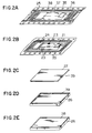
- a method of manufacturing the non-contact IC card according to this embodiment will be described with reference to Figs. 2A to 2E.
- a TAB board 25 on which a wiring pattern 37 is formed in the insulating film 35 is manufactured, the wiring pattern 37 including a coil 36.
- the insulating film 35 on which the TAB board 25 is formed is in the form of an elongated shape in such a manner that a plurality of the same wiring patterns 37 which respectively correspond to the IC cards are repeatedly formed on the insulating film 35.
- sprocket holes 38 are, at predetermined intervals, formed on the two side portions of the insulating film 35, the sprocket holes 38 acting to move the TAB board 25.
- the IC chip 21, the electronic parts 23 and the battery 24 are mounted on the TAB board 25.
- the thus mounted elements are electrically connected to the wiring pattern 37.
- the circuit portion of the non-contact IC card is formed. In this state, the circuit test can be carried out.
- the TAB board 25 is sealed up by the resin package 27 at the circuit portion of each of the IC cards before unnecessary portion are removed by cutting. As a result, a module 39 for the non-contact IC card is formed.
- the module 39 is, as shown in Fig. 2D, placed in the plastic package 26 before the module 39 is, from an upper portion, covered with the plastic panel 28 as shown in Fig. 2E.
- the non-contact IC card is manufactured.
- the module 39 is, according to this embodiment, wrapped with exterior members such as the plastic package 26 and the plastic panel 28, another structure may be employed which is arranged in such a manner that the module 39 is not wrapped by the exterior member but is used as the IC card as it is.
- the size of the module 39 may be arranged to be the size of the desired IC card.
- the thickness of an assembly in which an IC chip is mounted on an insulating film can be reduced to 0.5 mm or thereabouts.
- Insulating materials which can be used as insulating films in performing the invention include, by way of example only, polyimide films, glass-epoxy materials, and so on.
Landscapes
- Engineering & Computer Science (AREA)
- Computer Hardware Design (AREA)
- Microelectronics & Electronic Packaging (AREA)
- Physics & Mathematics (AREA)
- General Physics & Mathematics (AREA)
- Theoretical Computer Science (AREA)
- Computer Networks & Wireless Communication (AREA)
- Credit Cards Or The Like (AREA)
Description
- The present invention relates to a Tape-automated bonding (TAB) board manufactured by using the TAB technology and a non-contact IC card which uses the TAB board.
- Fig.3 illustrates the cross sectional shape of a conventional non-contact IC card. A TAB package 1 including an IC,
electronic parts 3 such as resistors and capacitors and abattery 4 serving as the power supply of this IC card are mounted on a printedboard 5. The above-described elements are respectively and electrically connected to a wiring pattern (omitted from the illustration) formed on the surface of the printedboard 5. The thus constituted printedboard 5 is accommodated in aplastic package 6 and is coated withresin 7. Furthermore, aplastic panel 8 serving as a cover of theplastic package 6 is disposed on theresin 7.Reference numeral 2 represents an outer lead of the TAB package 1. - Then, a method of manufacturing the conventional non-contact IC card constituted as shown in Fig. 3 will be described with reference to Figs. 4A to 4F. First, a TAB lead frame 10 as shown in Fig. 4A and having lead wires 9 arranged therein is manufactured. Then, an IC chip 11 is, as shown in Fig. 4B, mounted on the TAB lead frame 10. After the IC chip 11 has been sealed up with resin, unnecessary lead frame portions are removed by cutting and the
outer lead 2 is bent so that the TAB package 1 shown in Fig. 4C is manufactured. Then, the TAB package 1, thebattery 4 andelectronic parts 3 such as the resistors and capacitors are, as shown in Fig. 4D, mounted on the printedboard 5 on which acoil 12 is formed. Then, the printedboard 5 is placed in theplastic package 6 before the surface of the printedboard 5 is, as shown in Fig. 4E, sealed up with theresin 7. Furthermore, theplastic panel 8 serving as the cover is placed on theresin 7 so that the above-described conventional non-contact IC card is manufactured. - Since the conventional non-contact IC cards have been manufactured by the method as described above, there rises a problem in that the necessary number of the manufacturing processes is too large and the excessively long time and large labor are thereby necessary. What is even worse, since the printed
board 5 must be included, the thickness of the non-contact IC card cannot be reduced. Furthermore, as shown in Fig. 3, since the lower surface of the printedboard 5 is not sealed although the upper portion of the printedboard 5 is sealed up with resin, another problem rises in that the obtainable airtightness and the moisture resistance have not been satisfactory. - EP-A-0 376 062 discloses an electronic module for a small portable object. The module comprises a tape-automated bonding board, with electronic circuit components installed thereon. An annular coil is provided on the board in such a fashion as to encircle the circuit components. The coil is filled with resin and ultimately defines the module's outer wall. This arrangement does not overcome the above-described problems.
- Accordingly, an object of the present invention is to provide a module for an IC card with which a relatively thin non-contact IC card can be manufactured while decreasing the necessary number of the manufacturing processes.
- Another object of the present invention is to provide a reliable non-contact IC card which uses the module and the thickness of which can be reduced.
- With these objects in mind, the invention provides a module for a non-contact IC card as set out in
Claims 1 and 2 and a non-contact IC card as set out inClaims Claim 5 and a method for manufacturing an IC card as set out inClaim 6. - Since the TAB board according to the present invention is arranged in such a manner that the wiring pattern including the coil for transmitting data in a non-contact manner is formed on the insulating film, the printed board can be eliminated from the structure.
- Furthermore, the non-contact IC card according to the present invention is arranged in such a manner that the IC chip is mounted on the TAB board on which the coil is formed and is, as it is, sealed by the resin package.
-
- Fig. 1 is a cross sectional view which illustrates an embodiment of a non-contact IC card according to the present invention;
- Figs. 2A to 2E are perspective views which sequentially illustrate the method of manufacturing the non-contact IC card shown in Fig. 1;
- Fig. 3 is a cross sectional view which illustrates a conventional IC card; and
- Figs. 4A to 4F are perspective views which sequentially illustrate the method of manufacturing the non-contact IC card shown in Fig. 3.
- Preferred embodiments of the present invention will be described with reference to the drawings.
- Referring to Fig. 1, a non-contact IC card according to an embodiment of the present invention comprises a
TAB board 25 composed of aninsulating film 35 and a wiring pattern (omitted from the illustration) formed on theinsulating film 35. The wiring pattern includes acoil 36 spirally wound in the outer periphery of theinsulating film 35. Thecoil 36 acts to transmit data to and from an outer terminal equipment (omitted from the illustration) in a non-contact manner. - Furthermore, an
IC chip 21,electronic parts 23 such as resistors and capacitors and abattery 24 serving as the power supply of this non-contact IC card are mounted on theTAB board 25. The above-described elements are respectively and electrically connected to the unillustrated wiring pattern. The overall body of the thus formedTAB board 25 is sealed up by aresin package 27. Furthermore, aplastic package 26 and aplastic panel 28 are, as the exterior parts, formed so as to surround theresin package 27. - Then, a method of manufacturing the non-contact IC card according to this embodiment will be described with reference to Figs. 2A to 2E. First, as shown in Fig. 2A, a
TAB board 25 on which awiring pattern 37 is formed in theinsulating film 35 is manufactured, thewiring pattern 37 including acoil 36. Theinsulating film 35 on which theTAB board 25 is formed is in the form of an elongated shape in such a manner that a plurality of thesame wiring patterns 37 which respectively correspond to the IC cards are repeatedly formed on theinsulating film 35. Furthermore,sprocket holes 38 are, at predetermined intervals, formed on the two side portions of theinsulating film 35, thesprocket holes 38 acting to move theTAB board 25. - Then, as shown in Fig. 2B, the
IC chip 21, theelectronic parts 23 and thebattery 24 are mounted on theTAB board 25. The thus mounted elements are electrically connected to thewiring pattern 37. As a result, the circuit portion of the non-contact IC card is formed. In this state, the circuit test can be carried out. - Then, as shown in Fig. 2C, the
TAB board 25 is sealed up by theresin package 27 at the circuit portion of each of the IC cards before unnecessary portion are removed by cutting. As a result, amodule 39 for the non-contact IC card is formed. - Then, the
module 39 is, as shown in Fig. 2D, placed in theplastic package 26 before themodule 39 is, from an upper portion, covered with theplastic panel 28 as shown in Fig. 2E. Thus, the non-contact IC card is manufactured. - As described above, according to this embodiment, all of the elements are mounted on the
TAB board 25 so as to be sealed with the resin as it is. Therefore, a non-contact IC card the thickness of which can be reduced can be manufactured in a reduced number of manufacturing processes. Furthermore, since the circuit portion is perfectly sealed up in theresin package 27, the moisture resistance and the reliability can be improved. In addition, the circuit portions of a plurality of IC cards can be subjected to the circuit test while connecting the same to one another in a tape-like shape by the insulatingfilm 35. Therefore, the circuit test can be automated. - Although the
module 39 is, according to this embodiment, wrapped with exterior members such as theplastic package 26 and theplastic panel 28, another structure may be employed which is arranged in such a manner that themodule 39 is not wrapped by the exterior member but is used as the IC card as it is. In this case, the size of themodule 39 may be arranged to be the size of the desired IC card. - By the use of the invention, the thickness of an assembly in which an IC chip is mounted on an insulating film can be reduced to 0.5 mm or thereabouts.
- Insulating materials which can be used as insulating films in performing the invention include, by way of example only, polyimide films, glass-epoxy materials, and so on.
Claims (6)
- A module for a non-contact IC card, comprising:a tape-automated bonding board (25) defined by an insulating film (35) provided with a wiring pattern (37), provided on a first surface of the insulating film (35);a plurality of circuit components (21, 23, 24) mounted on the first surface of the insulating film (35);a coil (36) for transmitting data in a non-contact manner, mounted on the first surface of the insulating film (35); anda quantity of resin (27), covering the first surface of the insulating film (35) and the said circuit components (21, 23, 24) and wiring pattern (37) provided thereon;characterised in that the coil (36) is defined by part of the said wiring pattern (37); and the resin (27) completely encapsulates the said tape-automated bonding board (25) and the said circuit components (21, 23, 24), provided thereon.
- A module for a non-contact IC card according to Claim 1, wherein the said coil (36) is spirally wound in the outer periphery of the insulating film (35).
- A non-contact IC card comprising a module according to Claim 1 or 2, and further comprising an exterior housing (26, 28) surrounding the resin package (27).
- A non-contact IC card according to Claim 3, wherein the housing (26, 28) is made from plastic.
- A method of manufacturing a module for a non-contact IC card comprising:(i) mounting a plurality of electronic components (21, 23, 24) upon a tape-automated bonding board (25), formed from an insulating film (35) provided with a wiring pattern (37) including a non-contact coil (36), so as to electrically connect the electronic components (21, 23, 24) to the wiring pattern (37); and(ii) sealing the resulting structure in a package of resin (27).
- A method of manufacturing an IC card comprising forming a module in accordance with Claim 5 and(iii) placing the module (39) in a package (26); and(iv) covering the module (26) with a panel (28) to enclose it within the package (26).
Applications Claiming Priority (2)
| Application Number | Priority Date | Filing Date | Title |
|---|---|---|---|
| JP2276548A JPH04152191A (en) | 1990-10-17 | 1990-10-17 | Tab base and non-contact ic card using said tab base |
| JP276548/90 | 1990-10-17 |
Publications (3)
| Publication Number | Publication Date |
|---|---|
| EP0481776A2 EP0481776A2 (en) | 1992-04-22 |
| EP0481776A3 EP0481776A3 (en) | 1993-03-03 |
| EP0481776B1 true EP0481776B1 (en) | 1997-12-29 |
Family
ID=17571022
Family Applications (1)
| Application Number | Title | Priority Date | Filing Date |
|---|---|---|---|
| EP19910309570 Expired - Lifetime EP0481776B1 (en) | 1990-10-17 | 1991-10-17 | TAB board and non-contact IC card which uses the same |
Country Status (3)
| Country | Link |
|---|---|
| EP (1) | EP0481776B1 (en) |
| JP (1) | JPH04152191A (en) |
| DE (1) | DE69128517T2 (en) |
Cited By (4)
| Publication number | Priority date | Publication date | Assignee | Title |
|---|---|---|---|---|
| US7971339B2 (en) | 2006-09-26 | 2011-07-05 | Hid Global Gmbh | Method and apparatus for making a radio frequency inlay |
| US8286332B2 (en) | 2006-09-26 | 2012-10-16 | Hid Global Gmbh | Method and apparatus for making a radio frequency inlay |
| US8413316B2 (en) | 2007-09-18 | 2013-04-09 | Hid Global Ireland Teoranta | Method for bonding a wire conductor laid on a substrate |
| US8646675B2 (en) | 2004-11-02 | 2014-02-11 | Hid Global Gmbh | Laying apparatus, contact-making apparatus, movement system, laying and contact-making unit, production system, method for production and a transponder unit |
Families Citing this family (22)
| Publication number | Priority date | Publication date | Assignee | Title |
|---|---|---|---|---|
| AT400647B (en) * | 1992-05-20 | 1996-02-26 | Neutron Electronic Computer Gm | CARD WITH A MAGNETIC STRIP |
| FI94562C (en) * | 1992-11-09 | 1995-09-25 | Tapio Robertsson | Roller identification device and method for its manufacture |
| DE4311493C2 (en) * | 1993-04-07 | 2000-04-06 | Amatech Advanced Micromechanic | IC card module for producing an IC card |
| DE69323293T2 (en) * | 1993-04-14 | 1999-09-09 | Gustafson | Electronic marking device |
| DE4345473B4 (en) * | 1993-11-06 | 2006-03-23 | Ods Landis & Gyr Gmbh & Co. Kg | Contactless chip card, linked to scanner - has a structured laminated assembly which avoids tension peaks especially on bending |
| DE4337921C2 (en) * | 1993-11-06 | 1998-09-03 | Ods Gmbh & Co Kg | Contactless chip card with antenna coil |
| DE4345455B4 (en) * | 1993-11-06 | 2006-04-13 | Ods Landis & Gyr Gmbh & Co. Kg | Contactless chip card, linked to scanner - has a structured laminated assembly which avoids tension peaks especially on bending |
| JPH07220036A (en) * | 1994-02-04 | 1995-08-18 | Mitsubishi Electric Corp | Contactless semiconductor module |
| DE4410732C2 (en) * | 1994-03-28 | 1997-05-07 | Amatech Gmbh & Co Kg | Method for arranging a transponder unit having at least one chip and a wire coil on a substrate, as well as chip card with a correspondingly arranged transponder unit |
| US5528222A (en) * | 1994-09-09 | 1996-06-18 | International Business Machines Corporation | Radio frequency circuit and memory in thin flexible package |
| FR2724477B1 (en) * | 1994-09-13 | 1997-01-10 | Gemplus Card Int | NON-CONTACT CARD MANUFACTURING PROCESS |
| ES2120229T3 (en) * | 1994-09-30 | 1998-10-16 | Siemens Ag | SUPPORT PROVISION FOR INTEGRATION IN A CHIP CARD WITHOUT CONTACT. |
| JPH08230367A (en) * | 1994-12-27 | 1996-09-10 | Mitsubishi Electric Corp | Non-contact type ic card and its manufacturing method and apparatus |
| DE19525933C5 (en) * | 1995-07-17 | 2004-02-19 | Finn, David | Method and device for embedding a coil in the carrier substrate of an IC card |
| DE19529640A1 (en) * | 1995-08-11 | 1997-02-13 | Giesecke & Devrient Gmbh | Coil element for a data carrier with integrated circuit and non-contact coupling |
| DE19535324C1 (en) * | 1995-09-22 | 1997-01-23 | Siemens Ag | Chip card for access control system |
| FR2743649B1 (en) * | 1996-01-17 | 1998-04-03 | Gemplus Card Int | CONTACTLESS ELECTRONIC MODULE, ELECTRONIC LABEL CARD INCORPORATING THE SAME, AND METHODS OF MAKING SAME |
| US5786626A (en) * | 1996-03-25 | 1998-07-28 | Ibm Corporation | Thin radio frequency transponder with leadframe antenna structure |
| JP2002500794A (en) * | 1998-03-27 | 2002-01-08 | コーニンクレッカ フィリップス エレクトロニクス エヌ ヴィ | Data medium having a plug-in module mainly composed of a metal lead frame |
| DE10016037B4 (en) * | 2000-03-31 | 2005-01-05 | Interlock Ag | Method for producing a label or a chip card |
| DE50015958D1 (en) | 2000-05-05 | 2010-08-26 | Infineon Technologies Ag | smart card |
| JP5049959B2 (en) * | 2005-04-27 | 2012-10-17 | プリバシーズ,インコーポレイテッド | How to create low-loop adhesion for electronic cards, their manufacturing methods, smart cards, secure transaction cards, swipe emulating broadcasters and thin contouring applications |
Family Cites Families (5)
| Publication number | Priority date | Publication date | Assignee | Title |
|---|---|---|---|---|
| JPS61226888A (en) * | 1985-03-30 | 1986-10-08 | Anritsu Corp | Ic card |
| JPS6463197A (en) * | 1987-09-02 | 1989-03-09 | Hitachi Maxell | Ic card |
| JPH01157896A (en) * | 1987-09-28 | 1989-06-21 | Mitsubishi Electric Corp | Noncontact type ic card and noncontact type card reader writer |
| FR2641102B1 (en) * | 1988-12-27 | 1991-02-22 | Ebauchesfabrik Eta Ag | |
| JPH0494996A (en) * | 1990-08-10 | 1992-03-27 | Toshiba Corp | Ic card |
-
1990
- 1990-10-17 JP JP2276548A patent/JPH04152191A/en active Pending
-
1991
- 1991-10-17 EP EP19910309570 patent/EP0481776B1/en not_active Expired - Lifetime
- 1991-10-17 DE DE1991628517 patent/DE69128517T2/en not_active Expired - Fee Related
Cited By (4)
| Publication number | Priority date | Publication date | Assignee | Title |
|---|---|---|---|---|
| US8646675B2 (en) | 2004-11-02 | 2014-02-11 | Hid Global Gmbh | Laying apparatus, contact-making apparatus, movement system, laying and contact-making unit, production system, method for production and a transponder unit |
| US7971339B2 (en) | 2006-09-26 | 2011-07-05 | Hid Global Gmbh | Method and apparatus for making a radio frequency inlay |
| US8286332B2 (en) | 2006-09-26 | 2012-10-16 | Hid Global Gmbh | Method and apparatus for making a radio frequency inlay |
| US8413316B2 (en) | 2007-09-18 | 2013-04-09 | Hid Global Ireland Teoranta | Method for bonding a wire conductor laid on a substrate |
Also Published As
| Publication number | Publication date |
|---|---|
| JPH04152191A (en) | 1992-05-26 |
| EP0481776A3 (en) | 1993-03-03 |
| DE69128517T2 (en) | 1998-04-16 |
| EP0481776A2 (en) | 1992-04-22 |
| DE69128517D1 (en) | 1998-02-05 |
Similar Documents
| Publication | Publication Date | Title |
|---|---|---|
| EP0481776B1 (en) | TAB board and non-contact IC card which uses the same | |
| US5729894A (en) | Method of assembling ball bump grid array semiconductor packages | |
| US5273938A (en) | Method for attaching conductive traces to plural, stacked, encapsulated semiconductor die using a removable transfer film | |
| US6534711B1 (en) | Encapsulation package and method of packaging an electronic circuit module | |
| US5018051A (en) | IC card having circuit modules for mounting electronic components | |
| US5786626A (en) | Thin radio frequency transponder with leadframe antenna structure | |
| US5854740A (en) | Electronic circuit board with semiconductor chip mounted thereon, and manufacturing method therefor | |
| EP1168447A2 (en) | Multi-layered semiconductor device and method | |
| US4567545A (en) | Integrated circuit module and method of making same | |
| JP2000505242A (en) | Chip module and method of manufacturing chip module | |
| US4054938A (en) | Combined semiconductor device and printed circuit board assembly | |
| EP0506090A2 (en) | Semiconductor device with electromagnetic shield | |
| US5588202A (en) | Method for manufacturing an overmolded sensor | |
| US5504370A (en) | Electronic system circuit package directly supporting components on isolated subsegments | |
| US4907061A (en) | Electronic device | |
| JP2982286B2 (en) | Data carrier | |
| US5872026A (en) | Process of fabricating an integrated circuit die package having a plurality of pins | |
| US5470796A (en) | Electronic package with lead wire connections and method of making same | |
| US4491895A (en) | Decoupling capacitor and method of manufacture thereof | |
| US20050030723A1 (en) | Fully-molded or lidded circuit module assembly having edge-stiffening interlock features | |
| JPH0396266A (en) | Semiconductor integrated circuit module | |
| US6285561B1 (en) | Data carrier module device having integrated circuit and transmission coil connection contacts covered by a common protective cap | |
| EP1055193B1 (en) | Data carrier with chip and fully enclosed connection means | |
| KR100476669B1 (en) | Chip on board package and chip card using the same | |
| JPH03274021A (en) | Production of liquid crystal display device |
Legal Events
| Date | Code | Title | Description |
|---|---|---|---|
| PUAI | Public reference made under article 153(3) epc to a published international application that has entered the european phase |
Free format text: ORIGINAL CODE: 0009012 |
|
| AK | Designated contracting states |
Kind code of ref document: A2 Designated state(s): DE FR GB |
|
| PUAL | Search report despatched |
Free format text: ORIGINAL CODE: 0009013 |
|
| AK | Designated contracting states |
Kind code of ref document: A3 Designated state(s): DE FR GB |
|
| 17P | Request for examination filed |
Effective date: 19930901 |
|
| 17Q | First examination report despatched |
Effective date: 19951215 |
|
| GRAG | Despatch of communication of intention to grant |
Free format text: ORIGINAL CODE: EPIDOS AGRA |
|
| GRAH | Despatch of communication of intention to grant a patent |
Free format text: ORIGINAL CODE: EPIDOS IGRA |
|
| GRAH | Despatch of communication of intention to grant a patent |
Free format text: ORIGINAL CODE: EPIDOS IGRA |
|
| GRAA | (expected) grant |
Free format text: ORIGINAL CODE: 0009210 |
|
| AK | Designated contracting states |
Kind code of ref document: B1 Designated state(s): DE FR GB |
|
| REF | Corresponds to: |
Ref document number: 69128517 Country of ref document: DE Date of ref document: 19980205 |
|
| ET | Fr: translation filed | ||
| REG | Reference to a national code |
Ref country code: GB Ref legal event code: 727 |
|
| REG | Reference to a national code |
Ref country code: GB Ref legal event code: 727A |
|
| REG | Reference to a national code |
Ref country code: GB Ref legal event code: 727B |
|
| REG | Reference to a national code |
Ref country code: GB Ref legal event code: SP |
|
| PLBE | No opposition filed within time limit |
Free format text: ORIGINAL CODE: 0009261 |
|
| STAA | Information on the status of an ep patent application or granted ep patent |
Free format text: STATUS: NO OPPOSITION FILED WITHIN TIME LIMIT |
|
| 26N | No opposition filed | ||
| PGFP | Annual fee paid to national office [announced via postgrant information from national office to epo] |
Ref country code: FR Payment date: 19991011 Year of fee payment: 9 |
|
| PGFP | Annual fee paid to national office [announced via postgrant information from national office to epo] |
Ref country code: GB Payment date: 19991013 Year of fee payment: 9 |
|
| PGFP | Annual fee paid to national office [announced via postgrant information from national office to epo] |
Ref country code: DE Payment date: 19991018 Year of fee payment: 9 |
|
| PG25 | Lapsed in a contracting state [announced via postgrant information from national office to epo] |
Ref country code: GB Free format text: LAPSE BECAUSE OF NON-PAYMENT OF DUE FEES Effective date: 20001017 |
|
| GBPC | Gb: european patent ceased through non-payment of renewal fee |
Effective date: 20001017 |
|
| PG25 | Lapsed in a contracting state [announced via postgrant information from national office to epo] |
Ref country code: FR Free format text: LAPSE BECAUSE OF NON-PAYMENT OF DUE FEES Effective date: 20010629 |
|
| PG25 | Lapsed in a contracting state [announced via postgrant information from national office to epo] |
Ref country code: DE Free format text: LAPSE BECAUSE OF NON-PAYMENT OF DUE FEES Effective date: 20010703 |
|
| REG | Reference to a national code |
Ref country code: FR Ref legal event code: ST |