EP0480181B1 - Method and apparatus for batch processing of a semiconductor wafer - Google Patents
Method and apparatus for batch processing of a semiconductor wafer Download PDFInfo
- Publication number
- EP0480181B1 EP0480181B1 EP91115206A EP91115206A EP0480181B1 EP 0480181 B1 EP0480181 B1 EP 0480181B1 EP 91115206 A EP91115206 A EP 91115206A EP 91115206 A EP91115206 A EP 91115206A EP 0480181 B1 EP0480181 B1 EP 0480181B1
- Authority
- EP
- European Patent Office
- Prior art keywords
- set forth
- wafers
- process chamber
- pressure vessel
- pressure
- Prior art date
- Legal status (The legal status is an assumption and is not a legal conclusion. Google has not performed a legal analysis and makes no representation as to the accuracy of the status listed.)
- Expired - Lifetime
Links
Images


Classifications
-
- H—ELECTRICITY
- H01—ELECTRIC ELEMENTS
- H01L—SEMICONDUCTOR DEVICES NOT COVERED BY CLASS H10
- H01L21/00—Processes or apparatus adapted for the manufacture or treatment of semiconductor or solid state devices or of parts thereof
- H01L21/67—Apparatus specially adapted for handling semiconductor or electric solid state devices during manufacture or treatment thereof; Apparatus specially adapted for handling wafers during manufacture or treatment of semiconductor or electric solid state devices or components ; Apparatus not specifically provided for elsewhere
- H01L21/67005—Apparatus not specifically provided for elsewhere
- H01L21/67011—Apparatus for manufacture or treatment
- H01L21/67098—Apparatus for thermal treatment
- H01L21/67115—Apparatus for thermal treatment mainly by radiation
-
- C—CHEMISTRY; METALLURGY
- C30—CRYSTAL GROWTH
- C30B—SINGLE-CRYSTAL GROWTH; UNIDIRECTIONAL SOLIDIFICATION OF EUTECTIC MATERIAL OR UNIDIRECTIONAL DEMIXING OF EUTECTOID MATERIAL; REFINING BY ZONE-MELTING OF MATERIAL; PRODUCTION OF A HOMOGENEOUS POLYCRYSTALLINE MATERIAL WITH DEFINED STRUCTURE; SINGLE CRYSTALS OR HOMOGENEOUS POLYCRYSTALLINE MATERIAL WITH DEFINED STRUCTURE; AFTER-TREATMENT OF SINGLE CRYSTALS OR A HOMOGENEOUS POLYCRYSTALLINE MATERIAL WITH DEFINED STRUCTURE; APPARATUS THEREFOR
- C30B33/00—After-treatment of single crystals or homogeneous polycrystalline material with defined structure
- C30B33/005—Oxydation
-
- H—ELECTRICITY
- H01—ELECTRIC ELEMENTS
- H01L—SEMICONDUCTOR DEVICES NOT COVERED BY CLASS H10
- H01L21/00—Processes or apparatus adapted for the manufacture or treatment of semiconductor or solid state devices or of parts thereof
- H01L21/67—Apparatus specially adapted for handling semiconductor or electric solid state devices during manufacture or treatment thereof; Apparatus specially adapted for handling wafers during manufacture or treatment of semiconductor or electric solid state devices or components ; Apparatus not specifically provided for elsewhere
- H01L21/677—Apparatus specially adapted for handling semiconductor or electric solid state devices during manufacture or treatment thereof; Apparatus specially adapted for handling wafers during manufacture or treatment of semiconductor or electric solid state devices or components ; Apparatus not specifically provided for elsewhere for conveying, e.g. between different workstations
- H01L21/67763—Apparatus specially adapted for handling semiconductor or electric solid state devices during manufacture or treatment thereof; Apparatus specially adapted for handling wafers during manufacture or treatment of semiconductor or electric solid state devices or components ; Apparatus not specifically provided for elsewhere for conveying, e.g. between different workstations the wafers being stored in a carrier, involving loading and unloading
- H01L21/67766—Mechanical parts of transfer devices
-
- H—ELECTRICITY
- H01—ELECTRIC ELEMENTS
- H01L—SEMICONDUCTOR DEVICES NOT COVERED BY CLASS H10
- H01L21/00—Processes or apparatus adapted for the manufacture or treatment of semiconductor or solid state devices or of parts thereof
- H01L21/67—Apparatus specially adapted for handling semiconductor or electric solid state devices during manufacture or treatment thereof; Apparatus specially adapted for handling wafers during manufacture or treatment of semiconductor or electric solid state devices or components ; Apparatus not specifically provided for elsewhere
- H01L21/677—Apparatus specially adapted for handling semiconductor or electric solid state devices during manufacture or treatment thereof; Apparatus specially adapted for handling wafers during manufacture or treatment of semiconductor or electric solid state devices or components ; Apparatus not specifically provided for elsewhere for conveying, e.g. between different workstations
- H01L21/67763—Apparatus specially adapted for handling semiconductor or electric solid state devices during manufacture or treatment thereof; Apparatus specially adapted for handling wafers during manufacture or treatment of semiconductor or electric solid state devices or components ; Apparatus not specifically provided for elsewhere for conveying, e.g. between different workstations the wafers being stored in a carrier, involving loading and unloading
- H01L21/67778—Apparatus specially adapted for handling semiconductor or electric solid state devices during manufacture or treatment thereof; Apparatus specially adapted for handling wafers during manufacture or treatment of semiconductor or electric solid state devices or components ; Apparatus not specifically provided for elsewhere for conveying, e.g. between different workstations the wafers being stored in a carrier, involving loading and unloading involving loading and unloading of wafers
Definitions
- the lower space 57 (Fig. 2) below the cassettes 16 and below the bottom 56 of process chamber means 14 contain the air moving means and the power supply means required to operate the various components of apparatus 10.
- the entrance gate 20 for passing the cassettes 16 into compartment 12 is shown in Fig. 2 in horizontal alignment with the bottom row of cassettes 16, the xyz unit 32 not being shown in Fig. 2 to simplify the drawing.
- the fluid is allowed to bleed by gravity from the cylinder of device 84, thereby permitting lowering of closure 56 so that there is no need for driving the same downwardly under the influence of a drive fluid exerted on the upper end of the piston of element 84.
- Power input connector 122 and gas inlet 126 are shown in Fig. 11 in surrounding relationship to bell jar 95 having a steam inlet 129 and a steam outlet 132.
- a second power lead-in unit 122 can be provided.
- tubes 133 can be positioned around the outer periphery of bell jar 95 for containing thermocouples exteriorly of the bell jar for measuring the temperature in the vicinity of the outer surface of the bell jar. This temperature measurement provides a measure of the temperature of the steam or oxygen in the interior of the bell jar.
- the tower 45 containing a stack of semiconductor wafers 18 to be processed is then moved on to closure 56 when the same is lowered in the position thereof shown in Fig. 8.
- the closure 56 is elevated with the tower 45 thereon and with the bottom 115 of the bell jar supporting the tower as substantially shown in Fig. 18.
- Closure 56 is moved into the full line position thereof as shown in Fig. 8.
- Power device 72 (Fig. 6) is then energized to rotate the ring joint 74 relative to closure 56 so that bayonet means 70 will couple and lock the closure 56 to bottom ring 76.
- the seals are formed (Figs. 10 and 18) and bell jar closure 56 (Fig. 18) closes the bottom of the bell jar with the tower 45 in the bell jar as shown in Fig. 18.
- Typical process operations are Processes 1 and 2 shown in Tables 1 and 2 for a 50 wafer batch as follows: TABLE 1 PROCESS 1: 98,04 N/m 2 , 920°C, 460 nm (10 ATMOSPHERE, 920°C, 4600 ⁇ ) Step Time (Min) Temp °C N:m 2 Pressure (Atmos) Gas Standby -- 500 9,804 1 N 2 , 10LPM Push/Lock 3.0 500 9,804 1 N 2 + 1% O 2 Temp Ramp 17.0 500-920 9,804 1 N 2 + 1% O 2 Steam Purge 5.0 920 9,804 1 H 2 O, 8cc/min Pressures Ramp 5.0 920 9,804 ⁇ 98,04 1 ⁇ 10 H 2 O, 8cc/min Oxidation 14.0 920 98,04 10 H 2 O, 8cc/min Depress 5.0 920 98,04 ⁇ 2 10 ⁇ 1 None Anneal 20.0 920 9,804 1 N 2 Temp Ramp 17.0 920-500 9,
- the process chamber heaters are unique in heating process chamber 95 in that the entire chamber area is heated at a specific operating temperature. There is also rapid heat up due to high power graphite heaters and there is rapid cool down due to close proximity of the chill plate and a small thermal mass of the body of the bell jar.
- the heaters are of high impurity graphite to provide for no metallic contamination of the entire pressure vessel 11 or bell jar 94.
- the design of the bell jar is suitable for broad pressure ratings including a vacuum through 100 atmospheres.
- the steam generator is external to the process chamber so as to provide no contamination to the interior of the process chamber. Cold surfaces are eliminated to avoid silica deposits.
Landscapes
- Engineering & Computer Science (AREA)
- Condensed Matter Physics & Semiconductors (AREA)
- General Physics & Mathematics (AREA)
- Manufacturing & Machinery (AREA)
- Computer Hardware Design (AREA)
- Microelectronics & Electronic Packaging (AREA)
- Power Engineering (AREA)
- Physics & Mathematics (AREA)
- Chemical & Material Sciences (AREA)
- Health & Medical Sciences (AREA)
- Robotics (AREA)
- Toxicology (AREA)
- Crystallography & Structural Chemistry (AREA)
- Materials Engineering (AREA)
- Metallurgy (AREA)
- Organic Chemistry (AREA)
- Application Of Or Painting With Fluid Materials (AREA)
- Chemical Vapour Deposition (AREA)
Description
- This invention relates to improvements in the processing of semiconductor wafers and, more particularly, to a method and apparatus for the batch processing of a semiconductor wafer at a relatively high rate.
- The use of steam and fluid pressure to grow oxides on semiconductor wafers is well known and has been used extensively in the past. Typical temperatures of steam for this purpose are about 900 to 1,000°C, and fluid pressures are about 98,04 to 245,1 N/m2 (10 to 25 atmospheres). At these operating conditions, wafers in a batch can be processed at a moderate rate, such as less than 2 hours, an acceptable time period for profitable yield. Batch processing thus gives a high throughput while providing for acceptable process conditions.
- Because of the problems associated with conventional techniques of batch processing, a need exists for improvements in the batch processing of semiconductor wafers so that such processing can be more economically feasible. The present invention satisfies this need.
- Disclosures relating to the filed of the present invention include U.S. Patents 3,167,915, 4,268,538, 4,315,479 and 4,599,247. The method and apparatus to be described herein are improvements over the single wafer processing apparatus and method disclosed in U.S. Patent Application Serial No. 311,686, filed February 15, 1989, corresponding to EP 0 386 447.
- The present invention is directed to a method and apparatus for growing semiconductor quality, oxide thermal layers on semiconductor wafers. The primary object of the present invention is to provide an improved method and apparatus for batch processing semiconductor wafers, wherein the process is highly flexible and suitable for applying oxides to a plurality of wafers at a high throughput while achieving optimum process conditions. All aspects of the present invention cooperate for achieving acceptable process condition s while providing reasonable wafer throughput.
- Process speed is insured by high pressure and high temperature. For example, if the pressure is about 980,4 N/m2 (10 atmospheres, 150 psi) and at a temperature of 850°C, a time interval of approximately 7.0 minutes is required to grow a 150 nm (1,500Å) oxide layer on a wafer in a steam environment. The system can reach these operating conditions from ambient in approximately 27 minutes, and depressurization and cool-down require approximately 42 minutes.
- The apparatus of the present invention comprises a unique process chamber in a pressure vessel Loaded from the bottom, and the wafers are fed into the bottom of the process chamber under clean room conditions. The process chamber is adapted to be pressurized with an oxidant, such as high pressure steam or dry oxygen. The pressure vessel is adapted to be pressurized with an inert gas, such as nitrogen, to a high pressure.
- Another unique feature of the present invention is the use of a pressure control scheme which keeps the pressure vessel at a small positive pressure, such as 1 psi, relative to the pressure of the process chamber to insure hermetic integrity and cleanliness. The pressure control allows the apparatus of the present invention to be highly flexible, and capable of a wide range of operating conditions, such as from vacuum to high pressures, such as 245 N/m2 (25 atmospheres) and higher, and at temperatures ranging up to 900°C and higher.
- To obtain the required process rate and purity using the present invention, semiconductor wafers in a quartz tower or holder are placed in the process chamber in the pressure vessel, following which the process chamber is closed and pressurized with an oxidant, such as steam or dry oxygen. Heaters outside the process chamber are used to heat the interior of the process chamber. The steam is created and pressure is ramped at a certain rate, such as 206.840 N/m2 (30 psi) per minute. Since the walls of the process chamber must be relatively thin to minimize thermal cool-down, preventing breakage of the process chamber walls due to fluid pressure differential requires a unique chamber-vessel separation scheme which includes pressure equalization. Control of the fluid pressure in the process chamber and the pressure vessel is done electronically using pressure sensors and fluid valves.
- Steam is generated within a unique boiler at the upper end of and outside of the process chamber and within the pressure vessel. Steam flows into, through and out of the process chamber, and the steam exhausts through an exhaust tube which can form a part of the pressure equalization scheme. Other objects of this invention and the unique features of the invention apparent as the following specification progresses, reference being made to the accompanying drawings for an illustration of an embodiment of the invention.
-
- Fig. 1 is a top plan view, schematic in form and showing the xyz moving system for semiconductor wafers for placement in a process chamber within a pressure vessel;
- Fig. 2 is a side elevational view, generally schematic in form, of the combination of elements of Fig. 1, showing the vertical tower containing semiconductor wafers to be processed in a bottom loading process chamber;
- Fig. 3 is a view similar to Fig. 2 but showing the clean air flow from a plenum past the wafers in cassettes stacked adjacent to the process chamber in a clean room compartment and in the path of the air flow of the clean room atmosphere in which the process chamber is located;
- Fig. 4 is a perspective view, partly broken away and in section, showing the process chamber and a tower of semiconductor wafers about to be elevated into the process chamber as another tower of semiconductor wafers is being cooled;
- Fig. 5 is a view similar to Fig. 4 but showing another aspect view of the interior of the clean room compartment in which the cassettes of semiconductor wafers and the process chambers are located, the bottom of the process chamber being open;
- Fig. 6 is an elevational view of one side of the pressure vessel containing the process chamber with the bottom of the pressure vessel being closed;
- Fig. 7 is a rear elevational view of the combination of elements of Fig. 6;
- Fig. 8 is an elevational view of the opposite side of the pressure vessel with the lower closure of the pressure vessel being shown in dash lines in a lowered condition;
- Fig. 9 is a top plan view of the pressure vessel of Figs. 6-8;
- Figs. 9A and 9B are schematic diagrams of the fluid operating system of the apparatus of the present invention;
- Fig. 10 is a vertical section through the process chamber in the pressure vessel, the process chamber being formed by a bell jar of inert material, such as quartz, surrounded by heaters for heating a tower of semiconductor wafers to be placed into the bell jar;
- Fig. 11 is a horizontal section through the process chamber and pressure vessel of Fig. 10;
- Fig. 12 is a plan view of a planar graphite heater placed at the upper or lower end of the bell jar for heating the semiconductor wafers in the bell jar;
- Fig. 13 is a front elevational view of the chill plate assembly for the bottom of the bell jar for cooling the same;
- Fig. 14 is a bottom plan view of the fluid passages of the chill plate near the upper end of the bell jar;
- Fig. 15 is a cross-sectional view taken along line 15-15 of Fig. 14;
- Fig. 16 is a top plan view of the steam generator on the bell jar forming the process chamber of the present invention;
- Fig. 17 is a side elevational view of the steam generator of Fig. 16;
- Fig. 17A is a vertical section through the steam generator of Figs. 16 and 17; and
- Fig. 18 is a vertical section through the process chamber and the pressure vessel, showing the tower of semiconductor wafers mounted in the bell jar and the bottom closure of the bell jar in place.
- The apparatus for the batch processing of semiconductor wafers is broadly denoted by the numeral 10 and includes means defining a closed
compartment 12 for housing pressure vessel means 11 containing process chamber means 14. A plurality of cassettes or boats 16 (Figs. 2-5) which include stacks ofsemiconductor wafers 18 which are moved incassettes 16 intocompartment 12 through an access opening 20 adjacent to avideo display 22 and acontrol panel 24 for use in moving thecassettes 16 about incompartment 12. - The means defining closed
compartment 12 includecorner posts 26 which have panels associated with them to presentplenum chambers 28 and Hepa filters 30. Thus,compartment 12 can be provided with clean room characteristics of the highest quality. - An
xyz moving unit 32 is located incompartment 12 adjacent to pressure vessel means 11 shown in Fig. 1. Thex part 34 ofunit 32 moves thecassettes 16 along the length ofpart 34 in an x direction, in the direction of arrows 35. Ay part 36 moves thex part 34 in a y direction, in the direction ofarrows 38, and az part 40 is movable upwardly and downwardly and has a pair ofhorizontal legs 43 which are to be placed through thehandle 44 of aquartz tower 45, the tower being adapted to support a plurality of vertically spaced semiconductor wafers to be processed which move with the tower into process chamber means 14 through the bottom thereof. - A
shiftable arm 46 has a pair of spaced fingers 48 (Fig. 1) andarm 46 is coupled with control means 50 coupled withunit 32 whereby the operation ofparts xyz unit 32 operate to move thearm 46 relative to thecassette 16. Thefingers 48 ofarm 46 also support asemiconductor wafer 18, as the wafer is moved from acassette 16 toward and intotower 45 in preparation for filling the tower with wafers to be processed. Another control means 47 is provided incompartment 12 for centering eachwafer 18 on a turntable 49 (Fig. 1) so that the wafer will be properly oriented relative totower 45 as the wafer is being moved byarm 46 into a respective horizontal position intower 45. This centering of the wafer avoids scraping the edge of the wafer on the tower during insertion of the wafer, thereby avoiding the formation of particles which would contaminate the atmosphere surrounding the wafer. - Means 50 also operates to rotate the
arm 46 about thecentral axis 51 of an elongated shaft-like element 52 coupled witharm 46. The purpose of rotating thearm 46 is to move the arm out of tight places near thetower 45 whensemiconductor wafers 18 are moved into and out of thetower 45 before and after processing of the wafers in the process chamber means 14. - Fig. 2 shows
compartment 12 withcassettes 16 containingsemiconductor wafers 18 to be processed, the cassettes being supported onshelves 53 adjacent to one side 55 of the housing defining thecompartment 12. Thecassettes 16 are also adjacent to tower 45 containingsemiconductor wafers 18 which are to be placed on thebottom closure 56 as shown in Fig. 2, the tower being denoted bynumeral 45 and handle 44 is at the upper end of the tower. Asecond tower 45a is abovetower 45 and in a position for cooling thewafers 18 after the wafers have been processed and moved removed from the process chamber means 14. - The lower space 57 (Fig. 2) below the
cassettes 16 and below the bottom 56 of process chamber means 14 contain the air moving means and the power supply means required to operate the various components of apparatus 10. Theentrance gate 20 for passing thecassettes 16 intocompartment 12 is shown in Fig. 2 in horizontal alignment with the bottom row ofcassettes 16, thexyz unit 32 not being shown in Fig. 2 to simplify the drawing. -
XYZ unit 32 is shown in Fig. 3 adjacent topressure vessel 11 and removed from a vertical stack ofcassettes 16 forsemiconductor wafers 18 to be processed in process chamber means 14. The air flow fromplenum 28 through aHepa filter 30 is indicated byair flow arrows 60 toward and through thecassettes 16 to provide for the clean room characteristics ofcompartment 12 at all times. - Fig. 4 is a view showing the pressure vessel means 11 open with the
bottom closure 56 in a lowered condition and afirst tower 45 ofsemiconductor wafers 18 being supported onclosure 56 before the closure is elevated into a position closing the bottom of pressure vessel means 11. Fig. 4 also shows a pair offingers 43 forming parts ofxyz unit 32 and adapted to be inserted into the handle 44 (Figs. 1-3) ofwafer tower 45 to facilitate the movement of the tower onto and off the center pedestal 56a ofclosure 56. The other wafer tower being denoted by numeral 45a and being above acassette 16 ofsemiconductor wafers 18 which are to be taken one by one out of the cassette and placed intotower 45a.Other cassettes 16 are shown schematically in Fig. 4 in standby positions, waiting movement by the xyz means 32 in the positions, such as the position shown belowtower 45a so that thesemiconductor wafers 18 from thestandby cassettes 16 can be transferred into positions intower 45a. Fig. 4 also shows the access opening 20 by means of which cassettes 16 can be moved intocompartment 12 and into the standby position shown in Fig. 4. - Fig. 5 shows the entrance opening 20 adjacent to the access opening 21 by means of which cassettes 16 of
semiconductor wafers 18 can be moved intocompartment 12. Fig. 5 also shows the pressure vessel means 11 as being open with theclosure 56 thereof lowered into a position adjacent to thebottom surface 59 of the compartment. - Fig. 5 clearly shows
arm 46 carried by xyzunit 32 and the arm is shown transferring asemiconductor wafer 18 from acassette 16 to tower 45. Spinning means 47, 48 (Fig. 1) is provided for eachwafer 18, respectively, so that when the wafer is positioned byarm 46 in the correspondingtower 45, the wafer will be properly centered so that the wafer will not scrape the tower walls and generate particles. Also,arm 46 has an optical device 46a (Fig. 1) to optically find the slots of thetower 45 to avoid scraping of the wafer during insertion. - Pressure vessel means 11 is carried on the upper ends of a pair of spaced, generally
vertical posts 64 and 66 (Fig. 7), posts 64 and 66 being mounted onfeet 68 for attachment to the bottom surface of thehousing containing compartment 12. -
Closure 56 comprises acylindrical member 59 which supportstower 45 at the upper end of the vessel and which is coupled by a bayonet connection 70 (Figs. 6 and 7), on the upper marginal edge ofclosure 56. A fluid piston and cylinder assembly 72 (Fig. 6) is adapted to engage and to be connected at one end thereof to the ring joint 74. The opposite end ofassembly 72 is connected to one of theposts joint member 76 provided with bayonet connection means 70 thereon. Once theclosure 56 is in the elevated position shown in Figs. 6-8,device 72 is energized to rotate ring joint 74 relative toclosure 56 so that the bayonet connection 70 will connectclosure 56 and joint 74 together, thereby closing and sealingclosure 56 to the lower ring of ring joint 74. Before this occurs, thetower 45 ofsemiconductor wafers 18 will be moved into a bell jar defining process chamber means 14 by the actuation of one or more fluid actuated power devices 77 (Fig. 6 and 8). Actuation ofdevice 77 also forces a pair of fluid seals into engagement with each other, these seals being shown in Figs. 10 and 18 and described hereinafter. Whentower 45 is supported in reaction chamber means 14, steam and a gas under pressure, such as nitrogen, will be charged into the pressure vessel and the process chamber means, respectively, for effecting the processing of the semiconductor wafers in the tower within the process chamber means. - A pair of side supports 80 and 82 are coupled (Figs. 6-8) with
closure 56 on opposite sides hereof.Supports posts closure 56 upwardly and downwardly. - A fluid piston cylinder assembly 84 (Figs. 7 and 8) is coupled at its upper end to a fixed support 86 and at its lower end to a
bracket 88 on one of thesupports cylinder assembly 84 is used to elevatesupports Closure 56 is moved from the dashed line position of Fig. 8, to the full line position closing the lower end of the process chamber andpressure vessel 11. Means (not shown) is provided to supply a fluid under pressure to the cylinder ofdevice 84 to thereby activate the same and draw the piston upwardly to thereby raiseclosure member 56 to the full line position thereof shown in Fig. 8. Tolower closure 56 relative to thepressure vessel 11, the fluid is allowed to bleed by gravity from the cylinder ofdevice 84, thereby permitting lowering ofclosure 56 so that there is no need for driving the same downwardly under the influence of a drive fluid exerted on the upper end of the piston ofelement 84. - Fig. 9 shows pressure vessel means 11 with
posts track 67 for guiding thesupports closure 56 relative topressure vessel 11. - Figs. 9A and 9B show a schematic of the fluid operating system of apparatus 10.
- The fluid system of Figs. 9A and 9B include a
deionized water inlet 90 with aline 91 connected to adeionized water channel 92 having avalve 93 coupled to asteam generator 94 on the upper end of abell jar 95 defining aprocess chamber 96 into which atower 45 ofsemiconductor wafers 18 is placed. Steam from the generator enteredprocess chamber 96 and oxidizes the semiconductor wafers in the process chamber. The steam exhaust follows along line 97 and passes outwardly along a line 98 (Fig. 9B). - A fluid input 98 (Fig. 9A) is provided for the flow of nitrogen or other inert gas, which flows through a high pressure gas panel denoted by the numeral 99 (Fig. 9A) and then through a pressure monitor 100 (Fig. 9B) before the nitrogen reaches the
pressure vessel 11 along the line 101 (Fig. 9b). - An oxygen input 103 can be provided in case oxygen is to be used as the oxidant instead of steam. A chloride-based material, such as HCL, can be provided at an input 104 to a
cleaning subsystem 105 for cleaning purposes.Exhaust system 106 is provided for exhausting gasses to the atmosphere along theline 107 as desired or deemed necessary. Anexhaust line 108 is provided for the HCL after it is used for cleaning purposes. - In Fig. 10,
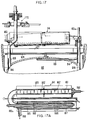
pressure vessel 11 includes a circular top 110 secured in any suitable manner to the upper end 111 of a double walledhousing having walls Bell jar 95 is located withinpressure vessel 11 and is surrounded by a cylindrical heater means 114 so as to heat the interior of the bell jar and thereby the semiconductor wafers on the tower (Fig. 18) in the bell jar. Heater means 114 can be comprised of two or more parts which are cylindrical and which encircle the outer surface of the bell jar. Suitable electrical connections can be quickly and easily made to the heater means to supply electrical power thereto. - The bell jar is made of thin walled inert material, such as quartz, that has a bottom 115 (Fig. 18) which is curved as shown in Fig. 18 and which has an angular, downwardly extending part 116 (Fig. 10) and a horizontal,
annular part 117 provided with anannular seal 118 engaged with the bottom surface of aflange 119 on the bottom ofbell jar 95. Aseal 120 engages betweenflange 119 andflange 121 onwall 113 ofpressure vessel 11. The twoflanges openings 118 and 120 (Fig. 10). These seals are forced into engagement with each other when power device 77 (Figs. 6 and 8) is actuated. - Feed through
connectors 122 and 123 (Fig. 10) are carried bypressure vessel 11 to provide power leads to the interior ofpressure vessel 11 for energizingheaters 114 and the other heaters, such as upperplanar heater 124 above the bell jar and lowerplanar heater 125 below bottom 56 (Fig. 18). Afluid inlet device 126 and afluid outlet device 127 are provided to direct an inert gas, such as nitrogen, into the interior ofpressure vessel 11 and around thebell jar 95. - Upper and
lower chill plates heater 124 and directly belowheater 125, respectively (Fig. 10).Steam inlet 129 extends into the bell jar through an opening 130 (Fig. 10) and has a loweropen end 131 near the bottom 115 of the bell jar as shown in Fig. 18. -
Power input connector 122 andgas inlet 126 are shown in Fig. 11 in surrounding relationship tobell jar 95 having asteam inlet 129 and asteam outlet 132. A second power lead-inunit 122 can be provided. Moreover,tubes 133 can be positioned around the outer periphery ofbell jar 95 for containing thermocouples exteriorly of the bell jar for measuring the temperature in the vicinity of the outer surface of the bell jar. This temperature measurement provides a measure of the temperature of the steam or oxygen in the interior of the bell jar. -
Planar heaters 124 and 125 (Fig. 10) takes the shape of the heater shown in Fig. 12 with the heater having a plurality of parallel segments which are in the same plane, the segments being denoted by the numeral 124a in Fig. 12 and the segments being coupled together at their ends to form a single segment of a predetermined length and secured toterminals 140 and 141 to which electrical power is supplied for energizing the heaters.Quartz standoff ribs 142 are provided to keep the segments of the heaters out of physical contact with adjacent structure, such as thechill plate 128 adjacent to heater 125 (Fig. 10), thestandoff quartz members 142 being shown in Fig. 13 as being engageable with the upper surface of thechill plate 128. -
Fluid lines 144 are provided to supply coolant to chillplates 128 which are tubular as shown in Fig. 14 for receiving coolant at oneend 146 and the coolant flows through the various passages denoted bynumerals 147 and out of theoutlet 148 back to a reservoir for further chilling operations before it returns to the chill plates. The quartz standoff members are also shown in Fig. 14 and thefluid passages 147 are shown in thechill blades 128 of Fig. 15. -
Steam generator 94 is shown in Figs. 16, 17 and 17A. The steam generator is adjacent to and above the upper or top 95a of thebell jar 95. Thesteam generator 94 includes an inlet tube 160 (Fig. 16) for receiving deionized water entering the steam generator and movable through a passage 161 (Fig. 17A) past baffles 162 which define a serpentine path for the deionized water. If oxygen is the oxidant, it is input attube 160a (Figs. 17 and 17A). Heater means 163 surroundspassage 161 and superheats the deionized water to form steam at a first pressure. This steam continues aroundpassage 164 and into atube 165 which hasopenings 166 therethrough communicating with anouter tube 167 surrounded by heater means 169 for superheating the steam to a second temperature and pressure. Theouter tube 167 is coupled to asteam outlet 168 which is connected to line 129 (Fig. 10) where the superheated steam passes into the bell jar and enters the bell jar at exit opening 131 (Fig. 18). The steam exits from the bell jar along line 169 (Fig. 17) and equalization means 170 can be provided to equalize the pressure of the steam in the bell jar with the nitrogen on the exterior of the bell jar. In this way, thin walled quartz bell jars can be used in the present invention. - Apparatus 10 is first prepared for operation by directing
cassettes 16 ofsemiconductor wafers 18 into compartment 12 (Fig. 1-5), the wafers to be subjected to steam and high pressure steam or oxygen, or mixtures of steam and oxygen for processing the wafer. - The
wafers 18 from acassette 16 are transferred by xyz means 32 into aquartz tower 45 of the type shown in Fig. 18 and the tower is lifted byhandle 44 ontoclosure 56 which carries bottom 115 (Fig. 18) of the bell jar. - The
tower 45 containing a stack ofsemiconductor wafers 18 to be processed is then moved on toclosure 56 when the same is lowered in the position thereof shown in Fig. 8. By actuation of fluid activateddevice 84, theclosure 56 is elevated with thetower 45 thereon and with the bottom 115 of the bell jar supporting the tower as substantially shown in Fig. 18.Closure 56 is moved into the full line position thereof as shown in Fig. 8. Power device 72 (Fig. 6) is then energized to rotate the ring joint 74 relative toclosure 56 so that bayonet means 70 will couple and lock theclosure 56 tobottom ring 76. When this occurs, the seals are formed (Figs. 10 and 18) and bell jar closure 56 (Fig. 18) closes the bottom of the bell jar with thetower 45 in the bell jar as shown in Fig. 18. - Quartz seals will be made at O-
ring seals 118 and 120 (Fig. 10), and steam from thesteam generator 94 is then formed and directed into the interior of the bell jar. Nitrogen under pressure is then directed intopressure vessel 11. The pressure of the nitrogen is at a slight positive pressure relative to the pressure of the steam in the process chamber, and the pressures of the steam and nitrogen are controlled by electronic means so that the pressure of the steam inside the bell jar is slightly less (1%) than the gas pressure of the nitrogen outside the bell jar. Thus, the bell jar wall can be relatively thin without fear of breakage of the bell jar. This feature reduces the cost of the bell jar and simplifies the handling thereof because of the reduced weight. This feature also improves heat conduction. - Typical process operations are Processes 1 and 2 shown in Tables 1 and 2 for a 50 wafer batch as follows:
TABLE 1 PROCESS 1: 98,04 N/m2, 920°C, 460 nm (10 ATMOSPHERE, 920°C, 4600Å) Step Time (Min) Temp °C N:m2 Pressure (Atmos) Gas Standby -- 500 9,804 1 N2, 10LPM Push/Lock 3.0 500 9,804 1 N2 + 1% O2 Temp Ramp 17.0 500-920 9,804 1 N2 + 1% O2 Steam Purge 5.0 920 9,804 1 H2O, 8cc/min Pressures Ramp 5.0 920 9,804→98,04 1→10 H2O, 8cc/min Oxidation 14.0 920 98,04 10 H2O, 8cc/min Depress 5.0 920 98,04→2 10→1 None Anneal 20.0 920 9,804 1 N2 Temp Ramp 17.0 920-500 9,804 1 N2 Unload 3.0 500 9,804 1 N2 Tower Transfer TOTAL PROCESS TIME = 90 MINUTES TABLE 2 PROCESS 2: 98,04 N/m2, 850°C, 150 nm (10 ATMOSPHERE, 850°C, 1500Å) Step Time (Min) Temp °C Pressure (Atmos) Gas Standby -- 500 9,804 1 N2, 10LPM Push/Lock 3.0 500 9,804 1 N2 + 1% O2 Temp Ramp 14.0 500-850 9,804 1 N2 + 1% O2 Steam Purge 5.0 850 9,804 1 H2O, 8cc/min Pressures Ramp 5.0 850 9,804→98,04 1→10 H2O, 8cc/min Oxidation 7.0 850 98,04 10 H2O, 8cc/min Depress 5.0 850 98,04→9,804 10→1 None Anneal 20.0 850 9,804 1 N2 Temp Ramp 14.0 850-500 9,804 1 N2 Unload 3.0 500 9,804 1 N2 Tower Transfer TOTAL PROCESS TIME = 80 MINUTES - Once the process is complete, both the steam and nitrogen are exhausted to the atmosphere through the steam outlet and the gas outlets shown in Fig. 9B. No significant pressure differential across the quartz walls of
bell jar 95 is generated during this cycle so that no breakage is experienced. - The entire steam generator is high purity material, such as quartz, to prevent contamination of the interior of the process chamber of the bell jar to thereby avoid contamination of wafers in the
process chamber 95. The construction of the steam generator is such as to prevent water drops from enteringprocess chamber 95. - The heaters for the steam generator are of high purity material, such as graphite, and provide for minimal metal contamination to the quartz material of the steam generator.
- The process chamber heaters are unique in
heating process chamber 95 in that the entire chamber area is heated at a specific operating temperature. There is also rapid heat up due to high power graphite heaters and there is rapid cool down due to close proximity of the chill plate and a small thermal mass of the body of the bell jar. The heaters are of high impurity graphite to provide for no metallic contamination of theentire pressure vessel 11 orbell jar 94. The design of the bell jar is suitable for broad pressure ratings including a vacuum through 100 atmospheres. - The process chamber of the present invention has a low thermal mass so as to provide fast response time in carrying out the processes achievable with use of the process chamber. There is no metallic contamination associated with the process chamber and the heaters surrounding the process chamber are graphite heaters, thus adding to the no metallic contamination feature of the present invention. There are no ceramic members or fiber insulators, and the minimal particle generators are used throughout the system.
- The process chamber is designed for a 60-wafer tower includes 50 process wafers and a number of guard and test wafers. A separate steam generator is provided for the process chamber and the semiconductor wafers are heated and cooled inside the process chamber itself. The wafers are surrounded by heaters having no cold ends. Greater temperature control is achieved with the heaters of the present invention. There is minimal convection of the heat from the heaters and better oxide uniformity is achieved with such heaters. There is also minimal white power deposits.
- There is optimum contamination control with the system of the present invention. To this end, the heaters are high purity graphite with no ceramic insulation, no vestibule blocks, no quartz wool, and no Kanthal (heavy metal source). The heaters are completely isolated from the wafers.
- The steam generator is external to the process chamber so as to provide no contamination to the interior of the process chamber. Cold surfaces are eliminated to avoid silica deposits.
- The wafers are in the process chamber during temperature ramp up and ramp down. Generally, the process carried out by the method and apparatus of the present invention is a low temperature process, such as in the range of 600°C to 700°C with reasonable throughput, and minimal diffusion of implanted species. The laminar flow achievable with the system of the present invention reduces particle contamination of the wafers. Another process which can be carried out with the system of the present invention is the reflow process.
- The laminar flow in the apparatus of the present invention is horizontal flow and the wafers are all horizontal in the compartment exteriorly of the process chamber and within the process chamber. All laminar flow in the compartment is directed into the mouth of each wafer cassette. There is no oblique flow at the corners of the cassettes. Any potential particle generator is individually exhausted and all mechanisms are downstream of the wafers in the compartment.
Claims (39)
- Apparatus (10) for processing semiconductor wafers comprising:a pressure vessel (11) ;a hollow body (95) within the pressure vessel and having a process chamber (14), said pressure vessel (11) and said body (95) having respective openings for receiving a first semiconductor wafer (18) as part of a plurality of wafers moving as a unit from a location (12) outside the pressure vessel (11) to a location within the process chamber (14);actuatable means (56, 70, 72, 74, 77, 80, 82) coupled with and shiftable relative to the pressure vessel (11) for closing the openings;means (94; 103) coupled with the body for directing an oxidant at high pressure into the process chamber (14);means (101) for directing an inert gas under pressure into the pressure vessel;means (114, 124) for heating the oxidant in the process chamber;means (127, 128) for cooling the body after the first wafer in the process chamber has been processed; andmeans coupled with the pressure vessel and the body for equilibrating pressures of the inert gas and the oxidant and for substantially isolating the inert gas from the oxidant;characterized in thatsaid actuatable means (56, 70, 72, 74, 77, 80, 82) is shiftable vertically (80, 82) relative to the pressure vessel (11) for closing the openings, said openings are lower openings and are adapted to receive said first semiconductor wafer as part of a plurality of wafers moving as a unit from a location below said pressure vessel.
- Apparatus as set forth in Claim 1, wherein said body (95) is bell jar-shaped and formed of an inert material.
- Apparatus as set forth in Claim 1, wherein said means for directing an oxidant into the process chamber includes a steam generator (94) having a fluid inlet (160), and a source of deionized water coupled to the inlet of the steam generator.
- Apparatus as set forth in Claim 3, wherein the steam generator (94) includes a tube having a fluid inlet (160) and baffle (162) means for forming a serpentine path for fluid flow through the tube.
- Apparatus as set forth in Claim 4, wherein said tube (160) and the baffle means (162) are formed of an inert material.
- Apparatus as set fort in Claim 4, wherein is included a heater (163) surrounding the tube for heating deionized water flowing through the tube.
- Apparatus as set forth in Claim 4, wherein said steam generator (94) includes a second tube (165) coupled to the first tube, and a third tube (167) surrounding the second tube, there being holes (166) in the second tube for placing the second and third tubes (167) in fluid communication with each other, there being a heater (163) surrounding the third tube.
- Apparatus as set forth in Claim 7, wherein the holes (166) are in the upper extremity of the second tube.
- Apparatus as set forth in Claim 7, wherein the third tube (167) is provided with means (131) for placing the third tube (167) in fluid communication with the process chamber (95).
- Apparatus as set forth in Claim 7, wherein the second and third tube (166,167) are formed of an inert material.
- Apparatus as set forth in Claim 1, wherein said oxidant heating means (119,124) includes a heater within the pressure vessel (11) and in proximity to and outside said body (95) for heating the interior of the process chamber.
- Apparatus as set forth in Claim 11, wherein said heater means includes a pair of planar heaters (124,125) above (124) and below (125) the body.
- Apparatus as set forth in Claim 12, wherein said body has an upper wall and a lower wall, said planar heaters (124,125) being adjacent to respective upper and lower walls.
- Apparatus as set forth in Claim 1, wherein said cooling means (127,128) includes a chill plate adjacent to the body.
- Apparatus as set forth in Claim 12, wherein said body includes an upper wall and a lower wall, said cooling means includes an upper chill plate (127) and a lower chill plate (128) near respective upper an lower walls, and means (144) coupling the chill plates to a source of coolant.
- Apparatus as set forth in Claim 1, wherein said equilibrating and isolating means includes electronic circuitry (100) and valve means for controlling steam and gas flow to the body and pressure vessel, respectively.
- Apparatus as set forth in Claim 16, wherein is included seal means (70, 74) between the closing means and the body (11) for sealing the junction therebetween when said closing means is actuated.
- Apparatus as set forth in Claim 1, wherein said closing means (56,70,72,74,77,80,82) includes a pair of closure members (56,74) within the pressure vessel and movable upwardly into closing relationship to the lower openings of the pressure vessel and the body, respectively, and means for moving the closure members vertically into and out of the operative positions thereof.
- Apparatus as set forth in Claim 16, wherein said means for moving the closure members includes a fluid-actuated power device (77) below the pressure vessel.
- Apparatus as set forth in Claim 1, wherein is included a steam generator (94) in the pressure vessel (11), said generator (94) being operable to pressurize the process chamber (11) to a pressure of at least 980,392 N/m2 (100 atmospheres), and means for supplying the inert gas to the interior of the pressure vessel at a pressure of at least 980,392 N/m2 (100 atmospheres).
- Apparatus as set forth in Claim 1, wherein is included means for heating the steam in the process chamber to a temperature in the range of 600°C to 1100°C.
- Apparatus as set forth in Claim 19 wherein said temperature is 600°C to 1100°C,
- A method for processing a plurality of semiconductor wafers comprising:forming a first space (11) surrounding a second space (95) with the spaces having lower openings;inserting a plurality of semiconductor wafers (18) in the first and second spaces upwards through the lower openings;closing the lower openings to the atmosphere;directing an inert gas under pressure into the first space (11);directing into the second space (95) an oxidant under pressure;heating the wafers (18) to a processing temperature;cooling the wafers (18) in the second space after the wafers have been processed; andequilibrating the pressures in the first (11) and second (95) spaces while substantially isolating the spaces from each other.
- A method as set forth in Claim 23, wherein said inert gas is nitrogen and the oxidant is a gas taken from the group including steam and oxygen.
- A method as set forth in Claim 23, wherein the fluid pressure of the first and second spaces during processing of the wafers is in the range of a vacuum to 98,04 to 245,1 N/m (10 to 25 atmospheres).
- A method as set forth in Claim 23, wherein the fluid pressure in said spaces is approximately 980,392 N/m2 (100 atmospheres).
- A method as set forth in Claim 23, wherein the processing temperature is in the range of 0°C to 1100°C.
- A method as set forth in Claim 23, wherein the processing temperature is in the range of 600°C to 1000°C.
- A method as set forth in Claim 23, wherein the processing temperature is approximately 900°C and the fluid pressure in the spaces is approximately 98,04 to 245 N/m2 (10 to 25 atmospheres).
- A method as set forth in Claim 23, wherein the step of filling the second space with an oxidant includes generating steam in a region within the first space (11) and externally of the second space (95).
- A method as set forth in Claim 30, wherein said generating step includes moving deionized water along a serpentine path as the water (18) is being heated to steam.
- A method as set forth in Claim 23, wherein is included the step of preventing water from entering the second space as the steam is being generated.
- A method as set forth in Claim 23, wherein said equilibrating step includes preventing the oxidant from entering the first space (11) and substantially preventing the inert gas from entering the second space (95), whereby the pressure of one space balances or exceeds the pressure in the other space.
- A method as set forth in Claim 33, wherein the steps of heating the wafers (18) and cooling the wafers (18) are performed when the wafers are in the second space (95).
- A method as set forth in Claim 23, wherein is included the step of creating an air flow along a horizontal path, and positioning the wafers (18) and cassettes (16) at the upstream ends of the path to minimize the particle contamination, and keeping the downstream end of the path substantially free of structure.
- A method as set forth in Claim 23, wherein said step of heating the wafers includes energizing graphite heaters (124,125).
- Apparatus as set forth in Claim 1, wherein said heating means (124,125) includes a number of graphite heaters.
- Apparatus as set forth in Claim 1, wherein said heating means (124,125) includes means for ramping the temperature upwardly in the process chamber, said cooling means (127,128) including means for ramping the cooling of the body downwardly, said heating means (124,125) and cooling means (127,128) being operable to heat the wafers and for cooling the wafers when the wafers are in the process chamber (95).
- Apparatus as set fort in Claim 1, wherein is included air flow means for directing an air flow along a horizontal path, said wafers (18) initially being in cassettes (16) in horizontal positions in the cassettes, said cassettes (16) being near the upstream end of the air flow means to minimize or substantially eliminate Particle contamination.
Applications Claiming Priority (2)
| Application Number | Priority Date | Filing Date | Title |
|---|---|---|---|
| US590402 | 1990-09-28 | ||
| US07/590,402 US5167716A (en) | 1990-09-28 | 1990-09-28 | Method and apparatus for batch processing a semiconductor wafer |
Publications (3)
| Publication Number | Publication Date |
|---|---|
| EP0480181A2 EP0480181A2 (en) | 1992-04-15 |
| EP0480181A3 EP0480181A3 (en) | 1992-04-22 |
| EP0480181B1 true EP0480181B1 (en) | 1996-06-12 |
Family
ID=24362115
Family Applications (1)
| Application Number | Title | Priority Date | Filing Date |
|---|---|---|---|
| EP91115206A Expired - Lifetime EP0480181B1 (en) | 1990-09-28 | 1991-09-09 | Method and apparatus for batch processing of a semiconductor wafer |
Country Status (4)
| Country | Link |
|---|---|
| US (1) | US5167716A (en) |
| EP (1) | EP0480181B1 (en) |
| JP (1) | JP3069412B2 (en) |
| DE (1) | DE69120193T2 (en) |
Families Citing this family (400)
| Publication number | Priority date | Publication date | Assignee | Title |
|---|---|---|---|---|
| US5578132A (en) * | 1993-07-07 | 1996-11-26 | Tokyo Electron Kabushiki Kaisha | Apparatus for heat treating semiconductors at normal pressure and low pressure |
| US5880041A (en) * | 1994-05-27 | 1999-03-09 | Motorola Inc. | Method for forming a dielectric layer using high pressure |
| US5611898A (en) * | 1994-12-08 | 1997-03-18 | International Business Machines Corporation | Reaction chamber having in situ oxygen generation |
| US6002109A (en) * | 1995-07-10 | 1999-12-14 | Mattson Technology, Inc. | System and method for thermal processing of a semiconductor substrate |
| US6030902A (en) * | 1996-02-16 | 2000-02-29 | Micron Technology Inc | Apparatus and method for improving uniformity in batch processing of semiconductor wafers |
| US5653808A (en) * | 1996-08-07 | 1997-08-05 | Macleish; Joseph H. | Gas injection system for CVD reactors |
| DE69710655T2 (en) * | 1996-08-07 | 2002-10-31 | Concept Systems Design Inc | Gas supply system for CVD reactors |
| US5846888A (en) * | 1996-09-27 | 1998-12-08 | Micron Technology, Inc. | Method for in-situ incorporation of desirable impurities into high pressure oxides |
| US5679585A (en) * | 1996-11-15 | 1997-10-21 | Advanced Micro Devices, Inc. | Method for forming metal silicide on a semiconductor surface with minimal effect on pre-existing implants |
| TW539918B (en) | 1997-05-27 | 2003-07-01 | Tokyo Electron Ltd | Removal of photoresist and photoresist residue from semiconductors using supercritical carbon dioxide process |
| TW589391B (en) * | 1997-07-08 | 2004-06-01 | Unaxis Trading Ag | Process for vacuum treating workpieces, and corresponding process equipment |
| CH692741A5 (en) * | 1997-07-08 | 2002-10-15 | Unaxis Trading Ltd C O Balzers | Vacuum processing system for work piece |
| US6391377B1 (en) * | 1997-07-08 | 2002-05-21 | Unaxis Balzers Aktiengesellschaft | Process for vacuum treating workpieces, and corresponding process equipment |
| US6158449A (en) * | 1997-07-17 | 2000-12-12 | Tokyo Electron Limited | Cleaning and drying method and apparatus |
| EP1209721B1 (en) * | 1997-10-10 | 2007-12-05 | European Community | Inductive type plasma processing chamber |
| TW489827U (en) | 1998-04-09 | 2002-06-01 | Kobe Steel Ltd | Apparatus for high-temperature and high-pressure treatment of semiconductor substrates |
| JP3445148B2 (en) * | 1998-05-21 | 2003-09-08 | 株式会社神戸製鋼所 | High-temperature and high-pressure processing equipment for substrates to be processed |
| JP2000277521A (en) * | 1999-03-26 | 2000-10-06 | Kobe Steel Ltd | Method and apparatus of high-temperature high-pressure treatment for semiconductor wafer |
| JP3268446B2 (en) * | 1999-04-07 | 2002-03-25 | 科学技術振興事業団 | Substrate heating device |
| US6334266B1 (en) | 1999-09-20 | 2002-01-01 | S.C. Fluids, Inc. | Supercritical fluid drying system and method of use |
| US6508259B1 (en) * | 1999-08-05 | 2003-01-21 | S.C. Fluids, Inc. | Inverted pressure vessel with horizontal through loading |
| US6748960B1 (en) | 1999-11-02 | 2004-06-15 | Tokyo Electron Limited | Apparatus for supercritical processing of multiple workpieces |
| WO2001033615A2 (en) | 1999-11-02 | 2001-05-10 | Tokyo Electron Limited | Method and apparatus for supercritical processing of multiple workpieces |
| JP4724353B2 (en) | 2000-07-26 | 2011-07-13 | 東京エレクトロン株式会社 | High pressure processing chamber for semiconductor substrates |
| US7001468B1 (en) | 2002-02-15 | 2006-02-21 | Tokyo Electron Limited | Pressure energized pressure vessel opening and closing device and method of providing therefor |
| US7387868B2 (en) | 2002-03-04 | 2008-06-17 | Tokyo Electron Limited | Treatment of a dielectric layer using supercritical CO2 |
| KR100863782B1 (en) * | 2002-03-08 | 2008-10-16 | 도쿄엘렉트론가부시키가이샤 | Substrate processing apparatus and substrate processing method |
| JP2003282457A (en) * | 2002-03-26 | 2003-10-03 | Hitachi Kokusai Electric Inc | Method of manufacturing semiconductor device |
| US7021635B2 (en) * | 2003-02-06 | 2006-04-04 | Tokyo Electron Limited | Vacuum chuck utilizing sintered material and method of providing thereof |
| US7225820B2 (en) * | 2003-02-10 | 2007-06-05 | Tokyo Electron Limited | High-pressure processing chamber for a semiconductor wafer |
| US7077917B2 (en) | 2003-02-10 | 2006-07-18 | Tokyo Electric Limited | High-pressure processing chamber for a semiconductor wafer |
| US7270137B2 (en) | 2003-04-28 | 2007-09-18 | Tokyo Electron Limited | Apparatus and method of securing a workpiece during high-pressure processing |
| US7163380B2 (en) | 2003-07-29 | 2007-01-16 | Tokyo Electron Limited | Control of fluid flow in the processing of an object with a fluid |
| US20050035514A1 (en) * | 2003-08-11 | 2005-02-17 | Supercritical Systems, Inc. | Vacuum chuck apparatus and method for holding a wafer during high pressure processing |
| US20050067002A1 (en) * | 2003-09-25 | 2005-03-31 | Supercritical Systems, Inc. | Processing chamber including a circulation loop integrally formed in a chamber housing |
| US7186093B2 (en) * | 2004-10-05 | 2007-03-06 | Tokyo Electron Limited | Method and apparatus for cooling motor bearings of a high pressure pump |
| US7250374B2 (en) | 2004-06-30 | 2007-07-31 | Tokyo Electron Limited | System and method for processing a substrate using supercritical carbon dioxide processing |
| US7307019B2 (en) | 2004-09-29 | 2007-12-11 | Tokyo Electron Limited | Method for supercritical carbon dioxide processing of fluoro-carbon films |
| US20060065189A1 (en) * | 2004-09-30 | 2006-03-30 | Darko Babic | Method and system for homogenization of supercritical fluid in a high pressure processing system |
| US7491036B2 (en) | 2004-11-12 | 2009-02-17 | Tokyo Electron Limited | Method and system for cooling a pump |
| US7140393B2 (en) | 2004-12-22 | 2006-11-28 | Tokyo Electron Limited | Non-contact shuttle valve for flow diversion in high pressure systems |
| US7434590B2 (en) | 2004-12-22 | 2008-10-14 | Tokyo Electron Limited | Method and apparatus for clamping a substrate in a high pressure processing system |
| US7435447B2 (en) | 2005-02-15 | 2008-10-14 | Tokyo Electron Limited | Method and system for determining flow conditions in a high pressure processing system |
| US7291565B2 (en) | 2005-02-15 | 2007-11-06 | Tokyo Electron Limited | Method and system for treating a substrate with a high pressure fluid using fluorosilicic acid |
| US7767145B2 (en) | 2005-03-28 | 2010-08-03 | Toyko Electron Limited | High pressure fourier transform infrared cell |
| US7380984B2 (en) * | 2005-03-28 | 2008-06-03 | Tokyo Electron Limited | Process flow thermocouple |
| US20060225772A1 (en) * | 2005-03-29 | 2006-10-12 | Jones William D | Controlled pressure differential in a high-pressure processing chamber |
| US7494107B2 (en) | 2005-03-30 | 2009-02-24 | Supercritical Systems, Inc. | Gate valve for plus-atmospheric pressure semiconductor process vessels |
| US7789971B2 (en) | 2005-05-13 | 2010-09-07 | Tokyo Electron Limited | Treatment of substrate using functionalizing agent in supercritical carbon dioxide |
| US7524383B2 (en) | 2005-05-25 | 2009-04-28 | Tokyo Electron Limited | Method and system for passivating a processing chamber |
| US20070187386A1 (en) | 2006-02-10 | 2007-08-16 | Poongsan Microtec Corporation | Methods and apparatuses for high pressure gas annealing |
| JP5014709B2 (en) | 2006-08-28 | 2012-08-29 | 日揮触媒化成株式会社 | Method for forming low dielectric constant amorphous silica coating and low dielectric constant amorphous silica coating obtained by the method |
| US8986456B2 (en) | 2006-10-10 | 2015-03-24 | Asm America, Inc. | Precursor delivery system |
| KR101354140B1 (en) | 2008-02-27 | 2014-01-22 | 소이텍 | Thermalization of gaseous precursors in cvd reactors |
| US10378106B2 (en) | 2008-11-14 | 2019-08-13 | Asm Ip Holding B.V. | Method of forming insulation film by modified PEALD |
| US9394608B2 (en) * | 2009-04-06 | 2016-07-19 | Asm America, Inc. | Semiconductor processing reactor and components thereof |
| US8802201B2 (en) | 2009-08-14 | 2014-08-12 | Asm America, Inc. | Systems and methods for thin-film deposition of metal oxides using excited nitrogen-oxygen species |
| US8883270B2 (en) | 2009-08-14 | 2014-11-11 | Asm America, Inc. | Systems and methods for thin-film deposition of metal oxides using excited nitrogen—oxygen species |
| US8877655B2 (en) | 2010-05-07 | 2014-11-04 | Asm America, Inc. | Systems and methods for thin-film deposition of metal oxides using excited nitrogen-oxygen species |
| US8809096B1 (en) * | 2009-10-22 | 2014-08-19 | Stion Corporation | Bell jar extraction tool method and apparatus for thin film photovoltaic materials |
| US9312155B2 (en) | 2011-06-06 | 2016-04-12 | Asm Japan K.K. | High-throughput semiconductor-processing apparatus equipped with multiple dual-chamber modules |
| US9793148B2 (en) | 2011-06-22 | 2017-10-17 | Asm Japan K.K. | Method for positioning wafers in multiple wafer transport |
| US10364496B2 (en) | 2011-06-27 | 2019-07-30 | Asm Ip Holding B.V. | Dual section module having shared and unshared mass flow controllers |
| US10854498B2 (en) | 2011-07-15 | 2020-12-01 | Asm Ip Holding B.V. | Wafer-supporting device and method for producing same |
| US20130023129A1 (en) | 2011-07-20 | 2013-01-24 | Asm America, Inc. | Pressure transmitter for a semiconductor processing environment |
| DE102011083245B4 (en) * | 2011-09-22 | 2019-04-25 | Siltronic Ag | Method and device for depositing an epitaxial layer of silicon on a semiconductor wafer of monocrystalline silicon by vapor deposition in a process chamber |
| US9096931B2 (en) | 2011-10-27 | 2015-08-04 | Asm America, Inc | Deposition valve assembly and method of heating the same |
| US9341296B2 (en) | 2011-10-27 | 2016-05-17 | Asm America, Inc. | Heater jacket for a fluid line |
| US9017481B1 (en) | 2011-10-28 | 2015-04-28 | Asm America, Inc. | Process feed management for semiconductor substrate processing |
| US9167625B2 (en) | 2011-11-23 | 2015-10-20 | Asm Ip Holding B.V. | Radiation shielding for a substrate holder |
| US9005539B2 (en) * | 2011-11-23 | 2015-04-14 | Asm Ip Holding B.V. | Chamber sealing member |
| US9202727B2 (en) | 2012-03-02 | 2015-12-01 | ASM IP Holding | Susceptor heater shim |
| US8946830B2 (en) | 2012-04-04 | 2015-02-03 | Asm Ip Holdings B.V. | Metal oxide protective layer for a semiconductor device |
| US9029253B2 (en) | 2012-05-02 | 2015-05-12 | Asm Ip Holding B.V. | Phase-stabilized thin films, structures and devices including the thin films, and methods of forming same |
| US8728832B2 (en) | 2012-05-07 | 2014-05-20 | Asm Ip Holdings B.V. | Semiconductor device dielectric interface layer |
| US8933375B2 (en) | 2012-06-27 | 2015-01-13 | Asm Ip Holding B.V. | Susceptor heater and method of heating a substrate |
| US9558931B2 (en) | 2012-07-27 | 2017-01-31 | Asm Ip Holding B.V. | System and method for gas-phase sulfur passivation of a semiconductor surface |
| US9117866B2 (en) | 2012-07-31 | 2015-08-25 | Asm Ip Holding B.V. | Apparatus and method for calculating a wafer position in a processing chamber under process conditions |
| US9659799B2 (en) | 2012-08-28 | 2017-05-23 | Asm Ip Holding B.V. | Systems and methods for dynamic semiconductor process scheduling |
| US9169975B2 (en) | 2012-08-28 | 2015-10-27 | Asm Ip Holding B.V. | Systems and methods for mass flow controller verification |
| US9021985B2 (en) | 2012-09-12 | 2015-05-05 | Asm Ip Holdings B.V. | Process gas management for an inductively-coupled plasma deposition reactor |
| US9324811B2 (en) | 2012-09-26 | 2016-04-26 | Asm Ip Holding B.V. | Structures and devices including a tensile-stressed silicon arsenic layer and methods of forming same |
| US10714315B2 (en) | 2012-10-12 | 2020-07-14 | Asm Ip Holdings B.V. | Semiconductor reaction chamber showerhead |
| US9640416B2 (en) | 2012-12-26 | 2017-05-02 | Asm Ip Holding B.V. | Single-and dual-chamber module-attachable wafer-handling chamber |
| US8894870B2 (en) | 2013-02-01 | 2014-11-25 | Asm Ip Holding B.V. | Multi-step method and apparatus for etching compounds containing a metal |
| US20160376700A1 (en) | 2013-02-01 | 2016-12-29 | Asm Ip Holding B.V. | System for treatment of deposition reactor |
| US9589770B2 (en) | 2013-03-08 | 2017-03-07 | Asm Ip Holding B.V. | Method and systems for in-situ formation of intermediate reactive species |
| US9484191B2 (en) | 2013-03-08 | 2016-11-01 | Asm Ip Holding B.V. | Pulsed remote plasma method and system |
| US8993054B2 (en) | 2013-07-12 | 2015-03-31 | Asm Ip Holding B.V. | Method and system to reduce outgassing in a reaction chamber |
| US9018111B2 (en) | 2013-07-22 | 2015-04-28 | Asm Ip Holding B.V. | Semiconductor reaction chamber with plasma capabilities |
| US9793115B2 (en) | 2013-08-14 | 2017-10-17 | Asm Ip Holding B.V. | Structures and devices including germanium-tin films and methods of forming same |
| US9396934B2 (en) | 2013-08-14 | 2016-07-19 | Asm Ip Holding B.V. | Methods of forming films including germanium tin and structures and devices including the films |
| US9240412B2 (en) | 2013-09-27 | 2016-01-19 | Asm Ip Holding B.V. | Semiconductor structure and device and methods of forming same using selective epitaxial process |
| US9556516B2 (en) | 2013-10-09 | 2017-01-31 | ASM IP Holding B.V | Method for forming Ti-containing film by PEALD using TDMAT or TDEAT |
| US9605343B2 (en) | 2013-11-13 | 2017-03-28 | Asm Ip Holding B.V. | Method for forming conformal carbon films, structures conformal carbon film, and system of forming same |
| US10179947B2 (en) | 2013-11-26 | 2019-01-15 | Asm Ip Holding B.V. | Method for forming conformal nitrided, oxidized, or carbonized dielectric film by atomic layer deposition |
| US10683571B2 (en) | 2014-02-25 | 2020-06-16 | Asm Ip Holding B.V. | Gas supply manifold and method of supplying gases to chamber using same |
| US10167557B2 (en) | 2014-03-18 | 2019-01-01 | Asm Ip Holding B.V. | Gas distribution system, reactor including the system, and methods of using the same |
| US9447498B2 (en) | 2014-03-18 | 2016-09-20 | Asm Ip Holding B.V. | Method for performing uniform processing in gas system-sharing multiple reaction chambers |
| US11015245B2 (en) | 2014-03-19 | 2021-05-25 | Asm Ip Holding B.V. | Gas-phase reactor and system having exhaust plenum and components thereof |
| US9404587B2 (en) | 2014-04-24 | 2016-08-02 | ASM IP Holding B.V | Lockout tagout for semiconductor vacuum valve |
| US10858737B2 (en) | 2014-07-28 | 2020-12-08 | Asm Ip Holding B.V. | Showerhead assembly and components thereof |
| US9543180B2 (en) | 2014-08-01 | 2017-01-10 | Asm Ip Holding B.V. | Apparatus and method for transporting wafers between wafer carrier and process tool under vacuum |
| US9890456B2 (en) | 2014-08-21 | 2018-02-13 | Asm Ip Holding B.V. | Method and system for in situ formation of gas-phase compounds |
| WO2016052023A1 (en) * | 2014-09-30 | 2016-04-07 | 株式会社日立国際電気 | Semiconductor production device, semiconductor-device production method, and recording medium |
| US10941490B2 (en) | 2014-10-07 | 2021-03-09 | Asm Ip Holding B.V. | Multiple temperature range susceptor, assembly, reactor and system including the susceptor, and methods of using the same |
| US9657845B2 (en) | 2014-10-07 | 2017-05-23 | Asm Ip Holding B.V. | Variable conductance gas distribution apparatus and method |
| KR102300403B1 (en) | 2014-11-19 | 2021-09-09 | 에이에스엠 아이피 홀딩 비.브이. | Method of depositing thin film |
| KR102263121B1 (en) | 2014-12-22 | 2021-06-09 | 에이에스엠 아이피 홀딩 비.브이. | Semiconductor device and manufacuring method thereof |
| US9478415B2 (en) | 2015-02-13 | 2016-10-25 | Asm Ip Holding B.V. | Method for forming film having low resistance and shallow junction depth |
| US10529542B2 (en) | 2015-03-11 | 2020-01-07 | Asm Ip Holdings B.V. | Cross-flow reactor and method |
| US10276355B2 (en) | 2015-03-12 | 2019-04-30 | Asm Ip Holding B.V. | Multi-zone reactor, system including the reactor, and method of using the same |
| US10458018B2 (en) | 2015-06-26 | 2019-10-29 | Asm Ip Holding B.V. | Structures including metal carbide material, devices including the structures, and methods of forming same |
| US10600673B2 (en) | 2015-07-07 | 2020-03-24 | Asm Ip Holding B.V. | Magnetic susceptor to baseplate seal |
| US9899291B2 (en) | 2015-07-13 | 2018-02-20 | Asm Ip Holding B.V. | Method for protecting layer by forming hydrocarbon-based extremely thin film |
| US10043661B2 (en) | 2015-07-13 | 2018-08-07 | Asm Ip Holding B.V. | Method for protecting layer by forming hydrocarbon-based extremely thin film |
| US10083836B2 (en) | 2015-07-24 | 2018-09-25 | Asm Ip Holding B.V. | Formation of boron-doped titanium metal films with high work function |
| US10087525B2 (en) | 2015-08-04 | 2018-10-02 | Asm Ip Holding B.V. | Variable gap hard stop design |
| US9647114B2 (en) | 2015-08-14 | 2017-05-09 | Asm Ip Holding B.V. | Methods of forming highly p-type doped germanium tin films and structures and devices including the films |
| US9711345B2 (en) | 2015-08-25 | 2017-07-18 | Asm Ip Holding B.V. | Method for forming aluminum nitride-based film by PEALD |
| US9960072B2 (en) | 2015-09-29 | 2018-05-01 | Asm Ip Holding B.V. | Variable adjustment for precise matching of multiple chamber cavity housings |
| US9909214B2 (en) | 2015-10-15 | 2018-03-06 | Asm Ip Holding B.V. | Method for depositing dielectric film in trenches by PEALD |
| US10211308B2 (en) | 2015-10-21 | 2019-02-19 | Asm Ip Holding B.V. | NbMC layers |
| US10322384B2 (en) | 2015-11-09 | 2019-06-18 | Asm Ip Holding B.V. | Counter flow mixer for process chamber |
| US9455138B1 (en) | 2015-11-10 | 2016-09-27 | Asm Ip Holding B.V. | Method for forming dielectric film in trenches by PEALD using H-containing gas |
| US9905420B2 (en) | 2015-12-01 | 2018-02-27 | Asm Ip Holding B.V. | Methods of forming silicon germanium tin films and structures and devices including the films |
| US9607837B1 (en) | 2015-12-21 | 2017-03-28 | Asm Ip Holding B.V. | Method for forming silicon oxide cap layer for solid state diffusion process |
| US9735024B2 (en) | 2015-12-28 | 2017-08-15 | Asm Ip Holding B.V. | Method of atomic layer etching using functional group-containing fluorocarbon |
| US9627221B1 (en) | 2015-12-28 | 2017-04-18 | Asm Ip Holding B.V. | Continuous process incorporating atomic layer etching |
| US11139308B2 (en) | 2015-12-29 | 2021-10-05 | Asm Ip Holding B.V. | Atomic layer deposition of III-V compounds to form V-NAND devices |
| US10529554B2 (en) | 2016-02-19 | 2020-01-07 | Asm Ip Holding B.V. | Method for forming silicon nitride film selectively on sidewalls or flat surfaces of trenches |
| US10468251B2 (en) | 2016-02-19 | 2019-11-05 | Asm Ip Holding B.V. | Method for forming spacers using silicon nitride film for spacer-defined multiple patterning |
| US9754779B1 (en) | 2016-02-19 | 2017-09-05 | Asm Ip Holding B.V. | Method for forming silicon nitride film selectively on sidewalls or flat surfaces of trenches |
| US10501866B2 (en) | 2016-03-09 | 2019-12-10 | Asm Ip Holding B.V. | Gas distribution apparatus for improved film uniformity in an epitaxial system |
| US10343920B2 (en) | 2016-03-18 | 2019-07-09 | Asm Ip Holding B.V. | Aligned carbon nanotubes |
| US9892913B2 (en) | 2016-03-24 | 2018-02-13 | Asm Ip Holding B.V. | Radial and thickness control via biased multi-port injection settings |
| US10865475B2 (en) | 2016-04-21 | 2020-12-15 | Asm Ip Holding B.V. | Deposition of metal borides and silicides |
| US10087522B2 (en) | 2016-04-21 | 2018-10-02 | Asm Ip Holding B.V. | Deposition of metal borides |
| US10190213B2 (en) | 2016-04-21 | 2019-01-29 | Asm Ip Holding B.V. | Deposition of metal borides |
| US10032628B2 (en) | 2016-05-02 | 2018-07-24 | Asm Ip Holding B.V. | Source/drain performance through conformal solid state doping |
| US10367080B2 (en) | 2016-05-02 | 2019-07-30 | Asm Ip Holding B.V. | Method of forming a germanium oxynitride film |
| KR102592471B1 (en) | 2016-05-17 | 2023-10-20 | 에이에스엠 아이피 홀딩 비.브이. | Method of forming metal interconnection and method of fabricating semiconductor device using the same |
| US11453943B2 (en) | 2016-05-25 | 2022-09-27 | Asm Ip Holding B.V. | Method for forming carbon-containing silicon/metal oxide or nitride film by ALD using silicon precursor and hydrocarbon precursor |
| US10388509B2 (en) | 2016-06-28 | 2019-08-20 | Asm Ip Holding B.V. | Formation of epitaxial layers via dislocation filtering |
| US10612137B2 (en) | 2016-07-08 | 2020-04-07 | Asm Ip Holdings B.V. | Organic reactants for atomic layer deposition |
| US9859151B1 (en) | 2016-07-08 | 2018-01-02 | Asm Ip Holding B.V. | Selective film deposition method to form air gaps |
| US9793135B1 (en) | 2016-07-14 | 2017-10-17 | ASM IP Holding B.V | Method of cyclic dry etching using etchant film |
| US10714385B2 (en) | 2016-07-19 | 2020-07-14 | Asm Ip Holding B.V. | Selective deposition of tungsten |
| US10381226B2 (en) | 2016-07-27 | 2019-08-13 | Asm Ip Holding B.V. | Method of processing substrate |
| US9887082B1 (en) | 2016-07-28 | 2018-02-06 | Asm Ip Holding B.V. | Method and apparatus for filling a gap |
| US10395919B2 (en) | 2016-07-28 | 2019-08-27 | Asm Ip Holding B.V. | Method and apparatus for filling a gap |
| US9812320B1 (en) | 2016-07-28 | 2017-11-07 | Asm Ip Holding B.V. | Method and apparatus for filling a gap |
| KR102532607B1 (en) | 2016-07-28 | 2023-05-15 | 에이에스엠 아이피 홀딩 비.브이. | Substrate processing apparatus and method of operating the same |
| US10177025B2 (en) | 2016-07-28 | 2019-01-08 | Asm Ip Holding B.V. | Method and apparatus for filling a gap |
| US10090316B2 (en) | 2016-09-01 | 2018-10-02 | Asm Ip Holding B.V. | 3D stacked multilayer semiconductor memory using doped select transistor channel |
| US10410943B2 (en) | 2016-10-13 | 2019-09-10 | Asm Ip Holding B.V. | Method for passivating a surface of a semiconductor and related systems |
| US10643826B2 (en) | 2016-10-26 | 2020-05-05 | Asm Ip Holdings B.V. | Methods for thermally calibrating reaction chambers |
| US11532757B2 (en) | 2016-10-27 | 2022-12-20 | Asm Ip Holding B.V. | Deposition of charge trapping layers |
| US10229833B2 (en) | 2016-11-01 | 2019-03-12 | Asm Ip Holding B.V. | Methods for forming a transition metal nitride film on a substrate by atomic layer deposition and related semiconductor device structures |
| US10643904B2 (en) | 2016-11-01 | 2020-05-05 | Asm Ip Holdings B.V. | Methods for forming a semiconductor device and related semiconductor device structures |
| US10435790B2 (en) | 2016-11-01 | 2019-10-08 | Asm Ip Holding B.V. | Method of subatmospheric plasma-enhanced ALD using capacitively coupled electrodes with narrow gap |
| US10714350B2 (en) | 2016-11-01 | 2020-07-14 | ASM IP Holdings, B.V. | Methods for forming a transition metal niobium nitride film on a substrate by atomic layer deposition and related semiconductor device structures |
| US10134757B2 (en) | 2016-11-07 | 2018-11-20 | Asm Ip Holding B.V. | Method of processing a substrate and a device manufactured by using the method |
| KR102546317B1 (en) | 2016-11-15 | 2023-06-21 | 에이에스엠 아이피 홀딩 비.브이. | Gas supply unit and substrate processing apparatus including the same |
| US10340135B2 (en) | 2016-11-28 | 2019-07-02 | Asm Ip Holding B.V. | Method of topologically restricted plasma-enhanced cyclic deposition of silicon or metal nitride |
| KR20180068582A (en) | 2016-12-14 | 2018-06-22 | 에이에스엠 아이피 홀딩 비.브이. | Substrate processing apparatus |
| US11447861B2 (en) | 2016-12-15 | 2022-09-20 | Asm Ip Holding B.V. | Sequential infiltration synthesis apparatus and a method of forming a patterned structure |
| US11581186B2 (en) | 2016-12-15 | 2023-02-14 | Asm Ip Holding B.V. | Sequential infiltration synthesis apparatus |
| US9916980B1 (en) | 2016-12-15 | 2018-03-13 | Asm Ip Holding B.V. | Method of forming a structure on a substrate |
| KR20180070971A (en) | 2016-12-19 | 2018-06-27 | 에이에스엠 아이피 홀딩 비.브이. | Substrate processing apparatus |
| US10269558B2 (en) | 2016-12-22 | 2019-04-23 | Asm Ip Holding B.V. | Method of forming a structure on a substrate |
| US10867788B2 (en) | 2016-12-28 | 2020-12-15 | Asm Ip Holding B.V. | Method of forming a structure on a substrate |
| US11390950B2 (en) | 2017-01-10 | 2022-07-19 | Asm Ip Holding B.V. | Reactor system and method to reduce residue buildup during a film deposition process |
| US10655221B2 (en) | 2017-02-09 | 2020-05-19 | Asm Ip Holding B.V. | Method for depositing oxide film by thermal ALD and PEALD |
| US10468261B2 (en) | 2017-02-15 | 2019-11-05 | Asm Ip Holding B.V. | Methods for forming a metallic film on a substrate by cyclical deposition and related semiconductor device structures |
| WO2018150536A1 (en) * | 2017-02-17 | 2018-08-23 | 株式会社Kokusai Electric | Substrate processing device, semiconductor device manufacturing method, and program |
| US10529563B2 (en) | 2017-03-29 | 2020-01-07 | Asm Ip Holdings B.V. | Method for forming doped metal oxide films on a substrate by cyclical deposition and related semiconductor device structures |
| US10283353B2 (en) | 2017-03-29 | 2019-05-07 | Asm Ip Holding B.V. | Method of reforming insulating film deposited on substrate with recess pattern |
| US10103040B1 (en) | 2017-03-31 | 2018-10-16 | Asm Ip Holding B.V. | Apparatus and method for manufacturing a semiconductor device |
| USD830981S1 (en) | 2017-04-07 | 2018-10-16 | Asm Ip Holding B.V. | Susceptor for semiconductor substrate processing apparatus |
| KR102457289B1 (en) | 2017-04-25 | 2022-10-21 | 에이에스엠 아이피 홀딩 비.브이. | Method for depositing a thin film and manufacturing a semiconductor device |
| US10446393B2 (en) | 2017-05-08 | 2019-10-15 | Asm Ip Holding B.V. | Methods for forming silicon-containing epitaxial layers and related semiconductor device structures |
| US10770286B2 (en) | 2017-05-08 | 2020-09-08 | Asm Ip Holdings B.V. | Methods for selectively forming a silicon nitride film on a substrate and related semiconductor device structures |
| US10892156B2 (en) | 2017-05-08 | 2021-01-12 | Asm Ip Holding B.V. | Methods for forming a silicon nitride film on a substrate and related semiconductor device structures |
| US10504742B2 (en) | 2017-05-31 | 2019-12-10 | Asm Ip Holding B.V. | Method of atomic layer etching using hydrogen plasma |
| US10886123B2 (en) | 2017-06-02 | 2021-01-05 | Asm Ip Holding B.V. | Methods for forming low temperature semiconductor layers and related semiconductor device structures |
| US11306395B2 (en) | 2017-06-28 | 2022-04-19 | Asm Ip Holding B.V. | Methods for depositing a transition metal nitride film on a substrate by atomic layer deposition and related deposition apparatus |
| US10685834B2 (en) | 2017-07-05 | 2020-06-16 | Asm Ip Holdings B.V. | Methods for forming a silicon germanium tin layer and related semiconductor device structures |
| KR20190009245A (en) | 2017-07-18 | 2019-01-28 | 에이에스엠 아이피 홀딩 비.브이. | Methods for forming a semiconductor device structure and related semiconductor device structures |
| US11018002B2 (en) | 2017-07-19 | 2021-05-25 | Asm Ip Holding B.V. | Method for selectively depositing a Group IV semiconductor and related semiconductor device structures |
| US10541333B2 (en) | 2017-07-19 | 2020-01-21 | Asm Ip Holding B.V. | Method for depositing a group IV semiconductor and related semiconductor device structures |
| US11374112B2 (en) | 2017-07-19 | 2022-06-28 | Asm Ip Holding B.V. | Method for depositing a group IV semiconductor and related semiconductor device structures |
| US10605530B2 (en) | 2017-07-26 | 2020-03-31 | Asm Ip Holding B.V. | Assembly of a liner and a flange for a vertical furnace as well as the liner and the vertical furnace |
| US10312055B2 (en) | 2017-07-26 | 2019-06-04 | Asm Ip Holding B.V. | Method of depositing film by PEALD using negative bias |
| US10590535B2 (en) | 2017-07-26 | 2020-03-17 | Asm Ip Holdings B.V. | Chemical treatment, deposition and/or infiltration apparatus and method for using the same |
| US10692741B2 (en) | 2017-08-08 | 2020-06-23 | Asm Ip Holdings B.V. | Radiation shield |
| US10770336B2 (en) | 2017-08-08 | 2020-09-08 | Asm Ip Holding B.V. | Substrate lift mechanism and reactor including same |
| US11139191B2 (en) | 2017-08-09 | 2021-10-05 | Asm Ip Holding B.V. | Storage apparatus for storing cassettes for substrates and processing apparatus equipped therewith |
| US10249524B2 (en) | 2017-08-09 | 2019-04-02 | Asm Ip Holding B.V. | Cassette holder assembly for a substrate cassette and holding member for use in such assembly |
| US11769682B2 (en) | 2017-08-09 | 2023-09-26 | Asm Ip Holding B.V. | Storage apparatus for storing cassettes for substrates and processing apparatus equipped therewith |
| US10236177B1 (en) | 2017-08-22 | 2019-03-19 | ASM IP Holding B.V.. | Methods for depositing a doped germanium tin semiconductor and related semiconductor device structures |
| USD900036S1 (en) | 2017-08-24 | 2020-10-27 | Asm Ip Holding B.V. | Heater electrical connector and adapter |
| US11830730B2 (en) | 2017-08-29 | 2023-11-28 | Asm Ip Holding B.V. | Layer forming method and apparatus |
| KR102491945B1 (en) | 2017-08-30 | 2023-01-26 | 에이에스엠 아이피 홀딩 비.브이. | Substrate processing apparatus |
| US11295980B2 (en) | 2017-08-30 | 2022-04-05 | Asm Ip Holding B.V. | Methods for depositing a molybdenum metal film over a dielectric surface of a substrate by a cyclical deposition process and related semiconductor device structures |
| US11056344B2 (en) | 2017-08-30 | 2021-07-06 | Asm Ip Holding B.V. | Layer forming method |
| US10607895B2 (en) | 2017-09-18 | 2020-03-31 | Asm Ip Holdings B.V. | Method for forming a semiconductor device structure comprising a gate fill metal |
| KR102630301B1 (en) | 2017-09-21 | 2024-01-29 | 에이에스엠 아이피 홀딩 비.브이. | Method of sequential infiltration synthesis treatment of infiltrateable material and structures and devices formed using same |
| US10844484B2 (en) | 2017-09-22 | 2020-11-24 | Asm Ip Holding B.V. | Apparatus for dispensing a vapor phase reactant to a reaction chamber and related methods |
| US10658205B2 (en) | 2017-09-28 | 2020-05-19 | Asm Ip Holdings B.V. | Chemical dispensing apparatus and methods for dispensing a chemical to a reaction chamber |
| US10403504B2 (en) | 2017-10-05 | 2019-09-03 | Asm Ip Holding B.V. | Method for selectively depositing a metallic film on a substrate |
| US10319588B2 (en) | 2017-10-10 | 2019-06-11 | Asm Ip Holding B.V. | Method for depositing a metal chalcogenide on a substrate by cyclical deposition |
| US10923344B2 (en) | 2017-10-30 | 2021-02-16 | Asm Ip Holding B.V. | Methods for forming a semiconductor structure and related semiconductor structures |
| KR102443047B1 (en) | 2017-11-16 | 2022-09-14 | 에이에스엠 아이피 홀딩 비.브이. | Method of processing a substrate and a device manufactured by the same |
| US10910262B2 (en) | 2017-11-16 | 2021-02-02 | Asm Ip Holding B.V. | Method of selectively depositing a capping layer structure on a semiconductor device structure |
| US11022879B2 (en) | 2017-11-24 | 2021-06-01 | Asm Ip Holding B.V. | Method of forming an enhanced unexposed photoresist layer |
| WO2019103610A1 (en) | 2017-11-27 | 2019-05-31 | Asm Ip Holding B.V. | Apparatus including a clean mini environment |
| US11127617B2 (en) | 2017-11-27 | 2021-09-21 | Asm Ip Holding B.V. | Storage device for storing wafer cassettes for use with a batch furnace |
| US10290508B1 (en) | 2017-12-05 | 2019-05-14 | Asm Ip Holding B.V. | Method for forming vertical spacers for spacer-defined patterning |
| US10872771B2 (en) | 2018-01-16 | 2020-12-22 | Asm Ip Holding B. V. | Method for depositing a material film on a substrate within a reaction chamber by a cyclical deposition process and related device structures |
| US11482412B2 (en) | 2018-01-19 | 2022-10-25 | Asm Ip Holding B.V. | Method for depositing a gap-fill layer by plasma-assisted deposition |
| TWI799494B (en) | 2018-01-19 | 2023-04-21 | 荷蘭商Asm 智慧財產控股公司 | Deposition method |
| USD903477S1 (en) | 2018-01-24 | 2020-12-01 | Asm Ip Holdings B.V. | Metal clamp |
| US11018047B2 (en) | 2018-01-25 | 2021-05-25 | Asm Ip Holding B.V. | Hybrid lift pin |
| USD880437S1 (en) | 2018-02-01 | 2020-04-07 | Asm Ip Holding B.V. | Gas supply plate for semiconductor manufacturing apparatus |
| US10535516B2 (en) | 2018-02-01 | 2020-01-14 | Asm Ip Holdings B.V. | Method for depositing a semiconductor structure on a surface of a substrate and related semiconductor structures |
| US11081345B2 (en) | 2018-02-06 | 2021-08-03 | Asm Ip Holding B.V. | Method of post-deposition treatment for silicon oxide film |
| KR102657269B1 (en) | 2018-02-14 | 2024-04-16 | 에이에스엠 아이피 홀딩 비.브이. | Method for depositing a ruthenium-containing film on a substrate by a cyclic deposition process |
| US10896820B2 (en) | 2018-02-14 | 2021-01-19 | Asm Ip Holding B.V. | Method for depositing a ruthenium-containing film on a substrate by a cyclical deposition process |
| US10731249B2 (en) | 2018-02-15 | 2020-08-04 | Asm Ip Holding B.V. | Method of forming a transition metal containing film on a substrate by a cyclical deposition process, a method for supplying a transition metal halide compound to a reaction chamber, and related vapor deposition apparatus |
| KR102636427B1 (en) | 2018-02-20 | 2024-02-13 | 에이에스엠 아이피 홀딩 비.브이. | Substrate processing method and apparatus |
| US10658181B2 (en) | 2018-02-20 | 2020-05-19 | Asm Ip Holding B.V. | Method of spacer-defined direct patterning in semiconductor fabrication |
| US10975470B2 (en) | 2018-02-23 | 2021-04-13 | Asm Ip Holding B.V. | Apparatus for detecting or monitoring for a chemical precursor in a high temperature environment |
| US11473195B2 (en) | 2018-03-01 | 2022-10-18 | Asm Ip Holding B.V. | Semiconductor processing apparatus and a method for processing a substrate |
| US11629406B2 (en) | 2018-03-09 | 2023-04-18 | Asm Ip Holding B.V. | Semiconductor processing apparatus comprising one or more pyrometers for measuring a temperature of a substrate during transfer of the substrate |
| US11114283B2 (en) | 2018-03-16 | 2021-09-07 | Asm Ip Holding B.V. | Reactor, system including the reactor, and methods of manufacturing and using same |
| KR102646467B1 (en) | 2018-03-27 | 2024-03-11 | 에이에스엠 아이피 홀딩 비.브이. | Method of forming an electrode on a substrate and a semiconductor device structure including an electrode |
| US11230766B2 (en) | 2018-03-29 | 2022-01-25 | Asm Ip Holding B.V. | Substrate processing apparatus and method |
| US10510536B2 (en) | 2018-03-29 | 2019-12-17 | Asm Ip Holding B.V. | Method of depositing a co-doped polysilicon film on a surface of a substrate within a reaction chamber |
| US11088002B2 (en) | 2018-03-29 | 2021-08-10 | Asm Ip Holding B.V. | Substrate rack and a substrate processing system and method |
| KR102501472B1 (en) | 2018-03-30 | 2023-02-20 | 에이에스엠 아이피 홀딩 비.브이. | Substrate processing method |
| TWI811348B (en) | 2018-05-08 | 2023-08-11 | 荷蘭商Asm 智慧財產控股公司 | Methods for depositing an oxide film on a substrate by a cyclical deposition process and related device structures |
| KR20190129718A (en) | 2018-05-11 | 2019-11-20 | 에이에스엠 아이피 홀딩 비.브이. | Methods for forming a doped metal carbide film on a substrate and related semiconductor device structures |
| KR102596988B1 (en) | 2018-05-28 | 2023-10-31 | 에이에스엠 아이피 홀딩 비.브이. | Method of processing a substrate and a device manufactured by the same |
| US11270899B2 (en) | 2018-06-04 | 2022-03-08 | Asm Ip Holding B.V. | Wafer handling chamber with moisture reduction |
| US11718913B2 (en) | 2018-06-04 | 2023-08-08 | Asm Ip Holding B.V. | Gas distribution system and reactor system including same |
| US11286562B2 (en) | 2018-06-08 | 2022-03-29 | Asm Ip Holding B.V. | Gas-phase chemical reactor and method of using same |
| KR102568797B1 (en) | 2018-06-21 | 2023-08-21 | 에이에스엠 아이피 홀딩 비.브이. | Substrate processing system |
| US10797133B2 (en) | 2018-06-21 | 2020-10-06 | Asm Ip Holding B.V. | Method for depositing a phosphorus doped silicon arsenide film and related semiconductor device structures |
| KR20210024462A (en) | 2018-06-27 | 2021-03-05 | 에이에스엠 아이피 홀딩 비.브이. | Periodic deposition method for forming metal-containing material and films and structures comprising metal-containing material |
| CN112292477A (en) | 2018-06-27 | 2021-01-29 | Asm Ip私人控股有限公司 | Cyclic deposition methods for forming metal-containing materials and films and structures containing metal-containing materials |
| KR20200002519A (en) | 2018-06-29 | 2020-01-08 | 에이에스엠 아이피 홀딩 비.브이. | Method for depositing a thin film and manufacturing a semiconductor device |
| US10612136B2 (en) | 2018-06-29 | 2020-04-07 | ASM IP Holding, B.V. | Temperature-controlled flange and reactor system including same |
| US10388513B1 (en) | 2018-07-03 | 2019-08-20 | Asm Ip Holding B.V. | Method for depositing silicon-free carbon-containing film as gap-fill layer by pulse plasma-assisted deposition |
| US10755922B2 (en) | 2018-07-03 | 2020-08-25 | Asm Ip Holding B.V. | Method for depositing silicon-free carbon-containing film as gap-fill layer by pulse plasma-assisted deposition |
| US10767789B2 (en) | 2018-07-16 | 2020-09-08 | Asm Ip Holding B.V. | Diaphragm valves, valve components, and methods for forming valve components |
| US10483099B1 (en) | 2018-07-26 | 2019-11-19 | Asm Ip Holding B.V. | Method for forming thermally stable organosilicon polymer film |
| US11053591B2 (en) | 2018-08-06 | 2021-07-06 | Asm Ip Holding B.V. | Multi-port gas injection system and reactor system including same |
| US10883175B2 (en) | 2018-08-09 | 2021-01-05 | Asm Ip Holding B.V. | Vertical furnace for processing substrates and a liner for use therein |
| US10829852B2 (en) | 2018-08-16 | 2020-11-10 | Asm Ip Holding B.V. | Gas distribution device for a wafer processing apparatus |
| US11430674B2 (en) | 2018-08-22 | 2022-08-30 | Asm Ip Holding B.V. | Sensor array, apparatus for dispensing a vapor phase reactant to a reaction chamber and related methods |
| US11024523B2 (en) | 2018-09-11 | 2021-06-01 | Asm Ip Holding B.V. | Substrate processing apparatus and method |
| KR20200030162A (en) | 2018-09-11 | 2020-03-20 | 에이에스엠 아이피 홀딩 비.브이. | Method for deposition of a thin film |
| US11049751B2 (en) | 2018-09-14 | 2021-06-29 | Asm Ip Holding B.V. | Cassette supply system to store and handle cassettes and processing apparatus equipped therewith |
| CN110970344A (en) | 2018-10-01 | 2020-04-07 | Asm Ip控股有限公司 | Substrate holding apparatus, system including the same, and method of using the same |
| US11232963B2 (en) | 2018-10-03 | 2022-01-25 | Asm Ip Holding B.V. | Substrate processing apparatus and method |
| KR102592699B1 (en) | 2018-10-08 | 2023-10-23 | 에이에스엠 아이피 홀딩 비.브이. | Substrate support unit and apparatuses for depositing thin film and processing the substrate including the same |
| US10847365B2 (en) | 2018-10-11 | 2020-11-24 | Asm Ip Holding B.V. | Method of forming conformal silicon carbide film by cyclic CVD |
| US10811256B2 (en) | 2018-10-16 | 2020-10-20 | Asm Ip Holding B.V. | Method for etching a carbon-containing feature |
| KR102546322B1 (en) | 2018-10-19 | 2023-06-21 | 에이에스엠 아이피 홀딩 비.브이. | Substrate processing apparatus and substrate processing method |
| KR102605121B1 (en) | 2018-10-19 | 2023-11-23 | 에이에스엠 아이피 홀딩 비.브이. | Substrate processing apparatus and substrate processing method |
| USD948463S1 (en) | 2018-10-24 | 2022-04-12 | Asm Ip Holding B.V. | Susceptor for semiconductor substrate supporting apparatus |
| US10381219B1 (en) | 2018-10-25 | 2019-08-13 | Asm Ip Holding B.V. | Methods for forming a silicon nitride film |
| WO2020092198A1 (en) * | 2018-10-28 | 2020-05-07 | Applied Materials, Inc. | Processing chamber with annealing mini-environment |
| US11087997B2 (en) | 2018-10-31 | 2021-08-10 | Asm Ip Holding B.V. | Substrate processing apparatus for processing substrates |
| KR20200051105A (en) | 2018-11-02 | 2020-05-13 | 에이에스엠 아이피 홀딩 비.브이. | Substrate support unit and substrate processing apparatus including the same |
| US11572620B2 (en) | 2018-11-06 | 2023-02-07 | Asm Ip Holding B.V. | Methods for selectively depositing an amorphous silicon film on a substrate |
| US11031242B2 (en) | 2018-11-07 | 2021-06-08 | Asm Ip Holding B.V. | Methods for depositing a boron doped silicon germanium film |
| US10818758B2 (en) | 2018-11-16 | 2020-10-27 | Asm Ip Holding B.V. | Methods for forming a metal silicate film on a substrate in a reaction chamber and related semiconductor device structures |
| US10847366B2 (en) | 2018-11-16 | 2020-11-24 | Asm Ip Holding B.V. | Methods for depositing a transition metal chalcogenide film on a substrate by a cyclical deposition process |
| US10559458B1 (en) | 2018-11-26 | 2020-02-11 | Asm Ip Holding B.V. | Method of forming oxynitride film |
| US11217444B2 (en) | 2018-11-30 | 2022-01-04 | Asm Ip Holding B.V. | Method for forming an ultraviolet radiation responsive metal oxide-containing film |
| KR102636428B1 (en) | 2018-12-04 | 2024-02-13 | 에이에스엠 아이피 홀딩 비.브이. | A method for cleaning a substrate processing apparatus |
| US11158513B2 (en) | 2018-12-13 | 2021-10-26 | Asm Ip Holding B.V. | Methods for forming a rhenium-containing film on a substrate by a cyclical deposition process and related semiconductor device structures |
| TW202037745A (en) | 2018-12-14 | 2020-10-16 | 荷蘭商Asm Ip私人控股有限公司 | Method of forming device structure, structure formed by the method and system for performing the method |
| TWI819180B (en) | 2019-01-17 | 2023-10-21 | 荷蘭商Asm 智慧財產控股公司 | Methods of forming a transition metal containing film on a substrate by a cyclical deposition process |
| KR20200091543A (en) | 2019-01-22 | 2020-07-31 | 에이에스엠 아이피 홀딩 비.브이. | Semiconductor processing device |
| CN111524788B (en) | 2019-02-01 | 2023-11-24 | Asm Ip私人控股有限公司 | Method for topologically selective film formation of silicon oxide |
| KR102626263B1 (en) | 2019-02-20 | 2024-01-16 | 에이에스엠 아이피 홀딩 비.브이. | Cyclical deposition method including treatment step and apparatus for same |
| TW202044325A (en) | 2019-02-20 | 2020-12-01 | 荷蘭商Asm Ip私人控股有限公司 | Method of filling a recess formed within a surface of a substrate, semiconductor structure formed according to the method, and semiconductor processing apparatus |
| KR20200102357A (en) | 2019-02-20 | 2020-08-31 | 에이에스엠 아이피 홀딩 비.브이. | Apparatus and methods for plug fill deposition in 3-d nand applications |
| JP2020136677A (en) | 2019-02-20 | 2020-08-31 | エーエスエム・アイピー・ホールディング・ベー・フェー | Periodic accumulation method for filing concave part formed inside front surface of base material, and device |
| JP2020133004A (en) | 2019-02-22 | 2020-08-31 | エーエスエム・アイピー・ホールディング・ベー・フェー | Base material processing apparatus and method for processing base material |
| KR20200108242A (en) | 2019-03-08 | 2020-09-17 | 에이에스엠 아이피 홀딩 비.브이. | Method for Selective Deposition of Silicon Nitride Layer and Structure Including Selectively-Deposited Silicon Nitride Layer |
| US11742198B2 (en) | 2019-03-08 | 2023-08-29 | Asm Ip Holding B.V. | Structure including SiOCN layer and method of forming same |
| KR20200108243A (en) | 2019-03-08 | 2020-09-17 | 에이에스엠 아이피 홀딩 비.브이. | Structure Including SiOC Layer and Method of Forming Same |
| KR20200116033A (en) | 2019-03-28 | 2020-10-08 | 에이에스엠 아이피 홀딩 비.브이. | Door opener and substrate processing apparatus provided therewith |
| KR20200116855A (en) | 2019-04-01 | 2020-10-13 | 에이에스엠 아이피 홀딩 비.브이. | Method of manufacturing semiconductor device |
| KR20200123380A (en) | 2019-04-19 | 2020-10-29 | 에이에스엠 아이피 홀딩 비.브이. | Layer forming method and apparatus |
| KR20200125453A (en) | 2019-04-24 | 2020-11-04 | 에이에스엠 아이피 홀딩 비.브이. | Gas-phase reactor system and method of using same |
| KR20200130118A (en) | 2019-05-07 | 2020-11-18 | 에이에스엠 아이피 홀딩 비.브이. | Method for Reforming Amorphous Carbon Polymer Film |
| KR20200130121A (en) | 2019-05-07 | 2020-11-18 | 에이에스엠 아이피 홀딩 비.브이. | Chemical source vessel with dip tube |
| KR20200130652A (en) | 2019-05-10 | 2020-11-19 | 에이에스엠 아이피 홀딩 비.브이. | Method of depositing material onto a surface and structure formed according to the method |
| JP2020188255A (en) | 2019-05-16 | 2020-11-19 | エーエスエム アイピー ホールディング ビー.ブイ. | Wafer boat handling device, vertical batch furnace, and method |
| USD947913S1 (en) | 2019-05-17 | 2022-04-05 | Asm Ip Holding B.V. | Susceptor shaft |
| USD975665S1 (en) | 2019-05-17 | 2023-01-17 | Asm Ip Holding B.V. | Susceptor shaft |
| USD935572S1 (en) | 2019-05-24 | 2021-11-09 | Asm Ip Holding B.V. | Gas channel plate |
| USD922229S1 (en) | 2019-06-05 | 2021-06-15 | Asm Ip Holding B.V. | Device for controlling a temperature of a gas supply unit |
| KR20200141003A (en) | 2019-06-06 | 2020-12-17 | 에이에스엠 아이피 홀딩 비.브이. | Gas-phase reactor system including a gas detector |
| KR20200143254A (en) | 2019-06-11 | 2020-12-23 | 에이에스엠 아이피 홀딩 비.브이. | Method of forming an electronic structure using an reforming gas, system for performing the method, and structure formed using the method |
| USD944946S1 (en) | 2019-06-14 | 2022-03-01 | Asm Ip Holding B.V. | Shower plate |
| USD931978S1 (en) | 2019-06-27 | 2021-09-28 | Asm Ip Holding B.V. | Showerhead vacuum transport |
| KR20210005515A (en) | 2019-07-03 | 2021-01-14 | 에이에스엠 아이피 홀딩 비.브이. | Temperature control assembly for substrate processing apparatus and method of using same |
| JP2021015791A (en) | 2019-07-09 | 2021-02-12 | エーエスエム アイピー ホールディング ビー.ブイ. | Plasma device and substrate processing method using coaxial waveguide |
| CN112216646A (en) | 2019-07-10 | 2021-01-12 | Asm Ip私人控股有限公司 | Substrate supporting assembly and substrate processing device comprising same |
| KR20210010307A (en) | 2019-07-16 | 2021-01-27 | 에이에스엠 아이피 홀딩 비.브이. | Substrate processing apparatus |
| KR20210010816A (en) | 2019-07-17 | 2021-01-28 | 에이에스엠 아이피 홀딩 비.브이. | Radical assist ignition plasma system and method |
| KR20210010820A (en) | 2019-07-17 | 2021-01-28 | 에이에스엠 아이피 홀딩 비.브이. | Methods of forming silicon germanium structures |
| US11643724B2 (en) | 2019-07-18 | 2023-05-09 | Asm Ip Holding B.V. | Method of forming structures using a neutral beam |
| CN112242296A (en) | 2019-07-19 | 2021-01-19 | Asm Ip私人控股有限公司 | Method of forming topologically controlled amorphous carbon polymer films |
| TW202113936A (en) | 2019-07-29 | 2021-04-01 | 荷蘭商Asm Ip私人控股有限公司 | Methods for selective deposition utilizing n-type dopants and/or alternative dopants to achieve high dopant incorporation |
| CN112309900A (en) | 2019-07-30 | 2021-02-02 | Asm Ip私人控股有限公司 | Substrate processing apparatus |
| CN112309899A (en) | 2019-07-30 | 2021-02-02 | Asm Ip私人控股有限公司 | Substrate processing apparatus |
| US11227782B2 (en) | 2019-07-31 | 2022-01-18 | Asm Ip Holding B.V. | Vertical batch furnace assembly |
| US11587815B2 (en) | 2019-07-31 | 2023-02-21 | Asm Ip Holding B.V. | Vertical batch furnace assembly |
| US11587814B2 (en) | 2019-07-31 | 2023-02-21 | Asm Ip Holding B.V. | Vertical batch furnace assembly |
| CN112323048B (en) | 2019-08-05 | 2024-02-09 | Asm Ip私人控股有限公司 | Liquid level sensor for chemical source container |
| USD965524S1 (en) | 2019-08-19 | 2022-10-04 | Asm Ip Holding B.V. | Susceptor support |
| USD965044S1 (en) | 2019-08-19 | 2022-09-27 | Asm Ip Holding B.V. | Susceptor shaft |
| JP2021031769A (en) | 2019-08-21 | 2021-03-01 | エーエスエム アイピー ホールディング ビー.ブイ. | Production apparatus of mixed gas of film deposition raw material and film deposition apparatus |
| USD979506S1 (en) | 2019-08-22 | 2023-02-28 | Asm Ip Holding B.V. | Insulator |
| USD940837S1 (en) | 2019-08-22 | 2022-01-11 | Asm Ip Holding B.V. | Electrode |
| KR20210024423A (en) | 2019-08-22 | 2021-03-05 | 에이에스엠 아이피 홀딩 비.브이. | Method for forming a structure with a hole |
| USD949319S1 (en) | 2019-08-22 | 2022-04-19 | Asm Ip Holding B.V. | Exhaust duct |
| USD930782S1 (en) | 2019-08-22 | 2021-09-14 | Asm Ip Holding B.V. | Gas distributor |
| KR20210024420A (en) | 2019-08-23 | 2021-03-05 | 에이에스엠 아이피 홀딩 비.브이. | Method for depositing silicon oxide film having improved quality by peald using bis(diethylamino)silane |
| US11286558B2 (en) | 2019-08-23 | 2022-03-29 | Asm Ip Holding B.V. | Methods for depositing a molybdenum nitride film on a surface of a substrate by a cyclical deposition process and related semiconductor device structures including a molybdenum nitride film |
| KR20210029090A (en) | 2019-09-04 | 2021-03-15 | 에이에스엠 아이피 홀딩 비.브이. | Methods for selective deposition using a sacrificial capping layer |
| KR20210029663A (en) | 2019-09-05 | 2021-03-16 | 에이에스엠 아이피 홀딩 비.브이. | Substrate processing apparatus |
| US11562901B2 (en) | 2019-09-25 | 2023-01-24 | Asm Ip Holding B.V. | Substrate processing method |
| CN112593212B (en) | 2019-10-02 | 2023-12-22 | Asm Ip私人控股有限公司 | Method for forming topologically selective silicon oxide film by cyclic plasma enhanced deposition process |
| TW202129060A (en) | 2019-10-08 | 2021-08-01 | 荷蘭商Asm Ip控股公司 | Substrate processing device, and substrate processing method |
| KR20210043460A (en) | 2019-10-10 | 2021-04-21 | 에이에스엠 아이피 홀딩 비.브이. | Method of forming a photoresist underlayer and structure including same |
| KR20210045930A (en) | 2019-10-16 | 2021-04-27 | 에이에스엠 아이피 홀딩 비.브이. | Method of Topology-Selective Film Formation of Silicon Oxide |
| US11637014B2 (en) | 2019-10-17 | 2023-04-25 | Asm Ip Holding B.V. | Methods for selective deposition of doped semiconductor material |
| KR20210047808A (en) | 2019-10-21 | 2021-04-30 | 에이에스엠 아이피 홀딩 비.브이. | Apparatus and methods for selectively etching films |
| US11646205B2 (en) | 2019-10-29 | 2023-05-09 | Asm Ip Holding B.V. | Methods of selectively forming n-type doped material on a surface, systems for selectively forming n-type doped material, and structures formed using same |
| KR20210054983A (en) | 2019-11-05 | 2021-05-14 | 에이에스엠 아이피 홀딩 비.브이. | Structures with doped semiconductor layers and methods and systems for forming same |
| US11501968B2 (en) | 2019-11-15 | 2022-11-15 | Asm Ip Holding B.V. | Method for providing a semiconductor device with silicon filled gaps |
| KR20210062561A (en) | 2019-11-20 | 2021-05-31 | 에이에스엠 아이피 홀딩 비.브이. | Method of depositing carbon-containing material on a surface of a substrate, structure formed using the method, and system for forming the structure |
| KR20210065848A (en) | 2019-11-26 | 2021-06-04 | 에이에스엠 아이피 홀딩 비.브이. | Methods for selectivley forming a target film on a substrate comprising a first dielectric surface and a second metallic surface |
| CN112951697A (en) | 2019-11-26 | 2021-06-11 | Asm Ip私人控股有限公司 | Substrate processing apparatus |
| CN112885693A (en) | 2019-11-29 | 2021-06-01 | Asm Ip私人控股有限公司 | Substrate processing apparatus |
| CN112885692A (en) | 2019-11-29 | 2021-06-01 | Asm Ip私人控股有限公司 | Substrate processing apparatus |
| JP2021090042A (en) | 2019-12-02 | 2021-06-10 | エーエスエム アイピー ホールディング ビー.ブイ. | Substrate processing apparatus and substrate processing method |
| KR20210070898A (en) | 2019-12-04 | 2021-06-15 | 에이에스엠 아이피 홀딩 비.브이. | Substrate processing apparatus |
| JP2021097227A (en) | 2019-12-17 | 2021-06-24 | エーエスエム・アイピー・ホールディング・ベー・フェー | Method of forming vanadium nitride layer and structure including vanadium nitride layer |
| KR20210080214A (en) | 2019-12-19 | 2021-06-30 | 에이에스엠 아이피 홀딩 비.브이. | Methods for filling a gap feature on a substrate and related semiconductor structures |
| JP2021109175A (en) | 2020-01-06 | 2021-08-02 | エーエスエム・アイピー・ホールディング・ベー・フェー | Gas supply assembly, components thereof, and reactor system including the same |
| KR20210095050A (en) | 2020-01-20 | 2021-07-30 | 에이에스엠 아이피 홀딩 비.브이. | Method of forming thin film and method of modifying surface of thin film |
| TW202130846A (en) | 2020-02-03 | 2021-08-16 | 荷蘭商Asm Ip私人控股有限公司 | Method of forming structures including a vanadium or indium layer |
| TW202146882A (en) | 2020-02-04 | 2021-12-16 | 荷蘭商Asm Ip私人控股有限公司 | Method of verifying an article, apparatus for verifying an article, and system for verifying a reaction chamber |
| US11776846B2 (en) | 2020-02-07 | 2023-10-03 | Asm Ip Holding B.V. | Methods for depositing gap filling fluids and related systems and devices |
| TW202146715A (en) | 2020-02-17 | 2021-12-16 | 荷蘭商Asm Ip私人控股有限公司 | Method for growing phosphorous-doped silicon layer and system of the same |
| TW202203344A (en) | 2020-02-28 | 2022-01-16 | 荷蘭商Asm Ip控股公司 | System dedicated for parts cleaning |
| KR20210116240A (en) | 2020-03-11 | 2021-09-27 | 에이에스엠 아이피 홀딩 비.브이. | Substrate handling device with adjustable joints |
| US11876356B2 (en) | 2020-03-11 | 2024-01-16 | Asm Ip Holding B.V. | Lockout tagout assembly and system and method of using same |
| CN113394086A (en) | 2020-03-12 | 2021-09-14 | Asm Ip私人控股有限公司 | Method for producing a layer structure having a target topological profile |
| KR20210124042A (en) | 2020-04-02 | 2021-10-14 | 에이에스엠 아이피 홀딩 비.브이. | Thin film forming method |
| TW202146689A (en) | 2020-04-03 | 2021-12-16 | 荷蘭商Asm Ip控股公司 | Method for forming barrier layer and method for manufacturing semiconductor device |
| TW202145344A (en) | 2020-04-08 | 2021-12-01 | 荷蘭商Asm Ip私人控股有限公司 | Apparatus and methods for selectively etching silcon oxide films |
| US11821078B2 (en) | 2020-04-15 | 2023-11-21 | Asm Ip Holding B.V. | Method for forming precoat film and method for forming silicon-containing film |
| JP2021172884A (en) | 2020-04-24 | 2021-11-01 | エーエスエム・アイピー・ホールディング・ベー・フェー | Method of forming vanadium nitride-containing layer and structure comprising vanadium nitride-containing layer |
| TW202146831A (en) | 2020-04-24 | 2021-12-16 | 荷蘭商Asm Ip私人控股有限公司 | Vertical batch furnace assembly, and method for cooling vertical batch furnace |
| KR20210132600A (en) | 2020-04-24 | 2021-11-04 | 에이에스엠 아이피 홀딩 비.브이. | Methods and systems for depositing a layer comprising vanadium, nitrogen, and a further element |
| KR20210134226A (en) | 2020-04-29 | 2021-11-09 | 에이에스엠 아이피 홀딩 비.브이. | Solid source precursor vessel |
| KR20210134869A (en) | 2020-05-01 | 2021-11-11 | 에이에스엠 아이피 홀딩 비.브이. | Fast FOUP swapping with a FOUP handler |
| KR20210141379A (en) | 2020-05-13 | 2021-11-23 | 에이에스엠 아이피 홀딩 비.브이. | Laser alignment fixture for a reactor system |
| KR20210143653A (en) | 2020-05-19 | 2021-11-29 | 에이에스엠 아이피 홀딩 비.브이. | Substrate processing apparatus |
| KR20210145078A (en) | 2020-05-21 | 2021-12-01 | 에이에스엠 아이피 홀딩 비.브이. | Structures including multiple carbon layers and methods of forming and using same |
| TW202200837A (en) | 2020-05-22 | 2022-01-01 | 荷蘭商Asm Ip私人控股有限公司 | Reaction system for forming thin film on substrate |
| TW202201602A (en) | 2020-05-29 | 2022-01-01 | 荷蘭商Asm Ip私人控股有限公司 | Substrate processing device |
| TW202218133A (en) | 2020-06-24 | 2022-05-01 | 荷蘭商Asm Ip私人控股有限公司 | Method for forming a layer provided with silicon |
| TW202217953A (en) | 2020-06-30 | 2022-05-01 | 荷蘭商Asm Ip私人控股有限公司 | Substrate processing method |
| TW202219628A (en) | 2020-07-17 | 2022-05-16 | 荷蘭商Asm Ip私人控股有限公司 | Structures and methods for use in photolithography |
| TW202204662A (en) | 2020-07-20 | 2022-02-01 | 荷蘭商Asm Ip私人控股有限公司 | Method and system for depositing molybdenum layers |
| TW202212623A (en) | 2020-08-26 | 2022-04-01 | 荷蘭商Asm Ip私人控股有限公司 | Method of forming metal silicon oxide layer and metal silicon oxynitride layer, semiconductor structure, and system |
| USD990534S1 (en) | 2020-09-11 | 2023-06-27 | Asm Ip Holding B.V. | Weighted lift pin |
| USD1012873S1 (en) | 2020-09-24 | 2024-01-30 | Asm Ip Holding B.V. | Electrode for semiconductor processing apparatus |
| TW202229613A (en) | 2020-10-14 | 2022-08-01 | 荷蘭商Asm Ip私人控股有限公司 | Method of depositing material on stepped structure |
| KR20220053482A (en) | 2020-10-22 | 2022-04-29 | 에이에스엠 아이피 홀딩 비.브이. | Method of depositing vanadium metal, structure, device and a deposition assembly |
| TW202223136A (en) | 2020-10-28 | 2022-06-16 | 荷蘭商Asm Ip私人控股有限公司 | Method for forming layer on substrate, and semiconductor processing system |
| KR20220076343A (en) | 2020-11-30 | 2022-06-08 | 에이에스엠 아이피 홀딩 비.브이. | an injector configured for arrangement within a reaction chamber of a substrate processing apparatus |
| US11946137B2 (en) | 2020-12-16 | 2024-04-02 | Asm Ip Holding B.V. | Runout and wobble measurement fixtures |
| TW202231903A (en) | 2020-12-22 | 2022-08-16 | 荷蘭商Asm Ip私人控股有限公司 | Transition metal deposition method, transition metal layer, and deposition assembly for depositing transition metal on substrate |
| USD980813S1 (en) | 2021-05-11 | 2023-03-14 | Asm Ip Holding B.V. | Gas flow control plate for substrate processing apparatus |
| USD981973S1 (en) | 2021-05-11 | 2023-03-28 | Asm Ip Holding B.V. | Reactor wall for substrate processing apparatus |
| USD1023959S1 (en) | 2021-05-11 | 2024-04-23 | Asm Ip Holding B.V. | Electrode for substrate processing apparatus |
| USD980814S1 (en) | 2021-05-11 | 2023-03-14 | Asm Ip Holding B.V. | Gas distributor for substrate processing apparatus |
| USD990441S1 (en) | 2021-09-07 | 2023-06-27 | Asm Ip Holding B.V. | Gas flow control plate |
Family Cites Families (8)
| Publication number | Priority date | Publication date | Assignee | Title |
|---|---|---|---|---|
| US4268538A (en) * | 1977-03-09 | 1981-05-19 | Atomel Corporation | High-pressure, high-temperature gaseous chemical method for silicon oxidation |
| US4167915A (en) * | 1977-03-09 | 1979-09-18 | Atomel Corporation | High-pressure, high-temperature gaseous chemical apparatus |
| US4315479A (en) * | 1980-06-27 | 1982-02-16 | Atomel Corporation | Silicon wafer steam oxidizing apparatus |
| US4351805A (en) * | 1981-04-06 | 1982-09-28 | International Business Machines Corporation | Single gas flow elevated pressure reactor |
| FR2571892B1 (en) * | 1984-10-17 | 1987-09-04 | Buevoz Jean Louis | SEMICONDUCTOR MATERIAL WAFER OXIDATION OVEN |
| US4599247A (en) * | 1985-01-04 | 1986-07-08 | Texas Instruments Incorporated | Semiconductor processing facility for providing enhanced oxidation rate |
| US4943235A (en) * | 1987-11-27 | 1990-07-24 | Tel Sagami Limited | Heat-treating apparatus |
| US5167717A (en) * | 1989-02-15 | 1992-12-01 | Charles Boitnott | Apparatus and method for processing a semiconductor wafer |
-
1990
- 1990-09-28 US US07/590,402 patent/US5167716A/en not_active Expired - Fee Related
-
1991
- 1991-09-09 DE DE69120193T patent/DE69120193T2/en not_active Expired - Fee Related
- 1991-09-09 EP EP91115206A patent/EP0480181B1/en not_active Expired - Lifetime
- 1991-09-30 JP JP3251183A patent/JP3069412B2/en not_active Expired - Fee Related
Also Published As
| Publication number | Publication date |
|---|---|
| DE69120193D1 (en) | 1996-07-18 |
| JPH04234119A (en) | 1992-08-21 |
| DE69120193T2 (en) | 1996-10-10 |
| JP3069412B2 (en) | 2000-07-24 |
| US5167716A (en) | 1992-12-01 |
| EP0480181A3 (en) | 1992-04-22 |
| EP0480181A2 (en) | 1992-04-15 |
Similar Documents
| Publication | Publication Date | Title |
|---|---|---|
| EP0480181B1 (en) | Method and apparatus for batch processing of a semiconductor wafer | |
| JP4174837B2 (en) | Vertical heat treatment furnace | |
| US5947718A (en) | Semiconductor processing furnace | |
| JP3218488B2 (en) | Processing equipment | |
| US5167717A (en) | Apparatus and method for processing a semiconductor wafer | |
| US5846073A (en) | Semiconductor furnace processing vessel base | |
| US5908292A (en) | Semiconductor processing furnace outflow cooling system | |
| WO1998039793A2 (en) | Semiconductor processing furnace heating control system | |
| US7935185B2 (en) | Film forming system and film forming method | |
| US5904478A (en) | Semiconductor processing furnace heating subassembly | |
| JP2007095879A (en) | Substrate processing equipment | |
| WO1996017968A1 (en) | Method of heat-treating oxygen-sensitive products | |
| JP2766856B2 (en) | Vertical pressure oxidation equipment | |
| JP4450704B2 (en) | Substrate processing apparatus, semiconductor device manufacturing method, substrate processing apparatus transport method, and boat elevator installation method | |
| WO1998039609A1 (en) | Semiconductor processing furnace | |
| JP2006190812A (en) | Substrate processing device | |
| KR100350612B1 (en) | Dual Vertical Heat Treatment Furnace | |
| JP2001068425A (en) | Method and device for semiconductor thermal process | |
| CN213988834U (en) | Wafer heat treatment device | |
| JP2001338890A (en) | Substrate processing apparatus | |
| JP2845580B2 (en) | Heat treatment equipment | |
| JP2006253448A (en) | Substrate treatment apparatus | |
| JPS61161711A (en) | Thermal treatment method of semiconductor and thermal treatment equipment | |
| JP2000021784A (en) | Jig for transferring treating chamber and heater, and transferring method | |
| JP2005093928A (en) | Substrate processing apparatus |
Legal Events
| Date | Code | Title | Description |
|---|---|---|---|
| PUAI | Public reference made under article 153(3) epc to a published international application that has entered the european phase |
Free format text: ORIGINAL CODE: 0009012 |
|
| PUAL | Search report despatched |
Free format text: ORIGINAL CODE: 0009013 |
|
| AK | Designated contracting states |
Kind code of ref document: A2 Designated state(s): DE FR GB NL |
|
| AK | Designated contracting states |
Kind code of ref document: A3 Designated state(s): DE FR GB NL |
|
| 17P | Request for examination filed |
Effective date: 19921020 |
|
| 17Q | First examination report despatched |
Effective date: 19940527 |
|
| GRAA | (expected) grant |
Free format text: ORIGINAL CODE: 0009210 |
|
| AK | Designated contracting states |
Kind code of ref document: B1 Designated state(s): DE FR GB NL |
|
| REF | Corresponds to: |
Ref document number: 69120193 Country of ref document: DE Date of ref document: 19960718 |
|
| ET | Fr: translation filed | ||
| GRAH | Despatch of communication of intention to grant a patent |
Free format text: ORIGINAL CODE: EPIDOS IGRA |
|
| PLBE | No opposition filed within time limit |
Free format text: ORIGINAL CODE: 0009261 |
|
| STAA | Information on the status of an ep patent application or granted ep patent |
Free format text: STATUS: NO OPPOSITION FILED WITHIN TIME LIMIT |
|
| 26N | No opposition filed | ||
| REG | Reference to a national code |
Ref country code: GB Ref legal event code: IF02 |
|
| PGFP | Annual fee paid to national office [announced via postgrant information from national office to epo] |
Ref country code: NL Payment date: 20020221 Year of fee payment: 11 |
|
| PGFP | Annual fee paid to national office [announced via postgrant information from national office to epo] |
Ref country code: GB Payment date: 20020222 Year of fee payment: 11 |
|
| PG25 | Lapsed in a contracting state [announced via postgrant information from national office to epo] |
Ref country code: GB Free format text: LAPSE BECAUSE OF NON-PAYMENT OF DUE FEES Effective date: 20020909 |
|
| PGFP | Annual fee paid to national office [announced via postgrant information from national office to epo] |
Ref country code: DE Payment date: 20020930 Year of fee payment: 12 |
|
| PG25 | Lapsed in a contracting state [announced via postgrant information from national office to epo] |
Ref country code: NL Free format text: LAPSE BECAUSE OF NON-PAYMENT OF DUE FEES Effective date: 20030401 |
|
| GBPC | Gb: european patent ceased through non-payment of renewal fee |
Effective date: 20020909 |
|
| PG25 | Lapsed in a contracting state [announced via postgrant information from national office to epo] |
Ref country code: DE Free format text: LAPSE BECAUSE OF NON-PAYMENT OF DUE FEES Effective date: 20040401 |
|
| PGFP | Annual fee paid to national office [announced via postgrant information from national office to epo] |
Ref country code: FR Payment date: 20050919 Year of fee payment: 15 |
|
| REG | Reference to a national code |
Ref country code: FR Ref legal event code: ST Effective date: 20070531 |
|
| PG25 | Lapsed in a contracting state [announced via postgrant information from national office to epo] |
Ref country code: FR Free format text: LAPSE BECAUSE OF NON-PAYMENT OF DUE FEES Effective date: 20061002 |