EP0476629B1 - Video and audio data recording and reproducing apparatus - Google Patents
Video and audio data recording and reproducing apparatus Download PDFInfo
- Publication number
- EP0476629B1 EP0476629B1 EP91115862A EP91115862A EP0476629B1 EP 0476629 B1 EP0476629 B1 EP 0476629B1 EP 91115862 A EP91115862 A EP 91115862A EP 91115862 A EP91115862 A EP 91115862A EP 0476629 B1 EP0476629 B1 EP 0476629B1
- Authority
- EP
- European Patent Office
- Prior art keywords
- signal
- frequency
- video
- data
- recording
- Prior art date
- Legal status (The legal status is an assumption and is not a legal conclusion. Google has not performed a legal analysis and makes no representation as to the accuracy of the status listed.)
- Expired - Lifetime
Links
Images


Classifications
-
- H—ELECTRICITY
- H04—ELECTRIC COMMUNICATION TECHNIQUE
- H04N—PICTORIAL COMMUNICATION, e.g. TELEVISION
- H04N5/00—Details of television systems
- H04N5/76—Television signal recording
- H04N5/91—Television signal processing therefor
- H04N5/92—Transformation of the television signal for recording, e.g. modulation, frequency changing; Inverse transformation for playback
- H04N5/928—Transformation of the television signal for recording, e.g. modulation, frequency changing; Inverse transformation for playback the sound signal being pulse code modulated and recorded in time division multiplex with the modulated video signal
-
- H—ELECTRICITY
- H04—ELECTRIC COMMUNICATION TECHNIQUE
- H04N—PICTORIAL COMMUNICATION, e.g. TELEVISION
- H04N5/00—Details of television systems
- H04N5/76—Television signal recording
- H04N5/91—Television signal processing therefor
- H04N5/92—Transformation of the television signal for recording, e.g. modulation, frequency changing; Inverse transformation for playback
- H04N5/926—Transformation of the television signal for recording, e.g. modulation, frequency changing; Inverse transformation for playback by pulse code modulation
- H04N5/9265—Transformation of the television signal for recording, e.g. modulation, frequency changing; Inverse transformation for playback by pulse code modulation with processing of the sound signal
Definitions
- This invention relates to a video and audio data apparatus usable in combination with a digital audio interface, in particular to a digital VTR (video tape recorder), which can record, reproduce, and edit video data and audio data.
- VTR video tape recorder
- US-patent US-A-4,816,926 relates to an information signal recording apparatus which can be used also as an audio tape recorder only.
- the audio signal is sampled with a frequency m times the sampling frequency of an audio signal which is used upon recording a video signal and the thus sampled PCM digital audio signal is diffusively recorded on at least two recording intervals thereby to improve the tone quality of the audio signal.
- the compatibility with the audio tape recorder using a video tape recorder of the same kind can be established.
- the document EP-A-0 206 752 discloses an apparatus for recording and reproducing a video signal and an audio signal which are recorded in different areas or portions of a tape.
- the apparatus includes a circuit for supplying a new audio signal from an input terminal to the rotary heads for recording, a signal generator for generating a pre-determined signal to be substituted for the processed luminance component, and a muting circuit for muting the reproduced chrominance component.
- the predetermined signal from the signal generator is substituted for the processed luminance component, and the chrominance component is muted by the muting circuit during recording of the audio signal in place of a previously recorded audio signal, thereby suppressing noise bars which might otherwise appear in the reproduced picture.
- the object of the invention is to provide an improved video and audio data recording apparatus.
- Fig. 1 is a timing diagram showing the waveforms of components of an output signal from a digital audio interface.
- Fig. 2 is a block diagram of a video and audio data recording and reproducing apparatus according to a first embodiment of this invention.
- Fig. 3 is a timing diagram showing the waveforms of signals in the apparatus of Fig. 2.
- Fig. 4 is a block diagram showing the details of the frequency converting circuit and the video reference generating circuit of Fig. 2.
- Fig. 5 is a timing diagram showing the waveforms of signals in the frequency converting circuit of Fig. 4.
- Fig. 6 is a timing diagram showing the waveforms of signals in the frequency converting circuit of Fig. 4.
- Fig. 7 is a block diagram of a part of a video and audio data recording and reproducing apparatus according to a second embodiment of this invention.
- Fig. 8 is a timing diagram showing the waveforms of signals in the apparatus of Fig. 7.
- Fig. 9 is a block diagram of a part of a video and audio data recording and reproducing apparatus according to a third embodiment of this invention.
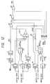
- Fig. 11 is a block diagram of a decoder section of a digital audio interface in a digital VTR.
- Fig. 12 is a block diagram of a circuit for generating a control signal AUDL.
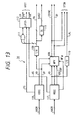
- Fig. 13 is a block diagram of the decoder of Fig. 4.
- Fig. 14 is a timing diagram showing the waveforms of various signals in the decoder of Fig. 13 which occur during a head of an odd field in a video field sequence.
- Fig. 15 is a timing diagram showing the waveforms of the signals in the decoder of Fig. 13 which occur during a head of an even field in the video field sequence.
- Fig. 16 is a block diagram of the video recording processing circuit of Fig. 2.
- a clock signal having a frequency "64fas” is used in the conversion of output serial data from a digital audio interface into 16-bit audio data.
- the clock signal having a frequency "64fas” is reproduced from a preamble of one sub frame by a clock reproducing circuit using a PLL (a phase-locked loop).
- An audio-data sampling clock signal having a frequency fas can be easily obtained by detecting the phase of the serial data, and by frequency-dividing the clock signal of a frequency "64fas” in synchronism with the detected phase.
- recorded audio information is automatically synchronized with recorded video information.
- audio information outputted from a digital audio equipment is recorded by a digital VTR, it is necessary to provide synchronization between the reproducing operation of the digital audio equipment and the recording operation of the digital VTR.
- a first prior art way of such synchronization has a step of feeding a reference video signal to both a digital audio equipment and a digital VTR.
- the speed of reproduction of audio information is controlled in response to the horizontal sync components of the reference video signal so that the previously-mentioned frequency relation (1) or (2) will be satisfied.
- the timing of recording of the audio information is controlled so as to correspond to the timing of recording of the reference video signal.
- Such a problem can be resolved by providing a digital audio equipment with a function of obtaining synchronization with a video signal.
- providing a digital audio equipment with a synchronizing function necessitates a large additional circuit.
- a fourth prior art way of synchronization has the step of generating a horizontal-frequency signal of reference video information on the basis of an audio sampling clock signal according to the previously-mentioned frequency relation (1) or (2).
- the horizontal-frequency signal is used as a reference for the recording operation of a digital VTR.
- the sampling frequency fs (13.5 MHz) related to component video data has the following relation with the horizontal frequency fh of NTSC and PALM television signals.
- fs 858fh
- the sampling frequency fs related to component video data has the following relation with the horizontal frequency fh of PAL television signals.
- fs 864fh
- a sampling clock signal used in the conversion of an analog video signal into digital video data is generated from a suitable-frequency signal, such as a composite sync signal, which has a frequency equal to a horizontal frequency fh.
- the positions of recording of digital data on a tape, the positions of the boundaries between audio data and video data on the tape, and the timing of recording of the digital data are determined by a video reference synchronous with a video sampling clock signal.
- composite-type digital VTRs require the generation of a signal of a video sampling frequency fsc which is related to an audio sampling frequency fas by the previously-mentioned equations (1), (2), (5), and (6). Accordingly, a large circuit tends to be necessary for synchronizing the recording operation of the digital VTR with the audio sampling clock signal.
- Fig. 11 shows a decoder section of a digital audio interface in a digital VTR.
- Fig. 1 shows the waveform of signals outputted from the decoder section of Fig. 11.
- the decoder section includes a clock reproducing circuit 100, serial decoders 101 and 102, serial-to-parallel (S/P) converters 103 and 104, and a multiplexer 105.
- the first serial data CH1/CH2 DATA and the second serial data CH3/CH4 DATA are synchronous with each other, and the clock reproducing circuit 100 generates the clock signal CLOCK on the basis of one of the first serial data CH1/CH2 DATA and the second serial data CH3/CH4 DATA.
- the present serial data is preferentially used in generating the clock signal CLOCK.
- the clock reproducing circuit 100 generates a sync signal ASYNC in response to the first serial data CH1/CH2 DATA and the second serial data CH3/CH4 DATA.
- a complete digital audio output signal from the digital VTR has a parallel form including 8 bits for audio information data, 1 bit for a 48-KHz sync signal ASYNC, and 1 bit for a 768-KHz clock signal CLOCK.
- the 8-bit audio information data, the 48-KHz sync signal ASYNC, and the 768-KHz clock signal CLOCK are in a fixed timing relation with each other.
- Each 16-bit audio data corresponding to a sample is divided into a byte "0" and a byte "1" before being transmitted.
- a byte "3" and a byte "4" are allotted to data for bit-number expansion, mode designation, and other purposes. Discrimination between channels is performed by referring to the 48-KHz sync signal ASYNC.
- video and audio data recording and reproducing apparatus includes a video recording processing circuit 1, an audio recording processing circuit 2, a multiplexer 3, a recording head 4, a magnetic tape 5, a reproducing head 6, a video reproducing processing circuit 7, an audio reproducing processing circuit 8, a burst lock oscillator 9, a video reference generating circuit 10, a servo circuit 11, a frequency converting circuit 12, and switches 13, 14, 15, and 16.
- a signal REF1 is a composite video signal which constitutes an output reference of a reproduced video signal, and which is inputted from an external signal source via a terminal (no reference character).
- the reference video signal REF1 contains sync and burst signals.
- the reference video signal REF1 is equal to or higher in level than a black burst in which all video information corresponds to a black level.
- the reference video signal REF1 is selected by the switch 15 as a reference video signal REF2 which is fed to the video reference generating circuit 10.
- the video reference generating circuit 10 detects horizontal and vertical sync signals, and a color framing phase and a subcarrier phase in a burst signal from the reference video signal REF2, and outputs signals of reproduction reference timings to the servo circuit 11, the audio reproducing processing circuit 8, and the video reproducing processing circuit 7.
- the video reference generating circuit 10 also outputs a black burst signal B.B. which is remade from a timing of the reference video signal REF2, and which includes sync and burst components having phases synchronous with the reference video signal REF2.
- Audio data (audio-information data) ADATA to be recorded is inputted from a digital audio interface (not shown) via a terminal (no reference character).
- Video data (video-information data) VDATA is inputted via another terminal (no reference character).
- the video data VDATA is fed from a video digital interface, or is obtained by the analog-to-digital conversion of a recording video signal which includes a process of sampling the recording video signal with a predetermined sampling clock signal.
- the audio recording processing circuit 2 receives the input audio data ADATA, which has four channels and which is transmitted while being separated into eight bits.
- the audio recording processing circuit 2 separates the input audio data ADATA into data of a channel "1", data of a channel "2", data of a channel "3", and data of a channel "4".
- the audio recording processing circuit 2 encodes the data of each channel into codes of a predetermined format, such as error-correcting codes, and outputs the audio-data codes to the multiplexer 3.
- the audio-data codes are fed to the recording head 4 via the multiplexer 3, being recorded on the magnetic tape 5 by the recording head 4.
- the recorded positions of the audio-data codes on the magnetic tape 5 are separated from the recorded positions of video data on the magnetic tape 5 by the operation of the multiplexer 3.
- a servo-control reference for a normal recording process is generated on the basis of the recording video data VDATA.
- the video recording processing circuit 1 receives the input video data VDATA via the switch, and converts the input video data VDATA into codes of a predetermined format similarly to the encoding of the audio data ADATA. In addition, the video recording processing circuit 1 generates a recording servo reference timing signal SVIN on the basis of the input video data VDATA, and feeds the reference signal SVIN to the servo circuit 11 via the switch 16.
- the switch 16 allows the transmission of the reference signal SVIN from the video recording processing circuit 1 to the servo circuit 11, and the switch 13 selects the externally-fed video data VDATA as recording video data RECDATA fed to the video recording processing circuit 1.
- the reference video signal REF2 transmitted via the switch 15 is also fed to the burst lock oscillator 9.
- the burst lock oscillator 9 generates a clock signal 4FSC1 on the basis of the burst signal in the reference video signal REF2.
- the clock signal 4FSC1 has a frequency equal to four times a color subcarrier frequency, and is phase-locked to the burst signal.
- the output clock signal 4FSC1 is selected by the switch 14 as a clock signal 4FSC fed to the video reference generating circuit 10.
- the video reference generating circuit 10 remakes a signal representative of a reference video reproduction timing in response to the clock signal 4FSC and the reference video signal REF2, and generates the black burst signal B.B.
- the video reference generating circuit 10 feeds a timing start pulse signal VRST for video output and a video processing clock signal 4FSC to the video reproducing processing circuit 7. Furthermore, the video reference generating circuit 10 feeds a timing start pulse signal ARST for audio output and an audio processing clock signal ARCK to the audio reproducing processing circuit 8.
- the video timing start pulse signal VRST, the audio timing start signal ARST, the video processing clock signal 4FSC, and the audio processing clock signal ARCK are synchronous with the black burst signal B.B.
- an editing process in this embodiment is different from that in the prior art recording and reproducing apparatus.
- the editing process is equal to a process of inserting new video information into recorded video information on a magnetic tape, or a process of re-recording a part of recorded information on the magnetic tape.
- recording video signal data VDATA or a reference video signal REF1 is used as a reference in such an editing process.
- This embodiment has a new mode of operation which is not taught by the prior art. During the new mode of operation, a recording timing is controlled in response to an input sync signal or an input clock signal from a digital audio interface.
- the switches 13, 14, and 15 are changed by a control signal AUDL.
- the switch 14 is changed so as to feed an output clock signal 4FSC2 from the frequency converting circuit 12 to the video reference generating circuit 10 as a clock signal 4FSC.
- the frequency converting circuit 12 receives sync components ASYNC of the input audio data ADATA from the digital audio interface, and generates the clock signal 4FSC2 on the basis of the sync components ASYNC of the audio data ADATA.
- the clock signal 4FSC2 has a frequency equal to four times the color subcarrier frequency fsc.
- the relation between the color subcarrier frequency fsc and the horizontal frequency fh is given by the previously-mentioned equation (5).
- the relation between the color subcarrier frequency fsc and the horizontal frequency fh is given by the previously-mentioned equation (6).
- the sync components ASYNC have a frequency equal to the audio signal sampling frequency fas, that is, 48 KHz.
- the relation between the frequency 4fsc of the clock signal 4FSC2 and the audio signal sampling frequency fas is given as follows.
- the frequency converting circuit 12 includes a combination of a frequency divider and a frequency multiplier cooperating to provide a frequency ratio in the equation (7) or (8).
- the frequency multiplier includes a PLL (phase-locked loop).
- the clock signal 4FSC2 may be generated by converting the frequency of a clock signal fed from a digital audio interface.
- the equations (7), (8), and (9) give the relation between the frequency fack of the digital-interface clock signal and the frequency 4fsc of the clock signal 4FSC2 in the NTSC system or the PAL system. This frequency ratio is used in the frequency converting circuit 12.
- the frequency converting circuit 12 compares the frequency of the first pulse signal and the frequency of the second pulse signal, and controls the frequency of the output clock signal 4FSC2 in response to the result of the frequency comparison so that the frequency of the first pulse signal will be locked to the frequency of the second pulse signal.
- the switch 13 is changed together with the switch 14. Specifically, the switch 13 is changed so as to feed timing data B.B.DATA from the video reference generating circuit 10 to the video recording processing circuit 1 instead of the recording video data VDATA.
- the timing data B.B.DATA is a base for the black burst signal B.B.
- the switch 13 may be changed so that the black burst signal B.B. will be fed instead of the analog video signal.
- the switch 15 is changed together with the switch 13.
- the switch 15 is opened so that the feed of the reference video signal REF2 to the video reference generating circuit 10 will be interrupted.
- the operation of the video reference generating circuit 10 moves into an internal mode or a self-running mode where a continuous video reference timing signal is internally and automatically generated.
- Fig. 12 shows a circuit for generating the control signal AUDL.
- sync signal separating circuits 70 and 74 serve to separate sync signals from the reference signal REF1 and the analog video signal respectively.
- Detection circuits 71 and 75 following the sync signal separating circuits 70 and 74 serve to detect the presence and absence of the separated sync signals. Specifically, the detection circuits 71 and 75 output "H" when video signals having normal sync signals are inputted. Otherwise, the detection circuits 71 and 75 output "L”.
- An analog-to-digital (A/D) converter 73 converts the analog input recording video signal into a corresponding digital signal.
- the selector 79 serves to select one of the digital input video signal and the analog input video signal.
- a selector 80 serves to select one of the externally-applied digital audio signal and the output digital audio signal from the P/S converter 78 as recording audio data ADATA. In other words, the selector 80 serves to select one of the digital input audio signal and the analog input audio signal.
- a gate 81 executes a predetermined logic operation among the output signals from the detection circuits 72 and 75 and a signal VSEL, and thereby outputs a signal VDET.
- the signal VSEL is fed from a system controller SYSCON (not shown) which provides an interface in the operation of the digital VTR.
- a gate 82 executes a predetermined logic operation between the output signal from the detection circuit 76 and a signal ASEL.
- the signal ASEL is fed from the system controller SYSCON.
- a gate 83 executes a predetermined logic operation between the output signals from the detection circuit 71 and the gate 81.
- the gate 84 executes a predetermined logic operation among the output signals from the gates 82 and 83 and a signal REC.
- the signal REC is fed from the system controller SYSCON.
- a gate 85 executes a predetermined logic operation between the output signal from the gate 84 and a signal AREF, and thereby outputs the control signal AUDL.
- the signal AREF is fed from the system controller SYSCON.
- the data selections by the selectors 79 and 80 are controlled in response to the signals VSEL and ASEL respectively. Specifically, the digital input signals are selected by the selectors 79 and 80 when the signals VSEL and ASEL are "H". Video data and audio data having a plurality of channels can be recorded. Simultaneously recording analog channels and digital channels can be done. For simplicity, a further description will be given of the case of one channel.
- the detection circuit 71 outputs a signal RDET which represents the presence and absence of the reference signal REF1.
- the gate 81 outputs a signal VDET which represents the presence and absence of an input video signal. specifically, the signal VDET assumes "H" in the presence of an input video signal. Otherwise, the signal VDET assumes "L".
- the gate 82 outputs a signal DADET.
- the signal DADET assumes "H” in the case where data from a digital interface is selected as recorded audio data and also the input signal is present. Otherwise, the signal DADET assumes "L". In the case of recording data of a plurality of channels, the signal DADET assumes "H” when at least one channel satisfies the above-mentioned conditions, and the signal DADET assumes "L” otherwise.
- the signal REC remains “H” during the recording process.
- the signal AREF is "H” when data from a digital interface is preferentially used as a reference for the record and reproduction.
- the black burst signal B.B. for a video output reference is generated from the clock signal 4FSC.
- the horizontal period given by the signal FH corresponds to 910 clock pulses as shown in Fig. 3, and the frequency of the burst signal is equal to one fourth of the clock signal.
- the switch 14 is changed by the control signal AUDL so that the output clock signal 4FSC2 from the frequency converting circuit 12 will be selected as the clock signal 4FSC fed to the video reference generating circuit 10.
- the black burst signal B.B. is continuously generated from the clock signal 4FSC.
- the output timing data B.B.DATA from the vide reference generating circuit 10 is selected by the switch 13 as the recording video data RECDATA fed to the video recording processing circuit 1.
- an internal recording video reference is generated in synchronism with a fixed-timing component of the audio data from the digital audio interface, and the internal recording video reference is fed to the video recording processing circuit 1.
- the multiplexer 3 and the servo circuit 11 can be prevented from operating asynchronously with the audio data, and it is possible to prevent the recorded audio data from partially dropping out or being discontinuous.
- the frequency converter 20 converts the sync signal ASYNC into a horizontal pulse signal AFH having a frequency equal to the horizontal frequency fh.
- the frequency converter 20 uses a frequency conversion ratio of 375/1144 in the case of the NTSC television system.
- the horizontal pulse signal AFH is fed to the phase comparator 21.
- the phase comparator 21, the low pass filter 22, the voltage-controlled oscillator 23, the switch 14, and a part of the video reference generating circuit 10 compose a PLL circuit 24.
- the output signal from the phase comparator 21 is fed to the voltage-controlled oscillator 23 via the low pass filter 22.
- the voltage-controlled oscillator 21 generates the clock signal 4FSC2 in response to the output signal from the phase comparator 21, and outputs the clock signal 4FSC2 to the video reference generating circuit 10 via the switch 14.
- the clock signal 4FSC2 is converted into a pulse signal FH through a frequency dividing process, the pulse signal FH having a frequency corresponding to the horizontal frequency fh.
- the pulse signal FH is outputted to the phase comparator 21.
- the phase of the pulse signal AFH and the phase of the pulse signal FH are compared by the phase comparator 21 so that the frequency of the clock signal 4FSC2 will have a fixed relation with the frequency of the sync component ASYNC of the input audio data.
- the subcarrier generating circuit 31 In the video reference generating circuit 10, the subcarrier generating circuit 31 generates a subcarrier FSC in response to the clock signal 4FSC fed via the switch 14.
- the horizontal counter 32 generates horizontal phase information data HADR in response to the clock signal 4FSC.
- the vertical counter 33 generates vertical phase information data VADR in response to the clock signal 4FSC.
- the subcarrier FSC, the horizontal phase information data HADR, and the vertical phase information data VADR constitute basic video references.
- the decoder 34 generates the horizontal pulse signal FH, timing data VTIM, a servo-control timing signal SVREF, a video reproducing reset pulse signal VRST, a field number signal FN, a composite sync signal CSYNC, and a burst flag signal BF on the basis of the horizontal phase information data HADR and the vertical phase information data VADR.
- the field number signal FN represents video phase information for matching the audio reproduction phase to the video reproduction phase.
- the burst gate 35 gates the subcarrier FSC in response to the burst flag signal BF, generating a burst signal from the subcarrier FSC and outputting the burst signal to the adder 36.
- the adder 36 combines the burst signal and the composite sync signal CSYNC into the black burst signal B.B. which is a video reference signal fed to an external equipment (not shown).
- the black burst signal B.B. has a waveform such as shown in Fig. 3.
- the reset pulse generating circuit 30 detects desired timings of resetting the subcarrier generating circuit 31, the horizontal counter 32, and the vertical counter 33 by referring to the reference video signal REF2, and generates reset timing signals representative thereof.
- the reference video signal REF2 is absent and the reset pulse generating circuit 30 does not output any reset timing signals.
- the subcarrier generating circuit 31 and the counters 32 and 33 move into a self-running mode of operation where suitable reset signals are internally generated.
- the frequency converter 38 converts the horizontal pulse signal FH into the digital-audio reproduced clock signal ARCK.
- the frequency converter 38 uses a frequency conversion ratio of 1144/375 in the case of the NTSC television system.
- the gate 37 gates the clock signal ARCK in response to the field number signal FN, generating the reset pulse signal ARST from the clock signal ARCK.
- the reset pulse signal ARST determines the digital audio reproduction phase.
- the digital data generating circuit 39 generates the recording video data B.B.DATA on the basis of the clock signal 4FSC and the timing data VTIM fed from the decoder 34.
- the contents of the recording video data B.B.DATA are equal to the contents of data obtained by the analog-to-digital conversion of the black burst signal B.B. which is executed at a sampling frequency equal to the frequency 4fsc.
- the recording video data B.B.DATA is used as a recording reference in a process of recording audio data during, for example, the after-recording of the audio data.
- the video data B.B.DATA is recorded as a reproduction reference for stably reproducing audio data.
- the decoder 34 includes a vertical address decoder 106, a horizontal address decoder 107, a multiplexer 108, frequency dividers 109 and 110, a NAND gate 111, a latch circuit 112, and a delay circuit 113.
- Fig. 14 shows the waveforms of various signals in the decoder 34 which occur during a head of an odd field in a video field sequence.
- Fig. 15 shows the waveforms of the signals in the decoder 34 which occur during a head of an even field in the video field sequence.
- the multiplexer 108 selects the pulse signal VSP. During the absence of a pulse of the signal VP and the presence of a pulse of the signal VD, the multiplexer 108 selects the equalizing pulse signal EQP. These processes by the multiplexer 108 causes the generation of the composite sync signal CSYNC of Figs. 14 and 15. In addition, the multiplexer 108 inhibits or blocks the pulse signal BFO in response to the pulse signal VD at a burst position in a horizontal period, and thereby generates the burst flag signal BF which is fed to the burst gate 35 of Fig. 4.
- the delay circuit 113 generates the reproduction reference timing signal SVREF by suitably delaying the output signal from the frequency divider 109.
- the speed of a drum provided with a rotary head is controlled in synchronism with a video field, and the reproduction timing is controlled by suitably setting the phase of the field number signal FN.
- the pulse signals CSYNC, BF, and LAL compose the timing data VTIM which is used by the digital data generating circuit 39 of Fig. 4 in generating the black burst data B.B.DATA.
- the digital data generating circuit 39 includes a counter and a ROM storing inclination data.
- the counter serves to detect an interval of several clocks in response to variation points of the pulse signals CSYNC and BF, and the inclination data is read out from the ROM by using the output signal from the counter as an address fed to the ROM. As a result of this process, burst envelope data and composite sync data having an inclination are obtained.
- the black burst data B.B.DATA can be obtained by multiplying the burst envelope data and color subcarrier data to generate burst data, and by adding the burst data and the composite sync data.
- the color subcarrier data agrees with data representing sinusoidal waves having a period equal to the color subcarrier period.
- the generation of the black burst data B.B.DATA is shown, for example, in U.S. Application Serial Number 789,069, U.S. Application Serial Number 853,304, or Japanese published unexamined patent application 62-18586, the disclosure of which is hereby incorporated by reference.
- the pulse signal LAL is used in determining the phase relation between the composite sync data and the color subcarrier data.
- the time portions of the black burst data B.B.DATA except the sync and burst parts agree with blanking level data, and thus they can be generated easily.
- the digital data generating circuit 39 for generating the black burst data B.B.DATA representing a video signal containing burst components may be omitted, and be replaced by another simple circuit.
- This circuit in the video reference generating circuit 10 is used in common for the PLL circuit 24, and thus it is unnecessary to provide the frequency converting circuit 12 with a circuit for generating a horizontal pulse signal FH from the clock signal 4FSC2. Accordingly, the combination of the frequency converting circuit 12 and the video reference generating circuit 10 can be made on a small scale.
- the frequency converter 20 can be used in common for generating a reference signal of a horizontal frequency fh from a clock signal of a sampling frequency fas, the reference horizontal frequency signal being compared in phase to the horizontal pulse signal FH in a PLL for generating the sampling clock signal from the horizontal pulse signal FH, the sampling clock signal being used in the analog-to-digital conversion of an analog audio signal.
- a second embodiment of this invention is similar to the embodiment of Figs. 2-6 except for design changes indicated later.
- the second embodiment is designed for a PAL video signal.
- the horizontal pulse signal FH2 is fed to the phase comparator 21 within the frequency converting circuit 12.
- the decoder 34b generates timing data VTIMb, a field number signal FN, a composite sync signal CSYNC, and a burst flag signal BF on the basis of horizontal phase information data HADRb and vertical phase information data VADR fed from the horizontal counter 32b and the vertical counter 33.
- the timing data VTIMb constitutes a base for generating video signal data.
- the timing data VTIMb is fed to the decoder 34a.
- the field number signal FN represents video phase information for matching the audio reproduction phase to the video reproduction phase.
- the decoder 34a generates timing data VTIM on the basis of the timing data VTIMb and the horizontal phase information data HADRa.
- the output video data B.B.DATA from the ROM 52 is denoted by sampling-point circles which are positioned at corresponding analog levels for an easy understanding.
- the video data B.B.DATA has a given timing relation with the subcarrier phase data SCP as shown in Fig. 10.
- the horizontal frequency fh and the sampling clock frequency 4fsc have the offset relation expressed in the previously-mentioned equation (10). Therefore, as shown in Fig. 10, the waveform sampling points of the video data B.B.DATA gradually shift relative to the phase of the horizontal sync signal in each horizontal period. The rate of this shift corresponds to the period of the clock signal 4FSC which is multiplied by 4/625.
- the video data B.B.DATA is converted by the combination of the D/A converter 54 and the low pass filter 55 into the continuous-waveform black burst signal B.B. which has a constant horizontal period (see Fig. 10).
- the horizontal pulse signal FH outputted from the horizontal sync separating circuit 56 is free from an offset process, and has a fixed frequency relation with the clock signal 4FSC.
Description
- This invention relates to a video and audio data apparatus usable in combination with a digital audio interface, in particular to a digital VTR (video tape recorder), which can record, reproduce, and edit video data and audio data.
- In the field of digital audio, there are standards for digital audio interfaces connecting digital audio equipments as disclosed in AES-1985 (ANSI S4.40-1985). Some of industrial-use and broadcast-use VTRs are of the digital type executing digital recording of a video signal. Known apparatus can simultaneously record, reproduce, and edit digital video data and digital audio data, the digital video data being derived from a video signal, the digital audio data being outputted from a digital audio interface. As will be explained later, such prior art recording and reproducing apparatus have some problems.
- The document GB-A-2 166 278 relates to a sound recording interface for a domestic video cassette recorder which creates a standard television signal on a spare UHF channel of a "black" picture and the desired sound. This signal can be recorded and played back by the video cassette recorder like a normal television signal and therefore, radio programmes as well as any mix of radio and television programmes can be recorded on a video cassette recorder.
- US-patent US-A-4,816,926 relates to an information signal recording apparatus which can be used also as an audio tape recorder only. When using this apparatus only as an audio tape recorder, the audio signal is sampled with a frequency m times the sampling frequency of an audio signal which is used upon recording a video signal and the thus sampled PCM digital audio signal is diffusively recorded on at least two recording intervals thereby to improve the tone quality of the audio signal. Thus, the compatibility with the audio tape recorder using a video tape recorder of the same kind can be established.
- The document EP-A-0 206 752 discloses an apparatus for recording and reproducing a video signal and an audio signal which are recorded in different areas or portions of a tape. The apparatus includes a circuit for supplying a new audio signal from an input terminal to the rotary heads for recording, a signal generator for generating a pre-determined signal to be substituted for the processed luminance component, and a muting circuit for muting the reproduced chrominance component. The predetermined signal from the signal generator is substituted for the processed luminance component, and the chrominance component is muted by the muting circuit during recording of the audio signal in place of a previously recorded audio signal, thereby suppressing noise bars which might otherwise appear in the reproduced picture.
- In the document "8th International Conference on Video, Audio and Data Recording (Proceedings), April 1990, Birmingham, pages 93 to 100" a recorder for baseband HDTV is disclosed. This paper reports on the details of video and audio signal processing methods and system constitution of a 1/2-inch cassette HDVTR. In particular, a method is reported to overcome the problems resulted from the thin tape and small diameter drum with high rotating speed for recording the HDTV signal as well as a high speed velocity error compensation method.
- Document EP-A-0 366 402 relates to a method of recording/reproducing a digital audio signal together with a video signal. The digital audio signal matchable with standard digital audio interface is divided by a field period of the video signal to constitute processing units. A block completed interleave is performed on the data of each processing unit in a three dimensional space including (18x18x5) samples in the NTSC system or (18x18x6) samples in the case of the CCIR system. First and second error correction codes are generated orthogonally to the (18x18) playing of the three dimensional space and added to the digital audio data.
- The object of the invention is to provide an improved video and audio data recording apparatus.
- This object is achieved by a video and audio data recording apparatus according to
claim 1. - Fig. 1 is a timing diagram showing the waveforms of components of an output signal from a digital audio interface.
- Fig. 2 is a block diagram of a video and audio data recording and reproducing apparatus according to a first embodiment of this invention.
- Fig. 3 is a timing diagram showing the waveforms of signals in the apparatus of Fig. 2.
- Fig. 4 is a block diagram showing the details of the frequency converting circuit and the video reference generating circuit of Fig. 2.
- Fig. 5 is a timing diagram showing the waveforms of signals in the frequency converting circuit of Fig. 4.
- Fig. 6 is a timing diagram showing the waveforms of signals in the frequency converting circuit of Fig. 4.
- Fig. 7 is a block diagram of a part of a video and audio data recording and reproducing apparatus according to a second embodiment of this invention.
- Fig. 8 is a timing diagram showing the waveforms of signals in the apparatus of Fig. 7.
- Fig. 9 is a block diagram of a part of a video and audio data recording and reproducing apparatus according to a third embodiment of this invention.
- Fig. 10 is a timing diagram showing the waveforms of signals in the apparatus of Fig. 9.
- Fig. 11 is a block diagram of a decoder section of a digital audio interface in a digital VTR.
- Fig. 12 is a block diagram of a circuit for generating a control signal AUDL.
- Fig. 13 is a block diagram of the decoder of Fig. 4.
- Fig. 14 is a timing diagram showing the waveforms of various signals in the decoder of Fig. 13 which occur during a head of an odd field in a video field sequence.
- Fig. 15 is a timing diagram showing the waveforms of the signals in the decoder of Fig. 13 which occur during a head of an even field in the video field sequence.
- Fig. 16 is a block diagram of the video recording processing circuit of Fig. 2.
- Fig. 17 is a block diagram showing a modification of the embodiment of Figs. 2 and 16.
- In general digital audio interfaces, a signal of one system can transmit data of two channels, and data corresponding to a sample is transmitted as 32-bit serial data. In general digital VTRs, audio data results from a 16-bit linear quantization using a sampling frequency fas of 48 KHz, and parallel data corresponding to a sample is converted into serial data. The serial data corresponding to a sample, a preamble, expansion data bits, and error detection or error correction bits are combined into one sub frame of serial data. In the digital audio interfaces, since data of two channels are multiplexed in a time division manner before being transmitted, the bit transmission rate corresponds to 64 bits per sample of audio data and the frequency of a clock signal for data transmission is equal to 64 times the frequency fas. A clock signal having a frequency "64fas" is used in the conversion of output serial data from a digital audio interface into 16-bit audio data. The clock signal having a frequency "64fas" is reproduced from a preamble of one sub frame by a clock reproducing circuit using a PLL (a phase-locked loop). An audio-data sampling clock signal having a frequency fas can be easily obtained by detecting the phase of the serial data, and by frequency-dividing the clock signal of a frequency "64fas" in synchronism with the detected phase.
- During the transfer of information between tapes in digital VTRs, a reproduced video signal outputted from a first VTR determines the speed of recording of the information into the tape of a second VTR, and an audio signal is outputted from the first VTR at a phase fixed relative to the phase of the output video signal.
- In the NTSC and PALM television systems, the relation of the sampling frequency fas for audio information with the horizontal frequency fh of a video signal is expressed by the following equation.

- In the PAL television systems, the relation of the sampling frequency fas for audio information with the horizontal frequency fh of a video signal is expressed by the following equation.

- During the dubbing of audio and video information between tapes of digital VTRs, recorded audio information is automatically synchronized with recorded video information. In the case where audio information outputted from a digital audio equipment is recorded by a digital VTR, it is necessary to provide synchronization between the reproducing operation of the digital audio equipment and the recording operation of the digital VTR.
- A first prior art way of such synchronization has a step of feeding a reference video signal to both a digital audio equipment and a digital VTR. In the digital audio equipment, the speed of reproduction of audio information is controlled in response to the horizontal sync components of the reference video signal so that the previously-mentioned frequency relation (1) or (2) will be satisfied. In the digital VTR, the timing of recording of the audio information is controlled so as to correspond to the timing of recording of the reference video signal.
- A second prior art way of synchronization is realized by a synchronizing interface between a digital audio equipment and a digital VTR. The digital audio equipment is designed so as to have the additional function of generating a sync signal such as a composite sync signal which is synchronous with a sampling clock signal for reproduced data. The synchronizing interface transmits the sync signal from the digital audio equipment to the digital VTR. In the digital VTR, the timing of recording of the audio information is controlled in response to the sync signal.
- According to a third prior art way of synchronization, a digital VTR is designed so as to have the additional function of generating a sampling clock signal synchronous with an information recording timing. The sampling clock signal is transmitted to a digital audio equipment. In the digital audio equipment, the timing of reproduction of audio information is controlled in response to the sampling clock signal.
- Most of home-use digital audio equipments such as home-use digital audio tape recorders can not accept a reference video signal and a composite sync signal. Thus, the reproducing operation of these home-use digital audio equipments can not be synchronized with the recording operation of a digital VTR. In the absence of synchronization between the reproducing operation of a digital audio equipment and the recording operation of a digital VTR, the quality of recorded and reproduced audio information tends to be deteriorated.
- Such a problem can be resolved by providing a digital audio equipment with a function of obtaining synchronization with a video signal. In general, providing a digital audio equipment with a synchronizing function necessitates a large additional circuit. In addition, it is necessary to provide a source for generating a reference video signal.
- A fourth prior art way of synchronization has the step of generating a horizontal-frequency signal of reference video information on the basis of an audio sampling clock signal according to the previously-mentioned frequency relation (1) or (2). The horizontal-frequency signal is used as a reference for the recording operation of a digital VTR.
- In 4:2:2 component-type digital VTRs (D-1 format) according to standards of CCIR REC. 657, the sampling frequency fs (13.5 MHz) related to component video data has the following relation with the horizontal frequency fh of NTSC and PALM television signals.


- Edwin Engberg et al published "The Composite Digital Format and its Applications", SMPTE Television Conference. San Francisco, February 1987. This publication relates to composite-type digital VTRs (D-2 format) in which a television signal is sampled at a frequency equal to a multiple of a color subcarrier frequency, and a composite video signal is subjected to a digital recording process. It is generally difficult to synchronize the recording operation of such a digital VTR with audio data.
- For example. in a digital VTR of the D-2 format, a video sampling frequency fs is equal to four times a color subcarrier frequency fsc. The video sampling frequency fs has a simple relation with the horizontal frequency fh of an NTSC television signal since there is the following simple ratio between the horizontal frequency fh and the color subcarrier frequency fsc of the NTSC television signal.


- In digital VTRs, the positions of recording of digital data on a tape, the positions of the boundaries between audio data and video data on the tape, and the timing of recording of the digital data are determined by a video reference synchronous with a video sampling clock signal. Thus, composite-type digital VTRs require the generation of a signal of a video sampling frequency fsc which is related to an audio sampling frequency fas by the previously-mentioned equations (1), (2), (5), and (6). Accordingly, a large circuit tends to be necessary for synchronizing the recording operation of the digital VTR with the audio sampling clock signal.
- Fig. 11 shows a decoder section of a digital audio interface in a digital VTR. Fig. 1 shows the waveform of signals outputted from the decoder section of Fig. 11.
- As shown in Fig. 11, the decoder section includes a
clock reproducing circuit 100,serial decoders 101 and 102, serial-to-parallel (S/P)converters multiplexer 105. - Since a normal digital VRT can record audio data of four channels, the decoder section of Fig. 11 is designed so as to handle first serial data CH1/CH2 DATA and second serial data CH3/CH4 DATA which compose four channels. The
serial decoders 101 and 102 receive the first serial data CH1/CH2 DATA and the second serial data CH3/CH4 DATA respectively, and extracts necessary data portions therefrom. Theclock reproducing circuit 100 receives the first serial data CH1/CH2 DATA and the second serial data CH3/CH4 DATA, and reproduces a clock signal CLOCK of a frequency "64fas" from the preamble of the received data. The first serial data CH1/CH2 DATA and the second serial data CH3/CH4 DATA are synchronous with each other, and theclock reproducing circuit 100 generates the clock signal CLOCK on the basis of one of the first serial data CH1/CH2 DATA and the second serial data CH3/CH4 DATA. In the case where one of the first serial data CH1/CH2 DATA and the second serial data CH3/CH4 DATA is present but the other is absent, the present serial data is preferentially used in generating the clock signal CLOCK. In addition, theclock reproducing circuit 100 generates a sync signal ASYNC in response to the first serial data CH1/CH2 DATA and the second serial data CH3/CH4 DATA. The output data from theserial decoders 101 and 102 are converted by the S/P converters P converter 103 and the output 8-bit parallel data from the S/P converter 104 are multiplexed by themultiplexer 105 in a time division manner. The output 8-bit parallel data from themultiplexer 105, the output clock signal CLOCK from theclock reproducing circuit 100, and the output sync signal ASYNC from theclock reproducing circuit 100 are transmitted to an external device. The output 8-bit parallel data from themultiplexer 105, the output clock signal CLOCK from theclock reproducing circuit 100, and the output sync signal ASYNC from theclock reproducing circuit 100 have a predetermined timing relation such as shown in Fig. 1. - The conversion into 8-bit data is adopted in view of the following facts. Processing 8-bit data is general, and a hardware for processing 8-bit data is usually simple. In a normal digital VTR, video data has an 8-bit parallel form. Thus, the conversion into 8-bit data enables a portion of the circuit to be used in common by a video processing circuit.
- As is understood from the previous description, a complete digital audio output signal from the digital VTR has a parallel form including 8 bits for audio information data, 1 bit for a 48-KHz sync signal ASYNC, and 1 bit for a 768-KHz clock signal CLOCK. As shown in Fig. 1, the 8-bit audio information data, the 48-KHz sync signal ASYNC, and the 768-KHz clock signal CLOCK are in a fixed timing relation with each other. Each 16-bit audio data corresponding to a sample is divided into a byte "0" and a byte "1" before being transmitted. A byte "3" and a byte "4" are allotted to data for bit-number expansion, mode designation, and other purposes. Discrimination between channels is performed by referring to the 48-KHz sync signal ASYNC.
- With reference to Fig. 2, video and audio data recording and reproducing apparatus includes a video
recording processing circuit 1, an audiorecording processing circuit 2, amultiplexer 3, arecording head 4, amagnetic tape 5, a reproducinghead 6, a video reproducing processing circuit 7, an audio reproducingprocessing circuit 8, aburst lock oscillator 9, a videoreference generating circuit 10, aservo circuit 11, afrequency converting circuit 12, and switches 13, 14, 15, and 16. - A signal REF1 is a composite video signal which constitutes an output reference of a reproduced video signal, and which is inputted from an external signal source via a terminal (no reference character). The reference video signal REF1 contains sync and burst signals. The reference video signal REF1 is equal to or higher in level than a black burst in which all video information corresponds to a black level. The reference video signal REF1 is selected by the
switch 15 as a reference video signal REF2 which is fed to the videoreference generating circuit 10. The videoreference generating circuit 10 detects horizontal and vertical sync signals, and a color framing phase and a subcarrier phase in a burst signal from the reference video signal REF2, and outputs signals of reproduction reference timings to theservo circuit 11, the audio reproducingprocessing circuit 8, and the video reproducing processing circuit 7. The videoreference generating circuit 10 also outputs a black burst signal B.B. which is remade from a timing of the reference video signal REF2, and which includes sync and burst components having phases synchronous with the reference video signal REF2. - Audio data (audio-information data) ADATA to be recorded is inputted from a digital audio interface (not shown) via a terminal (no reference character). Video data (video-information data) VDATA is inputted via another terminal (no reference character). The video data VDATA is fed from a video digital interface, or is obtained by the analog-to-digital conversion of a recording video signal which includes a process of sampling the recording video signal with a predetermined sampling clock signal. The audio
recording processing circuit 2 receives the input audio data ADATA, which has four channels and which is transmitted while being separated into eight bits. The audiorecording processing circuit 2 separates the input audio data ADATA into data of a channel "1", data of a channel "2", data of a channel "3", and data of a channel "4". Then, the audiorecording processing circuit 2 encodes the data of each channel into codes of a predetermined format, such as error-correcting codes, and outputs the audio-data codes to themultiplexer 3. The audio-data codes are fed to therecording head 4 via themultiplexer 3, being recorded on themagnetic tape 5 by therecording head 4. The recorded positions of the audio-data codes on themagnetic tape 5 are separated from the recorded positions of video data on themagnetic tape 5 by the operation of themultiplexer 3. As will be explained later, a servo-control reference for a normal recording process is generated on the basis of the recording video data VDATA. The videorecording processing circuit 1 receives the input video data VDATA via the switch, and converts the input video data VDATA into codes of a predetermined format similarly to the encoding of the audio data ADATA. In addition, the videorecording processing circuit 1 generates a recording servo reference timing signal SVIN on the basis of the input video data VDATA, and feeds the reference signal SVIN to theservo circuit 11 via theswitch 16. During the normal recording process, theswitch 16 allows the transmission of the reference signal SVIN from the videorecording processing circuit 1 to theservo circuit 11, and theswitch 13 selects the externally-fed video data VDATA as recording video data RECDATA fed to the videorecording processing circuit 1. - During a normal reproducing process, the video
reference generating circuit 10 feeds a reproduction reference timing signal SVREF to theservo circuit 11 via theswitch 16, and the reproducinghead 6 reproduces recorded data from thetape 5. The reproduced data outputted from the reproducinghead 6 is decoded by the video reproducing processing circuit 7 and the audio reproducingprocessing circuit 8 into reproduced video data VIDEO-OUT and reproduced audio data AUDIO-OUT which are outputted to an external device (not shown). - The reference video signal REF2 transmitted via the
switch 15 is also fed to theburst lock oscillator 9. Theburst lock oscillator 9 generates a clock signal 4FSC1 on the basis of the burst signal in the reference video signal REF2. The clock signal 4FSC1 has a frequency equal to four times a color subcarrier frequency, and is phase-locked to the burst signal. During the normal reproducing process, the output clock signal 4FSC1 is selected by theswitch 14 as a clock signal 4FSC fed to the videoreference generating circuit 10. Thus, the videoreference generating circuit 10 remakes a signal representative of a reference video reproduction timing in response to the clock signal 4FSC and the reference video signal REF2, and generates the black burst signal B.B. which can be used as a video reference for an external equipment (not shown). In addition, the videoreference generating circuit 10 feeds a timing start pulse signal VRST for video output and a video processing clock signal 4FSC to the video reproducing processing circuit 7. Furthermore, the videoreference generating circuit 10 feeds a timing start pulse signal ARST for audio output and an audio processing clock signal ARCK to the audio reproducingprocessing circuit 8. The video timing start pulse signal VRST, the audio timing start signal ARST, the video processing clock signal 4FSC, and the audio processing clock signal ARCK are synchronous with the black burst signal B.B. - While the normal recording process and the normal reproducing process in this embodiment are similar to those in a prior art recording and reproducing apparatus, an editing process in this embodiment is different from that in the prior art recording and reproducing apparatus. For example, the editing process is equal to a process of inserting new video information into recorded video information on a magnetic tape, or a process of re-recording a part of recorded information on the magnetic tape. It is known that recording video signal data VDATA or a reference video signal REF1 is used as a reference in such an editing process. This embodiment has a new mode of operation which is not taught by the prior art. During the new mode of operation, a recording timing is controlled in response to an input sync signal or an input clock signal from a digital audio interface.
- In the case where audio data ADATA is asynchronous with video data VDATA or a reference video signal REF1, and in the case where video data VDATA or a reference video signal REF1 is absent, the
switches switch 14 is changed so as to feed an output clock signal 4FSC2 from thefrequency converting circuit 12 to the videoreference generating circuit 10 as a clock signal 4FSC. Thefrequency converting circuit 12 receives sync components ASYNC of the input audio data ADATA from the digital audio interface, and generates the clock signal 4FSC2 on the basis of the sync components ASYNC of the audio data ADATA. The clock signal 4FSC2 has a frequency equal to four times the color subcarrier frequency fsc. In the NTSC television system, the relation between the color subcarrier frequency fsc and the horizontal frequency fh is given by the previously-mentioned equation (5). In the PAL television system, the relation between the color subcarrier frequency fsc and the horizontal frequency fh is given by the previously-mentioned equation (6). The sync components ASYNC have a frequency equal to the audio signal sampling frequency fas, that is, 48 KHz. Thus, in the NTSC television system, by referring to the previously-mentioned equations (1) and (5), the relation between the frequency 4fsc of the clock signal 4FSC2 and the audio signal sampling frequency fas is given as follows.

frequency converting circuit 12 includes a combination of a frequency divider and a frequency multiplier cooperating to provide a frequency ratio in the equation (7) or (8). For example, the frequency multiplier includes a PLL (phase-locked loop). - It should be noted that the clock signal 4FSC2 may be generated by converting the frequency of a clock signal fed from a digital audio interface. The clock signal of Fig. 1 which is fed from the digital audio interface has a frequency fack of 768 KHz, and the clock signal frequency fack is related with the audio signal sampling frequency fas as follows.

frequency converting circuit 12. - It should be noted that the frequency 4fsc of the clock signal 4FSC2 may be controlled as follows. The video
reference generating circuit 10 divides the frequency 4fsc of the input clock signal 4FSC2 with a factor corresponding to the frequency ratio in the previously-mentioned equation (5) or (6), and thereby generates a first pulse signal FH with a frequency corresponding to the horizontal frequency fh. The first pulse signal FH is outputted from the videoreference generating circuit 10 to thefrequency converting circuit 12. Thefrequency converting circuit 12 generates a second pulse signal on the basis of the sync signal ASYNC by referring to the frequency relation in the previously-mentioned equation (1) or (2), the second pulse signal having a frequency equal to the horizontal frequency fh. Thefrequency converting circuit 12 compares the frequency of the first pulse signal and the frequency of the second pulse signal, and controls the frequency of the output clock signal 4FSC2 in response to the result of the frequency comparison so that the frequency of the first pulse signal will be locked to the frequency of the second pulse signal. - In the case where the audio data ADATA is asynchronous with the video data VDATA or the reference video signal REF1, and in the case where the video data VDATA or the reference video signal REF1 is absent, the
switch 13 is changed together with theswitch 14. Specifically, theswitch 13 is changed so as to feed timing data B.B.DATA from the videoreference generating circuit 10 to the videorecording processing circuit 1 instead of the recording video data VDATA. The timing data B.B.DATA is a base for the black burst signal B.B. In the presence of a function of converting an analog video signal into a digital video signal and recording the digital video signal, theswitch 13 may be changed so that the black burst signal B.B. will be fed instead of the analog video signal. Theswitch 15 is changed together with theswitch 13. Specifically, theswitch 15 is opened so that the feed of the reference video signal REF2 to the videoreference generating circuit 10 will be interrupted. In this case, the operation of the videoreference generating circuit 10 moves into an internal mode or a self-running mode where a continuous video reference timing signal is internally and automatically generated. - A further description will be given with reference to Fig. 3. In Fig. 3, video data VDATA for a VTR recording reference is shown as a color burst signal. During the normal operation, the reference video signal REF1 is equal to the video data VDATA. Under conditions where the recording video data VDATA and the reference video signal REF1 are absent but audio data ADATA is inputted from a digital audio interface, when a recording process or an after-recording process is required to be done, a suitable device (not shown) detects the absence of the video data VDATA and the video signal REF1 and changes the logic level of the control signal AUDL from "H" to "L" in response thereto. This change of the control signal AUDL causes the
switches - Fig. 12 shows a circuit for generating the control signal AUDL. In Fig. 12, sync
signal separating circuits Detection circuits signal separating circuits detection circuits detection circuits converter 73 converts the analog input recording video signal into a corresponding digital signal. An analog-to-digital (A/D) converter 77 converts the analog input recording audio signal into a corresponding digital signal.Detection circuits detection circuits detection circuits D converter 73 as recording video data VDATA. In other words, the selector 79 serves to select one of the digital input video signal and the analog input video signal. Aselector 80 serves to select one of the externally-applied digital audio signal and the output digital audio signal from the P/S converter 78 as recording audio data ADATA. In other words, theselector 80 serves to select one of the digital input audio signal and the analog input audio signal. Agate 81 executes a predetermined logic operation among the output signals from thedetection circuits gate 82 executes a predetermined logic operation between the output signal from thedetection circuit 76 and a signal ASEL. The signal ASEL is fed from the system controller SYSCON. Agate 83 executes a predetermined logic operation between the output signals from thedetection circuit 71 and thegate 81. Thegate 84 executes a predetermined logic operation among the output signals from thegates gate 85 executes a predetermined logic operation between the output signal from thegate 84 and a signal AREF, and thereby outputs the control signal AUDL. The signal AREF is fed from the system controller SYSCON. - The data selections by the
selectors 79 and 80 are controlled in response to the signals VSEL and ASEL respectively. Specifically, the digital input signals are selected by theselectors 79 and 80 when the signals VSEL and ASEL are "H". Video data and audio data having a plurality of channels can be recorded. Simultaneously recording analog channels and digital channels can be done. For simplicity, a further description will be given of the case of one channel. Thedetection circuit 71 outputs a signal RDET which represents the presence and absence of the reference signal REF1. Thegate 81 outputs a signal VDET which represents the presence and absence of an input video signal. specifically, the signal VDET assumes "H" in the presence of an input video signal. Otherwise, the signal VDET assumes "L". Thegate 82 outputs a signal DADET. The signal DADET assumes "H" in the case where data from a digital interface is selected as recorded audio data and also the input signal is present. Otherwise, the signal DADET assumes "L". In the case of recording data of a plurality of channels, the signal DADET assumes "H" when at least one channel satisfies the above-mentioned conditions, and the signal DADET assumes "L" otherwise. The signal REC remains "H" during the recording process. The signal AREF is "H" when data from a digital interface is preferentially used as a reference for the record and reproduction. - In the video
reference generating circuit 10, the black burst signal B.B. for a video output reference is generated from the clock signal 4FSC. In the NTSC television system, the horizontal period given by the signal FH corresponds to 910 clock pulses as shown in Fig. 3, and the frequency of the burst signal is equal to one fourth of the clock signal. In the absence of the recording video signal data, theswitch 14 is changed by the control signal AUDL so that the output clock signal 4FSC2 from thefrequency converting circuit 12 will be selected as the clock signal 4FSC fed to the videoreference generating circuit 10. The black burst signal B.B. is continuously generated from the clock signal 4FSC. At the same time, the output timing data B.B.DATA from the videreference generating circuit 10 is selected by theswitch 13 as the recording video data RECDATA fed to the videorecording processing circuit 1. - According to this embodiment, even in the absence of an external recording video reference, an internal recording video reference is generated in synchronism with a fixed-timing component of the audio data from the digital audio interface, and the internal recording video reference is fed to the video
recording processing circuit 1. Thus, themultiplexer 3 and theservo circuit 11 can be prevented from operating asynchronously with the audio data, and it is possible to prevent the recorded audio data from partially dropping out or being discontinuous. - A detailed description will be given of the
frequency converting circuit 12 and the videoreference generating circuit 10 with reference to Fig. 4. As shown in Fig. 4, the videoreference generating circuit 10 includes a resetpulse generating circuit 30 for determining the phase of a video reference, asubcarrier generating circuit 31 for frequency-dividing the clock signal 4FSC to generate a color subcarrier, ahorizontal counter 32 for counting horizontal periods by referring to the clock signal 4FSC, avertical counter 33 for counting vertical periods, adecoder 34, aburst gate 35, anadder 36, agate 37, afrequency converter 38, and a digitaldata generating circuit 39 for generating the recording reference video data B.B.DATA. As shown in Fig. 4, thefrequency converting circuit 12 includes afrequency converter 20, aphase comparator 21, alow pass filter 22, and a voltage-controlledoscillator 23. - In the
frequency converting circuit 12, thefrequency converter 20 converts the sync signal ASYNC into a horizontal pulse signal AFH having a frequency equal to the horizontal frequency fh. Thefrequency converter 20 uses a frequency conversion ratio of 375/1144 in the case of the NTSC television system. The horizontal pulse signal AFH is fed to thephase comparator 21. Thephase comparator 21, thelow pass filter 22, the voltage-controlledoscillator 23, theswitch 14, and a part of the videoreference generating circuit 10 compose aPLL circuit 24. The output signal from thephase comparator 21 is fed to the voltage-controlledoscillator 23 via thelow pass filter 22. The voltage-controlledoscillator 21 generates the clock signal 4FSC2 in response to the output signal from thephase comparator 21, and outputs the clock signal 4FSC2 to the videoreference generating circuit 10 via theswitch 14. In the videoreference generating circuit 10, the clock signal 4FSC2 is converted into a pulse signal FH through a frequency dividing process, the pulse signal FH having a frequency corresponding to the horizontal frequency fh. The pulse signal FH is outputted to thephase comparator 21. The phase of the pulse signal AFH and the phase of the pulse signal FH are compared by thephase comparator 21 so that the frequency of the clock signal 4FSC2 will have a fixed relation with the frequency of the sync component ASYNC of the input audio data. - In the video
reference generating circuit 10, thesubcarrier generating circuit 31 generates a subcarrier FSC in response to the clock signal 4FSC fed via theswitch 14. Thehorizontal counter 32 generates horizontal phase information data HADR in response to the clock signal 4FSC. Thevertical counter 33 generates vertical phase information data VADR in response to the clock signal 4FSC. The subcarrier FSC, the horizontal phase information data HADR, and the vertical phase information data VADR constitute basic video references. Thedecoder 34 generates the horizontal pulse signal FH, timing data VTIM, a servo-control timing signal SVREF, a video reproducing reset pulse signal VRST, a field number signal FN, a composite sync signal CSYNC, and a burst flag signal BF on the basis of the horizontal phase information data HADR and the vertical phase information data VADR. The field number signal FN represents video phase information for matching the audio reproduction phase to the video reproduction phase. Theburst gate 35 gates the subcarrier FSC in response to the burst flag signal BF, generating a burst signal from the subcarrier FSC and outputting the burst signal to theadder 36. Theadder 36 combines the burst signal and the composite sync signal CSYNC into the black burst signal B.B. which is a video reference signal fed to an external equipment (not shown). The black burst signal B.B. has a waveform such as shown in Fig. 3. - In the video
reference generating circuit 10, the resetpulse generating circuit 30 detects desired timings of resetting thesubcarrier generating circuit 31, thehorizontal counter 32, and thevertical counter 33 by referring to the reference video signal REF2, and generates reset timing signals representative thereof. In the case where the recording is done by using the audio data ADATA as a reference, the reference video signal REF2 is absent and the resetpulse generating circuit 30 does not output any reset timing signals. In this case, thesubcarrier generating circuit 31 and thecounters frequency converter 38 converts the horizontal pulse signal FH into the digital-audio reproduced clock signal ARCK. Thefrequency converter 38 uses a frequency conversion ratio of 1144/375 in the case of the NTSC television system. Thegate 37 gates the clock signal ARCK in response to the field number signal FN, generating the reset pulse signal ARST from the clock signal ARCK. The reset pulse signal ARST determines the digital audio reproduction phase. The digitaldata generating circuit 39 generates the recording video data B.B.DATA on the basis of the clock signal 4FSC and the timing data VTIM fed from thedecoder 34. The contents of the recording video data B.B.DATA are equal to the contents of data obtained by the analog-to-digital conversion of the black burst signal B.B. which is executed at a sampling frequency equal to the frequency 4fsc. The recording video data B.B.DATA is used as a recording reference in a process of recording audio data during, for example, the after-recording of the audio data. In the case of an unused magnetic tape (a virgin magnetic tape), the video data B.B.DATA is recorded as a reproduction reference for stably reproducing audio data. - As shown in Fig. 13, the
decoder 34 includes a vertical address decoder 106, a horizontal address decoder 107, amultiplexer 108,frequency dividers 109 and 110, aNAND gate 111, alatch circuit 112, and a delay circuit 113. - Fig. 14 shows the waveforms of various signals in the
decoder 34 which occur during a head of an odd field in a video field sequence. Fig. 15 shows the waveforms of the signals in thedecoder 34 which occur during a head of an even field in the video field sequence. - The
decoder 34 will be further described with reference to Figs. 13-15. The vertical address decoder 106 in thedecoder 34 executes a count-up process twice for each horizontal period, decoding the vertical phase information data (the vertical address) VADR and generating pulse signals VP and VD (see Figs. 14 and 15) in response to the vertical phase information data VADR. The pulse signal VP represents a vertical sync signal interval. The pulse signal VD represents an interval into which an equalizing pulse signal should be inserted. The horizontal address decoder 107 in thedecoder 34 decodes the horizontal phase information data (the horizontal address) HADR, generating a pulse signal HD, a burst interval pulse signal BFO, an equalizing pulse signal EQP, and a vertical sync pulse signal VSP on the basis of the horizontal phase information data HADR. The pulse signal HD assumes "L" at a head of each horizontal period as shown in Figs. 14 and 15. The equalizing pulse signal EQP includes a pulse component which repeats twice for each horizontal period. Themultiplexer 108 changes or selects one of the pulse signals HD, EQP, and VSP in response to the pulse signals VP and VD, and thereby outputs the composite sync signal CSYNC. With reference to Figs. 14 and 15, during the presence of a pulse of the signal VP, themultiplexer 108 selects the pulse signal VSP. During the absence of a pulse of the signal VP and the presence of a pulse of the signal VD, themultiplexer 108 selects the equalizing pulse signal EQP. These processes by themultiplexer 108 causes the generation of the composite sync signal CSYNC of Figs. 14 and 15. In addition, themultiplexer 108 inhibits or blocks the pulse signal BFO in response to the pulse signal VD at a burst position in a horizontal period, and thereby generates the burst flag signal BF which is fed to theburst gate 35 of Fig. 4. - The
frequency divider 109 generates the field number signal FN from the pulse signal VP by a frequency dividing process. The frequency divider 110 generates a line alternating pulse signal LAL from the pulse signal HD by a frequency dividing process. The line alternating pulse signal LAL is inverted in logic level for each horizontal period, determining the phase relation between the color subcarrier and the horizontal edge. TheNAND gate 111 detects a start field of a color frame by referring to the output signal from thefrequency divider 109. Thelatch circuit 112 generates a horizontal reset pulse signal HR, a field reset pulse signal FR, and a color frame reset pulse signal CR on the basis of an output signal HS from the horizontal address decoder 107, an output signal FS from the vertical address decoder 106, and the output signal from theNAND gate 111. The signals HR, FR, and CR are video references, and have waveforms such as shown in Figs. 14 and 15. Thelatch circuit 112 synchronizes these signals HR, FR, and CR composing the timing signal VRST which is fed to the video reproducing processing circuit 7 of Fig. 2 and which determines the output timing of the video data. - The delay circuit 113 generates the reproduction reference timing signal SVREF by suitably delaying the output signal from the
frequency divider 109. In a general digital VTR, the speed of a drum provided with a rotary head is controlled in synchronism with a video field, and the reproduction timing is controlled by suitably setting the phase of the field number signal FN. - The pulse signals CSYNC, BF, and LAL compose the timing data VTIM which is used by the digital
data generating circuit 39 of Fig. 4 in generating the black burst data B.B.DATA. For example, the digitaldata generating circuit 39 includes a counter and a ROM storing inclination data. In the digitaldata generating circuit 39, the counter serves to detect an interval of several clocks in response to variation points of the pulse signals CSYNC and BF, and the inclination data is read out from the ROM by using the output signal from the counter as an address fed to the ROM. As a result of this process, burst envelope data and composite sync data having an inclination are obtained. The black burst data B.B.DATA can be obtained by multiplying the burst envelope data and color subcarrier data to generate burst data, and by adding the burst data and the composite sync data. The color subcarrier data agrees with data representing sinusoidal waves having a period equal to the color subcarrier period. The generation of the black burst data B.B.DATA is shown, for example, in U.S. Application Serial Number 789,069, U.S. Application Serial Number 853,304, or Japanese published unexamined patent application 62-18586, the disclosure of which is hereby incorporated by reference. As described previously, the pulse signal LAL is used in determining the phase relation between the composite sync data and the color subcarrier data. The time portions of the black burst data B.B.DATA except the sync and burst parts agree with blanking level data, and thus they can be generated easily. - The digital
data generating circuit 39 for generating the black burst data B.B.DATA representing a video signal containing burst components may be omitted, and be replaced by another simple circuit. - As shown in Fig. 16, the video
recording processing circuit 1 includes adata separating circuit 114, a recording timing processing circuit, a recordingdata processing circuit 116, and acounter 117. Thecounter 117 functions to generate the recording servo reference timing signal SVIN on the basis of the output signal from the recordingtiming processing circuit 115. Thedata separating circuit 114 separates the input video data into data of a sync signal portion and data of an image information portion. The recordingtiming processing circuit 115 detects a timing reference of the video data by referring to the separated data of the sync signal portion, and generates a timing pulse signal representing the detected reference. The generated timing pulse signal has a format similar to the format of the reproduction reference timing signal VRST, and includes, for example, a horizontal reset pulse signal, a field reset pulse signal, and a color frame reset pulse signal. The recordingdata processing circuit 116 rearranges the separated data of the image information portion and converts the data into error-correcting codes in response to references determined by the output pulse signal from the recordingtiming processing circuit 115. The output data of the recordingdata processing circuit 116 which results from the above-mentioned data processing is fed to themultiplexer 3 of Fig. 2. - Fig. 17 shows a modification of this embodiment which includes
switches 119 and 120 in place of theswitch 13 of Fig. 2. The switch 119 serves to change a reference timing signal. Theswitch 120 serves to change data of an image information portion. In the case where the control signal AUDL instructs the recording of the black burst signal in accordance with the reproduction reference signal, since the actually-recorded data agrees with the data of the image information portion (the data corresponding to a blanking level in the case of a black burst signal) other than the data of the sync signal portion, the generation of the black burst data is unnecessary. Accordingly, in this case, theswitch 120 replaces the data of the image information portion by blanking level data corresponding to a fixed level. In addition, since various timing signals for the recording process are similar to the reproduction reference signals, the switch 119 replaces the output timing signal from the recordingtiming processing circuit 115 by the output timing signal VRST from thedecoder 34 of Fig. 4. - As described previously, according to this embodiment, the
frequency converter 20 in thefrequency conversion circuit 12 converts the sync signal ASYNC into the horizontal pulse signal AFH having a frequency equal to the horizontal frequency fh. The horizontal pulse signal AFH is fed to thephase comparator 21. Thephase comparator 21, thelow pass filter 22, the voltage-controlledoscillator 23, theswitch 14, and a part of the videoreference generating circuit 10 compose thePLL circuit 24. The output signal from thephase comparator 21 is fed to the voltage-controlledoscillator 23 via thelow pass filter 22. The voltage-controlledoscillator 21 generates the clock signal 4FSC2 in response to the output signal from thephase comparator 21, and outputs the clock signal 4FSC2 to the videoreference generating circuit 10 via theswitch 14. In the videoreference generating circuit 10, the clock signal 4FSC2 is converted into the pulse signal FH through a frequency dividing process, the pulse signal FH having a frequency corresponding to the horizontal frequency fh. The pulse signal FH is outputted to thephase comparator 21. The phase of the pulse signal AFH and the phase of the pulse signal FH are compared by thephase comparator 21 so that the frequency of the clock signal 4FSC2 will have a fixed relation with the frequency of the sync component ASYNC of the input audio data. The videoreference generating circuit 10 is provided with the circuit for generating the horizontal pulse signal FH from the clock signal of the frequency 4fsc to obtain the black burst signal B.B. This circuit in the videoreference generating circuit 10 is used in common for thePLL circuit 24, and thus it is unnecessary to provide thefrequency converting circuit 12 with a circuit for generating a horizontal pulse signal FH from the clock signal 4FSC2. Accordingly, the combination of thefrequency converting circuit 12 and the videoreference generating circuit 10 can be made on a small scale. Thefrequency converter 20 can be used in common for generating a reference signal of a horizontal frequency fh from a clock signal of a sampling frequency fas, the reference horizontal frequency signal being compared in phase to the horizontal pulse signal FH in a PLL for generating the sampling clock signal from the horizontal pulse signal FH, the sampling clock signal being used in the analog-to-digital conversion of an analog audio signal. - The
phase comparator 21 compares the phase of the pulse signal FH and the phase of the pulse signal AFH which have waveforms such as shown in Fig. 5. When the phase of the pulse signal AFH advances from the phase of the pulse signal FH, thephase comparator 21 outputs a positive voltage PCO as shown in Fig. 5. When the phase of the pulse signal AFH delays from the phase of the pulse signal FH, thephase comparator 21 outputs a negative voltage PCO as shown in Fig. 5. The output voltage PCO from thephase comparator 21 is smoothed by thelow pass filter 22 into a mean level LPO such as shown in Fig. 5. The frequency of the output clock signal 4FSC2 from the voltage-controlledoscillator 23 is varied in accordance with the output voltage LPO from thelow pass filter 22. The frequency of the clock signal 4FSC2 is controlled by thePLL circuit 24 so that a mean frequency of the pulse signal FH will be equal to the frequency of the pulse signal AFH. - The
servo circuit 11 operates as follows. During the recording process, theservo circuit 11 generates a servo control signal SVR in response to the reference timing signal SVIN fed from the videorecording processing circuit 1, and the servo control signal SVR is used in controlling the speed of movement of themagnetic tape 5 relative to therecording head 4. During the reproducing process, theservo circuit 11 generates a servo control signal SVP in response to the reference timing signal SVREF fed from the videoreference generating circuit 10, and the servo control signal SVP is used in controlling the speed of movement of themagnetic tape 5 relative to the reproducinghead 6. - In the case of a PAL video signal, by referring to the previously-mentioned equation (6), frequencies 4fsc and fh are related with each other as follows.

phase comparator 21 agrees with a sawtooth phase error voltage as shown in Fig. 6. In Fig. 6, the parts "a" and "b" of the phase error voltage PCO' correspond to horizontal periods defined by 1136 clock pulses. To prevent an excessive increase in the phase error voltage PCO' which would cause an unstable operation of thePLL circuit 24, horizontal periods defined by 1136 clock pulses are designed so as to occur at approximately equal intervals. Thus, such a slightly-longer horizontal period appears approximately for a half of each field. The time constant and the gain of thelow pass filter 22 are preferably chosen so that the output voltage LPO' from thelow pass filter 22 hardly varies over a period of one field as shown in Fig. 6. This design prevents the frequency of the clock signal 4FSC2 from being too sensitive to the phase error voltage PCO'. - A second embodiment of this invention is similar to the embodiment of Figs. 2-6 except for design changes indicated later. The second embodiment is designed for a PAL video signal.
- As shown in Fig. 7, a video reference generating circuit 10A in the second embodiment includes a
subcarrier generating circuit 31, avertical counter 33, aburst gate 35, anadder 36, agate 37, afrequency converter 38, and a digitaldata generating circuit 39 which are similar to corresponding devices of the videoreference generating circuit 10 of Fig. 4. The video reference generating circuit 10A further includes aphase comparator 40, alow pass filter 41, a voltage-controlledoscillator 42, resetpulse generating circuits horizontal counters decoders - The
decoder 34b has a structure approximately similar to the structure of thedecoder 34 of Fig. 4. Specifically, thedecoder 34b operates in response to a clock signal 864FH, and the structure of thedecoder 34b is similar to thedecoder 34 of Fig. 13. Thedecoder 34a operates in response to a clock signal 4FSC, and includes circuits corresponding to thelatch circuit 112 and the horizontal address decoder 107 of Fig. 13. Thedecoder 34a is provided in view of the following facts. The recording and reproducing processes by a digital VTR are responsive to a clock signal 4FSC, and thus it is necessary to synchronize timing signals to respective sections with respect to the clock signal 4FSC. In the case of a PAL video signal, since the phase relation between the clock signal 4FSC and the horizontal period is not constant, it is necessary to provide a horizontal pulse signal (corresponding to the horizontal reset pulse signal HR in Fig. 13) for an offset process based on the video signal processing format of the digital VTR. In addition, since the phase relation between the clock signal 4FSC and the horizontal period is not constant, timing data VTIM fed to a digital data generating circuit includes data which determines the phase relation among the horizontal period, the color subcarrier, and the clock signal 4FSC. For example, by feeding vertical phase information data VADR and a field number signal FN from thedecoder 34b via thedecoder 34a, the digitaldata generating circuit 39 is enabled to generate black burst data B.B.DATA having a fixed horizontal period. - The
phase comparator 40, thelow pass filter 41, and the voltage-controlledoscillator 42 form a part of a PLL for generating a clock signal 864FH having a frequency equal to 864 times the horizontal frequency fh. The resetpulse generating circuits pulse generating circuit 30a, thehorizontal counter 32a, and thedecoder 34a operate in response to a clock signal 4FSC. The resetpulse generating circuit 30b, thehorizontal counter 32b, and thedecoder 34b operate in response to the clock signal 864FH. As shown in Fig. 7, afrequency converting circuit 12 in the second embodiment includes afrequency converter 20, aphase comparator 21, alow pass filter 22, and a voltage-controlledoscillator 23 as thefrequency converting circuit 12 of Fig. 4. - The operation of the reset
pulse generating circuit 30a, thehorizontal counter 32a, and thedecoder 34a is basically similar to the operation of the resetpulse generating circuit 30, thehorizontal counter 32, and thedecoder 34 of Fig. 4. Thedecoder 34a generates a horizontal pulse signal FH1 on the basis of horizontal phase information data HADRa fed from thehorizontal counter 32a. During the generation of the horizontal pulse signal FH1, an offset process is executed. Thedecoder 34b outputs a horizontal pulse signal FH2 which is free from an offset process. Thephase comparator 40 compares the phases of the horizontal pulse signals FH1 and FH2, and outputs a phase error voltage PC1 in response to the phase comparison. The phase error voltage PC1 has a waveform such as shown in Fig. 8. The polarity of the phase error voltage PC1 of Fig. 8 is opposite to the polarity of the phase error voltage PCO' of Fig. 6. Thelow pass filter 41 smooths the phase error voltage PC1 into a mean level LP1 such as shown in Fig. 8. The voltage-controlledoscillator 42 is controlled in response to the output voltage LP1 from thelow pass filter 41 so that the voltage-controlledoscillator 42 will oscillate at a frequency corresponding to 864 times the horizontal frequency fh. Since a combination of thehorizontal counter 32b and thedecoder 34b responds to the clock signal 864FH having a frequency which equals to an integer-multiple of the horizontal frequency fh, the horizontal pulse signal FH2 outputted from thedecoder 34b is free from an offset process. The horizontal pulse signal FH2 is fed to thephase comparator 21 within thefrequency converting circuit 12. In addition, thedecoder 34b generates timing data VTIMb, a field number signal FN, a composite sync signal CSYNC, and a burst flag signal BF on the basis of horizontal phase information data HADRb and vertical phase information data VADR fed from thehorizontal counter 32b and thevertical counter 33. The timing data VTIMb constitutes a base for generating video signal data. The timing data VTIMb is fed to thedecoder 34a. The field number signal FN represents video phase information for matching the audio reproduction phase to the video reproduction phase. Thedecoder 34a generates timing data VTIM on the basis of the timing data VTIMb and the horizontal phase information data HADRa. The timing data VTIM is fed to the digitaldata generating circuit 39. In addition, thedecoder 34a generates a servo-control timing signal SVREF and a video reproducing reset pulse signal VRST on the basis of the horizontal phase information data HADRa and the timing data VTIMb. Thefrequency converters frequency converter 20 uses a frequency conversion ratio of 125/384. Thefrequency converter 38 uses a frequency conversion ratio of 4/1125. Thefrequency converter 38 operates on the clock signal 864FH rather than the horizontal pulse signal FH so that thefrequency converter 38 can use a simple frequency conversion ratio. - As described previously, according to this embodiment, since the
phase comparator 21 receives the horizontal pulse signal FH2 which is free from an offset process and which is stable in frequency, the gain and the time constant of thelow pass filter 22 can be set to suitable values ensuring good response characteristics of the related PLL circuit. The horizontal pulse signal FH2 is also used in the generation of the black burst signal B.B. Thefrequency converter 38 can use a simple frequency conversion ratio. Since it is unnecessary to execute an offset process in the generation of the horizontal pulse signal FH2, the video reference generating circuit 10A can be realized easily. - A third embodiment of this invention is similar to the embodiment of Figs. 2-6 except for design changes indicated later. The third embodiment is designed for a PAL video signal.
- As shown in Fig. 9, a video
reference generating circuit 10B in the third embodiment includes a resetpulse generating circuit 30, ahorizontal counter 32, and avertical counter 33 which are similar to corresponding devices of the videoreference generating circuit 10 of Fig. 4. The videoreference generating circuit 10B further includes agate 37, afrequency converter 38, asubcarrier phase counter 51, a read only memory (ROM) 52, adecoder 53, a digital-to-analog (D/A)converter 54, alow pass filter 55, and a horizontalsync separating circuit 56. As shown in Fig. 9, afrequency converting circuit 12 in the third embodiment includes afrequency converter 20, aphase comparator 21, alow pass filter 22, and a voltage-controlledoscillator 23 as thefrequency converting circuit 12 of Fig. 4. Thefrequency converter 20 uses a frequency conversion ratio of 125/384. - The
decoder 53 includes a combination of thedecoders ROM 52 has a function similar to the function of the digitaldata generating circuit 39 of Fig. 7. - The subcarrier phase counter 51 counts pulses of a clock signal 4FSC, and is reset by a reset pulse signal fed from the reset
pulse generating circuit 30. Thesubcarrier phase counter 51 generates 2-bit data SCP in response to the clock signal 4FSC and the reset pulse signal, the data SCP representing the phase of the subcarrier. Thesubcarrier phase counter 51 feeds the subcarrier phase data SCP to theROM 52 as a part of an address signal. Thehorizontal counter 32 feeds horizontal phase information data HADR to theROM 52 and thedecoder 53. Thevertical counter 33 feeds vertical phase information data VADR to theROM 52 and thedecoder 53. Thedecoder 53 generates a servo-control timing signal SVREF, a video reproducing reset pulse signal VRST, and a field number signal FN on the basis of the horizontal phase information data HADR and the vertical phase information data VADR. The field number signal FN represents video phase information for matching the audio reproduction phase to the video reproduction phase. TheROM 52 generates video signal data B.B.DATA in response to the carrier phase data SCP, the horizontal phase information data HADR, and the vertical phase information data VADR which compose an address signal. TheROM 52 stores an amount of data which corresponds to one color frame (4 fields in the NTSC television system, and 8 fields in the PAL television system). Digital data corresponding to a black burst waveform are sequentially read out from theROM 52 in accordance with the address signal composed of the carrier phase data SCP, the horizontal phase information data HADR, and the vertical phase information data VADR. - It should be noted that the
ROM 52 may be designed as follows. In both the PAL television system and the NTSC television system, sequences of a horizontal sync signal and a vertical sync signal are completed in two fields. Accordingly, theROM 52 can be designed so as to store only data representing a 2-field amount of horizontal and vertical sync signals, and data representing an envelope of a burst signal. The burst envelope data is modulated with the subcarrier phase data SCP. - In Fig. 10, the output video data B.B.DATA from the
ROM 52 is denoted by sampling-point circles which are positioned at corresponding analog levels for an easy understanding. The video data B.B.DATA has a given timing relation with the subcarrier phase data SCP as shown in Fig. 10. - The D/
A converter 54 converts the video data B.B.DATA into a corresponding analog video signal. Thelow pass filter 55 removes high-frequency components from the output analog video signal of the D/A converter 54, and outputs a black burst signal B.B. which has a waveform such as shown in Fig. 10. The horizontalsync separating circuit 56 separates horizontal sync components from the black burst signal B.B., and thereby outputs a horizontal pulse signal FH. The horizontal pulse signal FH has a given timing relation with the black burst signal B.B. as shown in Fig. 10. For example, the horizontalsync separating circuit 56 includes a comparator which compares the black burst signal B.B. with a threshold VTH (see Fig. 10). - In the PAL television system, the horizontal frequency fh and the sampling clock frequency 4fsc have the offset relation expressed in the previously-mentioned equation (10). Therefore, as shown in Fig. 10, the waveform sampling points of the video data B.B.DATA gradually shift relative to the phase of the horizontal sync signal in each horizontal period. The rate of this shift corresponds to the period of the clock signal 4FSC which is multiplied by 4/625. The video data B.B.DATA is converted by the combination of the D/
A converter 54 and thelow pass filter 55 into the continuous-waveform black burst signal B.B. which has a constant horizontal period (see Fig. 10). Thus, the horizontal pulse signal FH outputted from the horizontalsync separating circuit 56 is free from an offset process, and has a fixed frequency relation with the clock signal 4FSC. - The
frequency converter 38 converts the horizontal pulse signal FH into a digital-audio reproduced clock signal ARCK. Thefrequency converter 38 uses a frequency conversion ratio of 384/125. Thegate 37 gates the clock signal ARCK in response to the field number signal FN, generating the reset pulse signal ARST from the clock signal ARCK. The reset pulse signal ARST determines the digital audio reproduction phase. - For the NTSC television system, this embodiment is modified as follows. The
frequency converter 20 uses a frequency conversion ratio of 375/1144. Thefrequency converter 38 uses a frequency conversion ratio of 1144/375. The data in theROM 52 is modified so as to match the NTSC television system.
Claims (8)
- A video and audio data recording and reproducing apparatus usable in combination with a digital audio interface, comprising:means (4) for recording video data and audio data into a recording medium (5);means (9) for generating a first timing signal (4FSC1) on the basis of the video data;means (2) for extracting audio data from an output signal (ADATA) of the digital audio interface, and feeding the extracted audio data to the recording means (4);means (12) for generating a second timing signal (4FSC2) on the basis of the output signal of the digital audio interface in the absence of the video data (VDATA) andservo-control means (11) for controlling the recording means (4) in response to the first timing signal (4FSC1) in the presence of the video data (VDATA) and in response to the second timing signal (4FSC2) in the absence of the video data (VDATA).
- The video and audio data recording and reproducing apparatus of claim 1, wherein the second-timing-signal generating means (12) comprises means for generating the second timing signal (4FSC2) on the basis of a fixed-frequency component (ASYNC) of the output signal (ADATA) of the digital audio interface, the second timing signal (4FSC2) having a fixed frequency relation with the fixed-frequency component (ASYNC) of the output signal (ADATA) of the digital audio interface.
- The video and audio data recording and reproducing apparatus of claim 1 further comprising a video recording processing circuit (1) for processing first video recording data (VDATA) into second video recording data, and generating a timing control signal (SVIN) on the basis of the first video recording data; an audio recording processing circuit (2) for processing first audio recording data (ADATA) into second audio recording data; said means (4) for recording being adapted for recording the second video recording data and the second audio recording data into said recording medium (5);means for feeding output data (ADATA) from said digital audio interface to the audio recording processing circuit (2) as the first audio recording data;said means (12) for generating a second timing signal being adapted for generating said second timing signal as a reference clock signal (4FSC2) on the basis of a fixed-frequency timing component (ASYNC) of the output data (ADATA) from the digital audio interface, the reference clock signal (4FSC2) having a fixed frequency relation with the fixed-frequency timing component (ASYNC) of the output (ADATA) data from the digital audio interface;means (10) for generating reference data (B.B.DATA) on the basis of the reference clock signal (4FSC2), the reference data corresponding to a black burst signal; andmeans (13) for feeding the reference data (B.B.DATA) to the video recording processing circuit (1) as the first video recording data.
- The video and audio recording and reproducing apparatus of claim 3 wherein the reference clock signal (4FSC2) has a frequency equal to a predetermined frequency of a sampling clock signal related to the first video recording data.
- The video and audio recording and reproducing apparatus of claim 3 wherein a video reproducing processing circuit (7) and an audio reproducing processing circuit (8) process data reproduced from the recording medium; and reproduced video data and reproduced audio data are outputted in synchronism with an output reference video signal,said means for generating a first timing signal comprising an oscillator (9) for generating said first timing signal as a first clock signal (4FSC1) of the video sampling frequency;said means for generating a second timing signal comprising a frequency converting circuit (12) for generating said reference signal as second clock signal (4FSC2) of a video sampling frequency from one of a clock signal or a sync signal outputted from the digital audio interface;said means for generating reference data comprising a video reference generating circuit (10) for generating a video timing signal (4FSC.VRST), an audio timing signal (ARCK.ARST), and black burst data (B.B.DATA) from one of the clock signals generated by the frequency converting circuit (12) and the oscillator (9), and from the output reference video signal (REF1),said means for feeding comprising first switching means (13) for, in cases where the recording audio data (ADATA) is recorded or edited, replacing the recording video data (VDATA) by the black burst data (B.B.DATA) and feeding the black burst data to the video recording processing circuit (1);the apparatus further comprising second switching means (14) for, in cases where the recording audio data (ADATA) is recorded or edited, replacing the first video-sampling-frequency clock signal (4FSC1) from the oscillator (9) by the second video-sampling-frequency clock signal (4FSC2) from the frequency converting circuit (12) and feeding the second video-sampling-frequency clock signal (4FSC2) from the frequency converting circuit (12) to the video reference generating circuit (10); andthird switching means (15) for in cases where the recording audio data (ADATA) is recorded or edited, suspending detection of the output reference video signal (REF1) fed to the video reference generating circuit (10), and inhibiting a timing reset of the video reference generating circuit (10).
- The video and audio data recording and reproducing apparatus of claim 5 wherein the oscillator (9) comprises means for generating the first video-sampling-frequency clock signal (4FSC1) from burst components of the output reference video signal, the video sampling frequency being equal to four times a color subcarrier frequency, wherein the frequency converting circuit (12) comprises a frequency converter (20) for executing a frequency conversion process on the clock signal or the sync signal outputted from the digital audio interface, and converting the clock signal or the sync signal into a horizontal-frequency signal (AFH), a PLL circuit (24) outputting a clock signal (4FSC2) having a frequency which is controlled in response to a result of a comparison between a phase of the horizontal-frequency signal (AFH) outputted from the frequency converter (12) and a phase of a horizontal-frequency signal (FH) outputted from the video reference generating circuit (10), and wherein the video reference generating circuit (10) comprises means (34) for frequency-dividing the video-sampling-frequency clock signal (4FSC2) and converting the video-sampling frequency clock signal (4FSC2) into the horizontal-frequency signal (FH), means for feeding the horizontal-frequency signal (FH) to the frequency converting circuit (12).
- The video and audio data recording and reproducing apparatus of claim 5 wherein the oscillator (9) comprises means for generating the first video-sampling-frequency clock signal (4FSC1) from burst components of the output reference video signal (REF2), the video sampling frequency being equal to four times a color subcarrier frequency in a PAL television system, wherein the frequency converting circuit (12) comprises a frequency converter (20) for executing a frequency conversion process on the clock signal or the sync signal outputted from the digital audio interface, and converting the clock signal or the sync signal into a horizontal-frequency signal (AFH), a first PLL circuit (21, 22, 23) outputting a clock signal (4FSC2) having a frequency which is controlled in response to a result of a comparison between a phase of the horizontal-frequency signal (AFH) outputted from the frequency converter (20) and a phase of a horizontal-frequency signal (FH2) outputted from the video reference generating circuit (10A), and wherein the video reference generating circuit (10A) comprises a first horizontal counter (32a) for frequency-dividing the video-sampling-frequency clock signal (4FSC2) and generating a first horizontal-frequency pulse signal (FH1) having a phase approximately equal to a phase of a horizontal sync signal, a second PLL circuit (40, 41, 42) for generating a clock signal (864FH) of a frequency equal to an integer multiple of the horizontal frequency on the basis of the first horizontal-frequency pulse signal (FH1), and a second horizontal counter (32b) for generating a second horizontal-frequency pulse signal (FH2) from the clock signal (864FH) generated by the second PLL circuit (40, 41, 42), and feeding the second horizontal-frequency pulse signal (FH2) to the frequency converting circuit (12).
- The video and audio data recording and reproducing apparatus of claim 5 wherein the oscillator (9) comprises means for generating the first video-sampling-frequency clock signal (4FSC1) from burst components of the output reference video signal (REF2), the video sampling frequency being equal to four times a color subcarrier frequency, wherein the frequency converting circuit (12) comprises a frequency converter (20) for executing a frequency conversion process on the clock signal or the sync signal outputted from the digital audio interface, and converting the clock signal or the sync signal into a horizontal-frequency signal (AFH), a PLL circuit (24) outputting a second clock signal (4FSC2) having a frequency which is controlled in response to a result of a comparison between a phase of the horizontal-frequency signal (AFH) outputted from the frequency converter (12) and a phase of a horizontal-frequency signal (FH) outputted from the video reference generating circuit (10B), and wherein the video reference generating circuit (10B) comprises counters (32, 33, 51) for frequency-dividing the video-sampling-frequency clock signal (4FSC) and counting a color subcarrier phase and horizontal and vertical phases, a ROM (52) receiving output signals (HADR, VADR, SCP) from the counters (32, 33, 51) as an address signal and outputting digital data (B.B.DATA) of a black burst signal, a digital-to-analog converter (54) for converting the digital data of the black burst signal into a corresponding analog black burst signal (B.B.), a low pass filter (55) for removing high-frequency components from the analog black burst signal (B.B.), and a horizontal sync separating circuit (56) for generating the horizontal-frequency signal (FH) fed to the frequency converting circuit (12) on the basis of an output signal from the low pass filter (55).
Applications Claiming Priority (2)
| Application Number | Priority Date | Filing Date | Title |
|---|---|---|---|
| JP2249431A JP2529455B2 (en) | 1990-09-18 | 1990-09-18 | Magnetic recording / reproducing device |
| JP249431/90 | 1990-09-18 |
Publications (3)
| Publication Number | Publication Date |
|---|---|
| EP0476629A2 EP0476629A2 (en) | 1992-03-25 |
| EP0476629A3 EP0476629A3 (en) | 1993-04-14 |
| EP0476629B1 true EP0476629B1 (en) | 1997-01-02 |
Family
ID=17192870
Family Applications (1)
| Application Number | Title | Priority Date | Filing Date |
|---|---|---|---|
| EP91115862A Expired - Lifetime EP0476629B1 (en) | 1990-09-18 | 1991-09-18 | Video and audio data recording and reproducing apparatus |
Country Status (4)
| Country | Link |
|---|---|
| US (1) | US5208678A (en) |
| EP (1) | EP0476629B1 (en) |
| JP (1) | JP2529455B2 (en) |
| DE (1) | DE69123913T2 (en) |
Families Citing this family (20)
| Publication number | Priority date | Publication date | Assignee | Title |
|---|---|---|---|---|
| US5623690A (en) * | 1992-06-03 | 1997-04-22 | Digital Equipment Corporation | Audio/video storage and retrieval for multimedia workstations by interleaving audio and video data in data file |
| US5475421A (en) * | 1992-06-03 | 1995-12-12 | Digital Equipment Corporation | Video data scaling for video teleconferencing workstations communicating by digital data network |
| JP3431930B2 (en) * | 1992-06-16 | 2003-07-28 | キヤノン株式会社 | Rotating head type recording / reproducing device |
| WO1994011985A2 (en) * | 1992-11-13 | 1994-05-26 | Ampex Systems Corporation | Programmable audio timing generator for digital video tape recording |
| JPH06327028A (en) * | 1993-03-17 | 1994-11-25 | Sanyo Electric Co Ltd | Adjusting circuit using color burst signal |
| US5465268A (en) * | 1994-01-14 | 1995-11-07 | The Grass Valley Group, Inc. | Digital decoding of biphase-mark encoded serial digital signals |
| US5598156A (en) * | 1995-01-13 | 1997-01-28 | Micron Display Technology, Inc. | Serial to parallel conversion with phase locked loop |
| US5638085A (en) * | 1995-01-13 | 1997-06-10 | Micron Display Technology, Inc. | Timing control for a matrixed scanned array |
| JPH08227560A (en) * | 1995-02-21 | 1996-09-03 | Sony Corp | Digital signal recording/reproducing device and its method |
| KR100208710B1 (en) * | 1995-12-27 | 1999-07-15 | 윤종용 | Device and method of processing nonstandard synchronous signal for video signal processing system |
| JP3744092B2 (en) * | 1996-12-26 | 2006-02-08 | ソニー株式会社 | Data transfer recording apparatus and method |
| KR100240328B1 (en) * | 1997-04-30 | 2000-01-15 | 전주범 | Audio reproduction clock signal generator of a dvcr |
| US5999906A (en) * | 1997-09-24 | 1999-12-07 | Sony Corporation | Sample accurate audio state update |
| JP4200630B2 (en) * | 2000-03-17 | 2008-12-24 | ソニー株式会社 | Video recording / reproducing apparatus and video recording / reproducing method |
| JP2004120030A (en) * | 2002-09-24 | 2004-04-15 | Hitachi Ltd | Synchronization control method for electronic apparatus |
| US7292902B2 (en) * | 2003-11-12 | 2007-11-06 | Dolby Laboratories Licensing Corporation | Frame-based audio transmission/storage with overlap to facilitate smooth crossfading |
| JP2006285300A (en) * | 2005-03-31 | 2006-10-19 | Toshiba Corp | Signal transfer device and signal transfer method |
| US20080207123A1 (en) * | 2007-02-27 | 2008-08-28 | Andersen Jorgen W | Configurable means to provide wireless module customization |
| US9418259B2 (en) * | 2013-10-07 | 2016-08-16 | Electronics And Telecommunications Research Institute | Tag transmission apparatus and signal transmitting method thereof |
| DE102017123319A1 (en) * | 2017-10-09 | 2019-04-11 | Sennheiser Electronic Gmbh & Co. Kg | Method and system for acquisition and synchronization of audio and video signals and audio / video acquisition and synchronization system |
Family Cites Families (11)
| Publication number | Priority date | Publication date | Assignee | Title |
|---|---|---|---|---|
| JPS60223079A (en) * | 1984-04-18 | 1985-11-07 | Sony Corp | Information signal recorder |
| JPS6118288A (en) * | 1984-07-04 | 1986-01-27 | Hitachi Ltd | Magnetic recording and reproducing device |
| GB2166278A (en) * | 1984-10-23 | 1986-04-30 | Peter John Court Marlow | Sound recording interface for a domestic video cassette recorder |
| JPS61289791A (en) * | 1985-06-18 | 1986-12-19 | Sony Corp | Video/sound recording and reproducing device |
| JPH0782285B2 (en) * | 1985-07-18 | 1995-09-06 | 大日本印刷株式会社 | Copy protection method and copy protection medium |
| US4663654A (en) * | 1985-09-27 | 1987-05-05 | Ampex Corporation | Blanking signal generator for a subcarrier locked digital PAL signal |
| EP0268481B1 (en) * | 1986-11-19 | 1993-06-09 | Pioneer Electronic Corporation | Method of recording synchronized audio and video information |
| JPS63129791A (en) * | 1986-11-20 | 1988-06-02 | Fuji Photo Film Co Ltd | Still picture recorder |
| US5087980A (en) * | 1988-01-22 | 1992-02-11 | Soundmaster International, Inc. | Synchronization of recordings |
| JPH01318390A (en) * | 1988-06-17 | 1989-12-22 | Matsushita Electric Ind Co Ltd | Audio/video recorder |
| JPH02116064A (en) * | 1988-10-25 | 1990-04-27 | Matsushita Electric Ind Co Ltd | Recording method for digital audio signal of rotary head system |
-
1990
- 1990-09-18 JP JP2249431A patent/JP2529455B2/en not_active Expired - Fee Related
-
1991
- 1991-09-06 US US07/756,018 patent/US5208678A/en not_active Expired - Fee Related
- 1991-09-18 EP EP91115862A patent/EP0476629B1/en not_active Expired - Lifetime
- 1991-09-18 DE DE69123913T patent/DE69123913T2/en not_active Expired - Fee Related
Also Published As
| Publication number | Publication date |
|---|---|
| DE69123913D1 (en) | 1997-02-13 |
| DE69123913T2 (en) | 1997-05-07 |
| EP0476629A3 (en) | 1993-04-14 |
| JP2529455B2 (en) | 1996-08-28 |
| EP0476629A2 (en) | 1992-03-25 |
| US5208678A (en) | 1993-05-04 |
| JPH04127685A (en) | 1992-04-28 |
Similar Documents
| Publication | Publication Date | Title |
|---|---|---|
| EP0476629B1 (en) | Video and audio data recording and reproducing apparatus | |
| US6108485A (en) | Audio data playback clock signal generating apparatus for use in digital VCR | |
| US5187589A (en) | Multiprogram video tape recording and reproducing device | |
| US5245430A (en) | Timebase corrector with drop-out compensation | |
| CA1219670A (en) | Apparatus for reproducing a color video signal | |
| CA2071595C (en) | Method and apparatus for recording compressed audio data on a video recording medium | |
| US4608609A (en) | Apparatus for recording a color video signal | |
| JPH02192281A (en) | Improved image system, method and device | |
| US5260800A (en) | Apparatus and method for high-speed video tape duplication from master disk | |
| EP0176324B1 (en) | System synchronizing apparatus | |
| JPH05244562A (en) | Video signal recording and reproducing device | |
| US5386323A (en) | Method and apparatus for reproducing independently recorded multi-channel digital audio signals simultaneously and in synchronization with video signals | |
| JP3135308B2 (en) | Digital video / audio signal transmission method and digital audio signal reproduction method | |
| US6453109B1 (en) | Video-signal processing apparatus providing a first clock signal and second clock signal which is based on the phase of the input signal | |
| EP0406595B1 (en) | Method and apparatus for recording and reproducing a digital signal | |
| EP0160398A2 (en) | Signal processing apparatus | |
| US4752835A (en) | Audio signal generating apparatus for generating an audio signal to be recorded on a video disc | |
| JPH06181580A (en) | Digital vtr | |
| KR900001450B1 (en) | Recording and reproducing apparatus | |
| US5315446A (en) | Recording and reproducing method and apparatus for a digital audio signal and a reversed bit order digital video | |
| KR100225414B1 (en) | Apparatus for recording and playing video signal on stsandand vhs tape in high quality | |
| JP3456601B2 (en) | Video recording device, video reproducing device and method thereof | |
| EP0398423B1 (en) | Arrangement for recording a video signal on a record carrier | |
| JP3459145B2 (en) | Digital signal recording / reproducing device | |
| JP2594182B2 (en) | MUSE decoder |
Legal Events
| Date | Code | Title | Description |
|---|---|---|---|
| PUAI | Public reference made under article 153(3) epc to a published international application that has entered the european phase |
Free format text: ORIGINAL CODE: 0009012 |
|
| 17P | Request for examination filed |
Effective date: 19910918 |
|
| AK | Designated contracting states |
Kind code of ref document: A2 Designated state(s): DE FR GB |
|
| PUAL | Search report despatched |
Free format text: ORIGINAL CODE: 0009013 |
|
| AK | Designated contracting states |
Kind code of ref document: A3 Designated state(s): DE FR GB |
|
| 17Q | First examination report despatched |
Effective date: 19950320 |
|
| GRAG | Despatch of communication of intention to grant |
Free format text: ORIGINAL CODE: EPIDOS AGRA |
|
| GRAH | Despatch of communication of intention to grant a patent |
Free format text: ORIGINAL CODE: EPIDOS IGRA |
|
| GRAH | Despatch of communication of intention to grant a patent |
Free format text: ORIGINAL CODE: EPIDOS IGRA |
|
| GRAA | (expected) grant |
Free format text: ORIGINAL CODE: 0009210 |
|
| AK | Designated contracting states |
Kind code of ref document: B1 Designated state(s): DE FR GB |
|
| REF | Corresponds to: |
Ref document number: 69123913 Country of ref document: DE Date of ref document: 19970213 |
|
| ET | Fr: translation filed | ||
| PLBE | No opposition filed within time limit |
Free format text: ORIGINAL CODE: 0009261 |
|
| STAA | Information on the status of an ep patent application or granted ep patent |
Free format text: STATUS: NO OPPOSITION FILED WITHIN TIME LIMIT |
|
| 26N | No opposition filed | ||
| PGFP | Annual fee paid to national office [announced via postgrant information from national office to epo] |
Ref country code: DE Payment date: 20000911 Year of fee payment: 10 |
|
| PGFP | Annual fee paid to national office [announced via postgrant information from national office to epo] |
Ref country code: FR Payment date: 20000912 Year of fee payment: 10 |
|
| PGFP | Annual fee paid to national office [announced via postgrant information from national office to epo] |
Ref country code: GB Payment date: 20000913 Year of fee payment: 10 |
|
| PG25 | Lapsed in a contracting state [announced via postgrant information from national office to epo] |
Ref country code: GB Free format text: LAPSE BECAUSE OF NON-PAYMENT OF DUE FEES Effective date: 20010918 |
|
| REG | Reference to a national code |
Ref country code: GB Ref legal event code: IF02 |
|
| PG25 | Lapsed in a contracting state [announced via postgrant information from national office to epo] |
Ref country code: DE Free format text: LAPSE BECAUSE OF NON-PAYMENT OF DUE FEES Effective date: 20020501 |
|
| GBPC | Gb: european patent ceased through non-payment of renewal fee |
Effective date: 20010918 |
|
| PG25 | Lapsed in a contracting state [announced via postgrant information from national office to epo] |
Ref country code: FR Free format text: LAPSE BECAUSE OF NON-PAYMENT OF DUE FEES Effective date: 20020531 |
|
| REG | Reference to a national code |
Ref country code: FR Ref legal event code: ST |