EP0471945B1 - Method and apparatus for transmission of local area network signals over unshielded twisted pairs - Google Patents
Method and apparatus for transmission of local area network signals over unshielded twisted pairs Download PDFInfo
- Publication number
- EP0471945B1 EP0471945B1 EP91110387A EP91110387A EP0471945B1 EP 0471945 B1 EP0471945 B1 EP 0471945B1 EP 91110387 A EP91110387 A EP 91110387A EP 91110387 A EP91110387 A EP 91110387A EP 0471945 B1 EP0471945 B1 EP 0471945B1
- Authority
- EP
- European Patent Office
- Prior art keywords
- binary data
- code
- level
- signals
- binary
- Prior art date
- Legal status (The legal status is an assumption and is not a legal conclusion. Google has not performed a legal analysis and makes no representation as to the accuracy of the status listed.)
- Expired - Lifetime
Links
Images

Classifications
-
- H—ELECTRICITY
- H04—ELECTRIC COMMUNICATION TECHNIQUE
- H04L—TRANSMISSION OF DIGITAL INFORMATION, e.g. TELEGRAPHIC COMMUNICATION
- H04L25/00—Baseband systems
- H04L25/38—Synchronous or start-stop systems, e.g. for Baudot code
- H04L25/40—Transmitting circuits; Receiving circuits
- H04L25/49—Transmitting circuits; Receiving circuits using code conversion at the transmitter; using predistortion; using insertion of idle bits for obtaining a desired frequency spectrum; using three or more amplitude levels ; Baseband coding techniques specific to data transmission systems
- H04L25/4917—Transmitting circuits; Receiving circuits using code conversion at the transmitter; using predistortion; using insertion of idle bits for obtaining a desired frequency spectrum; using three or more amplitude levels ; Baseband coding techniques specific to data transmission systems using multilevel codes
- H04L25/4923—Transmitting circuits; Receiving circuits using code conversion at the transmitter; using predistortion; using insertion of idle bits for obtaining a desired frequency spectrum; using three or more amplitude levels ; Baseband coding techniques specific to data transmission systems using multilevel codes using ternary codes
Definitions
- This invention relates generally to digital communication channels for local area networks and, more particularly, to techniques for using unshielded twisted pairs of conductors as a communication medium in a high-speed local area network.
- High-performance local area networks typically use optical fiber or coaxial cable as the communication medium.
- FDDI fiber distributed data interface
- Mb/s megabits per second
- PHY physical layer protocol
- a significant drawback to LANs using optical fiber as the communication medium is the relatively high cost of the optical fiber.
- Relatively slow LANs have been proposed using much cheaper unshielded twisted pair wiring, but prior to the present invention it has not been possible to use twisted pairs for typical FDDI bandwidths corresponding to transmission speeds in excess of 100 Mb/second.
- the present invention resides in a digital communication channel, and a corresponding method for its operation, using unshielded twisted pairs of conductors, through which a stream of binary data my be transmitted at rates of up to approximately 125 Mb/s or more.
- the method of the invention comprises the steps of demultiplexing the binary data into at least two parallel channels, where each channel carries signals at a lower bandwidth than the original stream of binary data; encoding the binary data in each of the parallel channels into an n-level code in each channel to further reduce the bandwidth.
- the compressed-bandwidth signals in each channel are then transmitted over an unshielded twisted pair of conductors.
- the method includes the steps of compensating for the frequency response of each twisted pair of conductors; decoding the n-level signals received over each twisted pair of conductors into corresponding binary signals on multiple channels; and multiplexing the multiple channels into a single high-speed stream of binary data.
- US Patent 4,630,286 to Betts teaches method and apparatus for transmitting high-speed data from a transmitter to a receiver.
- any differences in the transmission time between data channels are detected.
- Signals from the faster data channels are delayed so that at the receiving end, all signals are time-synchronized.
- differences in the transmission times are monitored.
- Signal modulation and phase shift in the data handled are discussed, but not bandwidth reduction.
- the invention in its broad form, resides in a method and apparatus for transmitting a stream of high-speed binary data as recited in claims 1 and 13 respectively. Described hereinafter is a method for transmitting a stream of high-speed binary data over twisted pairs of unshielded conductors, comprising the steps of: demultiplexing the binary data into at least two parallel channels, where each channel carries signals at a lower bandwidth than the original stream of binary data; encoding the binary data in each of the parallel channels into an n-level code, where n is at least three and the bandwidth of the signals in each channel is further reduced by a factor of approximately two or more; lowpass filtering the n-level code in each channel to further reduce the bandwidth; and transmitting the signals in each channel over an unshielded twister pair of conductors.
- the encoding step may include forming a three-level modified duobinary code, by subtractively combining the binary data stream with a time-delayed replica of the binary data stream.
- the encoding step includes precoding the binary data, prior to the step of subtractively combining, to form a precoded binary data stream that (a) eliminates error propagation and (b) simplifies decoding.
- the decoding step includes transforming the received three-level modified duobinary code back into the binary code. If precoding has been used in the encoding steps, the decoding step is simply a rectifying step, wherein all nonzero levels are translated into a logical "1.”
- the invention comprises demultiplexing means, for separating the binary data into at least two parallel channels, where each channel carries signals at a lower bandwidth than the original stream of binary data but retaining a conventional FDDI coding format; modulation means, for encoding the binary data in each of the parallel channels into an n-level code, where n is at least three and the bandwidth of the signals in each channel is further reduced by a factor of approximately two or more; lowpass filter means, for further reducing the bandwidth of the n-level code in each channel; and means for transmitting the signals in each channel over an unshielded twisted pair of conductors.
- the apparatus further includes equalizer means, for compensating for the frequency response of each twisted pair of conductors; demodulator means, for decoding n-level signals received over each twisted pair of conductors into corresponding binary signals on multiple channels; and multiplexer means, for multiplexing the multiple channels into a single high-speed stream of binary data.
- equalizer means for compensating for the frequency response of each twisted pair of conductors
- demodulator means for decoding n-level signals received over each twisted pair of conductors into corresponding binary signals on multiple channels
- multiplexer means for multiplexing the multiple channels into a single high-speed stream of binary data.
- the apparatus may include a decoder based on the Viterbi algorithm.
- the modulation means includes means for forming a three-level modified duobinary code, by subtractively combining the binary data stream with a time-delayed replica of the binary data stream.
- the modulation means also includes means for precoding the binary data, prior to the subtractively combining it with delayed data, to form a precoded binary data stream that eliminates error propagation and simplifies decoding.
- the demodulation means includes means for transforming the received three-level modified duobinary code back into the binary code.
- the apparatus includes means for demultiplexing the binary data into four parallel channels, where each channel carries signals at one-fourth the bandwidth of the original stream of binary data.
- the apparatus is otherwise similar to the embodiment described above, except that this version of the apparatus further includes a hybrid circuit for each twisted pair of conductors, to effect sharing of the pair between transmitting and receiving functions.
- clock signals are recovered from the received data stream.
- clock signals are transmitted over the same conductors as the data, but at a different frequency, and then recovered for use at the receiving end in decoding of the data signals.
- the present invention represents a significant advance in the field of digital data communication channels, particularly for use in local area networks.
- the invention provides for the transmission of binary data at extremely high speeds, over unshielded twisted pairs of conductors usually applied to the transmission of much lower data rates.
- Use of demultiplexing, multi-level encoding and filtering of the digital signals results in a sufficient reduction in bandwidth to allow successful transmission over unshielded twisted pairs of conductors.
- the present invention is concerned with a techniques for employing unshielded twisted pairs of conductors in local area networks that typically use optical fibers for the communication medium, such as the fiber distributed data interface (FDDI) token ring network.
- Unshielded twisted pairs have been proposed for use in token ring networks, but have been capable of only relatively low data transmission rates, such as 4 megabits per second (Mb/s).
- the present invention provides transmission rates of up to 125 Mb/s over unshielded twisted pairs up to 100 meters long.
- the data stream is demultiplexed into two data streams and transmitted over two or more pairs of conductors.
- the binary data signals are converted to an n-level coding scheme, where n is three or more, for transmission over the twisted pairs.
- the n-level signals are filtered to further compress their bandwidth, but without loss of integrity of the data.
- a basic difficulty encountered in using unshielded twisted pairs for the transmission of FDDI signals is that, for a transmission rate of 125 Mb/s, a channel bandwidth of about 90 MHz is required, but the typical bandwidth of a twisted pair is very much below this level.
- the low bandwidth results in a high intersymbol interference, which is a measure of the ability to distinguish and successfully decode successive encoded symbols transmitted over the channel. Intersymbol interference effectively limits the length of the channel to only a very short distance, which is not practical for most applications.
- the present invention uses a combination of approaches to compress the bandwidth or signal spectrum of FDDI signals such that they can be transmitted over twisted-pair channels of up to 100 meters in length.
- the FDDI signals are first demultiplexed with respect to time, i.e. the data signals, which are generated at a rate of 125 Mb/s, are split into two data streams at a 62.5 Mb/s data rate, as indicated at 10 and 12 in FIG. 1, by a demultiplexer 14.
- Each data stream 10 and 12 is processed by a modulator driver 16, 18, respectively, before being coupled to its separate unshielded twisted pair 20, 22, respectively.
- the modulator drivers 16, 18 further compress the bandwidth of each channel by a factor of slightly more than two, to approximately 30 MHz, as indicated in the spectral graph of FIG. 1a.
- signals on the unshielded twisted pairs 20, 22 are received in line receivers 24, 26, and coupled over lines 28, 30 to demodulators 32, 34, respectively.
- Clock recovery circuits 36, 38 recover clocking information from signals derived from the demodulators 32, 34, and supply clock signals back to the demodulators 32, 34.
- the data signals derived by the demodulators 32, 34 are combined in a multiplexer 40, which provides a single output on line 42, carrying data at the 125 Mb/s rate.
- the modulator 16, 18 is shown in more detail in FIG. 3, and includes a precoder section 44, a modified duobinary encoder section 46, and a low-pass filter 48.
- duobinary encoding is a technique for increasing the bit rate that can be handled over a channel of given bandwidth.
- Duobinary encoding is effected by combining two successive binary signals to form a multilevel signal, which is further processed by a shaping filter. The resulting signal still has the disadvantage that it contains frequency components in the vicinity of zero frequency. This property is avoided in "modified" duobinary encoding, in which binary signals two time periods apart are combined subtractively. The result is a three-level signal with no significant components in the vicinity of zero frequency.
- a low-pass filter with a sine function response is employed after the encoding step.
- the modified duobinary encoder 46 includes a delay circuit 50, which interposes a delay equivalent to two data periods, and a subtractor circuit 52, in which the delayed binary data signals are subtracted from the undelayed incoming binary data signals, to produce a three-level modified duobinary code on line 54.
- Modified duobinary code has the property that decoding it requires knowledge of prior values of the decoded signals. However, if the binary data signal is first processed by a precoder, before input to the modified duobinary encoder 46, the decoding logic is simplified and each duobinary input signal can be translated directly into binary code without reference to prior values of the translated binary code.
- precoding is indicated by the precoder section 44, which includes another two-cycle delay circuit 56, and an exclusive OR gate 58.
- One input of the exclusive OR gate 58 is the uncoded binary data on line 10 or 12.
- the delay circuit 56 takes its input signals from the output of the exclusive OR gate 58, and provides the second input to the exclusive OR gate.
- the output of the exclusive OR gate 58, on line 60 provides precoded binary signals to the subtractor circuit 52 and to delay circuit 50.
- FIG. 3 is for purposes of explanation and that various other implementations are possible. For example, it will be apparent that one of the delay circuits 50 and 56 is redundant, since they both derive input from line 60.
- the 16-level system gives a worse performance than the 8-level system.
- the three-level modified duobinary approach was selected as providing optimum bandwidth compression, by a factor of two, without substantially decreasing crosstalk immunity.
- the three-level encoding approach uses the least number of coding levels needed to achieve a halving of the bandwidth, and has the additional advantage that it has no components in the vicinity of zero frequency.
- the last stage of processing after modified duobinary modulation is filtering in the lowpass filter 48. This further reduces the bandwidth of the encoded signals, to a spectrum similar to the one shown in FIG. 1a.
- each channel bandwidth is reduced to about 30 MHz for transmission through a twisted pair. This level is deliberately chosen to keep the bandwidth around or below 30 MHz. Above this threshold there are more stringent requirements imposed by the Federal Communications Commission (FCC).
- FCC Federal Communications Commission
- the demodulator 32 or 34 comprises, as shown in FIG. 4, an equalizer 62 and a rectifier 64.
- the demodulation process is simply one of rectification if the modulator includes a precoding section.
- the rectifier 64 is basically a full-wave rectifier, and provides a logical "1" output signal when its input is either +1 or -1. If the input to the rectifier 64 is a zero, the rectifier output is a logical "0.”
- the clock recovery circuit 36, 38 provides control signals to a decision circuit 66, which further modifies the output of the rectifier 64 and provides demodulator output to the multiplexer 40.
- FIGS. 5a-5f together provide an example of the modified duobinary encoding and decoding process used in the invention.
- FIG. 5a is an illustrative waveform of a binary signal at the input of the modulator, on line 10 or 12.
- FIG. 5b is the waveform of a corresponding signal output from the delay circuit 56 and applied to the other input of the exclusive OR circuit 58.
- FIG. 5c is the resultant output of the exclusive OR gate 58, i.e. it represents the exclusive OR of the signals shown in FIGS. 5a and 5b. It will be noted that the waveform of FIG. 5b is delayed by two time cycles with respect to the output signal of FIG. 5c, which represents the precoded binary input signal.
- the subtractor circuit 52 subtracts the delayed input signal, which is the same as the one shown in FIG. 5b, from the undelayed input signal of FIG. 5c. The result is the three-level signal of FIG. 5d, which is then filtered in the low-pass filter 48, and transmitted onto one of the twisted pairs 20, 22 in a form similar to the waveform shown by a broken line in FIG. 5d.
- Decoding in the demodulator 32, 34 takes one of two possible forms, depending on whether or not precoding is performed during modulation. If there is no modulator precoding, a level of +1 in the transmitted signal is translated into a logical "1" in the decoded signal, and a level of -1 in the transmitted signal is translated into a logical "0" in the decoded signal. A zero level in the transmitted signal is translated into the logical level of the decoded signal that occurred two time cycles earlier. The result of this type of decoding is shown FIG. 5e.
- each incoming bit of the transmitted three-level data can be translated to binary code without reference to time-displaced data. Specifically, levels of +1 and -1 in the transmitted data are translated into a logical "1" and a zero level is translated into a logical "0,” as shown below: TD +1 +1 -1 0 +1 0 0 -1 -1 +1 +1 -1 0 +1 0 DD 1 1 1 0 1 0 0 1 1 1 1 0 1 0 1 0
- FIG. 5f The resulting decoded data is shown in FIG. 5f, which is the same as the waveform (FIG. 5a) that was input to the precoding section of the modulator.
- An important advantage of the invention is that it retains the conventional signal format for transmission on a fiber distributed data interface (FDDI) token ring network.
- FDDI fiber distributed data interface
- signals are presented to the physical protocol layer coded in accordance with NRZI coding.
- NRZI stands for "nonreturn to zero invert on ones.” What this means is that a polarity transition in the signal represents a logical "1" and the absence of a polarity transition represents a logical "0.”
- the FDDI formats signals into five-bit code groups. Each transmitted symbol, which may be a four-bit data symbol, or a control symbol, is represented as a five-bit sequence of NRZI bits. This is sometimes referred to as 4B/5B NRZI coding.
- the coding format is discussed in American National Standard ANSI X3.148-1988 defining the physical layer protocol (PHY) for FDDI.
- PHY physical layer protocol
- 4B/5B NRZI coding guarantees a minimum signal transition rate, and therefore minimizes direct-current components and ensures that a clock signal can be recovered.
- 4B/5B NRZI encoding precludes the use of some five-bit code groups, having too few transitions or too many consecutive zeros.
- the present invention retains the 4B/5B NRZI format, and therefore retains the advantages of this type of coding in the FDDI.
- the frequency response of an unshielded twisted pair of conductors is shown diagrammatically at 70 in FIG. 6.
- the principal function of the equalizer 62 (FIG. 4) is to compensate for this fall-off in response at higher frequencies.
- the equalizer 62 is designed to have a frequency response inverse to that of the twisted pair, as shown at 72 in FIG. 6.
- the goal is to provide a composite frequency response that is substantially uniform with frequency over a spectrum of interest, as shown at 74. Since the frequency response of the twisted pair will depend on its length, the equalizer will not provide perfect compensation for all lengths of cable.
- the equalizer should be designed to provide compensation for a most commonly used cable runlength, or for one half of the maximum runlength.
- equalization results in an increase in crosstalk level. If the crosstalk becomes a limiting factor, it is preferable to use a decoder (not shown) based on the Viterbi algorithm, to replace the equalizer 62 and the rectifier 64.
- a decoder (not shown) based on the Viterbi algorithm, to replace the equalizer 62 and the rectifier 64.
- a description of the Viterbi algorithm may be found in "Data Communications, Networks, and Systems," Thomas C. Bartee, Editor-in-Chief, published by Howard W. Sams & Co., Indianapolis, Indiana (1985).
- FIGS. 7 and 8 show an alternative embodiment of the invention in which four twisted pairs are used for both directions of transmission.
- the transmitter contains a 1:4 demultiplexer 14' to provide four data streams of 31.25 Mb/s, and the receiver contains a 4:1 multiplexer 40'.
- Modulator driver circuits 16', line receivers 24', demodulators 32' and clock recovery circuits 36' are of similar design to their counterparts in FIGS. 1 and 2.
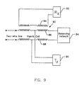
- the transmitter and receiver also include a hybrid circuit 80, which is shown in more detail in FIG. 9.
- the hybrid is a conventional communications circuit used to share transmitting and receiving functions on one pair of conductors.
- the hybrid includes a three-winding transformer 82 and an associated balancing network 84.
- One of the transformer windings 86 is connected in series with one conductor of a twisted pair, and another winding 88 is connected in series with the other conductor of the pair, which is terminated in the balancing network 84.
- the transmitter shown at 90, is connected to the center taps of these two windings 86, 88.
- the receiver indicated at 92, is connected to the third of the transformer windings 94.
- the impedance of the twisted pair and the balancing circuit are properly matched, all currents produced by the transmitted signal in the upper half of the hybrid transformer will be equal and in opposite directions, i.e. they will have no effect on the receiver 90. Also, in a properly balanced hybrid the received signals are inductively coupled to the receiver circuit, but are self-cancelling in the transmitter circuit.
- the channel bandwidth for each of the four channels of FIG. 7 is approximately 16 MHz. This results in better performance, as measured by lower crosstalk and intersymbol interference. Also, the time duration of one bit of data in each channel is doubled, from 16ns to 32ns.
- the obvious drawback of the embodiment of the invention shown in FIGS. 7 and 8 is that it requires more than twice as much hardware at each end of the transmission path, twice as many modulators and demodulators, and four additional hybrid circuits.
- clock signals for the demodulator will be recovered from the data signal itself. This can be done in a variety of ways. It will be apparent that the transmitted data signal normally has a strong signal component at the clock frequency. This can be recovered by appropriate filtering, and the demodulators can then be synchronized with this recovered clock signal. An alternate approach is to transmit the clock signal separately, but on the same channel as the data, as shown in the embodiments of FIGS. 10 and 11.
- the transmitter of FIG. 10 is similar to that of FIG. 7 except that it includes a signal summation circuit 100 between each modulator 16' and hybrid 80.
- the data signals from the modulator 16' are combined with a 25-MHz clock signal supplied on line 102.
- the resulting channel spectrum is shown in FIG. 10a, and includes the same 16-MHz bandwidth for the data signal, and a frequency line at 25 MHz for the clock signal.
- the receiver of FIG. 11 is similar to that of FIG. 8, except that it includes a stop-band filter 104 to prevent the clock signal from reaching the modified demodulator 32", and a 25-MHz passband filter 106 connected to extract the clock signal from the received signals.
- the 25-MHz clock signal is multiplied by five (in block 108) to provide a 125-MHz clock signal to the multiplexer 40', then divided by four (in block 110), to provide a 31.25-MHz clock signal for use in the demodulators 32".
- the demodulators 32'' include a phase adjustment circuit that aligns the clock signal in the middle of a received data bit interval.
- a phantom circuit is a well known communication device, in which two pairs of conductors provide a total of three communication channels. For example, if two pairs of twisted pairs are used in each direction, the use of phantom circuits provide a bandwidth reduction by a factor of three.
- the demultiplexer 14 in the transmitter must then be a 1:3 demultiplexer. Phantom circuits may also be used to detect cable breaks. For example, a 20-KHz signal can be injected into the communication channels through a phantom circuit at each transmitter, and detected at each receiver. Absence of the 20-KHz signal at any receiver is indicative of a cable break in the twisted-pair cable.
- the present invention represents a significant advance in the field of local area networks, in that high-speed networks designed to transmit through optical fibers, as in FDDI, may use twisted-pair cables instead, without degradation in performance for transmission distances up to about 100 meters.
- the invention provides for transmission of up to 125 Mb/s through four unshielded twisted pairs of conductors.
Landscapes
- Physics & Mathematics (AREA)
- Spectroscopy & Molecular Physics (AREA)
- Engineering & Computer Science (AREA)
- Computer Networks & Wireless Communication (AREA)
- Signal Processing (AREA)
- Dc Digital Transmission (AREA)
- Small-Scale Networks (AREA)
- Communication Control (AREA)
Description
- This invention relates generally to digital communication channels for local area networks and, more particularly, to techniques for using unshielded twisted pairs of conductors as a communication medium in a high-speed local area network. High-performance local area networks (LANs) typically use optical fiber or coaxial cable as the communication medium. For example one token ring network using optical fiber is known as the fiber distributed data interface (FDDI), and is intended for operation at a bandwidth of 125 megabits per second (Mb/s) over distances of about two kilometers. The physical layer medium dependent (PMD) sublayer protocol for FDDI is defined in an American National Standards Institute (ANSI) document designated X3T9.5/84-88. The other sublayer of the physical layer is known as the physical layer protocol (PHY) and is defined in ANSI X3.148-1988.
- A significant drawback to LANs using optical fiber as the communication medium is the relatively high cost of the optical fiber. Relatively slow LANs have been proposed using much cheaper unshielded twisted pair wiring, but prior to the present invention it has not been possible to use twisted pairs for typical FDDI bandwidths corresponding to transmission speeds in excess of 100 Mb/second.
- The present invention resides in a digital communication channel, and a corresponding method for its operation, using unshielded twisted pairs of conductors, through which a stream of binary data my be transmitted at rates of up to approximately 125 Mb/s or more. Briefly, and in general terms, the method of the invention comprises the steps of demultiplexing the binary data into at least two parallel channels, where each channel carries signals at a lower bandwidth than the original stream of binary data; encoding the binary data in each of the parallel channels into an n-level code in each channel to further reduce the bandwidth. The compressed-bandwidth signals in each channel are then transmitted over an unshielded twisted pair of conductors.
- At the receiving end of the transmission, the method includes the steps of compensating for the frequency response of each twisted pair of conductors; decoding the n-level signals received over each twisted pair of conductors into corresponding binary signals on multiple channels; and multiplexing the multiple channels into a single high-speed stream of binary data.
- US Patent 4,630,286 to Betts teaches method and apparatus for transmitting high-speed data from a transmitter to a receiver. In an effort to achieve synchronization of multiple telephone circuits, any differences in the transmission time between data channels are detected. Signals from the faster data channels are delayed so that at the receiving end, all signals are time-synchronized. For this purpose, differences in the transmission times are monitored. Signal modulation and phase shift in the data handled are discussed, but not bandwidth reduction.
- The invention, in its broad form, resides in a method and apparatus for transmitting a stream of high-speed binary data as recited in claims 1 and 13 respectively. Described hereinafter is a method for transmitting a stream of high-speed binary data over twisted pairs of unshielded conductors, comprising the steps of: demultiplexing the binary data into at least two parallel channels, where each channel carries signals at a lower bandwidth than the original stream of binary data; encoding the binary data in each of the parallel channels into an n-level code, where n is at least three and the bandwidth of the signals in each channel is further reduced by a factor of approximately two or more; lowpass filtering the n-level code in each channel to further reduce the bandwidth; and transmitting the signals in each channel over an unshielded twister pair of conductors.
- More specifically, the encoding step may include forming a three-level modified duobinary code, by subtractively combining the binary data stream with a time-delayed replica of the binary data stream. Preferably, the encoding step includes precoding the binary data, prior to the step of subtractively combining, to form a precoded binary data stream that (a) eliminates error propagation and (b) simplifies decoding.
- At the receiving end of the transmission, the decoding step includes transforming the received three-level modified duobinary code back into the binary code. If precoding has been used in the encoding steps, the decoding step is simply a rectifying step, wherein all nonzero levels are translated into a logical "1."
- In terms of apparatus, the invention comprises demultiplexing means, for separating the binary data into at least two parallel channels, where each channel carries signals at a lower bandwidth than the original stream of binary data but retaining a conventional FDDI coding format; modulation means, for encoding the binary data in each of the parallel channels into an n-level code, where n is at least three and the bandwidth of the signals in each channel is further reduced by a factor of approximately two or more; lowpass filter means, for further reducing the bandwidth of the n-level code in each channel; and means for transmitting the signals in each channel over an unshielded twisted pair of conductors.
- At the receiving end of the transmission, the apparatus further includes equalizer means, for compensating for the frequency response of each twisted pair of conductors; demodulator means, for decoding n-level signals received over each twisted pair of conductors into corresponding binary signals on multiple channels; and multiplexer means, for multiplexing the multiple channels into a single high-speed stream of binary data. As an alternative to the equalizer means and demodulator means, the apparatus may include a decoder based on the Viterbi algorithm.
- In the presently preferred embodiment of the invention, the modulation means includes means for forming a three-level modified duobinary code, by subtractively combining the binary data stream with a time-delayed replica of the binary data stream. Preferably, the modulation means also includes means for precoding the binary data, prior to the subtractively combining it with delayed data, to form a precoded binary data stream that eliminates error propagation and simplifies decoding. The demodulation means includes means for transforming the received three-level modified duobinary code back into the binary code.
- In an alternative embodiment of the invention, the apparatus includes means for demultiplexing the binary data into four parallel channels, where each channel carries signals at one-fourth the bandwidth of the original stream of binary data. The apparatus is otherwise similar to the embodiment described above, except that this version of the apparatus further includes a hybrid circuit for each twisted pair of conductors, to effect sharing of the pair between transmitting and receiving functions.
- In one form of the invention, clock signals are recovered from the received data stream. In another form of the invention, clock signals are transmitted over the same conductors as the data, but at a different frequency, and then recovered for use at the receiving end in decoding of the data signals.
- It will be appreciated from the foregoing that the present invention represents a significant advance in the field of digital data communication channels, particularly for use in local area networks. Specifically, the invention provides for the transmission of binary data at extremely high speeds, over unshielded twisted pairs of conductors usually applied to the transmission of much lower data rates. Use of demultiplexing, multi-level encoding and filtering of the digital signals results in a sufficient reduction in bandwidth to allow successful transmission over unshielded twisted pairs of conductors.
- A more detailed understanding of the invention may be had from the following description of preferred embodiments, given by way of example and to be understood in conjunction with the accompanying drawing, wherein:
- FIGURE 1 is block diagram of a transmitter in accordance with an embodiment of the present invention;
- FIG. 1a is a graph showing the spectrum of signals transmitted over one channel from the transmitter of FIG. 1;
- FIG. 2 is a block diagram of a receiver for use in conjunction with the transmitter of FIG. 1;
- FIG. 3 is a block diagram of a modulator used in the transmitter of FIG. 1;
- FIG. 4 is a block diagram of a demodulator used in the receiver of FIG. 2;
- FIG 5a-5f are timing diagrams showing a data stream at various stages of modulation and demodulation in the transmitter and receiver of FIGS. 1 and 2;
- FIG. 6 is a graph showing the frequency response of a twisted pair communication channel before and after equalization;
- FIG. 7 is a block diagram of an alternate embodiment of a transmitter;
- FIG. 7a is a graph showing the spectrum of signals transmitted over one channel from the transmitter of FIG. 7;
- FIG. 8 is a block diagram of a receiver for use in conjunction with the transmitter of FIG. 6;
- FIG. 9 is a block diagram of a hybrid circuit of the type used in the transmitters and receivers of FIGS. 7, 8, 10 and 11;
- FIG. 10 is a block diagram of yet another embodiment of a transmitter, similar to the one shown in FIG. 7 but in which a separated clock signal is transmitted with the data; and
- FIG. 11 is a block diagram of a receiver for use in conjunction with the transmitter of FIG. 10.
- As shown in the drawings for purposes of illustration, the present invention is concerned with a techniques for employing unshielded twisted pairs of conductors in local area networks that typically use optical fibers for the communication medium, such as the fiber distributed data interface (FDDI) token ring network. Unshielded twisted pairs have been proposed for use in token ring networks, but have been capable of only relatively low data transmission rates, such as 4 megabits per second (Mb/s). The present invention provides transmission rates of up to 125 Mb/s over unshielded twisted pairs up to 100 meters long.
- As described herein, this high level of performance is obtained by a combination of features. First, the data stream is demultiplexed into two data streams and transmitted over two or more pairs of conductors. Then, the binary data signals are converted to an n-level coding scheme, where n is three or more, for transmission over the twisted pairs. Finally, the n-level signals are filtered to further compress their bandwidth, but without loss of integrity of the data. These three features of the invention will be discussed in more detail with reference to block diagrams of a transmitter and a receiver structured in accordance with the invention.
- A basic difficulty encountered in using unshielded twisted pairs for the transmission of FDDI signals is that, for a transmission rate of 125 Mb/s, a channel bandwidth of about 90 MHz is required, but the typical bandwidth of a twisted pair is very much below this level. The low bandwidth results in a high intersymbol interference, which is a measure of the ability to distinguish and successfully decode successive encoded symbols transmitted over the channel. Intersymbol interference effectively limits the length of the channel to only a very short distance, which is not practical for most applications.
- The present invention uses a combination of approaches to compress the bandwidth or signal spectrum of FDDI signals such that they can be transmitted over twisted-pair channels of up to 100 meters in length.
- At a transmitter in accordance with the present invention, the FDDI signals are first demultiplexed with respect to time, i.e. the data signals, which are generated at a rate of 125 Mb/s, are split into two data streams at a 62.5 Mb/s data rate, as indicated at 10 and 12 in FIG. 1, by a
demultiplexer 14. Eachdata stream modulator driver twisted pair modulator drivers - In the receiver, shown in FIG. 2, signals on the unshielded
twisted pairs line receivers lines demodulators Clock recovery circuits demodulators demodulators demodulators multiplexer 40, which provides a single output online 42, carrying data at the 125 Mb/s rate. - The
modulator precoder section 44, a modifiedduobinary encoder section 46, and a low-pass filter 48. As is known in the digital communication art, duobinary encoding is a technique for increasing the bit rate that can be handled over a channel of given bandwidth. Duobinary encoding is effected by combining two successive binary signals to form a multilevel signal, which is further processed by a shaping filter. The resulting signal still has the disadvantage that it contains frequency components in the vicinity of zero frequency. This property is avoided in "modified" duobinary encoding, in which binary signals two time periods apart are combined subtractively. The result is a three-level signal with no significant components in the vicinity of zero frequency. A low-pass filter with a sine function response is employed after the encoding step. - The modified
duobinary encoder 46 includes adelay circuit 50, which interposes a delay equivalent to two data periods, and asubtractor circuit 52, in which the delayed binary data signals are subtracted from the undelayed incoming binary data signals, to produce a three-level modified duobinary code online 54. Modified duobinary code has the property that decoding it requires knowledge of prior values of the decoded signals. However, if the binary data signal is first processed by a precoder, before input to the modifiedduobinary encoder 46, the decoding logic is simplified and each duobinary input signal can be translated directly into binary code without reference to prior values of the translated binary code. - One form of precoding is indicated by the
precoder section 44, which includes another two-cycle delay circuit 56, and an exclusive ORgate 58. One input of the exclusive ORgate 58 is the uncoded binary data online delay circuit 56 takes its input signals from the output of the exclusive ORgate 58, and provides the second input to the exclusive OR gate. The output of the exclusive ORgate 58, online 60, provides precoded binary signals to thesubtractor circuit 52 and to delaycircuit 50. It will be understood that FIG. 3 is for purposes of explanation and that various other implementations are possible. For example, it will be apparent that one of thedelay circuits line 60. - Translation from binary code to modified duobinary code effects a bandwidth reduction by a factor of approximately two. Other multilevel encoding schemes were investigated as possibilities because, in general, a binary signal spectrum can be compressed by a factor of n by using 2n amplitude coding levels. However, as the number of levels is increased, immunity to crosstalk, as measured by the distance between adjacent levels, decreases. Moreover, the benefits obtained from spectrum compression may be outweighed by the decrease in immunity to crosstalk. For example, a change from 8-level modulation to 16-level modulation provides a bandwidth reduction of 25% and a corresponding reduction in crosstalk of about 2 dB (decibels), but the crosstalk immunity (the distance between adjacent levels) drops by 6 dB. Thus the 16-level system gives a worse performance than the 8-level system. The three-level modified duobinary approach was selected as providing optimum bandwidth compression, by a factor of two, without substantially decreasing crosstalk immunity. The three-level encoding approach uses the least number of coding levels needed to achieve a halving of the bandwidth, and has the additional advantage that it has no components in the vicinity of zero frequency.
- The last stage of processing after modified duobinary modulation is filtering in the
lowpass filter 48. This further reduces the bandwidth of the encoded signals, to a spectrum similar to the one shown in FIG. 1a. In the illustrative embodiment, each channel bandwidth is reduced to about 30 MHz for transmission through a twisted pair. This level is deliberately chosen to keep the bandwidth around or below 30 MHz. Above this threshold there are more stringent requirements imposed by the Federal Communications Commission (FCC). - The
demodulator equalizer 62 and arectifier 64. As will become apparent from an example to be described, the demodulation process is simply one of rectification if the modulator includes a precoding section. Therectifier 64 is basically a full-wave rectifier, and provides a logical "1" output signal when its input is either +1 or -1. If the input to therectifier 64 is a zero, the rectifier output is a logical "0." Theclock recovery circuit decision circuit 66, which further modifies the output of therectifier 64 and provides demodulator output to themultiplexer 40. - FIGS. 5a-5f together provide an example of the modified duobinary encoding and decoding process used in the invention. FIG. 5a is an illustrative waveform of a binary signal at the input of the modulator, on
line delay circuit 56 and applied to the other input of the exclusive ORcircuit 58. FIG. 5c is the resultant output of the exclusive ORgate 58, i.e. it represents the exclusive OR of the signals shown in FIGS. 5a and 5b. It will be noted that the waveform of FIG. 5b is delayed by two time cycles with respect to the output signal of FIG. 5c, which represents the precoded binary input signal. - The
subtractor circuit 52 subtracts the delayed input signal, which is the same as the one shown in FIG. 5b, from the undelayed input signal of FIG. 5c. The result is the three-level signal of FIG. 5d, which is then filtered in the low-pass filter 48, and transmitted onto one of thetwisted pairs - Decoding in the
demodulator TD +1 +1 -1 0 +1 0 0 -1 -1 +1 +1 -1 0 +1 0 DD 1 1 0 1 1 1 1 0 0 1 1 0 1 1 1 - It will be observed that this translation, the result of which is shown in FIG. 5e, yields the same waveform that was input to the encoding section (FIG. 5c).
- The other type of decoding is much simpler and is used when a precoding section is included in the modulator. In this case, each incoming bit of the transmitted three-level data can be translated to binary code without reference to time-displaced data. Specifically, levels of +1 and -1 in the transmitted data are translated into a logical "1" and a zero level is translated into a logical "0," as shown below:
TD +1 +1 -1 0 +1 0 0 -1 -1 +1 +1 -1 0 +1 0 DD 1 1 1 0 1 0 0 1 1 1 1 1 0 1 0 - The resulting decoded data is shown in FIG. 5f, which is the same as the waveform (FIG. 5a) that was input to the precoding section of the modulator.
- An important advantage of the invention is that it retains the conventional signal format for transmission on a fiber distributed data interface (FDDI) token ring network. In the FDDI system, signals are presented to the physical protocol layer coded in accordance with NRZI coding. NRZI stands for "nonreturn to zero invert on ones." What this means is that a polarity transition in the signal represents a logical "1" and the absence of a polarity transition represents a logical "0." Further, the FDDI formats signals into five-bit code groups. Each transmitted symbol, which may be a four-bit data symbol, or a control symbol, is represented as a five-bit sequence of NRZI bits. This is sometimes referred to as 4B/5B NRZI coding. The coding format is discussed in American National Standard ANSI X3.148-1988 defining the physical layer protocol (PHY) for FDDI. One significant advantage of 4B/5B NRZI coding is that it guarantees a minimum signal transition rate, and therefore minimizes direct-current components and ensures that a clock signal can be recovered. To guarantee these properties, 4B/5B NRZI encoding precludes the use of some five-bit code groups, having too few transitions or too many consecutive zeros. The present invention retains the 4B/5B NRZI format, and therefore retains the advantages of this type of coding in the FDDI.
- The frequency response of an unshielded twisted pair of conductors is shown diagrammatically at 70 in FIG. 6. As the frequency of transmission increases, the response or output from the twisted pair decreases. The principal function of the equalizer 62 (FIG. 4) is to compensate for this fall-off in response at higher frequencies. Accordingly, the
equalizer 62 is designed to have a frequency response inverse to that of the twisted pair, as shown at 72 in FIG. 6. The goal is to provide a composite frequency response that is substantially uniform with frequency over a spectrum of interest, as shown at 74. Since the frequency response of the twisted pair will depend on its length, the equalizer will not provide perfect compensation for all lengths of cable. As a compromise, the equalizer should be designed to provide compensation for a most commonly used cable runlength, or for one half of the maximum runlength. In general, equalization results in an increase in crosstalk level. If the crosstalk becomes a limiting factor, it is preferable to use a decoder (not shown) based on the Viterbi algorithm, to replace theequalizer 62 and therectifier 64. A description of the Viterbi algorithm may be found in "Data Communications, Networks, and Systems," Thomas C. Bartee, Editor-in-Chief, published by Howard W. Sams & Co., Indianapolis, Indiana (1985). - FIGS. 7 and 8 show an alternative embodiment of the invention in which four twisted pairs are used for both directions of transmission. The transmitter contains a 1:4 demultiplexer 14' to provide four data streams of 31.25 Mb/s, and the receiver contains a 4:1 multiplexer 40'. Modulator driver circuits 16', line receivers 24', demodulators 32' and clock recovery circuits 36' are of similar design to their counterparts in FIGS. 1 and 2. The transmitter and receiver also include a
hybrid circuit 80, which is shown in more detail in FIG. 9. - The hybrid is a conventional communications circuit used to share transmitting and receiving functions on one pair of conductors. The hybrid includes a three-winding
transformer 82 and an associatedbalancing network 84. One of thetransformer windings 86 is connected in series with one conductor of a twisted pair, and another winding 88 is connected in series with the other conductor of the pair, which is terminated in thebalancing network 84. The transmitter, shown at 90, is connected to the center taps of these twowindings transformer windings 94. If the impedance of the twisted pair and the balancing circuit are properly matched, all currents produced by the transmitted signal in the upper half of the hybrid transformer will be equal and in opposite directions, i.e. they will have no effect on thereceiver 90. Also, in a properly balanced hybrid the received signals are inductively coupled to the receiver circuit, but are self-cancelling in the transmitter circuit. - As shown diagrammatically in FIG. 7a, the channel bandwidth for each of the four channels of FIG. 7 is approximately 16 MHz. This results in better performance, as measured by lower crosstalk and intersymbol interference. Also, the time duration of one bit of data in each channel is doubled, from 16ns to 32ns. The obvious drawback of the embodiment of the invention shown in FIGS. 7 and 8 is that it requires more than twice as much hardware at each end of the transmission path, twice as many modulators and demodulators, and four additional hybrid circuits.
- In the description thus far, it has been assumed that clock signals for the demodulator will be recovered from the data signal itself. This can be done in a variety of ways. It will be apparent that the transmitted data signal normally has a strong signal component at the clock frequency. This can be recovered by appropriate filtering, and the demodulators can then be synchronized with this recovered clock signal. An alternate approach is to transmit the clock signal separately, but on the same channel as the data, as shown in the embodiments of FIGS. 10 and 11.
- The transmitter of FIG. 10 is similar to that of FIG. 7 except that it includes a
signal summation circuit 100 between each modulator 16' andhybrid 80. In thesummation circuit 100, the data signals from the modulator 16' are combined with a 25-MHz clock signal supplied online 102. The resulting channel spectrum is shown in FIG. 10a, and includes the same 16-MHz bandwidth for the data signal, and a frequency line at 25 MHz for the clock signal. - The receiver of FIG. 11 is similar to that of FIG. 8, except that it includes a stop-
band filter 104 to prevent the clock signal from reaching the modifieddemodulator 32", and a 25-MHz passband filter 106 connected to extract the clock signal from the received signals. The 25-MHz clock signal is multiplied by five (in block 108) to provide a 125-MHz clock signal to the multiplexer 40', then divided by four (in block 110), to provide a 31.25-MHz clock signal for use in thedemodulators 32". The demodulators 32'' include a phase adjustment circuit that aligns the clock signal in the middle of a received data bit interval. - Other variations of the invention are possible, including the use of phantom circuits to provide additional channels. A phantom circuit is a well known communication device, in which two pairs of conductors provide a total of three communication channels. For example, if two pairs of twisted pairs are used in each direction, the use of phantom circuits provide a bandwidth reduction by a factor of three. The
demultiplexer 14 in the transmitter must then be a 1:3 demultiplexer. Phantom circuits may also be used to detect cable breaks. For example, a 20-KHz signal can be injected into the communication channels through a phantom circuit at each transmitter, and detected at each receiver. Absence of the 20-KHz signal at any receiver is indicative of a cable break in the twisted-pair cable. - It will be appreciated from the foregoing that the present invention represents a significant advance in the field of local area networks, in that high-speed networks designed to transmit through optical fibers, as in FDDI, may use twisted-pair cables instead, without degradation in performance for transmission distances up to about 100 meters. In particular, the invention provides for transmission of up to 125 Mb/s through four unshielded twisted pairs of conductors. It will also be appreciated that, although several embodiments of the invention have been described in detail for purposes of illustration, various modifications may be made without departing from the scope of the invention. Accordingly, the invention is not to be limited except as by the appended claims.
Claims (20)
- A method for transmitting a stream of high-speed binary data over twisted pairs of conductors (10,12) operating as baseband communications channels, the method comprising the steps of:demultiplexing the binary data into at least two parallel channels (10,12), wherein each channel carries demultiplexed binary data signals at a lower bandwidth than the original stream of binary data;encoding (16,18) the binary data in each of the parallel channels into an n-level amplitude-modulated code, wherein n is at least three and the bandwidth of the signals in each channel is further reduced by a factor of approximately two or more;lowpass filtering (48) the n-level code in each channel to further reduce the bandwidth; andtransmitting the signals in each channel over an unshielded twisted pair of conductors operating as a baseband communication channel.
- A method as defined in claim 1, and further comprising the steps of:compensating for the frequency response of each twisted pair of conductors;decoding n-level signals received over each twisted pair of conductors into corresponding binary signals on multiple channels; andmultiplexing the multiple channels into a single high-speed stream of binary data.
- A method as defined in claim 1, wherein:
the encoding step includes forming a three-level modified duobinary code. - A method as defined in claim 3, wherein the step of forming a three-level modified duobinary code includes:
subtractively combining the binary data stream with a time-delayed replica of the binary data stream, to yield the modified duobinary code. - A method as defined in claim 4, wherein the step of forming a three-level modified duobinary code further includes:
precoding the binary data, prior to the step of subtractively combining, to form a precoded binary data stream that eliminates error propagation and simplifies decoding. - A method as defined in claim 2, wherein:the encoding step includes forming a three-level modified duobinary code; andthe decoding step includes transforming a received three-level modified duobinary code into a binary code.
- A method as defined in claim 6, wherein the step of forming a three-level modified duobinary code includes:
subtractively combining the binary data stream with a time-delayed replica of the binary data stream, to yield the modified duobinary code. - A method as defined in claim 7, wherein the step of transforming the three-level modified duobinary code into a binary code includes:
rectifying the three-level code. - A method as defined in claim 8, wherein the step of forming a three-level modified duobinary code further includes:
precoding the binary data, prior to the step of subtractively combining, to form a precoded binary data stream that eliminates error propagation and simplifies decoding. - A method as defined in any of the preceding claims, further characterized by:receiving the transmitted signals;compensating for the frequency response of each twisted pair of conductors;decoding the 3-level signals received over each twisted pair of conductors into corresponding binary signals on two channels; andmultiplexing the two channels into a single high speed stream of binary data.
- A method as defined in claim 10, wherein:the original data stream is processed at a rate of approximately 125 megabits per second;the demultiplexing step provides two channels at approximately 62.5 megabits per second;the encoding step reduces the effective speed of each channel to approximately 31.25 megabits per second; andthe filtering step reduces the bandwidth of each channel to approximately 30 megahertz.
- A method as defined in claim 10, wherein:the method is used in a fiber distributed data interface (FDDI) communication network, using a signal format in which each four-bit data code is encoded into a five-bit NRZI (nonreturn to zero invert on ones) code in accordance with coding scheme referred to as 4B/5B; andthe demultiplexing step retains the 4B/5B format in each of its resultant channels.
- Digital signal communication apparatus for transmitting a stream of high-speed binary data over twisted pairs of conductors (20, 22) operating as baseband communication channels, the apparatus comprising:demultiplexing means (14), for separating the binary data into at least two parallel channels (10, 12), wherein each channel carries demultiplexed binary data signals at a lower bandwidth than the original stream of binary data;modulation means (16, 18) for encoding the binary data in each of the parallel channels into an n-level amplitude-modulated code, wherein n is at least three and the bandwidth of the signals in each channel is further reduced by a factor of approximately two or more;lowpass filter means (48) for further reducing the bandwidth of the n-level code in each channel; andmeans (14') for transmitting the signals in each channel over an unshielded twisted pair of conductors operating as a baseband communication channel.
- Apparatus as defined in claim 13, and further comprising:equalizer means (62), for compensating for the frequency response of each twisted pair of conductors;demodulator means, for decoding n-level signals received over each twisted pair of conductors into corresponding binary signals on multiple channels; andmultiplexer means (40), for multiplexing the multiple channels into a single high-speed stream of binary data.
- Apparatus as defined in claim 13, wherein:
the modulation means includes means for forming three-level modified duobinary code. - Apparatus as defined in claim 15, wherein the means for forming a three-level modified duobinary code includes:
means for subtractively combining the binary data stream with a time-delayed replica of the binary data stream, to yield the modified duobinary code. - Apparatus as defined in claim 15, wherein the means for forming a three-level modified duobinary code further includes:
means for precoding the binary data, prior to the subtractively combining it with delayed data, to form a precoded binary data stream that simplifies decoding. - Apparatus as defined in claim 14, wherein:the modulation means includes means for forming a three-level modified duobinary code; andthe demodulation means includes means for transforming a received three-level modified duobinary code into a binary code.
- Apparatus as defined in claim 18, wherein the means for transforming the three-level modified duobinary code into a binary code includes:
means for rectifying the three-level code. - Apparatus as defined in claim 19, wherein the means for forming a three-level modified duobinary code further includes:
means for precoding the binary data, prior to the step of subtractively combining, to form a precoded binary data stream that simplifies decoding.
Applications Claiming Priority (2)
| Application Number | Priority Date | Filing Date | Title |
|---|---|---|---|
| US07/545,310 US5119402A (en) | 1990-06-26 | 1990-06-26 | Method and apparatus for transmission of local area network signals over unshielded twisted pairs |
| US545310 | 2000-04-07 |
Publications (3)
| Publication Number | Publication Date |
|---|---|
| EP0471945A2 EP0471945A2 (en) | 1992-02-26 |
| EP0471945A3 EP0471945A3 (en) | 1993-05-19 |
| EP0471945B1 true EP0471945B1 (en) | 1997-08-27 |
Family
ID=24175712
Family Applications (1)
| Application Number | Title | Priority Date | Filing Date |
|---|---|---|---|
| EP91110387A Expired - Lifetime EP0471945B1 (en) | 1990-06-26 | 1991-06-24 | Method and apparatus for transmission of local area network signals over unshielded twisted pairs |
Country Status (5)
| Country | Link |
|---|---|
| US (1) | US5119402A (en) |
| EP (1) | EP0471945B1 (en) |
| JP (1) | JPH04233851A (en) |
| CA (1) | CA2045340A1 (en) |
| DE (1) | DE69127415T2 (en) |
Cited By (1)
| Publication number | Priority date | Publication date | Assignee | Title |
|---|---|---|---|---|
| US8855147B2 (en) | 2001-03-14 | 2014-10-07 | At&T Intellectual Property Ii, L.P. | Devices and methods to communicate data streams |
Families Citing this family (59)
| Publication number | Priority date | Publication date | Assignee | Title |
|---|---|---|---|---|
| US5208804A (en) * | 1990-10-30 | 1993-05-04 | Motorola, Inc. | Flexible-bandwidth radio |
| US5255287A (en) * | 1991-06-28 | 1993-10-19 | Digital Equipment Corporation | Transceiver apparatus and methods |
| US5412691A (en) * | 1991-06-28 | 1995-05-02 | Digital Equipment Corporation | Method and apparatus for equalization for transmission over a band-limited channel |
| US5408473A (en) * | 1992-03-03 | 1995-04-18 | Digital Equipment Corporation | Method and apparatus for transmission of communication signals over two parallel channels |
| US5341400A (en) * | 1992-07-29 | 1994-08-23 | 3Com Corporation | Method and apparatus for automatically sensing and configuring a termination in a bus-based network |
| US5438571A (en) * | 1992-11-06 | 1995-08-01 | Hewlett-Packard Company | High speed data transfer over twisted pair cabling |
| GB9314479D0 (en) * | 1992-11-06 | 1993-08-25 | Hewlett Packard Co | Encoding data |
| US5550836A (en) * | 1992-11-06 | 1996-08-27 | Hewlett-Packard Company | High speed data transfer over twisted pair cabling |
| US5408500A (en) * | 1993-02-17 | 1995-04-18 | Digital Equipment Corporation | Method and apparatus for transmission of local area network signals over a single unshielded twisted pair |
| US5444737A (en) * | 1993-05-05 | 1995-08-22 | National Semiconductor Corporation | Wireless data transceiver |
| US5533056A (en) * | 1993-05-05 | 1996-07-02 | National Semiconductor Corporation | Data encoder/decoder for data transceiver |
| GB9314480D0 (en) * | 1993-07-09 | 1993-08-25 | Hewlett Packard Co | Encoding data |
| US5796781A (en) * | 1993-07-09 | 1998-08-18 | Technitrol, Inc. | Data receiver having bias restoration |
| ES2078854B1 (en) * | 1993-08-06 | 1997-11-16 | Alcatel Standard Electrica | DIGITAL TRANSMISSION SYSTEM IN LINES OF TRANSMISSION OF BRAIDED PAIRS. |
| US5544323A (en) * | 1993-09-23 | 1996-08-06 | Standard Microsystems Corp. | High bit rate ethernet connection |
| US5619539A (en) * | 1994-02-28 | 1997-04-08 | International Business Machines Corporation | Data detection methods and apparatus for a direct access storage device |
| CA2120697C (en) * | 1994-04-06 | 1999-08-10 | Vernon Robert Little | Pair division multiplexer for digital communications |
| US5553097A (en) * | 1994-06-01 | 1996-09-03 | International Business Machines Corporation | System and method for transporting high-bandwidth signals over electrically conducting transmission lines |
| DE4444654B4 (en) * | 1994-12-15 | 2004-12-30 | Philips Intellectual Property & Standards Gmbh | Transmission system for the transmission of two binary signals, multiplexer and demultiplexer |
| US5651001A (en) * | 1994-12-22 | 1997-07-22 | Intel Corporation | Method and apparatus for full duplex signaling |
| GB9506470D0 (en) * | 1995-03-29 | 1995-05-17 | Sgs Thomson Microelectronics | 5b4t coding scheme |
| GB9506471D0 (en) * | 1995-03-29 | 1995-05-17 | Sgs Thomson Microelectronics | Coding scheme for transmitting data |
| US5828733A (en) * | 1995-04-03 | 1998-10-27 | Advanced Micro Devices, Inc. | Method and arrangement for increasing data transmisssion rate over telephone cable |
| US5734293A (en) * | 1995-06-07 | 1998-03-31 | Linear Technology Corporation | Fast current feedback amplifiers and current-to-voltage converters and methods maintaining high DC accuracy over temperature |
| US5598413A (en) * | 1995-07-10 | 1997-01-28 | Adtran, Inc. | Four-wire, half-rate architecture with embedded differential delay compensation for extending range of basic rate ISDN communications |
| US6470405B2 (en) * | 1995-10-19 | 2002-10-22 | Rambus Inc. | Protocol for communication with dynamic memory |
| WO1997034390A1 (en) * | 1996-03-13 | 1997-09-18 | Analog Devices, Inc. | High speed data communication over unshielded twisted pair |
| US6385203B2 (en) | 1996-03-29 | 2002-05-07 | Cisco Technology, Inc. | Communication server apparatus and method |
| US5668857A (en) * | 1996-03-29 | 1997-09-16 | Netspeed, Inc. | Communication server apparatus and method |
| US6160843A (en) * | 1996-03-29 | 2000-12-12 | Cisco Technology, Inc. | Communication server apparatus providing XDSL services and method |
| US5781598A (en) * | 1996-08-14 | 1998-07-14 | Hardy, Iii; Harmon S. | System and method of asynchronous data transfer through a plurality of modems |
| US5940403A (en) * | 1996-11-07 | 1999-08-17 | Adtran, Inc. | Quarter-rate 2B1Q ISDN architecture with embedded differential delay compensation for extending range of DDS communications |
| US6262993B1 (en) | 1996-11-08 | 2001-07-17 | Kevin Kirmse | Computer and peripheral networking device permitting the practical use of buffer insertion-based networks while communicating over unshielded twisted pair conductive media |
| US6163599A (en) * | 1997-03-20 | 2000-12-19 | Cisco Technology, Inc. | Communication server apparatus and method |
| US6058479A (en) * | 1997-05-05 | 2000-05-02 | Lancast, Inc. | Redundant path data switch and media translator |
| US6266379B1 (en) * | 1997-06-20 | 2001-07-24 | Massachusetts Institute Of Technology | Digital transmitter with equalization |
| US6366644B1 (en) | 1997-09-15 | 2002-04-02 | Cisco Technology, Inc. | Loop integrity test device and method for digital subscriber line (XDSL) communication |
| US5999565A (en) * | 1997-10-15 | 1999-12-07 | Cisco Technology, Inc. | Data communication using a modifiable number of XDSL modems |
| US6252878B1 (en) | 1997-10-30 | 2001-06-26 | Cisco Technology, Inc. | Switched architecture access server |
| FR2775526B1 (en) * | 1998-02-27 | 2000-04-21 | Sgs Thomson Microelectronics | TEST DEVICE FOR PRODUCING THE DYNAMIC CHARACTERISTICS OF COMPONENTS USING SERIES TRANSMISSIONS |
| US6278728B1 (en) | 1998-03-18 | 2001-08-21 | Cisco Technology, Inc. | Remote XDSL transceiver unit and method of operation |
| WO1999053627A1 (en) | 1998-04-10 | 1999-10-21 | Chrimar Systems, Inc. Doing Business As Cms Technologies | System for communicating with electronic equipment on a network |
| US6181572B1 (en) | 1998-06-19 | 2001-01-30 | Cisco Technology, Inc. | Digital subscriber line (xDSL) modem having a multi-layer electromagnetic shield and method of manufacture |
| US6239672B1 (en) | 1998-06-29 | 2001-05-29 | Cisco Technology, Inc. | Wall mount filter for a digital subscriber line (xDSL) network and methods of installation and manufacture |
| US6535520B1 (en) | 1998-08-14 | 2003-03-18 | Cisco Technology, Inc. | System and method of operation for managing data communication between physical layer devices and ATM layer devices |
| US6381245B1 (en) | 1998-09-04 | 2002-04-30 | Cisco Technology, Inc. | Method and apparatus for generating parity for communication between a physical layer device and an ATM layer device |
| JP4141028B2 (en) * | 1998-11-25 | 2008-08-27 | 富士通株式会社 | Code conversion circuit for optical duobinary transmission, and optical transmitter and optical receiver using the same |
| US6522668B1 (en) | 1998-11-30 | 2003-02-18 | Cisco Technology, Inc. | System and method for special signaling with customer premises equipment |
| US6115226A (en) * | 1998-12-07 | 2000-09-05 | Cisco Technology, Inc. | Apparatus for lightning strike survivability and post-strike operability |
| US5999540A (en) * | 1998-12-22 | 1999-12-07 | Cisco Technology, Inc. | Rate adaptive XDSL communication system and method |
| US6161161A (en) * | 1999-01-08 | 2000-12-12 | Cisco Technology, Inc. | System and method for coupling a local bus to a peripheral component interconnect (PCI) bus |
| US6658049B1 (en) | 1999-01-12 | 2003-12-02 | Cisco Technology, Inc. | xDSL repeater system and method |
| US6553075B1 (en) | 1999-01-12 | 2003-04-22 | Cisco Technology, Inc. | Method and apparatus for determining crosstalk |
| KR100325323B1 (en) * | 1999-03-10 | 2002-03-04 | 원 진 | Local Digital Subscriber's Line; LDSL |
| JP3705102B2 (en) * | 2000-09-14 | 2005-10-12 | 日本電気株式会社 | Communication device |
| US6950414B1 (en) * | 2000-10-17 | 2005-09-27 | Ericsson Inc. | Cable carrying communications data and timing data to radio heads |
| US6738173B2 (en) * | 2001-06-26 | 2004-05-18 | Andrew Bonthron | Limiting amplifier modulator driver |
| US8396137B1 (en) * | 2010-11-02 | 2013-03-12 | The Boeing Company | Redundant data bus |
| US9621254B2 (en) * | 2012-09-21 | 2017-04-11 | Spatial Digital Systems, Inc. | Communications architectures via UAV |
Family Cites Families (11)
| Publication number | Priority date | Publication date | Assignee | Title |
|---|---|---|---|---|
| NL170688C (en) * | 1976-06-28 | 1982-12-01 | Philips Nv | DEVICE FOR SIMULTANEOUS TWO WAY DATA TRANSMISSION ON TWO WIRE CONNECTIONS. |
| GB1592556A (en) * | 1976-10-28 | 1981-07-08 | Rixon | Quadrature-amplitude-modulation data transmission systems and transmitters |
| US4383316A (en) * | 1980-04-14 | 1983-05-10 | Bell Telephone Laboratories, Incorporated | Apparatus for and method of collating partitioned time disordered synchronous data streams |
| US4571734A (en) * | 1983-08-05 | 1986-02-18 | International Business Machines Corporation | Method and apparatus for decoding the output signal of a partial-response class-IV communication or recording-device channel |
| GB8407223D0 (en) * | 1984-03-20 | 1984-04-26 | British Telecomm | Broadband digital transmission systems |
| US4630286A (en) * | 1984-10-10 | 1986-12-16 | Paradyne Corporation | Device for synchronization of multiple telephone circuits |
| US4734920A (en) * | 1984-10-10 | 1988-03-29 | Paradyne Corporation | High speed modem for multiple communication circuits |
| JPS6256040A (en) * | 1985-09-04 | 1987-03-11 | Fujitsu Ltd | Delay time compensation circuit |
| JPH0748675B2 (en) * | 1987-08-21 | 1995-05-24 | 日本電気株式会社 | Digital transmission system |
| US4862456A (en) * | 1988-05-04 | 1989-08-29 | The United States Of America As Represented By The Secretary Of The Navy | High speed modem |
| US4980897A (en) * | 1988-08-12 | 1990-12-25 | Telebit Corporation | Multi-channel trellis encoder/decoder |
-
1990
- 1990-06-26 US US07/545,310 patent/US5119402A/en not_active Expired - Lifetime
-
1991
- 1991-06-24 DE DE69127415T patent/DE69127415T2/en not_active Expired - Fee Related
- 1991-06-24 JP JP3151304A patent/JPH04233851A/en active Pending
- 1991-06-24 EP EP91110387A patent/EP0471945B1/en not_active Expired - Lifetime
- 1991-06-25 CA CA002045340A patent/CA2045340A1/en not_active Abandoned
Cited By (1)
| Publication number | Priority date | Publication date | Assignee | Title |
|---|---|---|---|---|
| US8855147B2 (en) | 2001-03-14 | 2014-10-07 | At&T Intellectual Property Ii, L.P. | Devices and methods to communicate data streams |
Also Published As
| Publication number | Publication date |
|---|---|
| DE69127415D1 (en) | 1997-10-02 |
| CA2045340A1 (en) | 1991-12-27 |
| DE69127415T2 (en) | 1998-04-02 |
| EP0471945A2 (en) | 1992-02-26 |
| EP0471945A3 (en) | 1993-05-19 |
| US5119402A (en) | 1992-06-02 |
| JPH04233851A (en) | 1992-08-21 |
Similar Documents
| Publication | Publication Date | Title |
|---|---|---|
| EP0471945B1 (en) | Method and apparatus for transmission of local area network signals over unshielded twisted pairs | |
| US5856980A (en) | Baseband encoding method and apparatus for increasing the transmission rate over a communication medium | |
| US7133425B2 (en) | Communication system | |
| US8229035B2 (en) | Apparatus for, and method of, processing signals transmitted over a local area network | |
| US7180959B2 (en) | Technique for utilizing spare bandwidth resulting from the use of a code in a multi-level signaling system | |
| KR102517583B1 (en) | High speed communications system | |
| US6009120A (en) | Multi-dimensional combined equalizer and decoder | |
| CA2192913C (en) | Reformatting of variable rate data for fixed rate communication | |
| US10484046B1 (en) | Systems and methods for a twisted pair transceiver with correlation detection | |
| JPH02172333A (en) | Communication system and communication method | |
| JPH03503824A (en) | Digital data in voice communications | |
| US20040008794A1 (en) | Method and apparatus for constellation shaping | |
| US5422919A (en) | EMI suppression coding | |
| US5408500A (en) | Method and apparatus for transmission of local area network signals over a single unshielded twisted pair | |
| CN112217755B (en) | Parallel channel skew for enhanced error correction | |
| US5216714A (en) | Method and apparatus for controlling the spectral content of a data stream | |
| JPH09200283A (en) | Modem device | |
| US5500892A (en) | Echo canceller | |
| US20050099325A1 (en) | Technique for improving the quality of digital signals in a multi-level signaling system | |
| EP0299639A2 (en) | Digital data communications system | |
| US5058129A (en) | Two-wire digital transmission loop | |
| US20090016382A1 (en) | System and Method for High-Speed Applications over a Serial Multi-Drop Communication Network | |
| US20040047283A1 (en) | FDM signals crosstalk cancellation technique | |
| US20060015790A1 (en) | Low overhead coding techniques | |
| Ginzburg et al. | FDDI over unshielded twisted pairs |
Legal Events
| Date | Code | Title | Description |
|---|---|---|---|
| PUAI | Public reference made under article 153(3) epc to a published international application that has entered the european phase |
Free format text: ORIGINAL CODE: 0009012 |
|
| 17P | Request for examination filed |
Effective date: 19910724 |
|
| AK | Designated contracting states |
Kind code of ref document: A2 Designated state(s): DE FR GB IT NL |
|
| PUAL | Search report despatched |
Free format text: ORIGINAL CODE: 0009013 |
|
| AK | Designated contracting states |
Kind code of ref document: A3 Designated state(s): DE FR GB IT NL |
|
| 17Q | First examination report despatched |
Effective date: 19960312 |
|
| GRAG | Despatch of communication of intention to grant |
Free format text: ORIGINAL CODE: EPIDOS AGRA |
|
| GRAH | Despatch of communication of intention to grant a patent |
Free format text: ORIGINAL CODE: EPIDOS IGRA |
|
| GRAH | Despatch of communication of intention to grant a patent |
Free format text: ORIGINAL CODE: EPIDOS IGRA |
|
| GRAA | (expected) grant |
Free format text: ORIGINAL CODE: 0009210 |
|
| AK | Designated contracting states |
Kind code of ref document: B1 Designated state(s): DE FR GB IT NL |
|
| REF | Corresponds to: |
Ref document number: 69127415 Country of ref document: DE Date of ref document: 19971002 |
|
| ITF | It: translation for a ep patent filed |
Owner name: STUDIO TORTA S.R.L. |
|
| ET | Fr: translation filed | ||
| PGFP | Annual fee paid to national office [announced via postgrant information from national office to epo] |
Ref country code: NL Payment date: 19980527 Year of fee payment: 8 |
|
| PLBE | No opposition filed within time limit |
Free format text: ORIGINAL CODE: 0009261 |
|
| STAA | Information on the status of an ep patent application or granted ep patent |
Free format text: STATUS: NO OPPOSITION FILED WITHIN TIME LIMIT |
|
| 26N | No opposition filed | ||
| PG25 | Lapsed in a contracting state [announced via postgrant information from national office to epo] |
Ref country code: NL Free format text: LAPSE BECAUSE OF NON-PAYMENT OF DUE FEES Effective date: 20000101 |
|
| NLV4 | Nl: lapsed or anulled due to non-payment of the annual fee |
Effective date: 20000101 |
|
| REG | Reference to a national code |
Ref country code: GB Ref legal event code: 732E |
|
| REG | Reference to a national code |
Ref country code: GB Ref legal event code: IF02 |
|
| PGFP | Annual fee paid to national office [announced via postgrant information from national office to epo] |
Ref country code: DE Payment date: 20070731 Year of fee payment: 17 |
|
| PGFP | Annual fee paid to national office [announced via postgrant information from national office to epo] |
Ref country code: IT Payment date: 20070628 Year of fee payment: 17 |
|
| PGFP | Annual fee paid to national office [announced via postgrant information from national office to epo] |
Ref country code: FR Payment date: 20080617 Year of fee payment: 18 |
|
| PG25 | Lapsed in a contracting state [announced via postgrant information from national office to epo] |
Ref country code: DE Free format text: LAPSE BECAUSE OF NON-PAYMENT OF DUE FEES Effective date: 20090101 |
|
| PG25 | Lapsed in a contracting state [announced via postgrant information from national office to epo] |
Ref country code: IT Free format text: LAPSE BECAUSE OF NON-PAYMENT OF DUE FEES Effective date: 20080624 |
|
| PGFP | Annual fee paid to national office [announced via postgrant information from national office to epo] |
Ref country code: GB Payment date: 20090625 Year of fee payment: 19 |
|
| REG | Reference to a national code |
Ref country code: FR Ref legal event code: ST Effective date: 20100226 |
|
| PG25 | Lapsed in a contracting state [announced via postgrant information from national office to epo] |
Ref country code: FR Free format text: LAPSE BECAUSE OF NON-PAYMENT OF DUE FEES Effective date: 20090630 |
|
| GBPC | Gb: european patent ceased through non-payment of renewal fee |
Effective date: 20100624 |
|
| PG25 | Lapsed in a contracting state [announced via postgrant information from national office to epo] |
Ref country code: GB Free format text: LAPSE BECAUSE OF NON-PAYMENT OF DUE FEES Effective date: 20100624 |