EP0465264B1 - Metal film forming method - Google Patents
Metal film forming method Download PDFInfo
- Publication number
- EP0465264B1 EP0465264B1 EP91306118A EP91306118A EP0465264B1 EP 0465264 B1 EP0465264 B1 EP 0465264B1 EP 91306118 A EP91306118 A EP 91306118A EP 91306118 A EP91306118 A EP 91306118A EP 0465264 B1 EP0465264 B1 EP 0465264B1
- Authority
- EP
- European Patent Office
- Prior art keywords
- monocrystalline
- film
- state
- ion implantation
- heating
- Prior art date
- Legal status (The legal status is an assumption and is not a legal conclusion. Google has not performed a legal analysis and makes no representation as to the accuracy of the status listed.)
- Expired - Lifetime
Links
- 238000000034 method Methods 0.000 title claims abstract description 60
- 229910052751 metal Inorganic materials 0.000 title claims abstract description 33
- 239000002184 metal Substances 0.000 title claims abstract description 33
- 238000010438 heat treatment Methods 0.000 claims abstract description 117
- 229910052782 aluminium Inorganic materials 0.000 claims abstract description 51
- XAGFODPZIPBFFR-UHFFFAOYSA-N aluminium Chemical compound [Al] XAGFODPZIPBFFR-UHFFFAOYSA-N 0.000 claims abstract description 21
- 239000000758 substrate Substances 0.000 claims description 92
- 238000005468 ion implantation Methods 0.000 claims description 75
- 238000009413 insulation Methods 0.000 claims description 71
- 238000010894 electron beam technology Methods 0.000 claims description 48
- 238000005229 chemical vapour deposition Methods 0.000 claims description 37
- 239000013078 crystal Substances 0.000 claims description 33
- 238000000151 deposition Methods 0.000 claims description 30
- 239000004065 semiconductor Substances 0.000 claims description 15
- UFHFLCQGNIYNRP-UHFFFAOYSA-N Hydrogen Chemical compound [H][H] UFHFLCQGNIYNRP-UHFFFAOYSA-N 0.000 claims description 12
- 239000007789 gas Substances 0.000 claims description 12
- -1 alkylaluminum hydride Chemical class 0.000 claims description 8
- 230000005855 radiation Effects 0.000 claims description 7
- 230000006698 induction Effects 0.000 claims 1
- 239000010408 film Substances 0.000 description 194
- VYPSYNLAJGMNEJ-UHFFFAOYSA-N Silicium dioxide Chemical compound O=[Si]=O VYPSYNLAJGMNEJ-UHFFFAOYSA-N 0.000 description 66
- 238000002128 reflection high energy electron diffraction Methods 0.000 description 62
- 229910018125 Al-Si Inorganic materials 0.000 description 35
- 229910018520 Al—Si Inorganic materials 0.000 description 35
- 229910052681 coesite Inorganic materials 0.000 description 32
- 229910052906 cristobalite Inorganic materials 0.000 description 32
- 239000000377 silicon dioxide Substances 0.000 description 32
- 229910052682 stishovite Inorganic materials 0.000 description 32
- 229910052905 tridymite Inorganic materials 0.000 description 32
- 150000002500 ions Chemical class 0.000 description 28
- 230000008021 deposition Effects 0.000 description 24
- 230000009466 transformation Effects 0.000 description 19
- 230000015572 biosynthetic process Effects 0.000 description 14
- 238000005259 measurement Methods 0.000 description 13
- 229910052710 silicon Inorganic materials 0.000 description 12
- 238000002441 X-ray diffraction Methods 0.000 description 11
- 238000009792 diffusion process Methods 0.000 description 11
- 238000009826 distribution Methods 0.000 description 11
- 238000000682 scanning probe acoustic microscopy Methods 0.000 description 11
- 238000001004 secondary ion mass spectrometry Methods 0.000 description 11
- 239000001257 hydrogen Substances 0.000 description 10
- 229910052739 hydrogen Inorganic materials 0.000 description 10
- 230000003647 oxidation Effects 0.000 description 10
- 238000007254 oxidation reaction Methods 0.000 description 10
- 238000004544 sputter deposition Methods 0.000 description 9
- 239000005380 borophosphosilicate glass Substances 0.000 description 8
- 238000006243 chemical reaction Methods 0.000 description 8
- 230000005012 migration Effects 0.000 description 8
- 238000013508 migration Methods 0.000 description 8
- 230000001133 acceleration Effects 0.000 description 6
- 239000010453 quartz Substances 0.000 description 6
- OKTJSMMVPCPJKN-UHFFFAOYSA-N Carbon Chemical compound [C] OKTJSMMVPCPJKN-UHFFFAOYSA-N 0.000 description 5
- 229910052799 carbon Inorganic materials 0.000 description 5
- TUTOKIOKAWTABR-UHFFFAOYSA-N dimethylalumane Chemical compound C[AlH]C TUTOKIOKAWTABR-UHFFFAOYSA-N 0.000 description 5
- 238000004093 laser heating Methods 0.000 description 5
- 239000000463 material Substances 0.000 description 5
- 239000000203 mixture Substances 0.000 description 5
- 229910021421 monocrystalline silicon Inorganic materials 0.000 description 5
- 239000002994 raw material Substances 0.000 description 5
- 229910007264 Si2H6 Inorganic materials 0.000 description 4
- XUIMIQQOPSSXEZ-UHFFFAOYSA-N Silicon Chemical compound [Si] XUIMIQQOPSSXEZ-UHFFFAOYSA-N 0.000 description 4
- YNLAOSYQHBDIKW-UHFFFAOYSA-M diethylaluminium chloride Chemical compound CC[Al](Cl)CC YNLAOSYQHBDIKW-UHFFFAOYSA-M 0.000 description 4
- PZPGRFITIJYNEJ-UHFFFAOYSA-N disilane Chemical compound [SiH3][SiH3] PZPGRFITIJYNEJ-UHFFFAOYSA-N 0.000 description 4
- 238000005530 etching Methods 0.000 description 4
- 238000002513 implantation Methods 0.000 description 4
- 239000010410 layer Substances 0.000 description 4
- 239000010703 silicon Substances 0.000 description 4
- 229910001218 Gallium arsenide Inorganic materials 0.000 description 3
- 229910052581 Si3N4 Inorganic materials 0.000 description 3
- 125000004429 atom Chemical group 0.000 description 3
- 230000008901 benefit Effects 0.000 description 3
- 230000006872 improvement Effects 0.000 description 3
- 239000012212 insulator Substances 0.000 description 3
- 230000010354 integration Effects 0.000 description 3
- 230000001678 irradiating effect Effects 0.000 description 3
- 238000004518 low pressure chemical vapour deposition Methods 0.000 description 3
- 230000010355 oscillation Effects 0.000 description 3
- 229920002120 photoresistant polymer Polymers 0.000 description 3
- HQVNEWCFYHHQES-UHFFFAOYSA-N silicon nitride Chemical compound N12[Si]34N5[Si]62N3[Si]51N64 HQVNEWCFYHHQES-UHFFFAOYSA-N 0.000 description 3
- MCULRUJILOGHCJ-UHFFFAOYSA-N triisobutylaluminium Chemical compound CC(C)C[Al](CC(C)C)CC(C)C MCULRUJILOGHCJ-UHFFFAOYSA-N 0.000 description 3
- JLTRXTDYQLMHGR-UHFFFAOYSA-N trimethylaluminium Chemical compound C[Al](C)C JLTRXTDYQLMHGR-UHFFFAOYSA-N 0.000 description 3
- XEEYBQQBJWHFJM-UHFFFAOYSA-N Iron Chemical compound [Fe] XEEYBQQBJWHFJM-UHFFFAOYSA-N 0.000 description 2
- 238000010521 absorption reaction Methods 0.000 description 2
- 230000008859 change Effects 0.000 description 2
- 229910052802 copper Inorganic materials 0.000 description 2
- 230000006866 deterioration Effects 0.000 description 2
- 229910052736 halogen Inorganic materials 0.000 description 2
- 150000002367 halogens Chemical class 0.000 description 2
- CWEHKOAQFGHCFQ-UHFFFAOYSA-N methylalumane Chemical compound [AlH2]C CWEHKOAQFGHCFQ-UHFFFAOYSA-N 0.000 description 2
- 150000004767 nitrides Chemical class 0.000 description 2
- 238000000059 patterning Methods 0.000 description 2
- 238000001020 plasma etching Methods 0.000 description 2
- 229910052814 silicon oxide Inorganic materials 0.000 description 2
- 229910052721 tungsten Inorganic materials 0.000 description 2
- ZMZGFLUUZLELNE-UHFFFAOYSA-N 2,3,5-triiodobenzoic acid Chemical compound OC(=O)C1=CC(I)=CC(I)=C1I ZMZGFLUUZLELNE-UHFFFAOYSA-N 0.000 description 1
- BLRPTPMANUNPDV-UHFFFAOYSA-N Silane Chemical compound [SiH4] BLRPTPMANUNPDV-UHFFFAOYSA-N 0.000 description 1
- XKRFYHLGVUSROY-UHFFFAOYSA-N argon Substances [Ar] XKRFYHLGVUSROY-UHFFFAOYSA-N 0.000 description 1
- 229910052786 argon Inorganic materials 0.000 description 1
- QVGXLLKOCUKJST-UHFFFAOYSA-N atomic oxygen Chemical compound [O] QVGXLLKOCUKJST-UHFFFAOYSA-N 0.000 description 1
- 238000007630 basic procedure Methods 0.000 description 1
- 238000002485 combustion reaction Methods 0.000 description 1
- 238000000354 decomposition reaction Methods 0.000 description 1
- 230000002542 deteriorative effect Effects 0.000 description 1
- 238000005516 engineering process Methods 0.000 description 1
- 238000000407 epitaxy Methods 0.000 description 1
- 230000003628 erosive effect Effects 0.000 description 1
- 230000009969 flowable effect Effects 0.000 description 1
- 150000002431 hydrogen Chemical class 0.000 description 1
- 239000011229 interlayer Substances 0.000 description 1
- 238000011835 investigation Methods 0.000 description 1
- 229910052742 iron Inorganic materials 0.000 description 1
- 229910052743 krypton Inorganic materials 0.000 description 1
- QSHDDOUJBYECFT-UHFFFAOYSA-N mercury Chemical compound [Hg] QSHDDOUJBYECFT-UHFFFAOYSA-N 0.000 description 1
- 229910052753 mercury Inorganic materials 0.000 description 1
- 239000013081 microcrystal Substances 0.000 description 1
- 229910052750 molybdenum Inorganic materials 0.000 description 1
- 230000003287 optical effect Effects 0.000 description 1
- 239000013307 optical fiber Substances 0.000 description 1
- 125000002524 organometallic group Chemical group 0.000 description 1
- 239000001301 oxygen Substances 0.000 description 1
- 229910052760 oxygen Inorganic materials 0.000 description 1
- 239000002245 particle Substances 0.000 description 1
- 238000005268 plasma chemical vapour deposition Methods 0.000 description 1
- 230000001681 protective effect Effects 0.000 description 1
- 230000008707 rearrangement Effects 0.000 description 1
- LIVNPJMFVYWSIS-UHFFFAOYSA-N silicon monoxide Chemical compound [Si-]#[O+] LIVNPJMFVYWSIS-UHFFFAOYSA-N 0.000 description 1
- 238000005549 size reduction Methods 0.000 description 1
- 239000007787 solid Substances 0.000 description 1
- 241000894007 species Species 0.000 description 1
- 229910001220 stainless steel Inorganic materials 0.000 description 1
- 239000010935 stainless steel Substances 0.000 description 1
- 239000000126 substance Substances 0.000 description 1
- 238000007669 thermal treatment Methods 0.000 description 1
- 239000010409 thin film Substances 0.000 description 1
- 230000007704 transition Effects 0.000 description 1
- WFKWXMTUELFFGS-UHFFFAOYSA-N tungsten Chemical compound [W] WFKWXMTUELFFGS-UHFFFAOYSA-N 0.000 description 1
- 239000010937 tungsten Substances 0.000 description 1
Images


Classifications
-
- H—ELECTRICITY
- H01—ELECTRIC ELEMENTS
- H01L—SEMICONDUCTOR DEVICES NOT COVERED BY CLASS H10
- H01L23/00—Details of semiconductor or other solid state devices
- H01L23/52—Arrangements for conducting electric current within the device in operation from one component to another, i.e. interconnections, e.g. wires, lead frames
- H01L23/522—Arrangements for conducting electric current within the device in operation from one component to another, i.e. interconnections, e.g. wires, lead frames including external interconnections consisting of a multilayer structure of conductive and insulating layers inseparably formed on the semiconductor body
- H01L23/532—Arrangements for conducting electric current within the device in operation from one component to another, i.e. interconnections, e.g. wires, lead frames including external interconnections consisting of a multilayer structure of conductive and insulating layers inseparably formed on the semiconductor body characterised by the materials
- H01L23/53204—Conductive materials
- H01L23/53209—Conductive materials based on metals, e.g. alloys, metal silicides
- H01L23/53214—Conductive materials based on metals, e.g. alloys, metal silicides the principal metal being aluminium
-
- H—ELECTRICITY
- H01—ELECTRIC ELEMENTS
- H01L—SEMICONDUCTOR DEVICES NOT COVERED BY CLASS H10
- H01L21/00—Processes or apparatus adapted for the manufacture or treatment of semiconductor or solid state devices or of parts thereof
- H01L21/02—Manufacture or treatment of semiconductor devices or of parts thereof
- H01L21/04—Manufacture or treatment of semiconductor devices or of parts thereof the devices having potential barriers, e.g. a PN junction, depletion layer or carrier concentration layer
- H01L21/18—Manufacture or treatment of semiconductor devices or of parts thereof the devices having potential barriers, e.g. a PN junction, depletion layer or carrier concentration layer the devices having semiconductor bodies comprising elements of Group IV of the Periodic Table or AIIIBV compounds with or without impurities, e.g. doping materials
- H01L21/30—Treatment of semiconductor bodies using processes or apparatus not provided for in groups H01L21/20 - H01L21/26
- H01L21/31—Treatment of semiconductor bodies using processes or apparatus not provided for in groups H01L21/20 - H01L21/26 to form insulating layers thereon, e.g. for masking or by using photolithographic techniques; After treatment of these layers; Selection of materials for these layers
- H01L21/3205—Deposition of non-insulating-, e.g. conductive- or resistive-, layers on insulating layers; After-treatment of these layers
- H01L21/321—After treatment
-
- H—ELECTRICITY
- H01—ELECTRIC ELEMENTS
- H01L—SEMICONDUCTOR DEVICES NOT COVERED BY CLASS H10
- H01L21/00—Processes or apparatus adapted for the manufacture or treatment of semiconductor or solid state devices or of parts thereof
- H01L21/70—Manufacture or treatment of devices consisting of a plurality of solid state components formed in or on a common substrate or of parts thereof; Manufacture of integrated circuit devices or of parts thereof
- H01L21/71—Manufacture of specific parts of devices defined in group H01L21/70
- H01L21/768—Applying interconnections to be used for carrying current between separate components within a device comprising conductors and dielectrics
- H01L21/76838—Applying interconnections to be used for carrying current between separate components within a device comprising conductors and dielectrics characterised by the formation and the after-treatment of the conductors
- H01L21/76877—Filling of holes, grooves or trenches, e.g. vias, with conductive material
- H01L21/76883—Post-treatment or after-treatment of the conductive material
-
- H—ELECTRICITY
- H01—ELECTRIC ELEMENTS
- H01L—SEMICONDUCTOR DEVICES NOT COVERED BY CLASS H10
- H01L2924/00—Indexing scheme for arrangements or methods for connecting or disconnecting semiconductor or solid-state bodies as covered by H01L24/00
- H01L2924/0001—Technical content checked by a classifier
- H01L2924/0002—Not covered by any one of groups H01L24/00, H01L24/00 and H01L2224/00
Definitions
- the present invention relates to a method for forming a thin metal film, and more particularly to a method for forming a thin metal film principally composed of aluminum, adapted for use in wirings for example for semiconductor devices.
- the electrodes and wirings have principally be composed of pure aluminum or a metal principally composed of aluminum, such as Al-Si.
- Aluminum has various advantages, such as low cost, high electrical conductivity, formation of a dense surfacial oxide film capable of chemically protecting the interior, and good adhesion to silicon.
- the deterioration in step coverage at the stepped portions has been prevented by formation of a tapered portion at a step, but the step can no longer be tapered but has become vertical with the miniaturization of geometry. Since sputtering is based on linear particle movement in vacuum, the film thickness at the vertical step becomes inevitably smaller than in other places so that satisfactory step coverage cannot be maintained. Also via holes cannot be filled in completely but generate gaps therein, so that satisfactory contact cannot be expected.
- deposition of Al or Al-Si can be deposited by chemical vapor deposition (CVD) in which aluminum-containing gas is transported into a space including a substrate and a desired deposition film is formed by absorption and reaction of a raw material gas on the substrate surface.
- CVD chemical vapor deposition
- Such CVD method has a feature of satisfactory step coverage at the stepped portion, because it utilizes the absorption and reaction of the raw material gas on the substrate surface.
- Selective deposition is also possible, depending on the specy of the substrate surface.
- the CVD method generally employs an organometallic material, such as trimethylaluminum (TMA; (CH 3 ) 6 Al 2 ), triisobutylaluminum (TIBA; (iC 4 H 9 ) 3 Al), or dimethylaluminum hydride (DMAH; (CH 3 ) 2 HAl) as the raw material gas.
- TMA trimethylaluminum
- TIBA triisobutylaluminum
- DMAH dimethylaluminum hydride
- the Al film obtained by the CVD method is superior in step coverage to that obtained by sputtering.
- the CVD method is capable of selective deposition on the exposed Si area on a Si substrate bearing SiO 2 thereon.
- the CVD method utilizing DMAH and hydrogen (Tsubouchi et al., Nikkei Microdevices, June 1, 1990; p.96 - 102; or 1990 Symposium on VLSI Technology, June 1990, Honolulu, USA, pages 5-6) is capable of selective growth of Al or Al-Si solely on a conductive substrate such as Si or a metal, and the aluminum selective deposited on Si substrate becomes monocrystalline.
- the aluminum area selectively grown on Si, being monocrystalline, is free from errosion or spike generation or deterioration in contact resistance at the Si interface in the thermal treatment. Also after aluminum is selectively deposited in the via hole, it can be deposited over the entire area of the substrate, so that such via hole can be completely planarized by deposition of Al or Al-Si. Consequently satisfactory wirings can be formed, without breakage in the steps, contacts or via holes in the miniaturized ULSI.
- Electromigration is a wiring breakage which occurs when the wiring is continuously given a current, and such breakage is considered to occur at the crystal grain boundary of Al wiring.
- stress migration is a wiring breakage by a stress in the aluminum wiring, induced by an insulation film such as SiO or SiN provided on said wiring.
- Al or Al-Si is generally polycrystalline in crystallographic sense. Polycrystals are composed of monocrystalline grains. Each monocrystalline area is called crystal grain, and the interface of grains is called grain boundary. In general, in ULSI's, the size of crystal grain is generally in the order of a micron.
- the electromigration and the stress migration are major causes deteriorating the reliability of the wirings of Al or Al-Si, and improvement in the resistance to such migration phenomena is an essential condition for improving the reliability of the metal wirings in ULSI's.
- the wiring of Al or Al-Si if made in monocrystalline state instead of conventional polycrystalline state, can satisfy the requirements of adhesion, ease of bonding and ease of microworking, and can also attain high reliability without breakage by electromigration or stress migration.
- the wirings with monocrystalline Al or Al-Si have not been realized as will be explained in the following.
- the monocrystalline thin Al films which have been reported thus far are all formed on monocrystalline Si substrates.
- the report on improvement in EM/SM resistances by monocrystalline Al is also based on the measurement on an Al film formed by CVD on a Si substrate.
- the Al or Al-Si wirings in ULSI's are formed on an insulating film such as SiO 2 .
- the Al film formed by sputtering, CVD or ICB (ion cluster beam) is polycrystals consisting of crystal grains of the order of a micron.
- second Al can be deposited over the entire surface of the substrate. Though the first Al is monocrystalline, the second Al is still polycrystalline, consisting of crystal grains of the order of a micron.
- the present invention is based on a new finding of the present inventors, that an A1 film present on an insulating member such as SiO 2 can also be made monocrystalline by a heat treatment if monocrystalline Al is present in a lower layer.
- the present invention can convert a non-monocrystalline thin metal film, formed in contact with a monocrystalline metal, into monocrystalline state by heating said metal film, utilizing said monocrystalline metal as a seed crystal.
- the film is converted into amorphous or microcrystalline state (naturally a state of microcrystals mixed in amorphous substance is also acceptable) prior to heating.
- Such monocrystalline thin film can be used as a wiring layer in a semiconductor device, thereby improving the migration resistance.
- an ion implantation, followed by a heat treatment, is applied to an Al film, containing monocrystalline Al and non-monocrystalline A1 in mutual contact in at least a part thereof, thereby converting the non-monocrystalline Al into monocrystalline state.
- the monocrystalline Al used as the seed crystal is formed by aluminum deposition on monocrystalline silicon by a CVD method utilizing dimethylaluminum hydride (Al(CH 3 ) 2 H), monomethylaluminum hydride (Al(CH 3 )H 2 ) or triisobutylaluminum (Al(iC 4 H 9 ) 3 ) as the raw material gas.
- Al(CH 3 ) 2 H dimethylaluminum hydride
- Al(CH 3 )H 2 monomethylaluminum hydride
- Al(iC 4 H 9 ) 3 triisobutylaluminum
- the non-monocrystalline A1 may be formed by a method for forming polycrystalline Al by depositing Al by the CVD method utilizing the above-mentioned gas onto a surface of a material other than monocrystalline Al, a method of forming polycrystalline Al by sputtering, or a method of forming polycrystalline Al by a CVD method utilizing trimethylaluminum (Al(CH 3 ) 3 ) or diethylaluminum chloride (Al(C 2 H 5 ) 2 Cl).
- the monocrystalline Al seed must be so provided that at least a part thereof is in contact with the non-monocrystalline Al to be converted into monocrystalline state.
- the seeds and the insulation film may be arranged in a grating pattern, or the seeds may be deposited in via hole patterns formed in the insulation film, or the seeds and the insulation films may constitute a line-and-space pattern.
- monocrystalline Al formed in an aperture (via hole) in an insulation film is used as the seed crystal, and the non-monocrystalline Al in other parts is converted into monocrystalline state by ion implantation followed by heating.
- Such method allows to obtain a flat Al film without a recess formation in the Al film on the via hole.
- the monocrystalline Al used as the seed is formed by a CVD method utilizing alkylaluminum hydride and hydrogen (said method hereinafter called Al-CVD method).
- This CVD method is capable of selective Al deposition on an electron-donating surface, such as of monocrystalline silicon.
- Said alkylaluminum hydride can be dimethylaluminum hydride (Al(CH 3 ) 2 H) or monomethylaluminum hydride (AlCH 3 H 2 ).
- the non-monocrystalline Al prior to ion implantation and conversion to monocrystalline state, can be formed by ordinary sputtering or CVD.
- the raw material gas for such CVD method can be trimethyl aluminum (Al(CH 3 ) 3 ), triisobutyl aluminum (Al(iC 4 H 9 ) 3 ), or diethylaluminum chloride (Al(C 2 H 5 ) 2 Cl). Such method allows to obtain wirings adapted for use in semiconductor devices.
- Fig. 1 gives schematic cross-sectional views showing the single crystal forming method of the present invention, applied to formation of wirings.
- a substrate 1 composed for example of monocrystalline Si
- an insulation film 2 composed for example of silicon oxide
- a monocrystalline Al 3 serving as a seed
- an Al layer 4 to be converted into monocrystalline state by the method to be explained later.
- the insulation film 2 is formed on the substrate 1.
- Said insulation film can be composed, for example, of a silicon oxide film, a silicon nitride film or a silicon oxinitride film such as NSG, PSG, BSG or BPSG. These films can be formed by thermal oxidation, CVD or sputtering already known.
- monocrystalline Al (first Al) 3 is formed in the via hole.
- the above-explained Al-CVD method may be employed to form monocrystalline Al selectively in said via hole.
- the substrate surface temperature in this operation is in a range at least equal to the decomposition temperature of alkylaluminum hydride but not exceeding 450°C, more preferably from 260° to 440°C, and most preferably from 270° to 350°C.
- monocrystalline Al has satisfactory interface with the underlying Si, and also has satisfactory surface properties.
- non-monocrystalline Al (second Al) 4 is formed on the monocrystalline Al 3 and on the insulation film 2.
- the insulation film 2 constituting an electron non-donating surface
- a surface modifying step such as supply of ions or electrons by plasma, plasma damage or ion implantation to obtain a practically electron-donating surface.
- the non-monocrystalline Al can be formed also on the insulation film by the introduction of such surface modifying step (Fig. 1A).
- said treatment may be conducted after the non-monocrystalline Al, to be converted into monocrystalline state, is patterned into the form of desired wirings, or prior to said patterning.
- the insulation film 5 is formed after the patterning of Al 4, as shown in Fig. 1B.
- Said insulation film 5 may be formed, like the insulation film 2, by CVD or sputtering.
- the wirings consisting of monocrystalline Al can be obtained in this manner.
- FIG. 1C there are shown an interlayer insulation film 5, selectively deposited monocrystalline Al 6, Al 7 in converted monocrystalline state, and a protective insulation film 8.
- the metal principally composed of Al is limited to pure aluminum, but it is also possible to convert Al containing Si in a small amount, for example 1 %, namely Al-Si, to monocrystalline state.
- the monocrystalline Al-Si seed can be formed, in the aforementioned Al-CVD method, by introducing Si-containing gas such as SiH 4 or Si 2 H 6 together with alkylaluminum hydride gas and hydrogen gas.
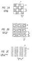
- Fig. 2 shows examples of arrangement of monocrystalline Al seeds.
- apertures of a lateral length of L1 are formed in a checkered pattern in an insulation film 11, formed for example on a Si surface, and monocrystalline Al is selectively deposited in said apertures.
- An unrepresented non-monocrystalline A1 film is formed on the insulation film 11 and on the monocrystalline Al in the apertures 12, and is converted into monocrystalline state by heating, utilizing the monocrystalline Al as the seeds.
- apertures of a lateral length L2 are formed as via hole pattern with an interval L3, and, in an example in Fig.
- a line-and-space pattern is formed by insulators 11 of a width L5 and apertures 12 of a width L4.
- the monocrystalline Al is deposited selectively in the apertures, and an unrepresented non-monocrystalline Al film is formed, covering the monocrystalline Al and the insulator.
- the non-monocrystalline Al film is converted into monocrystalline state, utilizing the monocrystalline Al as the seeds.
- the basic procedure consists of preparing a specimen of a cross section as shown in Fig. 1A or 1B, and subjecting said specimen to ion implantation followed by heating. Observations were made with X-ray diffraction, conventional RHEED and scanning ⁇ -RHEED microscope, before and after the heating.
- the transition of the second Al from the polycrystalline state to the monocrystalline state by heating is ascribed to the rearrangement of Al atoms, based on the increased flowability thereof. It is already known that a semiconductor containing a covalent bonding such as Si or GaAs present on a thin insulation film can be converted into monocrystalline state by heating.
- an Al or Al-Si film, present on an insulation film can be grown into polycrystals consisting of crystal grains of several microns by a heat treatment of 450°C, but the present invention is based on a finding that Al or Al-Si present on an insulator can be converted into monocrystalline state over an area in excess of 10 ⁇ m if a monocrystalline Al area is present under such Al or Al-Si film.
- Heating of the specimen can be achieved, for example, by heating in an electric oven with an atmosphere of H 2 , N 2 or Ar or a mixture thereof, heating in vacuum, heating with a rapid thermal annealer (RTA), heating with a laser, heating with a linear heater such as a carbon heater, high frequency heating, lamp heating or electron beam heating.
- RTA rapid thermal annealer
- a pure Al film or an Al-Si film formed on Si reacts, when heated, with Si thereby causing erosion of the Si substrate or a leak in the Si pn junction present below the Al or Al-Si film.
- the heating treatment should preferably be conducted at a temperature as low as possible.
- the Al atoms have to become flowable by thermal energy. Consequently the heating method is preferably such as to heat the Al or Al-Si alone but not the Si substrate present thereunder.
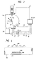
- Heating in vacuum can be achieved, in a scanning ⁇ -RHEED microscope shown in Fig. 3, by a heater positioned behind the substrate.
- FIG. 3 there are shown an electron gun 20; an electron beam 21; a diffracted electron beam 22; a fluorescent plate 23; optical fibers 24, 24', 24"; photomultipliers 25, 25', 25"; diffraction spot intensity signals 26, 26', 26” converted into electrical signals; a scanning signal 27; a cathode ray tube (CRT) 28; a secondary electron signal 29; a secondary electron detector 30; a specimen 31; a vacuum chamber 34; and a vacuum system 35.
- CTR cathode ray tube
- a specimen as shown in Fig. 1A is placed in the vacuum chamber 34, and is heated from the back by a heater 32.
- the temperature of the specimen is measured from the back thereof by a thermocouple 33.
- the heating may also be conducted by a lamp or a laser instead of the heater.
- RTA rapid thermal annealer
- the RTA can heat solely the wafer surface within a short period, thereby minimizing the reaction of Al or Al-Si with the Si substrate.
- Fig. 4 shows an example of the RTA.
- a substrate 200 is supported by fingers 205 of a quartz substrate support 201.
- a quartz tube 202 may have a circular or square cross section, or may be replaced by a metal tube, such as a stainless steel tube, equipped with a quartz window.
- a linear lamp 203 of which light is reflected by a reflector 204 and irradiates the specimen 200 whose Al deposition face is directed to said lamp, may be composed of a halogen lamp, tungsten lamp, a Xe lamp or a Xe-Hg lamp. In the present example there is employed a halogen lamp of a higher heating speed.
- the internal atmosphere can be H 2 , N 2 or Ar, or a mixture thereof.
- the H 2 atmosphere is most preferred because highly pure gas, low in contents of moisture and oxygen, is available.
- the substrate temperature was measured at the surface thereof, by means of a radiation thermometer utilizing PbS as a detector.
- Laser heating can also heat the substrate surface only, and has an advantage of providing a wider monocrystalline area than with the RTA.
- the laser employable for this purpose can be an argon ion laser (hereinafter represented as Ar laser), a krypton ion laser (hereinafter represented as Kr laser), a He-Ne laser, a CO 2 laser, a YAG laser, an excimer laser such as ArF, KrF, XeF or XeCl laser with an output of several to twenty watts.
- the oscillation frequency can be continuous oscillation or pulsed oscillation of ca. 10 - 100 Hz.
- the laser heating is featured by a fact that the monocrystalline area can be enlarged by scanning of the specimen with the laser beam. Such enlargement of the monocrystalline area by laser scanning will be explained in the following.
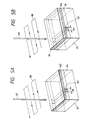
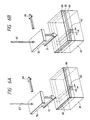
- Said specimen is scanned with a laser beam 67 in reciprocating manner as indicated by a line 68 in Fig. 5A, 5B or 7A, or in one direction as indicated by a line 69 in Fig. 6A, 6B or 7B.
- the laser beam is obtained from a continuously oscillated Ar laser or a pulse oscillated XeCl excimer laser and is focused to about 20 - 100 ⁇ m.
- a laser beam of a circular cross section is converted into a parallel beam 71 by an optical system 70 employing a cylindrical lens.
- the scanning direction of such laser beam or parallel laser beam is substantially perpendicular to the line of the first Al 62, as shown in Fig. 5A, 5B, 6A, 6B, 7A or 7B.
- a thermally oxidized SiO 2 layer of a thickness of ca. 7000 ⁇ (10 ⁇ 1 nm) is formed on the Si substrate, with a line width L10 of ca. 10 ⁇ m for the first Al 62 and with a thickness of ca. 5000 ⁇ for the second Al 63, the beam from an Ar laser is converted into a parallel beam 71 and the specimen is scanned in one direction 69 with a speed of ca. 1 cm/sec. The rear face of the specimen is not heated.
- the Ar laser has an output of ca. 20 - 50 W, with a power density of ca. 50 - 200 Kw/cm 2 on the specimen.
- the atmosphere of laser heating is H 2 gas of 1 atmosphere.
- the substrate temperature is measured at the position of irradiation, with a radiation thermometer employing a PbS detector.
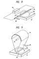
- Fig. 8 illustrates the method of heating with a linear heater.
- the substrate 82 to be heated is placed on a substrate support 81, made of carbon.
- a linear heater 83 which is also of carbon and energized by a power source 84.
- the substrate support 81 is also heated by a heater (not shown) provided at the bottom side of said support.
- the linear heater 83 moves in a direction 85.
- the atmosphere at heating may assume any pressure from vacuum to atmospheric pressure, and is preferably composed of H 2 , N 2 Ar or a mixture thereof in order to prevent the oxidation of Al surface. Single crystal formation is possible also in vacuum, but the structure of the apparatus is simpler when the atmospheric pressure is employed.
- the substrate temperature is measured with a radiation thermometer employing a PbS detector.
- the feature of heating with such linear heater lies, as in the laser heating, in a fact that the area of monocrystalline transformation can be expanded by scanning the heated area.
- Fig. 9 illustrates the heating method with a lamp, wherein a substrate 92 to be heated is placed on a substrate support 91, made of carbon.
- a lamp 93 can be a mercury lamp, a Hg-Xe lamp, a Xe lamp or a Xe flash lamp, and preferably has a linear structure.
- the light from the lamp 93 is condensed by a reflector 94 so as to form a line on the substrate surface.
- the substrate support 91 is also heated by a heater (not shown) provided on the bottom side thereof.
- the heated area 95 moves on the substrate in a direction 96, by the movement of the lamp.
- the atmosphere at heating may assume any pressure from atmospheric pressure to vacuum, and is preferably composed of H 2 , N 2 , Ar or a mixture thereof, in order to prevent oxidation of the Al surface.
- the single crystal formation is possible also in vacuum, but the atmospheric pressure allows to employ a simpler structure of the apparatus.
- the substrate temperature is measured by a radiation thermometer employing a PbS detector.
- Fig. 10 illustrates the heating method by high frequency heating.
- a substrate 103 to be heated is placed on a substrate support 101, made of carbon. Quartz plates 102 are provided with a gap therebetween.
- the substrate support bearing the substrate thereon as shown in Fig. 10 is heated by a high frequency coil (not shown) positioned therearound. Since the quartz plates 102 are not heated by the high frequency, a part 104 of the substrate is heated to a highest temperature.
- the atmosphere at heating may assume any pressure from atmospheric pressure to vacuum, and is preferably composed of H 2 , N 2 , Ar or a mixture thereof, in order to prevent oxidation of the Al surface.
- the single crystal formation is also possible in vacuum, but the atmospheric pressure allows to simplify the structure of the apparatus.
- the pressure of the atmosphere is atmospheric pressure.
- the substrate temperature is measured with a radiation thermometer employing a PbS detector.
- Fig. 11 illustrates the heating method with an electron beam.
- An electron beam 113 from a filament 112 is focused in the form of a line on a substrate 111 to be heated, by means of a condensing coil 115, a scanning coil and deflecting plates 115'.
- a linear portion 114 is heated to a high temperature.
- the heated area 114 also moves on the wafer.
- the atmosphere of heating is preferably high vacuum in order to prevent oxidation of the Al surface.
- the transformation of Al to monocrystalline state takes place at a presure of ca. 10 -6 Torr or lower.
- the moving speed of the substrate is ca. 0.5 - 10 cm/min.
- the substrate surface temperature in the heated area is measured with a radiation thermometer employing a PbS detector.
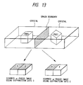
- the scanning ⁇ -RHEED microscope is disclosed in Extended Abstracts of the 21st Conference on Solid State Devices and Materials (1989) p.217 and Japanese Journal of Applied Physics Vol. 28, No. 11(1989) L2075.
- the conventional RHEED (reflection high energy electron diffraction) method is to irradiate the specimen surface with an electron beam at a shallow angle of 2 - 3° and to evaluate the crystallinity of the specimen surface from the diffraction pattern generated by the diffracted electron beam, but can only provide averaged information of the specimen surface, because the diameter of the electron beam is as large as 100 to several hundred ⁇ m.
- the diameter of the electron beam from the electron gun 20 is reduced to 0.1 ⁇ m, and the electron beam diffraction pattern from a specified small area on the specimen surface can be observed on the fluorescent plate 23. It is also possible to two-dimensionally scan the specimen surface with the electron beam 21, to guide the diffracted electron beam 22 to the fluorescent plate 23, to utilize the intensity change of an arbitrary diffraction spot on the diffraction pattern as image signals 26, 26', 26", and to obtain a two-dimensional image (scanning ⁇ -RHEED image) of the specimen surface by the diffraction spot intensity change on the CRT 28. In this method, observation of a scanning ⁇ -RHEED image employing different diffraction spots A, C on the diffraction pattern as shown in Fig.
- Said diffraction spot A is on a line l on which a plane of the diffraction spots and a sagittal plane of the incident electron beam perpendicularly cross, while the diffraction spot C is not on said line l.
- a plane of the diffraction spots and a sagittal plane of the incident electron beam perpendicularly cross are not on said line l.
- the scanning ⁇ -RHEED image utilizing the diffraction spot A shows both the crystal grains x, y as high intensity areas, but the image utilizing the spot C shows only the crystal grain x as the high intensity area. Consequently observation of the scanning ⁇ -RHEED image utilizing the diffraction spots A and C as shown in Fig. 12 allows to identify whether the crystal in the observed area is polycrystalline including in-plane rotation or monocrystalline.
- the preferred embodiment of the present invention utilizes monocrystalline Al formed in a via hole which is formed in an insulation film as a seed crystal, and converts non-monocrystalline Al in other areas into monocrystalline state by heating. It is preferable, after formation of monocrystalline Al by selective deposition of Al in the via hole, to non-selectively deposit Al also on the insulation film, and, after ion implantation, to apply heat treatment thereby converting Al on the insulation film into monocrystalline state. Such method allows to obtain a flat Al film, without formation of a recess in the Al film on the via hole.
- the non-monocrystalline Al film is once converted into amorphous or microcrystalline state, and is then transformed into monocrystalline state by heating, employing the monocrystalline Al as a seed crystal.
- the non-monocrystalline Al film formed as explained above, is subjected to the implantation of H + , Ar + , Si + or Al + ions by a known ion implanting method.
- H + , Ar + , Si + or Al + ions may also be employed, the above-mentioned four ions are preferably employed in order not to deteriorate the reliability of the Al or Al-Si wirings for ULSI, and Al + or H + ions are most preferable.
- Said H + , Al + , Ar + or Si + ions are preferably implanted with an acceleration voltage of ca. 50 kV or higher and with a dose of ca. 1 x 10 15 cm -2 or higher.
- the second Al can be converted into amorphous or microcrystalline state, even when said second Al has a thickness of ca. 5000 ⁇ .
- the ion implantation transforms Al, which is polycrystalline when deposited, into amorphous state. Since the Al atoms can more easily flow in the amorphous state than in the polycrystalline state, the transformation to monocrystalline state is achieved at a lower temperature than in the heat treatment at the polycrystalline state.
- a semiconductor having covalent bonds such as Si or GaAs on an insulating film is transformed into monocrystalline state by heat treatment.
- Si or GaAs on an insulating film is transformed into monocrystalline state by heat treatment.
- SPE single phase epitaxy
- silicon deposited on a monocrystalline Si substrate is converted into amorphous state by ion implantation, and is then converted to monocrystalline state by heat treatment for example in an electric oven.
- the present invention is based on a finding that even a metal film such as of Al present on an insulating film, after conversion into amorphous or microcrystalline state by ion implantation, can be transformed into monocrystalline state at a relatively low temperature. It is already known that an Al or Al-Si film on an insulating film can be grown into a polycrystalline film consisting of crystal grains of several microns by heat treatment of ca. 450°C. However transformation to the monocrystalline state by heat treatment has been impossible because the method of Al deposition for obtaining the structure shown in Fig. 1A has not been known, and also because the selectively deposited Al (first Al in Fig. 1A) has not been monocrystalline.
- the present invention has enabled, for the first time, to transform an Al film (second Al in Fig. 1A) on an insulating film into monocrystalline state by heat treatment after ion implantation, if selectively grown monocrystalline Al (first Al in Fig. 1A) is present thereunder.
- the semiconductor substrate is most preferably a Si substrate, but it may also be composed of GaAs, InP or Ge.
- the cross sectional structure of the specimen after formation of Al of Al-Si is as shown in Fig. 1A.
- an insulation film 5 may be present on the second Al film as shown in Fig. 1B.
- Said insulation film 5 may be composed of SiO 2 obtained by normal pressure CVD, phosphor-doped oxide film (PSG), boron-doped oxide film (BSG), phosphor- and boron-doped oxide film (BPSG), silicon nitride film (SiN) obtained by low pressure CVD, or silicon nitride film obtained by ECR.
- Specimens were prepared with monocrystalline seed patterns as explained before, namely a checkered pattern as shown in Fig. 2A with L1 within a range of 0.5 - 20 ⁇ m, or a via hole pattern as shown in Fig. 2B with L3 of 20 ⁇ m or less, or a line-and-space pattern with L5 of 20 ⁇ m, and also with non-monocrystalline Al on such monocrystalline seed pattern.
- X-ray diffraction and conventional RHEED observation proved the polycrystalline state, but were unable to identify the size of the crystal grains.
- Observation with a scanning ⁇ -RHEED microscope with an electron beam diameter reduced to 0.1 ⁇ m ⁇ provided a spot pattern shown in Fig. 14B though the intensity was weak.
- Fig. 15A shows the result of observation of the scanning ⁇ -RHEED image, utilizing the spot intensity variation on the diffraction pattern, wherein hatched areas indicate areas with a high diffraction spot intensity, while a white area indicates an area of weak intensity.
- the size of the hatched areas suggests that the size of the crystal grains is in the order of several to ten microns.
- Said specimen was implanted for example with Al + ions with an acceleration voltage of 50 kV and with a dose of 1 x 10 16 /cm 2 .
- Said ion implantation caused transformation of the second Al into amorphous or microcrystalline state. Said transformation was confirmed in the following manner.
- the X-ray diffraction showed a diffraction peak of Al(111) in the deposited state, but, after ion implantation, no longer showed diffraction peak for aluminum.
- observation of the electron beam diffraction pattern by the conventional RHEED apparatus did not show circular nor spot pattern but so-called hallow pattern, indicating that the Al or Al-Si film was transformed by the ion implantation into a state which is not monocrystalline nor polycrystalline but amorphous or microcrystalline.
- Fig. 14B The spots in Fig. 14B were identified as a diffraction pattern generated when the electron beam is introduced from a direction [101] into the Al(111) plane.
- Figs. 15B and 15C indicate the results of observation of the scanning ⁇ -RHEED image, utilizing the intensity of a spot A (111 diffracted spot) and a spot C (202 diffracted spot) on the diffraction pattern in Fig. 14B.
- monocrystalline Al can be formed on a substrate surface of any material.
- A1 wirings with preferred characteristics for use in semiconductor devices, such as surface properties, antimigration resistance, adhesion to the underlying silicon etc.
- the specimens used in the measurement having a cross-sectional structure as shown in Fig. 1A, were prepared in the following manner.
- a Si wafer was subjected to thermal oxidation at 1000°C by hydrogen combustion (H 2 : 4 1/min., O 2 : 2 l/min.).
- the surface orientation of Si wafer was (100) or (111).
- the entire wafer was coated with photoresist and was exposed to a desired pattern by an exposure apparatus. After the photoresist was developed, reactive ion etching was conducted, utilizing the photoresist as a mask, to etch the underlying SiO 2 , thereby locally exposing the Si surface.
- an Al film was deposited by a low pressure CVD method, employing dimethylaluminum hydride and hydrogen, with a deposition temperature of ca. 270°C and a pressure of ca. 1.5 Torr in the reactor tube.
- first A1 deposition was conducted solely on the exposed Si surface
- a surface modifying step was conducted by generating plasma in the low pressure CVD apparatus when the Al film thickness became equal to the SiO 2 film thickness, and Al (second Al) was deposited on the entire surface.
- SiO 2 films thickness was varied in 5 levels of 1000, 2500, 500, 7500 and 10000 ⁇ .
- the checkered pattern shown in Fig. 2A was used on the Si wafer, with size L1 varied in 8 levels of 0.25, 0.5, 1, 2, 3, 5, 10 and 20 pm.
- Thickness of the A1 film deposited on the entire surface was varied in 3 levels of 100, 2500 and 5000 ⁇ .
- the intensity was weak.
- the scanning ⁇ -RHEED image utilizing the diffracted spot intensity of the diffraction pattern provided an image as shown in Fig. 15A, wherein hatched areas indicate areas of high diffraction spot intensity, indicating polycrystalline state consisting of crystal grains of several to ten microns.
- the second Al was subjected to Al + implantation by known ion implanting method, with an acceleration voltage of 50 kV and a dose of 5 x 10 15 cm -2 or 1 x 10 16 cm -2 .
- the iron implanted specimens were heated treated in an electric over, at temperatures of 9 levels of 200°, 250°, 300°, 350°, 400°, 450°, 550° and 600°C, for about 3 hours, in hydrogen gas atmospheric pressure.
- the specimens were subjected to the observation of electron beam diffracted pattern and scanning ⁇ -RHEED image in the scanning ⁇ -RHEED microscope.
- Fig. 14B All the specimens treated at 250°C or higher showed spot patterns as shown in Fig. 14B, with higher intensities than before the heat treatment, regardless of the Si wafer surface orientation, SiO 2 film thickness, size of the checkered pattern or second Al film thickness.
- the diffraction pattern in Fig. 14B was identified, from the position of the diffracted spots, as being generated by the electron beam introduced from a direction [101] into the Al(111) plane.
- the scanning ⁇ -RHEED images, obtained utilizing the intensities of a diffracted spot A (111 diffracted spot) and a spot C (202 diffracted spot) on the diffraction pattern in Fig. 14B were similar to those shown in Figs.
- the second Al film which had been polycrystals when deposited by the LP-CVD method, was transformed into monocrystalline state by heat treatment, after transformation into amorphous state by ion implantation.
- the measurement of element distribution indicated diffusion of Si and Al at the interface of the insulation film on the substrate surface and the second Al film.
- Si + ion implantation was conducted with an acceleration voltage of 80 kV and a dose of 5 x 10 15 cm -2 or 1 x 10 16 cm -2 .
- the second Al was transformed by ion implantation into amorphous or microcrystalline state, and then to monocrystalline state at the heat treating temperature of 250°C or higher.
- the present example conducted implantation of H + ions in the same specimens and procedure as in the example G1.
- H + ion implantation was conducted with an acceleration voltage of 20 kV and a dose of 5 x 10 16 cm -2 or 1 x 10 17 cm -2 .
- the second Al was transformed by ion implantation into amorphous or microcrystalline state, and then to monocrystalline state at the heat treating temperature of 250°C or higher.
- the present example conducted implantation of Ar + ions in the same specimens and procedure as in the example G1.
- Ar + ion implantation was conducted with an acceleration voltage of 80 kV, and a dose of 5 x 10 16 cm -2 or 5 x 10 16 cm -2 .
- the second Al was transformed by ion implantation into amorphous or microcrystalline state, and then to monocrystalline state at the heat treating temperature of 250°C or higher.
- Specimens with a cross-sectional structure shown in Fig. 1A were prepared in the same manner as in the example G1, and were subjected to ion implantation and heat treatment.
- the via hole pattern shown in Fig. 2B was formed on the Si wafer, with size L2 varied in 5 levels of 0.25, 0.5, 1, 2 and 5 ⁇ m and size L3 varied in 5 levels of 1, 2, 5, 10 and 20 ⁇ m.
- size L2 varied in 5 levels of 0.25, 0.5, 1, 2 and 5 ⁇ m
- size L3 varied in 5 levels of 1, 2, 5, 10 and 20 ⁇ m.
- the thicknesses of the SiO 2 film and the Al film deposited on the entire wafer (second Al 4 in Fig. 1) were same as in the example G1.
- the specimens prepared as explained above were subjected to A1 + ion implantation in the same manner as in the example G1, then to heat treatment in the electric oven and subsequently observed.
- the A1 + ion implanting conditions and the heat treating conditions were same as in the example G1.
- the second Al in the deposited state by the LP-CVD method was identified, in any speciment, as polycrystals with an orientation (111), consisting of crystal grains of several to ten microns.
- the heat treatment in the electric oven was conducted in the same conditions as in the example G1, and the electron beam diffraction pattern and the scanning ⁇ -RHEED image were observed in the scanning ⁇ -RHEED microscope.
- the scanning ⁇ -RHEED images indicated, as in the example G1, that all the specimens treated at 250°C or higher were transformed into monocrystalline state, regardless of the surface orientation of the Si wafer, size of the checkered pattern or second Al film thickness.
- the measurement of element distribution in the direction of depth by Auger electron spectroscopy or secondary ion mass spectroscopy, indicated diffusion of Si and Al at the interface between the insulation film on the substrate surface and the second Al film when the substrate surface temperature was 600°C or higher.
- the present example conducted Si + ion implantation with the same specimens and procedure as in the example G5.
- Si + ion implanting conditions were same as those in the example G2.
- the present example conducted H + ion implantation with the same specimens and procedure as in the example G5.
- the present example conducted Ar + ion implantation with the same specimens and procedure as in the example G5.
- Specimens of a cross-sectional structure as shown in Fig. 1A were prepared in the same manner as in the example G1, and were subjected to ion implantation and heat treatment.
- the line-and-space pattern shown in Fig. 2C was formed on the Si wafer, with the size L4 varied in 5 levels of 0.25, 0.5, 1, 2 and 5 ⁇ m and size L5 in 5 levels of 1, 2, 5, 10 and 20 ⁇ m.
- 25 different line-and-space patterns were prepared by taking the combinations of L4 and L5.
- the thicknesses of the SiO 2 film and the Al deposited on the entire surface were same as in the example G1.
- the specimens prepared as explained above were subjected to Al + ion implantation in the same manner as in the example G1, then to heat treatment in the electric oven and were observed.
- the Al + ion implanting conditions and heat treating conditions were same as those in the example G1.
- the Al deposited on the entire surface (second Al) in any specimen was identified, as in the example G1, as polycrystals with an orientation (111), consisting of crystal grains of several to ten microns.
- the scanning ⁇ -RHEED image indicated, as in the example G1, that all the specimens treated at 250°C or higher were transformed to monocrystalline state regardless of the Si wafer surface orientation, SiO 2 film thickness, size of the checkered pattern or second Al film thickness. Also as in the example G1, the measurement of element distribution in the direction of depth, by Auger electron spectroscopy or secondary ion mass spectroscopy, indicated diffusion of Si and Al at the interface between the insulation film on the substrate surface and the second Al film, when the substrate surface temperature was 600°C or higher.
- the present example conducted Si + ion implantation with the same specimens and procedure as in the example G9.
- Si + ion implanting conditions were same as those in the example G3.
- the present example conducted H + ion implantation with the same specimens and procedure as in the example G9.
- the present example conducted Ar + ion implantation with the same specimens and procedure as in the example G9.
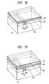
- the second Al was formed on the entire surface of the speciment, as shown in cross section in Fig. 1A.
- an insulation film was formed on the second Al of the specimens of the examples G1 - G12, as shown in Fig. 1B, and ion implantation and heat treatment with the electric oven were conducted in the same manner as in the examples G1 - G12.
- ion implantation and heat treatment with the electric oven were conducted in the same manner as in the examples G1 - G12.
- after the deposition of the first and second Al films there were conducted the ion implantation and then the heat treatment in the electric oven.
- the conditions of ion implantation and heat treatment were same as in the examples G1 - G12.
- the insulation film on the second Al film was composed of a SiO 2 film obtained by normal pressure CVD (hereinafter expressed as CVD-SiO 2 ), a boron-doped oxide film obtained by normal pressure CVD (BSG), a phosphor-doped oxide film obtained by normal pressure CVD (PSG), a boron- and phosphor-doped oxide film obtained by normal pressure CVD (BPSG), a nitride film obtained by plasma CVD (P-SiN), or a nitride film obtained by ECR apparatus (ECR-SiN).
- Said insulation film on the second Al will hereinafter be called the second insulation film.
- the thickness of the second insulation film was selected as 1000, 2000, 5000 or 10000 ⁇ .
- the heat treating temperature was same as in the examples G1 - G12. After the heat treatment, the second insulation film was removed by etching, and the electron beam diffraction pattern and the scanning ⁇ -RHEED image were observed, as in the examples G1 - G12, in the scanning ⁇ -RHEED microscope. There were obtained similar results to those in the examples G1 - G12, indicating that the second Al was transformed into monocrystalline state when the substrate temperature was 250°C or higher.
- the second Al film was formed on the entire surface of the specimen, as shown in cross section in Fig. 1A.
- an insulation film was formed on the second Al as shown in Fig. 1B, and ion implantation and heat treatment with the electric over were conducted in the same manner as in the examples G1 - G12.
- the present example conducted in succession the deposition of the first and second Al films, the deposition of the second insulation film, the ion implantation and the heat treatment with the electric oven.
- the conditions of ion implantation and heat treatment were same as in the examples G1 - G12.
- the insulation film on the second Al was composed of CVD-SiO 2 , BSG, PSG, BPSG, P-SiN or ECR-SiN, with a thickness of 500 or 1000 ⁇ .
- the heat treating temperature was same as in the examples G1 - G12.
- the second insulation film was removed by etching, and the electron beam diffraction pattern and the scanning ⁇ -RHEED image were observed, as in the examples G1 - G12, by the scanning ⁇ -RHEED microscope. There were obtained similar results to those in the examples G1 - G12, and the second Al was transformed to monocrystalline state when the substrate temperature was 250°C or higher.
- the first insulation film formed on the Si substrate was composed of SiO 2 formed by thermal oxidation.
- the insulation film on the Si substrate was composed of CVD-SiO 2 , BSG, PSG, BPSG, P-SiN, T-SiN, LP-SiN or ECR-SiN, with a thickness of 1000, 2500, 5000, 7500 or 10000 ⁇ .
- the thicknesses of the first and second Al films, and the ion implanting conditions were same as those in the examples G1 - G14.
- the second Al film was transformed into monocrystalline state when the substrate temperature was 250°C or higher. Also as in the examples G1 - G14, the measurement of element distribution in the direction of depth, by Auger electron spectroscopy or secondary ion mass spectroscopy, indicated diffusion of Si and Al at the interface between the insulation film on the substrate surface and the second Al film, when the substrate surface temperature was 600°C or higher.
- the insulation film on the Si substrate was provided with a gap of a width L10, in which monocrystalline Al (first Al) was formed. Said width was varied in 6 levels of 0.5, 1, 2, 5, 10 and 20 ⁇ m.
- the surface orientation of the Si wafer was selected as (100) or (111).
- the insulation film was composed of SiO 2 formed by thermal oxidation, with a thickness varied in 5 levels of 1000, 2500, 5000, 7500 and 10000 ⁇ .
- the second Al was identified, as in the example G1, as polycrystals consisting of crystal grains of several to ten microns.
- Al + ions were implanted under the same conditions as those in the example G1, whereby the second Al was transformed into amorphous or microcrystalline state. Thereafter heat treatment in the electric oven was conducted in the same conditions as in the example G1.
- Fig. 17A shows the pattern on the Si substrate, wherein the direction of first Al (line direction) is parallel to the y-direction in Fig. 17A.
- the length of the transformed monocrystalline area can be determined by measuring L8 in Fig. 17C.
- L8 is illustrated in the order of 10 - 20 ⁇ m in Fig. 17C, it was in fact about 1 cm when the substrate temperature was 250°C or higher.
- the second Al on SiO 2 was transformed into monocrystalline state over a length of 1 cm, utilizing monocrystalline first Al as the seed.
- the present example conducted Si + ion implantation with the same specimens and procedure as in the example G16.
- Si + ion implanting conditions were same as those in the example G2.
- the present example conducted H + ion implantation with the same specimens and procedure as in the example G16.
- the present example conducted Ar + ion implantation with same specimens and procedure as in the example G1.
- the second Al was formed on the entire surface of the specimen, as shown in Fig. 18.
- an insulation film was formed on the second Al film as shown in Fig. 19 and ion implantation and heat treatment with the electric oven were conducted in the same manner as in the examples G16 - G19.
- the deposition of the first and second Al films was followed by ion implantation and then heat treatment in the electric oven. The conditions of said ion implantation and heat treatment were same as in said examples G16 - G19.
- the insulation film (second insulation film) on the second Al film was composed of CVD-SiO 2 , BSG, PSG, BPSG, P-SiN or ECR-SiN, with a thickness of 1000, 2000, 5000 or 10000 ⁇ .
- the heat treating temperature was same as in the examples G16 - G19.
- the second insulation film was removed by etching, and the electron beam diffraction pattern and the scanning ⁇ -RHEED image were observed in the scanning ⁇ -RHEED microscope, as in the examples G16 - G19. There were obtained similar results to those in said examples, wherein the second Al was transformed into monocrystalline state with heat treatment at 250°C or higher.
- the second Al was formed on the entire surface of the specimen as shown in cross section in Fig. 1A.
- an insulation film was formed on the second Al in-the specimens of the examples G1 - G12, and ion implantation and heat treatment with the electric oven were conducted in the same manner as in the examples G16 - G19.
- the present example conducted, after the deposition of the first and second Al films, the deposition of the second insulation film, ion implantation and heat treatment by the electric oven.
- the conditions of ion implantation and heat treatment were same as in the examples G16 - G19.
- the insulation film on the second Al was composed of CVD-SiO 2 , BSG, PSG, BPSG, P-SiN or ECR-SiN, with a thickness of 500 or 1000 ⁇ .
- the heat treating temperature was same as in the examples G16 - G19.
- the second insulation film was removed by etching, and the electron beam diffraction pattern and the scanning ⁇ -RHEED were observed, as in the examples G16 - G19, in the scanning ⁇ -RHEED microscope. There were obtained similar results to those in the examples G16 - G19, wherein the second Al was transformed into monocrystalline state when the substrate temperature was 250°C or higher.
- the measurement of element distribution in the direction of depth, by Auger electron spectroscopy or secondary ion mass spectroscopy indicated diffusion of Si and Al at the interface between the insulation film on the substrate surface and the second Al film, when the substrate surface temperature was 600°C or higher.
- the first insulation film formed on the Si substrate of the structure shown in Fig. 18 or 19 was composed of SiO 2 obtained by thermal oxidation.
- the insulation film on the Si substrate was composed of CVD-SiO 2 , BSG, PSG, BPSG, P-SiN, T-Sin, LP-SiN, or ECR-SiN, with a thickness varied in 5 levels of 1000, 2500, 5000, 7500 and 10000 ⁇ .
- the thicknesses of the second Al film and of the second insulation film, and the ion implanting conditions, were same as those in the examples G16 - G21.
- the second Al was transformed into monocrystalline state when the substrate temperature was 250°C or higher. Also as in said examples, the measurement of element distribution in the direction of depth, by Auger electron spectroscopy or secondary ion mass spectroscopy, indicated diffusion of Si and Al at the interface between the insulation film on the substrate surface and the second Al film, when the substrate surface temperature was 600°C or higher.
- the first and second Al films were both composed of pure aluminum formed by a LP-CVD method employing DMAH (dimethylaluminum hydride) and hydrogen.
- pure aluminum was replaced by Al-Si, deposited by the addition of Si 2 H 6 in LP-CVD in addition to DMAH and hydrogen.
- the Si content in the first and second Al-Si films was selected as 0.2, 0.5 or 1.0%.
- the heat treatment was conducted in the same manner as in the examples G1 - G22, except that Al was replaced by Al-Si.
- the first and second Al films were both formed by the LP-CVD method employing DMAH and hydrogen.
- the first Al has to be monocrystalline.
- the LP-CVD method has the advantage of being capable of depositing the first and second Al films in succession in the same apparatus, but the second Al film need not be formed by CVD as long as it is polycrystalline or amorphous.
- the present example employed the same specimens and heat treating conditions as those in the examples G1 - G22, but the second Al film alone was formed by sputtering. Based on X-ray diffraction, electron beam diffraction pattern obtained by the conventional RHEED apparatus, and electron beam diffraction pattern and scanning ⁇ -RHEED image obtained by the scanning ⁇ -RHEED microscope, the second Al film in the deposited state was identified as polycrystals consisting of crystal grains of 1 ⁇ m or smaller.
- the first Al film was composed of Al-Si formed by LP-CVD employing DMAH, hydrogen and Si 2 H 6
- the second Al film was composed of pure aluminum formed by LP-CVD employing DMAH and hydrogen.
- the Si content in the first Al-Si film was selected as 0.2, 0.5 or 1.0 %.
- the first Al film was composed of Al-Si formed by LP-CVD employing DMAH, hydrogen and Si 2 H 6
- the second Al film was composed of Al-Si formed by sputtering.
- the Si content in the first Al-Si film was selected as 0.2, 0.5 or 1.0 %.
- the present invention can achieve transformation into monocrystalline state by a heat treatment, even in an Al film present on SiO 2 , if said SiO 2 is so patterned to expose a Si surface and monocrystalline Al is present on thus exposed Si surface.
- Said monocrystalline transformation can be achieved with heat treatment of a low temperature.
- Said transformed monocrystalline Al can be utilized in wirings and can improve the resistances to migration phenomena.
Landscapes
- Engineering & Computer Science (AREA)
- Microelectronics & Electronic Packaging (AREA)
- Condensed Matter Physics & Semiconductors (AREA)
- General Physics & Mathematics (AREA)
- Computer Hardware Design (AREA)
- Physics & Mathematics (AREA)
- Power Engineering (AREA)
- Manufacturing & Machinery (AREA)
- Internal Circuitry In Semiconductor Integrated Circuit Devices (AREA)
- Physical Vapour Deposition (AREA)
- Laminated Bodies (AREA)
- Inorganic Compounds Of Heavy Metals (AREA)
- Crystals, And After-Treatments Of Crystals (AREA)
- Electrodes Of Semiconductors (AREA)
Abstract
Description
Claims (8)
- A metal film forming method for a semiconductor device, comprising steps of:forming an insulation film (2) on a principal surface of a semiconductor substrate (1);forming an aperture in said insulation film (2) thereby exposing the surface of said semiconductor substrate (1);depositing a monocrystalline metal (3) composed of aluminum, selectively in said aperture, by a CVD method employing alkylaluminum hydride gas and hydrogen gas, so that a surface of said monocrystalline metal (3) is at the same level as the surface level of said insulation film (2);forming a metal film (4) principally composed of aluminum on said monocrystalline metal (3) and on said insulation film (2);converting said metal film by ion implantation to an amorphous state, a micro-crystalline state, or an amorphous state with microcrystalline inclusions; andheating said metal film (4) to 250°C or higher to convert at least a part thereof to monocrystalline state, utilising said monocrystalline metal (3) as a seed crystal.
- A method according to claim 1, wherein said heating is conducted after a second insulation film (5) is formed on said metal film (4).
- A method according to claim 2, wherein said metal film (4) is heated by resistance heating.
- A method according to claim 2, wherein said metal film (4) is heated by radiation.
- A method according to claim 2, wherein said metal film (4) is heated by laser beam.
- A method according to claim 2, wherein said metal film (4) is heated by electron beam.
- A method according to claim 2, wherein said metal film (4) is heated by induction.
- A method according to any preceding claim in which said metal film includes Si.
Applications Claiming Priority (4)
| Application Number | Priority Date | Filing Date | Title |
|---|---|---|---|
| JP177555/90 | 1990-07-06 | ||
| JP2177555A JP2763659B2 (en) | 1990-07-06 | 1990-07-06 | Metal thin film formation method |
| JP2177554A JP2763658B2 (en) | 1990-07-06 | 1990-07-06 | Metal thin film formation method |
| JP177554/90 | 1990-07-06 |
Publications (3)
| Publication Number | Publication Date |
|---|---|
| EP0465264A2 EP0465264A2 (en) | 1992-01-08 |
| EP0465264A3 EP0465264A3 (en) | 1992-08-05 |
| EP0465264B1 true EP0465264B1 (en) | 1998-12-09 |
Family
ID=26498066
Family Applications (1)
| Application Number | Title | Priority Date | Filing Date |
|---|---|---|---|
| EP91306118A Expired - Lifetime EP0465264B1 (en) | 1990-07-06 | 1991-07-05 | Metal film forming method |
Country Status (7)
| Country | Link |
|---|---|
| US (1) | US5208187A (en) |
| EP (1) | EP0465264B1 (en) |
| KR (1) | KR950005257B1 (en) |
| CN (1) | CN1056015C (en) |
| AT (1) | ATE174450T1 (en) |
| DE (1) | DE69130595T2 (en) |
| MY (1) | MY107855A (en) |
Cited By (1)
| Publication number | Priority date | Publication date | Assignee | Title |
|---|---|---|---|---|
| WO2018201951A1 (en) * | 2017-05-02 | 2018-11-08 | 王武生 | Method for producing monocrystal metal |
Families Citing this family (25)
| Publication number | Priority date | Publication date | Assignee | Title |
|---|---|---|---|---|
| PT95232B (en) * | 1989-09-09 | 1998-06-30 | Canon Kk | PRODUCTION PROCESS OF A DEPOSITED ALUMINUM FILM |
| EP0420597B1 (en) * | 1989-09-26 | 1996-04-24 | Canon Kabushiki Kaisha | Process for forming a deposited film by use of alkyl aluminum hydride and process for preparing semiconductor device |
| EP0498580A1 (en) * | 1991-02-04 | 1992-08-12 | Canon Kabushiki Kaisha | Method for depositing a metal film containing aluminium by use of alkylaluminium halide |
| JPH0521385A (en) * | 1991-07-10 | 1993-01-29 | Nippon Steel Corp | Manufacture of aluminium alloy thin film |
| JP3048749B2 (en) * | 1992-04-28 | 2000-06-05 | キヤノン株式会社 | Thin film formation method |
| US5288665A (en) * | 1992-08-12 | 1994-02-22 | Applied Materials, Inc. | Process for forming low resistance aluminum plug in via electrically connected to overlying patterned metal layer for integrated circuit structures |
| US6001461A (en) * | 1992-08-27 | 1999-12-14 | Kabushiki Kaisha Toshiba | Electronic parts and manufacturing method thereof |
| US5709958A (en) * | 1992-08-27 | 1998-01-20 | Kabushiki Kaisha Toshiba | Electronic parts |
| DE69333966T2 (en) * | 1992-08-27 | 2006-09-14 | Kabushiki Kaisha Toshiba, Kawasaki | Electronic component with metallic interconnects and method for its production |
| US5472911A (en) * | 1994-09-02 | 1995-12-05 | Motorola, Inc. | Method for controlling electromigration and electrically conductive interconnect structure therefor |
| JP3695606B2 (en) * | 1996-04-01 | 2005-09-14 | 忠弘 大見 | Semiconductor device and manufacturing method thereof |
| US5841179A (en) * | 1996-08-28 | 1998-11-24 | Advanced Micro Devices, Inc. | Conductive layer with anti-reflective surface portion |
| KR101027485B1 (en) * | 2001-02-12 | 2011-04-06 | 에이에스엠 아메리카, 인코포레이티드 | Improved process for deposition of semiconductor films |
| TW552645B (en) | 2001-08-03 | 2003-09-11 | Semiconductor Energy Lab | Laser irradiating device, laser irradiating method and manufacturing method of semiconductor device |
| US6847006B2 (en) * | 2001-08-10 | 2005-01-25 | Semiconductor Energy Laboratory Co., Ltd. | Laser annealing apparatus and semiconductor device manufacturing method |
| JP4397571B2 (en) | 2001-09-25 | 2010-01-13 | 株式会社半導体エネルギー研究所 | Laser irradiation method, laser irradiation apparatus, and manufacturing method of semiconductor device |
| US6750423B2 (en) | 2001-10-25 | 2004-06-15 | Semiconductor Energy Laboratory Co., Ltd. | Laser irradiation method, laser irradiation apparatus, and method of manufacturing a semiconductor device |
| JP2004303790A (en) * | 2003-03-28 | 2004-10-28 | Toshiba Corp | Semiconductor device |
| US6932865B2 (en) * | 2003-04-11 | 2005-08-23 | Lockheed Martin Corporation | System and method of making single-crystal structures through free-form fabrication techniques |
| CN101238095B (en) * | 2005-08-04 | 2011-08-10 | 东曹株式会社 | Metal-containing compound, method for producing the compound, metal-containing thin film and method for forming the thin film |
| US7732241B2 (en) | 2005-11-30 | 2010-06-08 | Semiconductor Energy Labortory Co., Ltd. | Microstructure and manufacturing method thereof and microelectromechanical system |
| US7485560B2 (en) * | 2006-11-22 | 2009-02-03 | Atomic Energy Council - Institute Of Nuclear Energy Research | Method for fabricating crystalline silicon thin films |
| JP5745205B2 (en) * | 2008-08-22 | 2015-07-08 | 木村 光照 | Thermal conductivity type barometric sensor using heating excitation |
| EP2322314A1 (en) * | 2009-11-16 | 2011-05-18 | Fraunhofer-Gesellschaft zur Förderung der angewandten Forschung e.V. | Monocrystalline welding of directionally fixed materials |
| US20210254237A1 (en) * | 2020-02-19 | 2021-08-19 | Jagannathan Rajagopalan | Synthesis of single crystal films on amorphous substrates |
Family Cites Families (8)
| Publication number | Priority date | Publication date | Assignee | Title |
|---|---|---|---|---|
| FR2571544B1 (en) * | 1984-10-05 | 1987-07-31 | Haond Michel | PROCESS FOR MANUFACTURING ELECTRICALLY ISOLATED MONOCRYSTALLINE SILICON ISLANDS FROM EACH OTHER |
| JPS62123716A (en) * | 1985-11-22 | 1987-06-05 | Nec Corp | Manufacture of semiconductor device |
| JPS62293740A (en) * | 1986-06-13 | 1987-12-21 | Fujitsu Ltd | Manufacture of semiconductor device |
| JP2735177B2 (en) * | 1986-08-18 | 1998-04-02 | 富士通株式会社 | Thin film transistor and method of manufacturing the same |
| JPH01109716A (en) * | 1987-10-22 | 1989-04-26 | Oki Electric Ind Co Ltd | Formation of contact in semiconductor device |
| JPH01120035A (en) * | 1987-11-02 | 1989-05-12 | Nec Corp | Semiconductor device and its manufacture |
| JPH01251740A (en) * | 1988-03-31 | 1989-10-06 | Seiko Epson Corp | Manufacture of semiconductor integrated circuit device |
| JP2726118B2 (en) * | 1989-09-26 | 1998-03-11 | キヤノン株式会社 | Deposition film formation method |
-
1991
- 1991-07-05 EP EP91306118A patent/EP0465264B1/en not_active Expired - Lifetime
- 1991-07-05 AT AT91306118T patent/ATE174450T1/en not_active IP Right Cessation
- 1991-07-05 DE DE69130595T patent/DE69130595T2/en not_active Expired - Lifetime
- 1991-07-05 MY MYPI91001220A patent/MY107855A/en unknown
- 1991-07-06 KR KR1019910011444A patent/KR950005257B1/en not_active IP Right Cessation
- 1991-07-06 CN CN91104047A patent/CN1056015C/en not_active Expired - Lifetime
- 1991-07-08 US US07/726,995 patent/US5208187A/en not_active Expired - Lifetime
Non-Patent Citations (5)
| Title |
|---|
| IBM Tech.Discl.Bull., vol. 15, no. 11, pp. 3525-26, April 1973. * |
| Ion Implantation and Beam Processing, J.S. Williams et al., Academic Press, 1984. * |
| Laser Annealing of Semiconductors, J.M. Poate et al., Academic Press, 1982. * |
| Material Science and Tech., R.W. Cahn et al., VCH, Germany, 1991. * |
| PAJ, vol. 13, no. 248 (E-770), 9/June/89. * |
Cited By (1)
| Publication number | Priority date | Publication date | Assignee | Title |
|---|---|---|---|---|
| WO2018201951A1 (en) * | 2017-05-02 | 2018-11-08 | 王武生 | Method for producing monocrystal metal |
Also Published As
| Publication number | Publication date |
|---|---|
| CN1056015C (en) | 2000-08-30 |
| CN1060558A (en) | 1992-04-22 |
| ATE174450T1 (en) | 1998-12-15 |
| DE69130595D1 (en) | 1999-01-21 |
| EP0465264A3 (en) | 1992-08-05 |
| DE69130595T2 (en) | 1999-05-27 |
| KR950005257B1 (en) | 1995-05-22 |
| MY107855A (en) | 1996-06-29 |
| US5208187A (en) | 1993-05-04 |
| EP0465264A2 (en) | 1992-01-08 |
Similar Documents
| Publication | Publication Date | Title |
|---|---|---|
| EP0465264B1 (en) | Metal film forming method | |
| EP0459772B1 (en) | Method of forming the wiring of a semiconductor circuit | |
| EP0425084B1 (en) | Process for forming deposited film by use of alkyl aluminum hydride | |
| US5580615A (en) | Method of forming a conductive film on an insulating region of a substrate | |
| US5482893A (en) | Method for producing semiconductor device having alignment mark | |
| US6355560B1 (en) | Low temperature integrated metallization process and apparatus | |
| EP0449524A2 (en) | Optical annealing method for semiconductor layer and method for producing semiconductor device employing the same semiconductor layer | |
| US4672740A (en) | Beam annealed silicide film on semiconductor substrate | |
| US5599741A (en) | Method for making semiconductor device with metal deposited on electron donating surface of gate electrode | |
| EP0434045B1 (en) | Method of forming conductive material selectively | |
| US4443493A (en) | Laser induced flow glass materials | |
| US6140229A (en) | Semiconductor apparatus and method of producing same | |
| EP0420597B1 (en) | Process for forming a deposited film by use of alkyl aluminum hydride and process for preparing semiconductor device | |
| EP0460857B1 (en) | Method for producing a semiconductor device with a high density wiring structure | |
| Pauleau | Chemical vapour deposition of tungsten films for metallization of integrated circuits | |
| KR100205301B1 (en) | Structure of interconnection and process for the same | |
| US4884120A (en) | Semiconductor device and method for making the same | |
| EP0084985A2 (en) | Laser induced flow Ge-O based materials | |
| JP2863277B2 (en) | Semiconductor device, manufacturing method thereof and alignment method | |
| JP2763658B2 (en) | Metal thin film formation method | |
| EP0459700B1 (en) | Wiring forming method for semiconducteur device | |
| JP2763659B2 (en) | Metal thin film formation method | |
| CA1249071A (en) | Direct writing of refractory metal lines for use in integrated circuit devices | |
| JPH0437029A (en) | Wiring forming method of semiconductor device | |
| KR100234397B1 (en) | Metal line forming method in silicon processing |
Legal Events
| Date | Code | Title | Description |
|---|---|---|---|
| PUAI | Public reference made under article 153(3) epc to a published international application that has entered the european phase |
Free format text: ORIGINAL CODE: 0009012 |
|
| AK | Designated contracting states |
Kind code of ref document: A2 Designated state(s): AT BE CH DE DK ES FR GB GR IT LI LU NL SE |
|
| PUAL | Search report despatched |
Free format text: ORIGINAL CODE: 0009013 |
|
| AK | Designated contracting states |
Kind code of ref document: A3 Designated state(s): AT BE CH DE DK ES FR GB GR IT LI LU NL SE |
|
| 17P | Request for examination filed |
Effective date: 19921221 |
|
| 17Q | First examination report despatched |
Effective date: 19940630 |
|
| GRAG | Despatch of communication of intention to grant |
Free format text: ORIGINAL CODE: EPIDOS AGRA |
|
| GRAG | Despatch of communication of intention to grant |
Free format text: ORIGINAL CODE: EPIDOS AGRA |
|
| GRAH | Despatch of communication of intention to grant a patent |
Free format text: ORIGINAL CODE: EPIDOS IGRA |
|
| GRAH | Despatch of communication of intention to grant a patent |
Free format text: ORIGINAL CODE: EPIDOS IGRA |
|
| GRAA | (expected) grant |
Free format text: ORIGINAL CODE: 0009210 |
|
| AK | Designated contracting states |
Kind code of ref document: B1 Designated state(s): AT BE CH DE DK ES FR GB GR IT LI LU NL SE |
|
| PG25 | Lapsed in a contracting state [announced via postgrant information from national office to epo] |
Ref country code: GR Free format text: LAPSE BECAUSE OF NON-PAYMENT OF DUE FEES Effective date: 19981209 Ref country code: ES Free format text: THE PATENT HAS BEEN ANNULLED BY A DECISION OF A NATIONAL AUTHORITY Effective date: 19981209 Ref country code: AT Free format text: LAPSE BECAUSE OF FAILURE TO SUBMIT A TRANSLATION OF THE DESCRIPTION OR TO PAY THE FEE WITHIN THE PRESCRIBED TIME-LIMIT Effective date: 19981209 Ref country code: CH Free format text: LAPSE BECAUSE OF FAILURE TO SUBMIT A TRANSLATION OF THE DESCRIPTION OR TO PAY THE FEE WITHIN THE PRESCRIBED TIME-LIMIT Effective date: 19981209 Ref country code: LI Free format text: LAPSE BECAUSE OF FAILURE TO SUBMIT A TRANSLATION OF THE DESCRIPTION OR TO PAY THE FEE WITHIN THE PRESCRIBED TIME-LIMIT Effective date: 19981209 Ref country code: NL Free format text: LAPSE BECAUSE OF FAILURE TO SUBMIT A TRANSLATION OF THE DESCRIPTION OR TO PAY THE FEE WITHIN THE PRESCRIBED TIME-LIMIT Effective date: 19981209 Ref country code: BE Free format text: LAPSE BECAUSE OF FAILURE TO SUBMIT A TRANSLATION OF THE DESCRIPTION OR TO PAY THE FEE WITHIN THE PRESCRIBED TIME-LIMIT Effective date: 19981209 |
|
| REF | Corresponds to: |
Ref document number: 174450 Country of ref document: AT Date of ref document: 19981215 Kind code of ref document: T |
|
| REG | Reference to a national code |
Ref country code: CH Ref legal event code: EP |
|
| REF | Corresponds to: |
Ref document number: 69130595 Country of ref document: DE Date of ref document: 19990121 |
|
| ET | Fr: translation filed | ||
| ITF | It: translation for a ep patent filed |
Owner name: SOCIETA' ITALIANA BREVETTI S.P.A. |
|
| PG25 | Lapsed in a contracting state [announced via postgrant information from national office to epo] |
Ref country code: DK Free format text: LAPSE BECAUSE OF FAILURE TO SUBMIT A TRANSLATION OF THE DESCRIPTION OR TO PAY THE FEE WITHIN THE PRESCRIBED TIME-LIMIT Effective date: 19990309 Ref country code: SE Free format text: LAPSE BECAUSE OF FAILURE TO SUBMIT A TRANSLATION OF THE DESCRIPTION OR TO PAY THE FEE WITHIN THE PRESCRIBED TIME-LIMIT Effective date: 19990309 |
|
| NLV1 | Nl: lapsed or annulled due to failure to fulfill the requirements of art. 29p and 29m of the patents act | ||
| REG | Reference to a national code |
Ref country code: CH Ref legal event code: PL |
|
| PG25 | Lapsed in a contracting state [announced via postgrant information from national office to epo] |
Ref country code: LU Free format text: LAPSE BECAUSE OF NON-PAYMENT OF DUE FEES Effective date: 19990705 |
|
| PLBE | No opposition filed within time limit |
Free format text: ORIGINAL CODE: 0009261 |
|
| STAA | Information on the status of an ep patent application or granted ep patent |
Free format text: STATUS: NO OPPOSITION FILED WITHIN TIME LIMIT |
|
| 26N | No opposition filed | ||
| REG | Reference to a national code |
Ref country code: GB Ref legal event code: IF02 |
|
| PGFP | Annual fee paid to national office [announced via postgrant information from national office to epo] |
Ref country code: FR Payment date: 20100806 Year of fee payment: 20 Ref country code: DE Payment date: 20100731 Year of fee payment: 20 Ref country code: IT Payment date: 20100719 Year of fee payment: 20 |
|
| PGFP | Annual fee paid to national office [announced via postgrant information from national office to epo] |
Ref country code: GB Payment date: 20100726 Year of fee payment: 20 |
|
| REG | Reference to a national code |
Ref country code: DE Ref legal event code: R071 Ref document number: 69130595 Country of ref document: DE |
|
| REG | Reference to a national code |
Ref country code: DE Ref legal event code: R071 Ref document number: 69130595 Country of ref document: DE |
|
| REG | Reference to a national code |
Ref country code: GB Ref legal event code: PE20 Expiry date: 20110704 |
|
| PG25 | Lapsed in a contracting state [announced via postgrant information from national office to epo] |
Ref country code: GB Free format text: LAPSE BECAUSE OF EXPIRATION OF PROTECTION Effective date: 20110704 |
|
| PG25 | Lapsed in a contracting state [announced via postgrant information from national office to epo] |
Ref country code: DE Free format text: LAPSE BECAUSE OF EXPIRATION OF PROTECTION Effective date: 20110706 |