EP0452793A2 - Optical head having a hologram associated with the objective lens - Google Patents
Optical head having a hologram associated with the objective lens Download PDFInfo
- Publication number
- EP0452793A2 EP0452793A2 EP91105688A EP91105688A EP0452793A2 EP 0452793 A2 EP0452793 A2 EP 0452793A2 EP 91105688 A EP91105688 A EP 91105688A EP 91105688 A EP91105688 A EP 91105688A EP 0452793 A2 EP0452793 A2 EP 0452793A2
- Authority
- EP
- European Patent Office
- Prior art keywords
- hologram
- optical
- imaging optics
- error signal
- diffraction
- Prior art date
- Legal status (The legal status is an assumption and is not a legal conclusion. Google has not performed a legal analysis and makes no representation as to the accuracy of the status listed.)
- Granted
Links
Images


Classifications
-
- G—PHYSICS
- G11—INFORMATION STORAGE
- G11B—INFORMATION STORAGE BASED ON RELATIVE MOVEMENT BETWEEN RECORD CARRIER AND TRANSDUCER
- G11B7/00—Recording or reproducing by optical means, e.g. recording using a thermal beam of optical radiation by modifying optical properties or the physical structure, reproducing using an optical beam at lower power by sensing optical properties; Record carriers therefor
- G11B7/12—Heads, e.g. forming of the optical beam spot or modulation of the optical beam
- G11B7/13—Optical detectors therefor
- G11B7/131—Arrangement of detectors in a multiple array
-
- G—PHYSICS
- G02—OPTICS
- G02B—OPTICAL ELEMENTS, SYSTEMS OR APPARATUS
- G02B27/00—Optical systems or apparatus not provided for by any of the groups G02B1/00 - G02B26/00, G02B30/00
- G02B27/0025—Optical systems or apparatus not provided for by any of the groups G02B1/00 - G02B26/00, G02B30/00 for optical correction, e.g. distorsion, aberration
- G02B27/0037—Optical systems or apparatus not provided for by any of the groups G02B1/00 - G02B26/00, G02B30/00 for optical correction, e.g. distorsion, aberration with diffracting elements
-
- G—PHYSICS
- G02—OPTICS
- G02B—OPTICAL ELEMENTS, SYSTEMS OR APPARATUS
- G02B27/00—Optical systems or apparatus not provided for by any of the groups G02B1/00 - G02B26/00, G02B30/00
- G02B27/42—Diffraction optics, i.e. systems including a diffractive element being designed for providing a diffractive effect
- G02B27/4233—Diffraction optics, i.e. systems including a diffractive element being designed for providing a diffractive effect having a diffractive element [DOE] contributing to a non-imaging application
- G02B27/4238—Diffraction optics, i.e. systems including a diffractive element being designed for providing a diffractive effect having a diffractive element [DOE] contributing to a non-imaging application in optical recording or readout devices
-
- G—PHYSICS
- G02—OPTICS
- G02B—OPTICAL ELEMENTS, SYSTEMS OR APPARATUS
- G02B27/00—Optical systems or apparatus not provided for by any of the groups G02B1/00 - G02B26/00, G02B30/00
- G02B27/42—Diffraction optics, i.e. systems including a diffractive element being designed for providing a diffractive effect
- G02B27/4272—Diffraction optics, i.e. systems including a diffractive element being designed for providing a diffractive effect having plural diffractive elements positioned sequentially along the optical path
- G02B27/4277—Diffraction optics, i.e. systems including a diffractive element being designed for providing a diffractive effect having plural diffractive elements positioned sequentially along the optical path being separated by an air space
-
- G—PHYSICS
- G02—OPTICS
- G02B—OPTICAL ELEMENTS, SYSTEMS OR APPARATUS
- G02B5/00—Optical elements other than lenses
- G02B5/18—Diffraction gratings
- G02B5/1814—Diffraction gratings structurally combined with one or more further optical elements, e.g. lenses, mirrors, prisms or other diffraction gratings
- G02B5/1819—Plural gratings positioned on the same surface, e.g. array of gratings
-
- G—PHYSICS
- G02—OPTICS
- G02B—OPTICAL ELEMENTS, SYSTEMS OR APPARATUS
- G02B5/00—Optical elements other than lenses
- G02B5/18—Diffraction gratings
- G02B5/1847—Manufacturing methods
- G02B5/1857—Manufacturing methods using exposure or etching means, e.g. holography, photolithography, exposure to electron or ion beams
-
- G—PHYSICS
- G02—OPTICS
- G02B—OPTICAL ELEMENTS, SYSTEMS OR APPARATUS
- G02B5/00—Optical elements other than lenses
- G02B5/32—Holograms used as optical elements
-
- G—PHYSICS
- G11—INFORMATION STORAGE
- G11B—INFORMATION STORAGE BASED ON RELATIVE MOVEMENT BETWEEN RECORD CARRIER AND TRANSDUCER
- G11B7/00—Recording or reproducing by optical means, e.g. recording using a thermal beam of optical radiation by modifying optical properties or the physical structure, reproducing using an optical beam at lower power by sensing optical properties; Record carriers therefor
- G11B7/08—Disposition or mounting of heads or light sources relatively to record carriers
- G11B7/09—Disposition or mounting of heads or light sources relatively to record carriers with provision for moving the light beam or focus plane for the purpose of maintaining alignment of the light beam relative to the record carrier during transducing operation, e.g. to compensate for surface irregularities of the latter or for track following
- G11B7/094—Methods and circuits for servo offset compensation
-
- G—PHYSICS
- G11—INFORMATION STORAGE
- G11B—INFORMATION STORAGE BASED ON RELATIVE MOVEMENT BETWEEN RECORD CARRIER AND TRANSDUCER
- G11B7/00—Recording or reproducing by optical means, e.g. recording using a thermal beam of optical radiation by modifying optical properties or the physical structure, reproducing using an optical beam at lower power by sensing optical properties; Record carriers therefor
- G11B7/12—Heads, e.g. forming of the optical beam spot or modulation of the optical beam
- G11B7/123—Integrated head arrangements, e.g. with source and detectors mounted on the same substrate
-
- G—PHYSICS
- G11—INFORMATION STORAGE
- G11B—INFORMATION STORAGE BASED ON RELATIVE MOVEMENT BETWEEN RECORD CARRIER AND TRANSDUCER
- G11B7/00—Recording or reproducing by optical means, e.g. recording using a thermal beam of optical radiation by modifying optical properties or the physical structure, reproducing using an optical beam at lower power by sensing optical properties; Record carriers therefor
- G11B7/12—Heads, e.g. forming of the optical beam spot or modulation of the optical beam
- G11B7/135—Means for guiding the beam from the source to the record carrier or from the record carrier to the detector
- G11B7/1353—Diffractive elements, e.g. holograms or gratings
-
- G—PHYSICS
- G11—INFORMATION STORAGE
- G11B—INFORMATION STORAGE BASED ON RELATIVE MOVEMENT BETWEEN RECORD CARRIER AND TRANSDUCER
- G11B7/00—Recording or reproducing by optical means, e.g. recording using a thermal beam of optical radiation by modifying optical properties or the physical structure, reproducing using an optical beam at lower power by sensing optical properties; Record carriers therefor
- G11B7/08—Disposition or mounting of heads or light sources relatively to record carriers
- G11B7/09—Disposition or mounting of heads or light sources relatively to record carriers with provision for moving the light beam or focus plane for the purpose of maintaining alignment of the light beam relative to the record carrier during transducing operation, e.g. to compensate for surface irregularities of the latter or for track following
- G11B7/0908—Disposition or mounting of heads or light sources relatively to record carriers with provision for moving the light beam or focus plane for the purpose of maintaining alignment of the light beam relative to the record carrier during transducing operation, e.g. to compensate for surface irregularities of the latter or for track following for focusing only
- G11B7/0912—Disposition or mounting of heads or light sources relatively to record carriers with provision for moving the light beam or focus plane for the purpose of maintaining alignment of the light beam relative to the record carrier during transducing operation, e.g. to compensate for surface irregularities of the latter or for track following for focusing only by push-pull method
Definitions
- the present invention relates to an optical head apparatus for recording and reproducing optical data recorded on an optical memory medium such as an optical disk, optical card and the like, a magnet-optic recording medium and the like.
- An optical memory technology which can develop a pit-shaped pattern in correspondence to signals in time series, has been practically used as a memory medium of high density and large capacity with the fields of application thereof extended from a digital audio disk to a data file.
- the optical memory technology starts from the development of a memory medium and is completed by the development of an optical head apparatus.
- the reduction in size and cost and the improvement of performance and reliability of the optical head apparatus is indispensable to the spread of the optical memory technology and an optical head apparatus having an integrated source and photodetecting system as well as integrated electronic circuits has been developed.
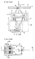
- Figures 1(a) and 1(b) show two examples of the optical system of a conventional integrated optical head apparatus.
- Figure 1(c) is a detailed view of the optical system shown in Figure 1(a), wherein the wavefront of divergent light from a source 100 using a semiconductor laser is divided into a main beam and two auxiliary beams at a first grating 101 and incident on a second grating 102 and a third grating 103 each having a semi-circular opening.
- a zero order diffracted wave component of the incident beam is focused on a memory medium 4 through a collimator 104 and an objective lens 105.
- the distance d' between the spots of the main beam 107a and auxiliary beams 107b, 107c is designed to about 10 to 20 micrometers.
- These beams are reflected or diffracted by the pit surface of the memory medium 4, passed again through the objective lens 105 and the collimator 104, diffracted by the second and third gratings each arranged as a partial pattern of a holographic element, and received by a photodetecting system 108 split into 5 regions, whereby a focus is detected by a Foucault method and a tracking and an RF signal are detected by a 3-beam method.
- the gratings 101, 102, and 103 which are formed on the opposite surfaces of the holographic element 109 can split the light into a plurality of wavefronts, and can be easily copied.
- the permissible fluctuation of a wavelength of the optical head apparatus is limited to about + 10 nm even if other assembly errors are zero.
- an optical head apparatus employing a spot size detection system (SSD) by which spots focused on two different focuses are differentially detected by linear photo-sensors interposed between the two focuses, as a focusing signal detection system which can allow a large amount of the relative positional error between a source 100 and a photodetecting system 3600 as shown in Figure 1(b).
- SSD spot size detection system
- this system obtains a tracking signal by differentially sensing a far field pattern of the tracking groove or pit in a memory medium 4, when a memory medium having only a pit train without having a groove, such as the so-called compact disk is reproduced, the tracking signal is unstably detected due to the offset of a servo signal caused by the inclination of the compact disk or the movement of an objective lens 3. Further, there remains a problem to realize a hologram element which can be easily blazed for restraining an unnecessary diffracted beam component as a hologram head arrangement for realizing a SSD system.
- the pattern of a third grating has a grating-shape having pitches of a few micrometers and further the pitches are set to 1 micrometer or less at the portion of the gratings where they intersect each other in order to make a distance h between the third grating and a source 100 to be a few millimeters, and thus the blazing thereof is very difficult.
- an object of the present invention is to provide an optical head apparatus wherein a large amount of the assembly error of a source and a photodetecting system is allowed when they are integrated, a stable servo signal with a restrained offset can be detected even from a memory medium having a shallow pit depth, and a diffraction optical element is provided which is easily blazed for restraining an unnecessary diffracted beam component. Further, another object of the present invention is to integrate an optical system as a whole to thereby further reduce the size of an optical head apparatus, lower the cost, and improve the mass-productivity and reliability thereof.
- bladezing gives a meaning of giving optical characteristics to an optical element such that photo-energy is concentrated to a specified diffraction component.
- An optical head apparatus comprises a light radiation source; an imaging optics or an objective lens for converging a light beam from the source to a micro-spot and causing the same to be incident upon a memory medium; and a hologram element including a blazed diffraction optical element upon which a light beam from the micro-spot on the memory medium is incident through the imaging optics, wherein a pair of Fresnel zone plate-like patterns, producing a plurality of diffraction wavefronts having a different focus from each other and the same diffraction order, outside of the optical-axis of the imaging optics, are formed in respective regions, having not superposed with each other that is, being separately from each other, a pair of blazed gratings separately formed in respective regions, a pair of photodetecting systems having a plurality of split regions for receiving beams from the diffraction wavefronts so as to differentially obtain a focusing error signal and a tracking error signal; and an actuator for controlling the imaging optics in response
- An optical head apparatus comprises a source; an imaging optics for converging a light beam from the source to a micro-spot and causing the same to be incident on a memory medium; and a diffraction optical element on which a light beam from the micro-spot on the memory medium is incident through the imaging optics, wherein a plurality of pairs of Fresnel zone plate-like patterns, which produce a plurality of diffraction wavefronts having different focuses from each other and the same diffraction order outside of the optical-axis of the imaging optics, are alternately disposed with the same width; a beam detection system having a focusing error signal detection unit for detecting the diffraction wavefronts formed by a pair of the Fresnel zone plate-like patterns and a tracking error detection unit for detecting the diffraction wavefronts produced in the direction in which pairs of the Fresnel zone plate-like patterns are alternately disposed with the same width; and an actuator for controlling the above imaging optics in response
- An optical head apparatus is arranged such that the above Fresnel zone plate-like patterns as stated in claim 1 or 2 are composed of linear Fresnel zone plate-like patterns formed in only a one-dimensional direction.
- An optical head apparatus is arranged such that the focusing detection unit and the tracking detection unit of the photodetector system as stated in claim 2 are disposed in parallel with the tracking direction of the memory means.
- a light beam from the source is focused into a micro-spot by the imaging optics and is then incident on the memory means, the light beam from the memory means is incident on a pair of the Fresnel zone plate-like patterns of the diffraction optical element through the imaging optics, and a pair of the diffraction beams are incident on a pair of the photodetecting systems outside the optical-axis of the imaging optics, so that the photodetecting systems output a data signal and differentially obtain a focusing error signal and a tracking error signal to drive the actuator.
- the light beam from the micro-spot focused on the above memory medium produces a pair of diffraction beams through the diffraction optical element, which are received by the respective split regions of a pair of the photodetecting systems to thereby differentially obtain the focusing error signal and the tracking error signal, a large amount of the relative positional error can be allowed between the source and the photodetecting systems as well as a detection can be stably carried out even from a memory medium having a shallow pit depth.
- the diffraction optical element is formed therein with a pair of the Fresnel zone plate-like patterns which are not superposed with each other, the occurrence of a beat beam which would be produced if they were superimposed can be prevented and the Fresnel zone plate-like patterns can be easily blazed, and thus unnecessary diffracted beam component can be restrained and the diffraction optical element can be integrally incorporated with the imaging optics in the vicinity thereof.
- the photodetecting systems has a focusing error signal detection unit for detecting diffraction wavefronts formed by a pair of the Fresnel zone plate-like patterns and a tracking error detection unit for detecting the diffraction wavefronts produced in the direction in which the pairs of the Fresnel zone plate-like patterns are alternately disposed with the same width, and thus the diffraction beam made by the pairs of the Fresnel zone plate-like patterns disposed with the same width are differentially detected by the tracking detection unit and a tracking error signal can be obtained by a 3-beam method.
- the detection surface of the detector systems has a beam cross section of a thin width in addition to the technical effects obtained by claim 1 or 2.
- the size in the pattern train direction of the linear Fresnel zone plate-like patterns can be reduced so that the size of the optical head apparatus can be reduced and the range of a response frequency can be easily increased and stable servo signals for tracking and focusing can be obtained even in a record erasing type optical disk and the like having a large fluctuation in wavelength of a source.
- the integral drive of the diffraction optical element and the imaging optics more stabilizes the serve detection since the offset is restrained.
- the focusing detection unit and the tracking detection unit of the photodetector system of claim 2 are disposed in parallel with the tracking direction of the memory means, a change in far field pattern, which is caused when the micro-spot of the focused light beam on the memory medium 4 goes across the tracking groove or pit train of the memory medium 4, does not affect the focusing error signal and thus a stable servo signal can be detected, in addition to the technical effects obtained by claim 2.
- the diffraction optical element 2 only uses a zero order diffracted beam on a going path and does not use a little defocused beam 9a and the like of a +1 order diffracted beam.
- a beam on a return pass reflected or diffracted from the pit surface 6 is incident upon the diffraction optical element 2 through the image optics 3 and produces the diffraction wavefronts 10, 11 of a plurality of beams 15, 16 having a different focus outside of an optical axis by the +1 order diffracted beam of the diffraction optical element 2.
- These diffraction wavefronts are incident upon a pair of the photodetecting systems 12, 13 in the vicinity of the focus of the +1 order diffracted beam.
- Designated at 8 is the drive unit of an actuator (not shown) having a movable unit 14 for integrally driving the focusing optics 3 and the diffraction optical element 2; designated at 35 is a holding unit for holding the source 1 and the photodetecting systems 12, 13; and X, Y and Z designate directions.
- each of the photodetecting systems 12, 13 has a plurality of split regions defined by slits, having a width of w and a length h in the split line direction.
- each photodetector uses a linear type silicon photodetector and fixed on the upper surface of the mount 17 of the source 1 and spaced apart from the beam radiation point 5 by a height g. Note that the height g can be arbitrarily set depending on the design of a Fresnel zone plate-like pattern.
- Designated at 610 to 612 are the output terminals of the respective split regions of the photodetecting system 12 and designated at 620 to 622 are the output terminals of the respective split regions of the photodetecting system 13.
- the diffraction wavefronts 10, 11 shown in Figure 11(a) have focuses to which beams reflected or diffracted by the pit surface 6 are converged, the focuses being located at positions apart from the beam receiving surface 36 of each of the photodetecting systems 12, 13 in the thicknesswise direction thereof by distances ⁇ 1, ⁇ 2, and when the focusing optics 3 focuses, the respective beams 15, 16 on the beam receiving surface 14 have the same beam size, but when the imaging optics 3 does not focuse the beam, the beam has a different size.
- This difference is detected as a differential signal after the photodetecting systems 12, 13 having carried out a photo-electric conversion and is fed back to the movable unit 14 of the actuator to thereby adjust the focus of the imaging optics 3.
- the above mentioned diffraction optical element 2 forms a Fresnel zone plate-like pattern on the side thereof facing to the phase-type hologram imaging optics 3, and is fixed to the movable unit of the actuator together with the imaging optics 3.
- the diffraction optical element 2 or the cylindrical unit 18 thereof is adjusted by being rotated about the beam radiation point 5 by a slight angle (arrows 19a, 19b) so that the positions of the beams 15, 16 are optimized with respect to the photodetecting systems 12, 13 shown in Figure 11(b) in such a manner as shown in the figure.
- l1 and l2 represent distances between the photodetecting systems 12, 13 and the beam radiation point 5
- ⁇ represents an angle at which a pair of the photodetecting systems 12, 13 are observed from the beam radiation point.
- Each of grating-like regions A, B is non-continously provided with linear Fresnel zone plate-like patterns disposed like a reed screen (off-axis linear Fresnel zone plates) so that they intersect at an angle ⁇ , and thus form blazed phase gratings having a cross section with a depth e as shown in Figure 12(b).
- each width Pj of regions A, B shown in Figure 12(a) is differently set to substantially restrain the formation of a primary order diffracted beam corresponding to a coarse grating cycle period.
- Figure 14(a) shows a design principle of the linear Fresnel zone plate-like patterns.
- the linear Fresnel zone plate-like patterns 20, 21 have centers at the points O1, O2 on a center line and a cross-sectional phase structure as shown in Figure 14(b), are given by the following relation which is similar to that known as a two-dimensional Fresnel ring band plate, and the pattern in the circle 22 surrounded by a dotted line of Figure 14(a) is used.
- r2 2j ⁇ fz + j2 ⁇ 2
- ⁇ represents the main wavelength of the source 1
- j represents a sequential number of a grating counted from the center O1, O2 of each Fresnel zone plate-like pattern
- fz represents a focal length (provided by the diffraction wavefront in one dimensional direction under the action of convex and concave lenses).
- the linear Fresnel zone plate-like patterns 20, 21 intersect to each other at an angle ⁇ .
- the grating regions A correspond to that obtained by drawing the half of the Fresnel zone plate-like pattern 20 of Figure 14(a), as observed through the reed screen having a width Pj
- the grating regions B correspond to that obtained by drawing the half of the Fresnel zone plate-like pattern 21, and they are not overlapped with each other.
- the distances L1, L2 between the center of the opening 22 and the axial centers 01, 02 of the linear zone pattern are given by the following equations, when the distances l1, l2 shown in Figures 11(a) and 11(b) and H (the distance between the diffraction optical element 2 and a detected surface 14) are given.
- a focusing error signal FE S610 - S620
- FE [S610 - (S611 + S612)] - [S620 - (S621 + S622)]
- TE (S611 - S612) + (S621 - S622)
- the actuator is driven so that the obtained focusing error signal and tracking error signal become zero.
- 31 designates the focused +1 order beam obtained in such a manner that the beam 9a of the +1 order beam on the going path is reflected on the pit surface 6 and then diffracted by the diffraction optical element 2 on the return path which however does not affect the photodetecting systems 12, 13; and 32 designates the focused zero order beam obtained in such a manner that the beam 9a of the +1 order beam on the going path is reflected on the pit surface 6 and then diffracted by the diffraction optical element 2 on the return path, which raises no problems at all.
- the arrangement is such that the beam coming from the micro spot after having been focused on the memory medium 4 produces a pair of diffracted beams through the diffraction optical element 2 and the diffracted beams are received by each split region of a pair of the photodetecting systems 12, 13 so that a tracking error signal and focusing error signal are differentially obtained, and thus a large degree of the relative positional error between the source 1 and the photodetecting systems 12, 13 can be allowed.
- a mechanical adjustment error can be allowed to 5 to 10 times as large as that of, for example, the astigmatic method (the tolerance in the case of the SSD method as compared with the astigmatic method was evaluated as the result of an experiment effected by the inventors).
- the diffraction optical element 2 is formed with a pair of the Fresnel zone plate-like patterns which are not superposed with each other, the occurrence of a beat beam which would be produced of they were superimposedly formed can be prevented and the Fresnel zone plate-like patterns can be easily blazed, resulting in that an unnecessary diffracted beam component can be restrained and the diffraction optical element 2 can be integrated in the vicinity of the imaging optics 3.
- a pair of the diffracted beams are received by split regions of a pair of the optical instrument systems and differentially detected, tracking and focusing stable servo signals can be detected even if a memory medium having a shallow pit depth is used.
- the Fresnel zone plate-like pattern is a linear Fresnel zone plate-like pattern formed only in the one dimentional direction and it gives a beam having a cross section of a micro width on the detecting surface of the photodetector, the size in the pattern train direction of the linear Fresnel zone plate-like pattern can be shortened. More specifically, the size of the photodetecting systems 12, 13 can be set as h ⁇ w, as shown Figure 11(b).
- the size of the mount 17 as the substrate on which the source 1 and the photodetecting systems 12, 13 are integrated can be reduced and the range of a response frequency can be easily increased, and thus, tracking and focusing stable servo signals can be detected, even with, for example, a record and erasing type optical disk and the like having a large fluctuation in wavelength of a source.
- the linearization of the Fresnel zone plate-like pattern enables the same to be more easily blazed and the serve detection is more stabilized by integrally driving the optical element 2 and the imaging optics 3.
- the source 1 may be a semi-coherent beam.
- the Fresnel zone plate-like pattern has a sawtooth-shaped cross section as shown in Figure 12(b), it may be blazed stepwise, as shown in Figure 14(c), to restrain the ratio of a -1 order diffracted beam to a +1 order diffracted beam.
- Figures 15(a) and 15(b) show a second embodiment according to the present invention. More specifically, this optical head apparatus is arranged in the first embodiment such that a plurality of each pair of the Fresnel zone plate-like patterns of the diffraction optical element 2 are alternately disposed with the same width. Further, a pair of photodetecting systems 29, 30 are composed of focusing detection units 37, 38 for detecting diffraction wavefronts 15, 16 produced by a pair of the Fresnel zone plate-like patterns and tracking detection units 39 to 42 for detecting diffraction wavefronts 25 to 28 which are produced in the disposing direction of the pairs of the Fresnel zone plate-like patterns which are alternately disposed with the same width p thereof.
- auxiliary beam made by a diffraction optical element 2 on a going path produces micro-spots at the focusing points 24a, 24b on a pit surface 6 and the reflected or diffracted beam thereof is diffracted by the diffraction optical element 20 thereby to produce auxiliary beams 25, 26 and 27, 28 on a return path.
- each of the photodetecting systems 29, 30 is split into three regions each having a rectangular opening and uses a differential type linear photodetector.
- the relationship between the tracking direction (pit train direction) X0 of the a memory medium 4 and the direction X in which the regions A, B of the diffraction optical element 2 are disposed is substantially parallel, and thus the position of the auxiliary beam is adjusted similarly to that in a tracking detection system of the so-called 3-beam method.
- the diffracted beams made by pairs of the Fresnel zone plate-like patterns disposed with the same width P are differentially detected by the tracking detection units 39 to 42 thereby to obtain the tracking error signal by the 3-beam method.
- the photodetecting systems 29, 30 can obtain a correct signal in the vicinity of the focus of the diffraction optical element 2, the distance md between the respective diffracted beams can be minimized, where m is designed to about 0.2 in terms of the coupling ratio of an imaging optics 3 and d is designed to about 10 to 15 micrometers in terms of the distance between the point 7 on the pit surface 6 and the focusing points 24a and 24b.
- the 3-beam tracking system which has been widely applied for, for example, the memory medium 4 such as a compact disk having a pit train depth of about ⁇ /5 to a disk medium having a groove, can be further developed, so that the effect of an abnormal tracking error signal caused by flaws on a disk can be restrained without sacrificing other characteristics by designing the spot spacing of main and auxiliary beams to 12 micrometer or less. Further, the reduction in the beam spacing can increase the width P of the Fresnel zone plate-like pattern, and thus the diffraction optical element 2 can be easily made.
- the focusing detection units 37, 38 and the tracking detection units 39 to 42 of the photodetecting systems 29, 30 are disposed in parallel with the tracking direction X0 of the memory medium 4, i.e., the split line direction Y of the diffraction optical element 29, 30 is made orthogonal to the tracking direction X0, a change in a far field pattern, which is caused when the micro-spot having focused a light beam on the memory medium 4 goes across the tracking groove or pit train of the memory medium 4, does not affect the focusing error signal, and thus a stable servo signal can be detected.
- the diffraction optical element of a hologram element using the conventional 3-beam method needs to form gratings on the front and the back surfaces thereof in order to achieve a desired object, thus object can be achieved only by a relief pattern formed on one surface in this embodiment, and thus this embodiment is excellent in mass-productivity and reliability.
- this embodiment is excellent in mass-productivity and reliability.
- the embodiment has a great effect.
- the embodiment has functional effects similar to those of the first embodiment.
- the diffraction optical element 2 may be designed as a reflecting type phase grating and further the grating may be blazed to a sawtooth shape in accordance with the first and second embodiments.
- a technology of blazing the diffraction optical element 2 which is common to the respective embodiments can be realized, for example, in such a manner that after rectangular waveform gratings have been formed on a quartz substrate as a photoresist pattern, asymmetric grating are formed by oblique ion beam etching or electron beam drawing.
- one of the diffracted beam components (-1 order beam) produced in the diffraction on the return path from the Fresnel zone plate-like pattern is a weak beam and thus even if a portion thereof is mixed on the photodetecting systems 12, 13, 29, 30 as a zero order beam on the return path, the intensity ratio thereof to the -1 order beam can be made to 15 to 20% or less and the effect thereof can be substantially ignored.
- Figure 2(a) exemplifies a recent case of the optical system of an optical head apparatus simplified by using a hologram (e.g., Japanese Unexamined Patent No. 64-62838).
- a hologram e.g., Japanese Unexamined Patent No. 64-62838.
- 1 designates a light radiation source such as a semiconductor laser and the like.
- a radiated beam 110 (laser beam) coming from the source 1 passes through the hologram 101, is incident on an objective lens 8, and focused on an optical memory medium 4.
- a light beam reflected on the optical memory medium 4 follows an original beam path in the reverse direction and is incident upon the hologram 101.
- a +1 order diffracted beam 121 produced from the hologram is incident on a photodetector 36.
- a servo signal and a data signal can be obtained by calculating an output from the photodetector 36.
- an objective lens 3 can be moved by an actuator independently from the hologram 101
- the emitted beam 110 on the hologram 101 is also moved. Therefore, the image of a +1 order diffracted beam on the photodetector 36 is also moved, whereby the servo signal is adversely affected
- the hologram 101 and the objective lens 3 are disposed keeping a predetermined relative position with respect to the actuator 100, even if the objective lens 3 is moved with respect to the actuator 100 to effect a tracking control, the beam reflected on the optical memory medium 4 is little moved on the hologram 101. Therefore, a signal obtained from the photodetector 36 is not deteriorated regardless of that the objective lens 3 is moved.
- the diffracted beam is reflected on the optical memory medium 4 and focused on the photodetector 36 by the objective lens 3.
- a +1 order diffracted beam that is produced on the beam path from the memory medium 4 (hereinafter, referred to as a return path), which goes to the photodetector 36 after being reflected on the optical memory medium 4, focused by the objective lens 3 and diffracted by the hologram 101, is used to obtain a signal
- a -1 order beam produced on the going path is incident upon the same position as that of the +1 order diffracted beam on the return path on the photodetector 36.
- Figure 2(b) shows this state.
- the -1 order diffracted beam 121 on the going path which has become the zero order diffracted beam 130 on the return path and the +1 order diffracted beam 121 on the return path of the zero order diffracted beam 120 on the going path are reflected on different positions on the optical memory medium 4, and thus they naturally have different data. Therefore, this optical system having the integrated lens and hologram has a problem in that the quality of a servo signal and data signal is deteriorated by the -1 order beam 121 on the going path.
- the present invntion comprises a light radiation source, the objective lens for receiving a radiated beam coming from the light radiation source and causing the same to be focused on an optical memory medium, a blazed hologram integrally supported by the support member of the objective lens, and a photodetector for producing an output b receiving a diffracted beam which is produced by the radiated beam reflected on the above optical memory medium and incident on the objective lens integrated with the above hologram, the output being produced in accordance with each diffracted beam or a beam quality obtained by splitting each diffracted beam into a plurality of diffracted beams.
- the integration of the blazed hologram with the objective lens in the present invention enables an emitted beam on a return path to be incident on a predetermined portion of the hologram regardless of that the objective lens is moved because it follows a tracking, the diffracted beam produced from the hologram does not move on the photodetector.
- the hologram is blazed, i.e., since the cross section of the hologram is made asymmetric, the diffraction efficiency of the -1 order diffracted beam is smaller than that of a +1 order diffracted beam, and thus a servo signal or data signal is less deteriorated by the -1 order diffracted beam on the going path. Therefore, the servo and data signals can be stably read.
- Figure 6(a) is a diagram of the conceptual arrangement according to the present invention, which shows a simplified arrangement of Figure 11(a).
- Designated at 1 is a light radiation source such as a semiconductor laser or the like.
- a radiated beam 110 (laser beam) coming from the source passes through a hologram 2, is incident on an objective lens 3, and focused on a optical memory medium 4.
- the beam reflected on the optical memory medium 4 follows an original beam path and is incident on the hologram 2.
- a +1 order diffracted beam 121 produced from the hologram 2 is incident on a photodetector 36.
- a servo signal and a data signal can be obtained by calculating an output from the photodetector 36.
- the present invention is characterized in that the hologram 2 is blazed and integrated with the objective lens 3.
- the effect that the diffraction efficiency of a -1 order diffracted beam is made smaller than that of a +1 order diffracted beam can be obtained by the blazing, which is described, for example, in "Blazing of Micro Fresnel Lens Made by Electron Beam Drawing” by Fujita, Nishihara, Koyama, Technical Report of The Institute of Electronics, Information and Communication Engineers, Vol. 82, No. 47, pp 49-55 (OQE 82 - 25), 1982 and the like.
- the present invention uses the blazing to restrain the beam quantity of a -1 order diffracted beam on a going path produced from a hologram, wherein the blazing controls the beam quantity of the diffracted beam component of a zero order beam, a +1 order diffracted beam and the like.
- Figure 6(b) shows an example of a blazed hologram 200 which is embodied as an analog type hologram having a sawtooth-shaped cross section.
- Figure 7 shows a graph of the relationship between ⁇ and a diffraction efficiency.
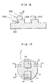
- Figs. 4(a) to 4(d) and Figs. 5(a) to 5(f) exemplify conventional methods of producing well-known blazed hologram.
- the blazed hologram is made in such a manner that, for example, as shown in Figures 4(a) to 4(d), a photoresist 3002 is coated on the surface of a substrate 300 shown in Figure 4(a), the photoresist is exposed after being covered with a chrome mask 3003 and then developed to make a masking pattern 3051, and further an ion beam 302 is obliquely irradiated to the surface of the substrate 300 shown in Figure 4(b) to obtain a blazed hologram 2001 as shown in Figure 4(c).
- Figure 5(d) is an enlarged view of a main part of Figure 5(c), wherein inclined surfaces A, B are asymmetrically formed.
- etching is repeated a plurality of times as shown in Figures 5(a) to 5(f), i.e., when a resist 3200 and a mask 3004 are formed and exposure in Figure 5(a) and development in Figure 5(b) are carried out after the process in Figure 5(c) has been carried out to form a masking pattern 3500, and then etching is carried out in this state, a blazed hologram 3082 having the surface thereof near to a sawtooth shape can be obtained, as shown in Figure 5(f).
- the cross section obtained by the method shown in Figures 4(a) to 4(d) is disadvantageous as shown in an enlarged view of Figure 4(d). More specifically, a surface A is not vertically formed but is inclined. Further, an inclined surface B has a concave shape.
- the conventional method has a problem in that since this method only provides a cross section which is different from the accurate sawtooth-shaped cross section shown in Figure 6(b), the intensity ratio of a conjugate diffracted beam cannot be sufficiently obtained. Further, since the blazed hologram 3082 of the conventional example shown in Figures 5(a) to 5(f) has a stepwise cross section, it is also a little difficult to increase the intensity ratio of the conjugate diffracted beam.
- a pattern alignment needs a very high accuracy of a few percents of grating pitches (e.g., about 2 micrometers when a grating has pitches of 10 micrometers) and thus a problem arises in that the manufacture thereof is more or less difficult.
- another object of the present invention is to provide a method of easily manufacturing a blazed hologram having a cross section near to an ideal sawtooth shape with a pinpoint accuracy. Further, an object of the present invention is to provide an optical head apparatus capable of detecting a signal having a good S/N ratio.
- a rectangular cross section is formed by etching, further a masking pattern is formed on a surface, and an ion beam is obliquely irradiated to form a blazed hologram. Further, an optical head apparatus is made using this hologram.
- a method according to the present invention comprises the steps of selectively forming a first masking pattern on a substrate and etching a portion of the substrate using the first masking pattern as a mask; and removing the first masking pattern, forming again a second masking pattern on the substrate, irradiating an ion beam to the surface of the substrate in a direction different from a right angle thereto to thereby selectively etching a portion of the substrate, and forming a sawtooth-shaped surface on the surface thereof.
- the present invention provides an optical head apparatus using the thus formed hologram.
- the present invention since the rectangular cross section is formed by etching and further an ion beam etching is obliquely carried out after the completion of the masking pattern, the accuracy of a pattern alignment is eased, and further since an amount of etching effected by the obliquely irradiated ion beam is small, a cross section nearer to a sawtooth shape can be obtained and thus a difference of the diffraction efficiency of a conjugate diffracted beam can be increased. Then, the present invention can realize an optical head apparatus capable of detecting a signal having a good S/N ratio.
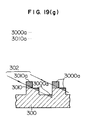
- a rectangular cross section 3001 shown in Figure 19(c) is made on the surface of a substrate 300 by etching using a masking pattern 3051, and then, as shown in Figures 19(d) and 19(e), a masking pattern 3010 is formed again by a resist using a chrome mask 4000 and a beam l2, an ion beam 302 is obliquely irradiated to etch the surface of the substrate 300 to thereby form a blazed hologram 2 having a sawtooth-shaped cross section shown in Figure 19(f).
- Figure 19(g) shows a process by which the saw-shaped cross section is formed by the obliquely irradiated ion beam 302.
- Figure 19(g) is an enlarged diagram of Figures 19(a) to 19(f).
- the portions 300a of the substrate 300 is etched by the obliquely irradiated ion beam 302.
- the portion 3010a to be etched of the masking pattern 3010 is etched, the portion 3000a to be etched of the substrate is increased and finally the sawtooth-shaped cross section shown in Figure 19(f) can be obtained.
- the masking pattern 301 even if the masking pattern 301 projects from the left edge of the convex portion 306 of the substrate 300 to the left side by d1, the masking pattern 301 does not prevent the formation of the rectangular cross section because it is etched by the ion beam 302.
- the masking pattern 3010 may be rather positively widened to make the left side of the convex perpendicular.
- the masking pattern even if the masking pattern projects from the center line L1 of the convex portion 306 to the right side by d2, the masking pattern also does not hinder the formation of the sawtooth-shaped cross section because the substrate 300 begins to be etched after the projected portion has been etched.
- the aligning accuracy of the chrome mask 4000 in the exposure in Figure 19(d) can be eased.
- the sawtooth can be made to a predetermined height [h in Figure 19(f)] in any portion of the split regions H1 to H4 in such a manner that pitches P1, P2, P3, and P4 in a certain direction (X direction) are made substantially the same as shown in Figure 17 and when the direction of the incident ion beam 302 is represented by a vector as shown in Figure 19(e), the direction of the obliquely projected vector to the two surfaces of the blazed hologram 2 is caused to coincide with the X direction.
- the reason thereof will be described below.
- making h constant enables the phase modulation amplitude of all the split regions (H1 to H4) to be constant, whereby the diffraction efficiency of all the split regions (H1 to H4) is made to be constant. Therefore, it is possible to make the diffraction efficiency of a +1 order diffracted beam substantially 100% in all the split regions (H1 to H4). Further, since the cross section of the hologram made by the manufacturing method of the present invention is very near to a sawtooth shape, it is very easy to increase zero and -1 order diffraction efficiencies and to reduce a -1 order diffraction efficiency.
- the hologram When the hologram is applied to an embodiment of a beam such as an optical pick-up apparatus shown in Figure 6(b) and the like, the utilization efficiency of the beam is improved and a stray beam produced on a going path by the diffraction made from the blazed hologram 2 can be reduced.
- the blazed hologram having the cross section near to a sawtooth shape enables a difference between the diffraction efficiencies of conjugate diffracted beams to be made larger. Further, an optical head apparatus capable of detecting a signal having a good S/N ratio can be produced by using the blazed hologram.
- E E z x E+1 (1)
- E z and E+1 represent the zero and +1 order diffraction efficiencies, respectively. Therefore, E z and E+1 need to be as large as possible to increase the utilization efficiency of a beam for the purpose of improving the S/N ratio of various signals, and thus it is found that the blazed hologram described above in the present invention must be used.
- the -1 order diffracted beam 121 is also produced on the going path, and the beam of the -1 order beam on the return path which has been reflected by the optical memory medium 4 and transmitted on the hologram 2 is incident on the photodetector 36 as a stray beam. Since the strah beam lowers the S/N ratio of a detected signal, the diffraction efficiency of the -1 order diffracted beam must be made as small as possible. For this purpose, it is found that the blazed hologram described above in the present invention is effective.
- Figure 8 shows an example analyzing the ratio of the beam quantity of the above stray beam and the signal beam.
- Table 1 shows the range of tolerance of a mechanical assembly error obtained by a computer simulation by comparing the hologram head (Type H-3) (SSD/slit detection method) shown in Figure 1(b) with the system of the embodiment of the present invention shown in Figure 6(c) (Type H-4).
- an assembly error as the tolerance was determined when a TE signal has a sensitivity lowered to 90% of an maximum value and an offset was 10% of a maximum value. It is found from Table 1 that the latter exhibits a tolerance which is greater than 2 times as large that of the former.
- Figure 10 explains a method of determining the center of a fringe pattern when the holographic element by the SDD method according to the present invention is designed by a computer and shows the positional relationship of the points (x, y, z) of the surface 2 of the hologram element, a reference source R (O, O, O), and an object point O1 (x1, y1, z1), O2 (x2, y2, z2).
- a hologram pattern having a trapezoidal opening as shown in Figure 18(b) can be synthesized by a computer to an optical head apparatus using a reflection type hologram element 2000 shown in Figure 18(a) as another embodiment of the present invention.
- the embodiment of the present invention shown in Figure 18(a) is an optical system simpler than an integrated optical system constituting the SSD system using a micro prism 999 shown in Figure 3 (Japanese Patent Unexamined No. 1-118224 filed by Sony) and further has a higher freedom of design.
- the optical head apparatus of this embodiment is different from the previous embodiment in that not only a laser source 100 is integrated with a photodetector 36 but also the entire optical system is fixed on the optical-axis of a lens 333 for integration.
- the conditions, under which the off-axis aberration of the asperical lens 333 is caused are restrained to thereby realize the micro objective lens 333 having a short conjugate length, and thus the entire optical system can be easily accommodated in an actuator.
- an asperical lens having a conjugate length of 10 mm could be realized with the weight of the entire optical system including a lens barrel of 1 g.
- a hologram element 2000 shown in Figure 18(b) explains that the opening in the reflection hologram used in the arrangement in Figure 18(a) is vertically asymmetric and optimized.
- the method of designing the hologram element in this case is similar to that of a transmission type one, except that the hologram surface (x, y, z) thereof is inclined by about 45° with respect to an optical-axis z.
Abstract
Description
- The present invention relates to an optical head apparatus for recording and reproducing optical data recorded on an optical memory medium such as an optical disk, optical card and the like, a magnet-optic recording medium and the like.
- An optical memory technology, which can develop a pit-shaped pattern in correspondence to signals in time series, has been practically used as a memory medium of high density and large capacity with the fields of application thereof extended from a digital audio disk to a data file.
- The optical memory technology starts from the development of a memory medium and is completed by the development of an optical head apparatus. In particular, the reduction in size and cost and the improvement of performance and reliability of the optical head apparatus is indispensable to the spread of the optical memory technology and an optical head apparatus having an integrated source and photodetecting system as well as integrated electronic circuits has been developed.
- Figures 1(a) and 1(b) show two examples of the optical system of a conventional integrated optical head apparatus. Figure 1(c) is a detailed view of the optical system shown in Figure 1(a), wherein the wavefront of divergent light from a
source 100 using a semiconductor laser is divided into a main beam and two auxiliary beams at afirst grating 101 and incident on asecond grating 102 and athird grating 103 each having a semi-circular opening. A zero order diffracted wave component of the incident beam is focused on amemory medium 4 through acollimator 104 and anobjective lens 105. Here, the distance d' between the spots of themain beam 107a andauxiliary beams memory medium 4, passed again through theobjective lens 105 and thecollimator 104, diffracted by the second and third gratings each arranged as a partial pattern of a holographic element, and received by a photodetectingsystem 108 split into 5 regions, whereby a focus is detected by a Foucault method and a tracking and an RF signal are detected by a 3-beam method. Note that thegratings holographic element 109 can split the light into a plurality of wavefronts, and can be easily copied. - However, when a semiconductor laser is used as a source, in the optical head apparatus, the permissible fluctuation of a wavelength of the optical head apparatus is limited to about + 10 nm even if other assembly errors are zero. Further, the tolerance of the relative positional error between the
source 100 and the photodetectingsystem 108 is set to ΔX ≅ 17 micrometers in the X-axial direction and ΔY ≅ 40 micrometers in the Y axial direction in the example shown in Figure 1 for the reduction in size and the integration of the optical head apparatus, supposing that the objective lens has the focus length f = 4.5 mm and the numerical aperture NA = 0.45, and the collimator lens has the focus length f = 21 mm and the numerical aperture N = 0.11, and thus the assembly must be carried out with a pinpoint accuracy in a manufacturing process. In particular, in the case of an optical disk drive device provided with a recording/erasing system, it is difficult to ensure the reliability thereof in the circumference in which the device is used. This is because that a conventional Foucault method or astigmatic method is used as a focusing servo signal sensing system for the optical head apparatus, that is, this is because of the restriction resulting from the system (Foucault method) for forming a micro-spot (~ 10 micrometer dia.) on the surface of the photo-sensor or the system (astigmatism method) for sensing the balance of a distributed light quantity on the surface of a photo-sensor split into four sections. Whereas, there has been developed an optical head apparatus employing a spot size detection system (SSD) by which spots focused on two different focuses are differentially detected by linear photo-sensors interposed between the two focuses, as a focusing signal detection system which can allow a large amount of the relative positional error between asource 100 and a photodetectingsystem 3600 as shown in Figure 1(b). (USP No. 4,929,823). - However, since this system obtains a tracking signal by differentially sensing a far field pattern of the tracking groove or pit in a
memory medium 4, when a memory medium having only a pit train without having a groove, such as the so-called compact disk is reproduced, the tracking signal is unstably detected due to the offset of a servo signal caused by the inclination of the compact disk or the movement of anobjective lens 3. Further, there remains a problem to realize a hologram element which can be easily blazed for restraining an unnecessary diffracted beam component as a hologram head arrangement for realizing a SSD system. In the arrangement shown in Figure 1(b), the pattern of a third grating has a grating-shape having pitches of a few micrometers and further the pitches are set to 1 micrometer or less at the portion of the gratings where they intersect each other in order to make a distance h between the third grating and asource 100 to be a few millimeters, and thus the blazing thereof is very difficult. - Therefore, an object of the present invention is to provide an optical head apparatus wherein a large amount of the assembly error of a source and a photodetecting system is allowed when they are integrated, a stable servo signal with a restrained offset can be detected even from a memory medium having a shallow pit depth, and a diffraction optical element is provided which is easily blazed for restraining an unnecessary diffracted beam component. Further, another object of the present invention is to integrate an optical system as a whole to thereby further reduce the size of an optical head apparatus, lower the cost, and improve the mass-productivity and reliability thereof.
- Here, a definition should be made, that is, the term "blazing" gives a meaning of giving optical characteristics to an optical element such that photo-energy is concentrated to a specified diffraction component.
- An optical head apparatus according to
claim 1 comprises a light radiation source; an imaging optics or an objective lens for converging a light beam from the source to a micro-spot and causing the same to be incident upon a memory medium; and a hologram element including a blazed diffraction optical element upon which a light beam from the micro-spot on the memory medium is incident through the imaging optics, wherein a pair of Fresnel zone plate-like patterns, producing a plurality of diffraction wavefronts having a different focus from each other and the same diffraction order, outside of the optical-axis of the imaging optics, are formed in respective regions, having not superposed with each other that is, being separately from each other, a pair of blazed gratings separately formed in respective regions, a pair of photodetecting systems having a plurality of split regions for receiving beams from the diffraction wavefronts so as to differentially obtain a focusing error signal and a tracking error signal; and an actuator for controlling the imaging optics in response to signals from the photodetecting systems so that the micro-spot scans the memory medium, and the above imaging optics or objective lens and the above hologram element are integrally supported and can be driven in response to a servo signal. - An optical head apparatus according to
claim 2 comprises a source; an imaging optics for converging a light beam from the source to a micro-spot and causing the same to be incident on a memory medium; and a diffraction optical element on which a light beam from the micro-spot on the memory medium is incident through the imaging optics, wherein a plurality of pairs of Fresnel zone plate-like patterns, which produce a plurality of diffraction wavefronts having different focuses from each other and the same diffraction order outside of the optical-axis of the imaging optics, are alternately disposed with the same width; a beam detection system having a focusing error signal detection unit for detecting the diffraction wavefronts formed by a pair of the Fresnel zone plate-like patterns and a tracking error detection unit for detecting the diffraction wavefronts produced in the direction in which pairs of the Fresnel zone plate-like patterns are alternately disposed with the same width; and an actuator for controlling the above imaging optics in response to signals from the photodetecting systems so that the micro-spot scans the memory medium. - An optical head apparatus according to
claim 3 is arranged such that the above Fresnel zone plate-like patterns as stated inclaim - An optical head apparatus according to
claim 4 is arranged such that the focusing detection unit and the tracking detection unit of the photodetector system as stated inclaim 2 are disposed in parallel with the tracking direction of the memory means. - According to the optical head apparatus of
claim 1, a light beam from the source is focused into a micro-spot by the imaging optics and is then incident on the memory means, the light beam from the memory means is incident on a pair of the Fresnel zone plate-like patterns of the diffraction optical element through the imaging optics, and a pair of the diffraction beams are incident on a pair of the photodetecting systems outside the optical-axis of the imaging optics, so that the photodetecting systems output a data signal and differentially obtain a focusing error signal and a tracking error signal to drive the actuator. - In this case, since the light beam from the micro-spot focused on the above memory medium produces a pair of diffraction beams through the diffraction optical element, which are received by the respective split regions of a pair of the photodetecting systems to thereby differentially obtain the focusing error signal and the tracking error signal, a large amount of the relative positional error can be allowed between the source and the photodetecting systems as well as a detection can be stably carried out even from a memory medium having a shallow pit depth. Further, since the diffraction optical element is formed therein with a pair of the Fresnel zone plate-like patterns which are not superposed with each other, the occurrence of a beat beam which would be produced if they were superimposed can be prevented and the Fresnel zone plate-like patterns can be easily blazed, and thus unnecessary diffracted beam component can be restrained and the diffraction optical element can be integrally incorporated with the imaging optics in the vicinity thereof.
- According to the optical head apparatus of
claim 2, a plurality of pairs of the Fresnel zone plate-like patterns of the diffraction optical element are alternately disposed and the photodetecting systems has a focusing error signal detection unit for detecting diffraction wavefronts formed by a pair of the Fresnel zone plate-like patterns and a tracking error detection unit for detecting the diffraction wavefronts produced in the direction in which the pairs of the Fresnel zone plate-like patterns are alternately disposed with the same width, and thus the diffraction beam made by the pairs of the Fresnel zone plate-like patterns disposed with the same width are differentially detected by the tracking detection unit and a tracking error signal can be obtained by a 3-beam method. In this case, since it is sufficient that the photodetecting systems can obtain a correct signal in the vicinity of the focus of the diffraction optical element, the distance between the respective diffraction beams can be minimized and the intervals of the Fresnel zone plate-like patterns can be increased, so that the diffraction optical element can be easily made. Other functions ofclaim 2 are the same as those ofclaim 1. - According to the optical head apparatus of
claim 3, since the above Fresnel zone plate-like patterns ofclaim claim - According to the optical head apparatus of
claim 4, since the focusing detection unit and the tracking detection unit of the photodetector system ofclaim 2 are disposed in parallel with the tracking direction of the memory means, a change in far field pattern, which is caused when the micro-spot of the focused light beam on thememory medium 4 goes across the tracking groove or pit train of thememory medium 4, does not affect the focusing error signal and thus a stable servo signal can be detected, in addition to the technical effects obtained byclaim 2. -
- Figures 1(a) and 1(b) are perspective views respectively illustrating examples of optical systems of conventional optical head apparatuses;
- Figure 1(c) is a perspective view illustrating details of the optical system shown in Figure 1(a);
- Figures 2(a) and 2(b) are schematic views illustrating a conventional optical head apparatus and showing optical paths in a conventional optical head apparatus;
- Figure 3 is a sectional view illustrating the optical head apparatus shown in Figure 2(a);
- Figures 4(a) to 5(f) are sectional views showing conventional processes of manufacturing optical diffraction elements;
- Figure 6(a) is a conceptional view illustrating an arrangement according to the present invention;
- Figure 6(b) is a cross-sectional view illustrating a part of an optical diffraction element used in the arrangement shown in Figure 6(a);
- Figure 6(c) is a sectional view illustrating the arrangement shown in Figure 6(a);
- Figure 7 is a graph showing a relationship between a phase modulation degree and a diffraction efficiency;
- Figures 8(a) and 8(b) are views illustrating a result of analysis, in one example form, concerning the beam quantity ratio between stray beam and signal beam;
- Figure 9 is a graph showing an example of measured servo characteristics of a SSD system shown in Figure 6(c);
- Figure 10 is a perspective view illustrating an optical system for determining a fringe pattern on the optical diffraction element;
- Figure 11(a) is a schematic view illustrating a first embodiment of an optical head apparatus according to the present invention;
- Figure 11(b) is a plan view illustrating a mount on which a beam source and photodetecting systems of the optical head apparatus shown in Figure 11(a) are incorporated;
- Figure 12(a) is a plan view illustrating an optical diffraction element having a blazed hologram which is essential in the first embodiment of the present invention;
- Figure 12(b) is a cross-sectional view illustrating the diffraction element shown in Figure 12(a);
- Figure 13 is a plan view showing a mask pattern for fabricating a diffraction element;
- Figure 14(a) is a view showing a basic design of linear Fresnel zone plate-like patterns;
- Figure 14(b) is a cross-sectional view illustrating a phase structure giving the linear Fresnel zone plate-like patterns shown in Figure 14(a);
- Figure 14(c) is a cross-sectional view illustrating a phase structure variant from the structure shown in Figure 14(b);
- Figure 15(a) is a perspective view illustrating a second embodiment of the optical head apparatus according to the present invention;
- Figure 15(b) is a plan view illustrating a mount on which a beam source and photodetecting system of the optical head apparatus shown in Figure 15(b) are provided;
- Figure 16 is an enlarged sectional view illustrating a part of a diffraction element according to the present invention;
- Figure 17 is a plan view illustrating an example of the optical diffraction element having a blazed hologram;
- Figure 18(a) is a sectional view illustrating the other embodiment of an optical head apparatus according to the present invention;
- Figure 18(b) is a plan view illustrating a hologram pattern used in the optical head apparatus shown in Figure 18(a); and
- Figures 19(a) to 19(g) are sectional views showing a process of manufacturing an optical diffraction element according to the present invention.
- A first embodiment according to the present invention will be described below with reference to Figure 11(a). More specifically, in Figure 11(a), designated at 1 is a source using a semiconductor laser producing a coherent beam having a wavelength in a near infrared rays region (e.g., λ = 780 nm); designated at 2 is a diffraction optical element using a hologram element in which Fresnel zone plate-like patterns are formed being not overlapped with each other for producing a plurality of diffraction wavefronts having the same diffraction order and different focuses outside the optical-axis; designated at 3 is an image optics using an objective lens having a numerical aperture NA = about 0.45; designated at 4 is a memory medium such as a compact disk, optical disk having a tracking groove or the like; and designated at 12 and 13 are a pair of photodetecting systems having a plurality of split regions for respectively receiving the above diffraction wavefronts and differentially obtaining a focusing error signal and a tracking error signal.
- A beam radiated from the
beam radiation point 5 of thesource 1 onto the diffractionoptical element 2, is converged to a micro-spot at theimage optics 3, and is incident upon a focusingpoint 7 on the pit surface 6 of thememory medium 4. At this time, the diffractionoptical element 2 only uses a zero order diffracted beam on a going path and does not use a littledefocused beam 9a and the like of a +1 order diffracted beam. In addition, a beam on a return pass reflected or diffracted from the pit surface 6 is incident upon the diffractionoptical element 2 through theimage optics 3 and produces thediffraction wavefronts 10, 11 of a plurality ofbeams optical element 2. These diffraction wavefronts are incident upon a pair of thephotodetecting systems - Designated at 8 is the drive unit of an actuator (not shown) having a
movable unit 14 for integrally driving the focusingoptics 3 and the diffractionoptical element 2; designated at 35 is a holding unit for holding thesource 1 and thephotodetecting systems - In Figure 11(b), each of the
photodetecting systems mount 17 of thesource 1 and spaced apart from thebeam radiation point 5 by a height g. Note that the height g can be arbitrarily set depending on the design of a Fresnel zone plate-like pattern. Designated at 610 to 612 are the output terminals of the respective split regions of thephotodetecting system 12 and designated at 620 to 622 are the output terminals of the respective split regions of thephotodetecting system 13. The diffraction wavefronts 10, 11 shown in Figure 11(a) have focuses to which beams reflected or diffracted by the pit surface 6 are converged, the focuses being located at positions apart from thebeam receiving surface 36 of each of thephotodetecting systems optics 3 focuses, therespective beams beam receiving surface 14 have the same beam size, but when theimaging optics 3 does not focuse the beam, the beam has a different size. This difference is detected as a differential signal after thephotodetecting systems movable unit 14 of the actuator to thereby adjust the focus of theimaging optics 3. - Further, the above mentioned diffraction
optical element 2 forms a Fresnel zone plate-like pattern on the side thereof facing to the phase-typehologram imaging optics 3, and is fixed to the movable unit of the actuator together with theimaging optics 3. Before fixed thereto, the diffractionoptical element 2 or the cylindrical unit 18 thereof is adjusted by being rotated about thebeam radiation point 5 by a slight angle (arrows 19a, 19b) so that the positions of thebeams photodetecting systems photodetecting systems beam radiation point 5, and ϑ represents an angle at which a pair of thephotodetecting systems - Figure 12(a) is a conceptual view of the diffraction
optical element 2 wherein two kinds of coarse grating regions A, B each having a width Pj (= P1 ~ Pn) are alternately disposed. Each of grating-like regions A, B is non-continously provided with linear Fresnel zone plate-like patterns disposed like a reed screen (off-axis linear Fresnel zone plates) so that they intersect at an angle ϑ, and thus form blazed phase gratings having a cross section with a depth e as shown in Figure 12(b). Further, each width Pj of regions A, B shown in Figure 12(a) is differently set to substantially restrain the formation of a primary order diffracted beam corresponding to a coarse grating cycle period. - Figure 14(a) shows a design principle of the linear Fresnel zone plate-like patterns. The linear Fresnel zone plate-
like patterns circle 22 surrounded by a dotted line of Figure 14(a) is used.

where, λ represents the main wavelength of thesource 1, j represents a sequential number of a grating counted from the center O₁, O₂ of each Fresnel zone plate-like pattern, and fz represents a focal length (provided by the diffraction wavefront in one dimensional direction under the action of convex and concave lenses). These patterns can achieve the object thereof by being recorded by a laser interference fringe or being formed by a computer which calculates the patterns. - Further, the linear Fresnel zone plate-
like patterns like pattern 20 of Figure 14(a), as observed through the reed screen having a width Pj, the grating regions B correspond to that obtained by drawing the half of the Fresnel zone plate-like pattern 21, and they are not overlapped with each other. Here, the distances L₁, L₂ between the center of theopening 22 and theaxial centers 0₁, 0₂ of the linear zone pattern are given by the following equations, when the distances ℓ₁, ℓ₂ shown in Figures 11(a) and 11(b) and H (the distance between the diffractionoptical element 2 and a detected surface 14) are given.


where, fz₁ and fz₂ represent the focal distances of a pair of the Fresnel zone plate-like patterns - When output signals from the
output terminals 610 to 612 and 620 to 622 of thephotodetecting systems

Alternately, when a beam utilization efficiency is more improved, it is given by:

Further, in this embodiment, the tracking direction of thememory medium 4 is caused to coincide with the direction Y of the split line of thephotodetecting systems

- In addition, an RF signal is given by:

or

- Then, the actuator is driven so that the obtained focusing error signal and tracking error signal become zero.
- Note that in Figure 11(b), 31 designates the focused +1 order beam obtained in such a manner that the
beam 9a of the +1 order beam on the going path is reflected on the pit surface 6 and then diffracted by the diffractionoptical element 2 on the return path which however does not affect thephotodetecting systems beam 9a of the +1 order beam on the going path is reflected on the pit surface 6 and then diffracted by the diffractionoptical element 2 on the return path, which raises no problems at all. - According to the embodiment, the arrangement is such that the beam coming from the micro spot after having been focused on the
memory medium 4 produces a pair of diffracted beams through the diffractionoptical element 2 and the diffracted beams are received by each split region of a pair of thephotodetecting systems source 1 and thephotodetecting systems - Further, since the diffraction
optical element 2 is formed with a pair of the Fresnel zone plate-like patterns which are not superposed with each other, the occurrence of a beat beam which would be produced of they were superimposedly formed can be prevented and the Fresnel zone plate-like patterns can be easily blazed, resulting in that an unnecessary diffracted beam component can be restrained and the diffractionoptical element 2 can be integrated in the vicinity of theimaging optics 3. Moreover, a pair of the diffracted beams are received by split regions of a pair of the optical instrument systems and differentially detected, tracking and focusing stable servo signals can be detected even if a memory medium having a shallow pit depth is used. - Further, since the Fresnel zone plate-like pattern is a linear Fresnel zone plate-like pattern formed only in the one dimentional direction and it gives a beam having a cross section of a micro width on the detecting surface of the photodetector, the size in the pattern train direction of the linear Fresnel zone plate-like pattern can be shortened. More specifically, the size of the
photodetecting systems mount 17 as the substrate on which thesource 1 and thephotodetecting systems optical element 2 and theimaging optics 3. - Note that the detail of a two-dimensional Fresnel zone pattern will be apparent from, for example, Japanese Unexamined Patent Nos. 62-251025 and 62-251026.
- The
source 1 may be a semi-coherent beam. - Further, although the Fresnel zone plate-like pattern has a sawtooth-shaped cross section as shown in Figure 12(b), it may be blazed stepwise, as shown in Figure 14(c), to restrain the ratio of a -1 order diffracted beam to a +1 order diffracted beam. As a design example of Figure 14(c), level differences between 4 stages can be made equal to each other so as to realize such conditions as a depth e ≒ 870 nm, a refractive index of an element substrate n ≒ 1.455, a wavelength λ = 788 nm, a beam utilization efficiency in the going and return paths


- Figures 15(a) and 15(b) show a second embodiment according to the present invention. More specifically, this optical head apparatus is arranged in the first embodiment such that a plurality of each pair of the Fresnel zone plate-like patterns of the diffraction
optical element 2 are alternately disposed with the same width. Further, a pair ofphotodetecting systems 29, 30 are composed of focusingdetection units 37, 38 for detectingdiffraction wavefronts detection units 39 to 42 for detectingdiffraction wavefronts 25 to 28 which are produced in the disposing direction of the pairs of the Fresnel zone plate-like patterns which are alternately disposed with the same width p thereof. - More specifically, when all of the widths Pj of the grating-like regions A, B shown in Figure 12(a) are set to have the same value Pj ≡ P, a new primary order diffracted beam corresponding to the grating cycle periods having a width P is produced as an auxiliary beam. The auxiliary beam made by a diffraction
optical element 2 on a going path produces micro-spots at the focusingpoints 24a, 24b on a pit surface 6 and the reflected or diffracted beam thereof is diffracted by the diffractionoptical element 20 thereby to produceauxiliary beams diffraction wavefronts auxiliary beams 25 to 28. In Figure 15(b), each of thephotodetecting systems 29, 30 is split into three regions each having a rectangular opening and uses a differential type linear photodetector. Theoutput terminals photodetectors 37, 38 and theoutput terminals photodetectors 39 to 42 deliver output signals S81, S82, S91, and S92, and accordingly, a focusing error signal FE and a tracking error signal TE are given by:


- Further, the relationship between the tracking direction (pit train direction) X₀ of the a
memory medium 4 and the direction X in which the regions A, B of the diffractionoptical element 2 are disposed is substantially parallel, and thus the position of the auxiliary beam is adjusted similarly to that in a tracking detection system of the so-called 3-beam method. - Note that designated at 33, 34 are the centers of +1 order diffracted beams obtained in such a manner that the +1 diffracted beams of the auxiliary beam, which are made by the diffraction
optical element 2 on the going path and focused on the focusingpoints 24a, 24b, are reflected on thememory medium 4 and are then diffracted by the diffractionoptical element 2. - According to the embodiment, the diffracted beams made by pairs of the Fresnel zone plate-like patterns disposed with the same width P are differentially detected by the tracking
detection units 39 to 42 thereby to obtain the tracking error signal by the 3-beam method. In this case, it is sufficient that if thephotodetecting systems 29, 30 can obtain a correct signal in the vicinity of the focus of the diffractionoptical element 2, the distance md between the respective diffracted beams can be minimized, where m is designed to about 0.2 in terms of the coupling ratio of animaging optics 3 and d is designed to about 10 to 15 micrometers in terms of the distance between thepoint 7 on the pit surface 6 and the focusingpoints 24a and 24b. Therefore, the 3-beam tracking system, which has been widely applied for, for example, thememory medium 4 such as a compact disk having a pit train depth of about λ/5 to a disk medium having a groove, can be further developed, so that the effect of an abnormal tracking error signal caused by flaws on a disk can be restrained without sacrificing other characteristics by designing the spot spacing of main and auxiliary beams to 12 micrometer or less. Further, the reduction in the beam spacing can increase the width P of the Fresnel zone plate-like pattern, and thus the diffractionoptical element 2 can be easily made. - In addition, since the focusing
detection units 37, 38 and the trackingdetection units 39 to 42 of thephotodetecting systems 29, 30 are disposed in parallel with the tracking direction X₀ of thememory medium 4, i.e., the split line direction Y of the diffractionoptical element 29, 30 is made orthogonal to the tracking direction X₀, a change in a far field pattern, which is caused when the micro-spot having focused a light beam on thememory medium 4 goes across the tracking groove or pit train of thememory medium 4, does not affect the focusing error signal, and thus a stable servo signal can be detected. - Further, although the diffraction optical element of a hologram element using the conventional 3-beam method needs to form gratings on the front and the back surfaces thereof in order to achieve a desired object, thus object can be achieved only by a relief pattern formed on one surface in this embodiment, and thus this embodiment is excellent in mass-productivity and reliability. In particular, when considering that the diffraction
optical element 2 of the hologram element is characterized in the mass-production of copies of the relief patterns, it will be understood that the embodiment has a great effect. - In addition to the above, the embodiment has functional effects similar to those of the first embodiment.
- Note, although not particularly shown, as another embodiment, the diffraction
optical element 2 may be designed as a reflecting type phase grating and further the grating may be blazed to a sawtooth shape in accordance with the first and second embodiments. In addition, a technology of blazing the diffractionoptical element 2 which is common to the respective embodiments can be realized, for example, in such a manner that after rectangular waveform gratings have been formed on a quartz substrate as a photoresist pattern, asymmetric grating are formed by oblique ion beam etching or electron beam drawing. In this case, one of the diffracted beam components (-1 order beam) produced in the diffraction on the return path from the Fresnel zone plate-like pattern is a weak beam and thus even if a portion thereof is mixed on thephotodetecting systems - Here, a consideration will be made to the problem of a noise component caused when a diffracted beam, which in not necessary on the going and return paths, is incident on the photodetector. Incidentally, the problem would be caused if a hologram element and an objective lens were integrally supported and accommodated in an actuator.
- Figure 2(a) exemplifies a recent case of the optical system of an optical head apparatus simplified by using a hologram (e.g., Japanese Unexamined Patent No. 64-62838).
- In Figure 2(a), 1 designates a light radiation source such as a semiconductor laser and the like. A radiated beam 110 (laser beam) coming from the
source 1 passes through thehologram 101, is incident on anobjective lens 8, and focused on anoptical memory medium 4. Here, consideration will be made not on a servo detection system employed by the hologram element but on an unnecessary diffracted beam. A light beam reflected on theoptical memory medium 4 follows an original beam path in the reverse direction and is incident upon thehologram 101. A +1 order diffractedbeam 121 produced from the hologram is incident on aphotodetector 36. A servo signal and a data signal can be obtained by calculating an output from thephotodetector 36. - In the case wherein an
objective lens 3 can be moved by an actuator independently from thehologram 101, when theobjective lens 3 is moved by following a tracking and the like, the emittedbeam 110 on thehologram 101 is also moved. Therefore, the image of a +1 order diffracted beam on thephotodetector 36 is also moved, whereby the servo signal is adversely affected, whereas, as shown in Figure 6, since thehologram 101 and theobjective lens 3 are disposed keeping a predetermined relative position with respect to theactuator 100, even if theobjective lens 3 is moved with respect to theactuator 100 to effect a tracking control, the beam reflected on theoptical memory medium 4 is little moved on thehologram 101. Therefore, a signal obtained from thephotodetector 36 is not deteriorated regardless of that theobjective lens 3 is moved. - With the optical system arranged as described above, however, since a diffracted beam is also produced from the
hologram 101 on the beam path from thebeam radiation source 1 to the optical memory medium 4 (hereinafter, referred to as a going path), the diffracted beam is reflected on theoptical memory medium 4 and focused on thephotodetector 36 by theobjective lens 3. When a +1 order diffracted beam that is produced on the beam path from the memory medium 4 (hereinafter, referred to as a return path), which goes to thephotodetector 36 after being reflected on theoptical memory medium 4, focused by theobjective lens 3 and diffracted by thehologram 101, is used to obtain a signal, a -1 order beam produced on the going path is incident upon the same position as that of the +1 order diffracted beam on the return path on thephotodetector 36. Figure 2(b) shows this state. - The -1 order diffracted
beam 121 on the going path, which has become the zero order diffractedbeam 130 on the return path and the +1 order diffractedbeam 121 on the return path of the zero order diffractedbeam 120 on the going path are reflected on different positions on theoptical memory medium 4, and thus they naturally have different data. Therefore, this optical system having the integrated lens and hologram has a problem in that the quality of a servo signal and data signal is deteriorated by the -1order beam 121 on the going path. - To solve the above problem and prevent an emitted beam on the hologram from being moved by the beam of an objective lens and the quality of a signal from being deteriorated by a -1 order diffracted beam on a going path, the present invntion comprises a light radiation source, the objective lens for receiving a radiated beam coming from the light radiation source and causing the same to be focused on an optical memory medium, a blazed hologram integrally supported by the support member of the objective lens, and a photodetector for producing an output b receiving a diffracted beam which is produced by the radiated beam reflected on the above optical memory medium and incident on the objective lens integrated with the above hologram, the output being produced in accordance with each diffracted beam or a beam quality obtained by splitting each diffracted beam into a plurality of diffracted beams.
- Since the integration of the blazed hologram with the objective lens in the present invention enables an emitted beam on a return path to be incident on a predetermined portion of the hologram regardless of that the objective lens is moved because it follows a tracking, the diffracted beam produced from the hologram does not move on the photodetector. Further, since the hologram is blazed, i.e., since the cross section of the hologram is made asymmetric, the diffraction efficiency of the -1 order diffracted beam is smaller than that of a +1 order diffracted beam, and thus a servo signal or data signal is less deteriorated by the -1 order diffracted beam on the going path. Therefore, the servo and data signals can be stably read.
- An embodiment of the present invention will be described below in this regard with reference to drawings. Figure 6(a) is a diagram of the conceptual arrangement according to the present invention, which shows a simplified arrangement of Figure 11(a). Designated at 1 is a light radiation source such as a semiconductor laser or the like. A radiated beam 110 (laser beam) coming from the source passes through a
hologram 2, is incident on anobjective lens 3, and focused on aoptical memory medium 4. The beam reflected on theoptical memory medium 4 follows an original beam path and is incident on thehologram 2. A +1 order diffractedbeam 121 produced from thehologram 2 is incident on aphotodetector 36. A servo signal and a data signal can be obtained by calculating an output from thephotodetector 36. - As described above, the present invention is characterized in that the
hologram 2 is blazed and integrated with theobjective lens 3. The effect that the diffraction efficiency of a -1 order diffracted beam is made smaller than that of a +1 order diffracted beam can be obtained by the blazing, which is described, for example, in "Blazing of Micro Fresnel Lens Made by Electron Beam Drawing" by Fujita, Nishihara, Koyama, Technical Report of The Institute of Electronics, Information and Communication Engineers, Vol. 82, No. 47, pp 49-55 (OQE 82 - 25), 1982 and the like. Although this paper uses blazing to improve the focusing characteristics of a Fresnel lens, the present invention uses the blazing to restrain the beam quantity of a -1 order diffracted beam on a going path produced from a hologram, wherein the blazing controls the beam quantity of the diffracted beam component of a zero order beam, a +1 order diffracted beam and the like. - Figure 6(b) shows an example of a blazed
hologram 200 which is embodied as an analog type hologram having a sawtooth-shaped cross section. In Figure 6(b), assuming that the difference between the crest and valley of a relief is d, the refractive index of a transparent substrate constituting thehologram 200 is n, the refractive index of the periphery of thehologram 200 is n0, and the wavelength of alight radiation source 1 is λ, a phase modulation degree is determined by:

- Figure 7 shows a graph of the relationship between φ and a diffraction efficiency.
- As shown in the above paper, it is sufficient to satisfy φ = 2π to maximize the diffraction efficiency of the +1 order diffracted beam, whereas in the present invention, since a +1 order diffracted
beam 131 on a return path, which has been a zero diffractedbeam 120 reflected on aoptical memory medium 4 and then diffracted by a blazed hologram, is used to detect a signal, the diffraction efficiency (transmittance) of the zero order diffractedbeam 120 on a going path must be also large. Furthermore, the diffraction efficiency of the -1 order diffracted beam must be smaller than that of the +1 order diffracted beam. Thus, when a sawtooth-shaped blazing is effected as shown, for example, in Figure 6(b), the above object can be achieved by setting φ between π to 2π. The principle of design will be described below. - Figs. 4(a) to 4(d) and Figs. 5(a) to 5(f) exemplify conventional methods of producing well-known blazed hologram. The blazed hologram is made in such a manner that, for example, as shown in Figures 4(a) to 4(d), a
photoresist 3002 is coated on the surface of asubstrate 300 shown in Figure 4(a), the photoresist is exposed after being covered with achrome mask 3003 and then developed to make amasking pattern 3051, and further anion beam 302 is obliquely irradiated to the surface of thesubstrate 300 shown in Figure 4(b) to obtain a blazedhologram 2001 as shown in Figure 4(c). Figure 5(d) is an enlarged view of a main part of Figure 5(c), wherein inclined surfaces A, B are asymmetrically formed. - Furthermore, when etching is repeated a plurality of times as shown in Figures 5(a) to 5(f), i.e., when a resist 3200 and a
mask 3004 are formed and exposure in Figure 5(a) and development in Figure 5(b) are carried out after the process in Figure 5(c) has been carried out to form amasking pattern 3500, and then etching is carried out in this state, a blazedhologram 3082 having the surface thereof near to a sawtooth shape can be obtained, as shown in Figure 5(f). - However, the cross section obtained by the method shown in Figures 4(a) to 4(d) is disadvantageous as shown in an enlarged view of Figure 4(d). More specifically, a surface A is not vertically formed but is inclined. Further, an inclined surface B has a concave shape. Thus, the conventional method has a problem in that since this method only provides a cross section which is different from the accurate sawtooth-shaped cross section shown in Figure 6(b), the intensity ratio of a conjugate diffracted beam cannot be sufficiently obtained. Further, since the blazed hologram 3082 of the conventional example shown in Figures 5(a) to 5(f) has a stepwise cross section, it is also a little difficult to increase the intensity ratio of the conjugate diffracted beam. Further, since etching is carried out a plurality of times in the method shown in Figures 5(a) to 5(f), a pattern alignment needs a very high accuracy of a few percents of grating pitches (e.g., about 2 micrometers when a grating has pitches of 10 micrometers) and thus a problem arises in that the manufacture thereof is more or less difficult.
- In view of the fore-going, another object of the present invention is to provide a method of easily manufacturing a blazed hologram having a cross section near to an ideal sawtooth shape with a pinpoint accuracy. Further, an object of the present invention is to provide an optical head apparatus capable of detecting a signal having a good S/N ratio.
- To achieve the above object, according to the present invention, a rectangular cross section is formed by etching, further a masking pattern is formed on a surface, and an ion beam is obliquely irradiated to form a blazed hologram. Further, an optical head apparatus is made using this hologram. More specifically, a method according to the present invention comprises the steps of selectively forming a first masking pattern on a substrate and etching a portion of the substrate using the first masking pattern as a mask; and removing the first masking pattern, forming again a second masking pattern on the substrate, irradiating an ion beam to the surface of the substrate in a direction different from a right angle thereto to thereby selectively etching a portion of the substrate, and forming a sawtooth-shaped surface on the surface thereof. Further, the present invention provides an optical head apparatus using the thus formed hologram.
- According to the present invention, since the rectangular cross section is formed by etching and further an ion beam etching is obliquely carried out after the completion of the masking pattern, the accuracy of a pattern alignment is eased, and further since an amount of etching effected by the obliquely irradiated ion beam is small, a cross section nearer to a sawtooth shape can be obtained and thus a difference of the diffraction efficiency of a conjugate diffracted beam can be increased. Then, the present invention can realize an optical head apparatus capable of detecting a signal having a good S/N ratio.
- According to the present invention, as shown in Figures 19(a) to 19(g), after the completion of the exposure shown in Figure 19(a) by a beam ℓ₁ and the development shown in Figure 19(b), a
rectangular cross section 3001 shown in Figure 19(c) is made on the surface of asubstrate 300 by etching using amasking pattern 3051, and then, as shown in Figures 19(d) and 19(e), amasking pattern 3010 is formed again by a resist using achrome mask 4000 and a beam ℓ₂, anion beam 302 is obliquely irradiated to etch the surface of thesubstrate 300 to thereby form a blazedhologram 2 having a sawtooth-shaped cross section shown in Figure 19(f). - Figure 19(g) shows a process by which the saw-shaped cross section is formed by the obliquely irradiated
ion beam 302. Figure 19(g) is an enlarged diagram of Figures 19(a) to 19(f). In Figure 19(g), the portions 300a of thesubstrate 300 is etched by the obliquely irradiatedion beam 302. As theportion 3010a to be etched of themasking pattern 3010 is etched, theportion 3000a to be etched of the substrate is increased and finally the sawtooth-shaped cross section shown in Figure 19(f) can be obtained. According to the present invention, since the oblique irradiation of theion beam 302 shown in Figure 19(e) causes an amount of etching to be reduced as compared with that of the conventional example shown in Figures 4(a) to 4(d), an offset from an ideal sawtooth shape is reduced unlike the configurations A and B shown in Figure 4(d) so that a cross section nearer to the sawtooth shape can be obtained. Further, themasking pattern 3010 of Figure 19(e) can be made a little wider as shown in Figure 16. More specifically, as shown in Figure 16, even if the masking pattern 301 projects from the left edge of theconvex portion 306 of thesubstrate 300 to the left side by d₁, the masking pattern 301 does not prevent the formation of the rectangular cross section because it is etched by theion beam 302. Themasking pattern 3010 may be rather positively widened to make the left side of the convex perpendicular. In addition, even if the masking pattern projects from the center line L₁ of theconvex portion 306 to the right side by d₂, the masking pattern also does not hinder the formation of the sawtooth-shaped cross section because thesubstrate 300 begins to be etched after the projected portion has been etched. As described above, since the method shown in Figures 19(c) to 19(g) enables themasking pattern 3010 to be a little widened, the aligning accuracy of thechrome mask 4000 in the exposure in Figure 19(d) can be eased. - Next, it is considered that the blazed
hologram 2 is used by being split into, for example, regions H1 to H4 shown in Figure 17. In this case, the sawtooth can be made to a predetermined height [h in Figure 19(f)] in any portion of the split regions H1 to H4 in such a manner that pitches P1, P2, P3, and P4 in a certain direction (X direction) are made substantially the same as shown in Figure 17 and when the direction of theincident ion beam 302 is represented by a vector as shown in Figure 19(e), the direction of the obliquely projected vector to the two surfaces of the blazedhologram 2 is caused to coincide with the X direction. The reason thereof will be described below. A cross-sectional view perpendicular to the surface of the blazedhologram 2 including the vector representing the incident direction of theion beam 302 is considered as shown in Figures 19(e) and 19(f). Since the incident angle of theion beam 302 to the blazedhologram 2 is a constant, when the sawtooth is observed in this cross-sectional view, the angle of the inclined surface is a constant [ϑ in Figure 19(f)]. When the pitch P to the X direction shown in Figures 19(f) and 12(a) is made to a constant,
hologram 2 can be reduced. - The provision of the blazed hologram having the cross section near to a sawtooth shape enables a difference between the diffraction efficiencies of conjugate diffracted beams to be made larger. Further, an optical head apparatus capable of detecting a signal having a good S/N ratio can be produced by using the blazed hologram.
- Note that the utilization efficiency E of a beam used at this time to obtain the signal is given by:

where, Ez and E₊₁ represent the zero and +1 order diffraction efficiencies, respectively. Therefore, Ez and E₊₁ need to be as large as possible to increase the utilization efficiency of a beam for the purpose of improving the S/N ratio of various signals, and thus it is found that the blazed hologram described above in the present invention must be used. Further, when thelight beam 36 is incident on thehologram 2, the -1 order diffractedbeam 121 is also produced on the going path, and the beam of the -1 order beam on the return path which has been reflected by theoptical memory medium 4 and transmitted on thehologram 2 is incident on thephotodetector 36 as a stray beam. Since the strah beam lowers the S/N ratio of a detected signal, the diffraction efficiency of the -1 order diffracted beam must be made as small as possible. For this purpose, it is found that the blazed hologram described above in the present invention is effective. - Figure 8 shows an example analyzing the ratio of the beam quantity of the above stray beam and the signal beam. In this embodiment, a design principle for approximately realizing a blazed hologram by four-level phase steps is given for simplification. More specifically, the diffraction efficiency of a hologram, a beam utilization efficiency on going and return paths η₀ x η₊₁, and the ratio of a noise component


- Figure 9 shows an example of the result of an experiment obtained by the error signal detection by a SSD system using


- Note that Table 1 shows the range of tolerance of a mechanical assembly error obtained by a computer simulation by comparing the hologram head (Type H-3) (SSD/slit detection method) shown in Figure 1(b) with the system of the embodiment of the present invention shown in Figure 6(c) (Type H-4). In the simulation, an assembly error as the tolerance was determined when a TE signal has a sensitivity lowered to 90% of an maximum value and an offset was 10% of a maximum value. It is found from Table 1 that the latter exhibits a tolerance which is greater than 2 times as large that of the former. Note that in the simulation, the same objective lens (NA = 0.45, conjugate length L = 30 mm) was used while having h = 5.5 mm in Type H-3 and h = 22 in Type H-4.
- Figure 10 explains a method of determining the center of a fringe pattern when the holographic element by the SDD method according to the present invention is designed by a computer and shows the positional relationship of the points (x, y, z) of the
surface 2 of the hologram element, a reference source R (O, O, O), and an object point O₁ (x₁, y₁, z₁), O₂ (x₂, y₂, z₂). Supposing that a wavelength is λ, the expression of a Fresnel zone plates with respect to O₁, O₂ is given by:

where, i = 1,2.
Figure 13 shows an example of a mask pattern drawn by a computer, wherein λ = 780 nm x 2. (2010 and 2020 represent slit regions for detecting a tacking signal.) Further, the case in which the surface of a hologram is inclined with respect to the optical-axis of a lens can be easily determined by a simple consideration. As an example, a hologram pattern having a trapezoidal opening as shown in Figure 18(b) can be synthesized by a computer to an optical head apparatus using a reflectiontype hologram element 2000 shown in Figure 18(a) as another embodiment of the present invention. - The embodiment of the present invention shown in Figure 18(a) is an optical system simpler than an integrated optical system constituting the SSD system using a
micro prism 999 shown in Figure 3 (Japanese Patent Unexamined No. 1-118224 filed by Sony) and further has a higher freedom of design. The optical head apparatus of this embodiment is different from the previous embodiment in that not only alaser source 100 is integrated with aphotodetector 36 but also the entire optical system is fixed on the optical-axis of alens 333 for integration. With this arrangement, the conditions, under which the off-axis aberration of theasperical lens 333 is caused, are restrained to thereby realize the microobjective lens 333 having a short conjugate length, and thus the entire optical system can be easily accommodated in an actuator. As a design example, an asperical lens having a conjugate length of 10 mm could be realized with the weight of the entire optical system including a lens barrel of 1 g. - A
hologram element 2000 shown in Figure 18(b) explains that the opening in the reflection hologram used in the arrangement in Figure 18(a) is vertically asymmetric and optimized. Referring to Figure 10, the method of designing the hologram element in this case is similar to that of a transmission type one, except that the hologram surface (x, y, z) thereof is inclined by about 45° with respect to an optical-axis z. - A great effect to the circumference-resistant performance such as dust resistance, moisture resistance and the like can be expected from the entire optical system accommodated in the sealed container.

Claims (14)
- A movable optical pick-up head apparatus of integrated lens and hologram type, comprising:
a light radiation source:
an imaging optics or an objective lens having an optical axis, for converging a beam from said light radiation source to a micro spot and causing the same to be incident upon a memory medium;
a hologram element integrally incorporated with said imaging optics and including a diffraction optical element on which a blazed grating or Fresnel lens pattern is formed, for producing a wavefront of a diffraction component from a reflected beam which is received from said micro spot on said memory medium by way of said imaging optics, out of said optical axis of said imaging optics;
an optical detection means having a plurality of split zones receiving said wave front, for differentially obtaining a focusing error signal and a tracking error signal; and
an actuator for driving said imaging optics in accordance with said tracking error signal and said focusing error signal so as to allow said micro spot to scan said memory medium. - A movable optical pick-up head apparatus of intrgrated lens and hologram type, comprising:
a light radiation source;
an imaging optics or an objective lens having an optical axis, for converging a beam from said light radiation source to a micro spot and causing the same to be incident upon a memory medium;
a hologram element including a diffraction optical element on which a pair of blazed Fresnel zone patterns are formed respectively in regions which are not overlapped with each other so that a pair of wavefronts of diffraction components having the same order but different focuses are produced from a reflected or diffracted beam which is received from said microspot on said memory medium by way of said imaging optics, out of said optical axis of said imaging optics, and another pair of blazed gratings or Fresnel zone patterns which are formed in other separate regions;
a pair of optical detection means having a plurality of split zones receiving said pair of wave-fronts of diffraction components, for differentially obtaining a focusing error signal and a tracking error signal; and
an actuator for driving said imaging optics in accordance with said tracking error signal and said focusing error signal from said optical detection means so as to allow said micro spot to scan said memory means. - A movable optical pick-up head apparatus as set forth in claim 1 or 2, wherein said hologram element is composed of a stepped phase element which is quantized by more than four levels.
- A movable optical pick-up head apparatus of integrated lens and hologram type, comprising:
a light radiation source;
an imaging optics or an objective lens having an optical axis, for converging a beam from said light radiation source to a micro spot and causing the same to be incident upon a memory medium;
a hologram element including a diffraction optical element on which a pair of blazed Fresnel zone patterns are formed respectively in regions which are not overlapped with each other so that a pair of wavefronts of diffraction components having the same order but different focuses are produced from a reflected or diffracted beam which is received from said microspot on said memory medium by way of said imaging optics, out of said optical axis of said imaging optics, and another pair of blazed gratings or Fresnel zone patterns which are formed in other separate regions;
a pair of optical detection means having a plurality of split zones receiving said pair of wave-fronts of diffraction components, for differentially obtaining a focusing error signal and a tracking error signal, said light radiation source, said imaging optics and said hologram element being integrally incorporated with each other in one unit body; and
an actuator for driving said one unit body in accordance with said tracking error signal and said focusing error signal from said optical detection means so as to allow said micro spot to scan said memory means. - A movable optical pick-up bead apparatus as set forth in claim 4, wherein said hologram element is composed of a stepped phase element which is quantized by more than four levels.
- A movable optical pick-up head apparatus of integrated lens and hologram type, comprising:
a light radiation source fixed to a small size supporting and heat-radiating base;
an imaging optics or an objective lens having an optical axis, for converging a beam from said light radiation source to a micro spot and causing the same to be incident upon a memory medium;
a hologram element including a diffraction optical element on which a pair of blazed Fresnel zone patterns are formed respectively in regions which are not overlapped with each other so that a pair of wavefronts of diffraction components having the same order but different focuses are produced from a reflected or diffracted beam which is received from said microspot on said memory medium by way of said imaging optics, out of said optical axis of said imaging optics, and another pair of blazed gratings or Fresnel zone patterns which are formed in other separate regions;
a servo-signal and RF signal producing detector system including a pair of optical detection means secured to said small size supporting and heat-radiating bass, near thereto and having a plurality of split zones receiving said pair of wavefronts of diffraction components, for differentially obtaining a focusing error signal and a tracking error signal; said light radiation source, said imaging optics, said hologram element and said servo-signal and RF signal producing detector system being integrally incorporated with each other in one unit body, and
an actuator for driving said one unit body in accordance with said tracking error signal and said focusing error signal from said optical detection means so as to allow said micro spot to scan said memory means. - A movable optical pick-up head apparatus as set forth in claim 6, wherein said one unit body is a closed container-like body in which said light radiation source, said imaging optics, said hologram element and said servo-signal and RF signal producing detector system are disposed.
- A movable optical pick-up head apparatus as set forth in claim 6 or 7, wherein said hologram element is composed of a stepped phase element which is quantized by more than four levels.
- A movable optical picku-up head apparatus of integrated lens and hologram type, comprising:
a light radiation source;
an imaging optics or an objective lens having an optical axis, for converging a beam from said light radiation source to a micro spot and causing the same to be incident upon a memory medium;
a hologram element on which a plurality of pairs of blazed Fresnel zone patterns are formed periodically and which are not overlapped with each other so as to have such a periodical structure that a plurality of wavefronts of diffraction components having the same order but different focuses are produced from a beam which is received from said microspot on said memory medium by way of said imaging optics, out of said optical axis of said imaging optics,
an optical detection system including a focusing side detection means for detecting said wavefronts of said diffraction components from said pairs of blazed Fresnel zone patterns, for differentially obtaining a focusing error signal; and a tracking side detection means for detecting said wavefronts of said diffraction components produced by said periodical structure of the hologram element, for differentially obtaining a tracking error signal, said imaging optics and said hologram element being arranged near to each other and integrally incorporated with each other in one unit body; and
an actuator for driving said one unit body in accordance with said tracking error signal and said focusing error signal from said optical detection means so as to allow said micro spot to scan said memory means. - A movable optical pick-up head apparatus as set forth in claim 9, wherein said light radiating source, said imaging optic, said hologram element and said optical detection system are integrally incorporated with each other in one unit body.
- A movable optical pick-up head apparatus as set forth in claim 9 or 10, wherein said hologram element is composed of a stepped phase element which is quantized by more than four levels.
- A method of a blazed hologram element comprising the steps of:
selectively forming a first masking pattern on a hologram forming material having an outer surface;
etching a part of said hologram forming material using said first mask pattern as a mask;
forming a second masking pattern on said hologram forming material after said first masking pattern being removed from the latter; and
selectively etching a part of said hologram forming material by irradiating ion beams in a direction other than a direction perpendicular to said outer surface of said hologram forming material so as to form sawtooth-like shape surface on the outer surface of said hologram forming material. - A method as set forth in claim 1, wherein an arbitrary part of said first masking pattern has uniform grating pitches in a certain direction on said first masking pattern.
- A method as set forth in claim 12, wherein said ion beam has an incident vector whose component projected on said outer surface of said hologram forming material is in said certain direction of said uniform grating pitches.
Applications Claiming Priority (6)
| Application Number | Priority Date | Filing Date | Title |
|---|---|---|---|
| JP97164/90 | 1990-04-12 | ||
| JP9716490 | 1990-04-12 | ||
| JP161760/90 | 1990-06-19 | ||
| JP2161760A JP2683293B2 (en) | 1990-06-19 | 1990-06-19 | Optical head device |
| JP234879/90 | 1990-09-04 | ||
| JP02234879A JP3141390B2 (en) | 1990-09-04 | 1990-09-04 | Method of manufacturing blazed hologram, blazed hologram, and optical head device |
Publications (3)
| Publication Number | Publication Date |
|---|---|
| EP0452793A2 true EP0452793A2 (en) | 1991-10-23 |
| EP0452793A3 EP0452793A3 (en) | 1992-10-28 |
| EP0452793B1 EP0452793B1 (en) | 1998-01-28 |
Family
ID=27308341
Family Applications (1)
| Application Number | Title | Priority Date | Filing Date |
|---|---|---|---|
| EP91105688A Expired - Lifetime EP0452793B1 (en) | 1990-04-12 | 1991-04-10 | Optical head having a hologram associated with the objective lens |
Country Status (3)
| Country | Link |
|---|---|
| US (1) | US5648951A (en) |
| EP (1) | EP0452793B1 (en) |
| DE (1) | DE69128808T2 (en) |
Cited By (15)
| Publication number | Priority date | Publication date | Assignee | Title |
|---|---|---|---|---|
| EP0587297A3 (en) * | 1992-08-07 | 1994-06-08 | Matsushita Electric Ind Co Ltd | Image-information optical system, apparatus and method |
| EP0605929A1 (en) * | 1993-01-04 | 1994-07-13 | Koninklijke Philips Electronics N.V. | Device for optically scanning a surface |
| EP0627733A1 (en) * | 1993-06-02 | 1994-12-07 | Matsushita Electric Industrial Co., Ltd. | Optical head device and optical information apparatus |
| EP0632297A1 (en) * | 1993-07-02 | 1995-01-04 | Xerox Corporation | Phase control in a binary diffractive optical element by spatial displacement |
| EP0692785A3 (en) * | 1994-06-30 | 1996-06-12 | Matsushita Electric Ind Co Ltd | Optical head device |
| EP0740294A1 (en) * | 1995-04-26 | 1996-10-30 | Matsushita Electric Industrial Co., Ltd. | Optical head |
| EP0726568A3 (en) * | 1995-02-07 | 1997-02-26 | Fujitsu Ltd | Optical element utilized for optical storage unit and optical device including the optical element |
| FR2739965A1 (en) * | 1995-10-17 | 1997-04-18 | Thomson Csf | LIGHT EMITTING-RECEIVING DEVICE AND OPTICAL READING SYSTEM |
| EP0829863A2 (en) * | 1996-09-13 | 1998-03-18 | Pioneer Electronic Corporation | Optical pickup |
| EP0831470A3 (en) * | 1996-09-23 | 1998-11-11 | Deutsche Thomson-Brandt Gmbh | Recording or replay device for recording on or replaying from an optical recording medium |
| EP0829857A3 (en) * | 1996-09-06 | 2000-01-12 | Nec Corporation | Focus error detection system for an optical head |
| EP0981063A2 (en) * | 1992-07-14 | 2000-02-23 | Seiko Epson Corporation | Polarizer, optical element, and optical head |
| WO2003079338A3 (en) * | 2002-03-20 | 2004-04-22 | Matsushita Electric Ind Co Ltd | Control method for focus and tracking in pickup apparatus |
| CN100454046C (en) * | 1993-08-04 | 2009-01-21 | 松下电器产业株式会社 | Objective lens, optical head device, and optical disk device |
| CN110596802A (en) * | 2019-09-11 | 2019-12-20 | 宁波南大光电材料有限公司 | Manufacturing method of helical tooth pattern grating plate and grating plate |
Families Citing this family (40)
| Publication number | Priority date | Publication date | Assignee | Title |
|---|---|---|---|---|
| JPH05334712A (en) * | 1992-06-02 | 1993-12-17 | Hitachi Ltd | Optical information processor |
| KR100214046B1 (en) * | 1995-03-27 | 1999-08-02 | 마츠시타 덴끼 산교 가부시키가이샤 | A super-resolution optical head device |
| DE19530740A1 (en) * | 1995-08-22 | 1997-02-27 | Thomson Brandt Gmbh | Optical scanner |
| JPH09180240A (en) * | 1995-12-21 | 1997-07-11 | Hitachi Ltd | Optical head |
| KR0176794B1 (en) * | 1995-12-28 | 1999-04-15 | 구자홍 | Optical pick-up hologram unit and assembling method of it |
| US6256283B1 (en) * | 1996-10-01 | 2001-07-03 | Matsushita Electric Industrial Co., Ltd. | Optical pickup having a common light beam path for passing either of a plurality of kinds of light beams |
| KR100227744B1 (en) * | 1996-12-30 | 1999-11-01 | 전주범 | Optical pickup device |
| US5991249A (en) * | 1997-07-29 | 1999-11-23 | Hoetron, Inc. | Optical track sensing device |
| JP2000132849A (en) * | 1998-10-27 | 2000-05-12 | Matsushita Electric Ind Co Ltd | Optical head device |
| JP3662751B2 (en) * | 1998-11-18 | 2005-06-22 | 日本電気株式会社 | Optical head device |
| US6330118B1 (en) * | 1999-04-08 | 2001-12-11 | Aerial Imaging Corporation | Dual focus lens with extended depth of focus |
| US7035196B2 (en) * | 2000-03-14 | 2006-04-25 | Matsushita Electric Industrial Co., Ltd. | Optical head device and optical recording and reproducing apparatus having lasers aligned in a tangential direction |
| US6723980B2 (en) | 2001-07-16 | 2004-04-20 | Wai-Hon Lee | Position sensor with grating to detect moving object with periodic pattern |
| US6980390B2 (en) * | 2003-02-05 | 2005-12-27 | Quantum Corporation | Magnetic media with embedded optical servo tracks |
| JP2004326858A (en) * | 2003-04-22 | 2004-11-18 | Konica Minolta Opto Inc | Optical pickup device and optical system for the same |
| US20040228236A1 (en) * | 2003-05-13 | 2004-11-18 | Sharp Kabushiki Kaisha | Optical pickup device |
| JP3974079B2 (en) * | 2003-06-13 | 2007-09-12 | シャープ株式会社 | Optical pickup |
| US7251208B2 (en) * | 2004-06-01 | 2007-07-31 | Matsushita Electric Industrial Co., Ltd. | Optical pick-up system for use in an optical disk device including use of improved gratings with more efficient beam diffraction |
| US7248351B2 (en) * | 2005-02-25 | 2007-07-24 | Infineon Technologies Ag | Optimizing light path uniformity in inspection systems |
| US8384997B2 (en) * | 2008-01-21 | 2013-02-26 | Primesense Ltd | Optical pattern projection |
| CN101984767B (en) * | 2008-01-21 | 2014-01-29 | 普莱姆森斯有限公司 | Optical designs for zero order reduction |
| JP5588310B2 (en) * | 2009-11-15 | 2014-09-10 | プライムセンス リミテッド | Optical projector with beam monitor |
| US20110188054A1 (en) * | 2010-02-02 | 2011-08-04 | Primesense Ltd | Integrated photonics module for optical projection |
| US20110187878A1 (en) * | 2010-02-02 | 2011-08-04 | Primesense Ltd. | Synchronization of projected illumination with rolling shutter of image sensor |
| US9098931B2 (en) | 2010-08-11 | 2015-08-04 | Apple Inc. | Scanning projectors and image capture modules for 3D mapping |
| US9036158B2 (en) | 2010-08-11 | 2015-05-19 | Apple Inc. | Pattern projector |
| US9066087B2 (en) | 2010-11-19 | 2015-06-23 | Apple Inc. | Depth mapping using time-coded illumination |
| US9167138B2 (en) | 2010-12-06 | 2015-10-20 | Apple Inc. | Pattern projection and imaging using lens arrays |
| US8749796B2 (en) | 2011-08-09 | 2014-06-10 | Primesense Ltd. | Projectors of structured light |
| US10054430B2 (en) | 2011-08-09 | 2018-08-21 | Apple Inc. | Overlapping pattern projector |
| US8908277B2 (en) | 2011-08-09 | 2014-12-09 | Apple Inc | Lens array projector |
| WO2013140308A1 (en) | 2012-03-22 | 2013-09-26 | Primesense Ltd. | Diffraction-based sensing of mirror position |
| US9528906B1 (en) | 2013-12-19 | 2016-12-27 | Apple Inc. | Monitoring DOE performance using total internal reflection |
| US10012831B2 (en) | 2015-08-03 | 2018-07-03 | Apple Inc. | Optical monitoring of scan parameters |
| US10073004B2 (en) | 2016-09-19 | 2018-09-11 | Apple Inc. | DOE defect monitoring utilizing total internal reflection |
| US10153614B1 (en) | 2017-08-31 | 2018-12-11 | Apple Inc. | Creating arbitrary patterns on a 2-D uniform grid VCSEL array |
| US11422292B1 (en) | 2018-06-10 | 2022-08-23 | Apple Inc. | Super-blazed diffractive optical elements with sub-wavelength structures |
| US11681019B2 (en) | 2019-09-18 | 2023-06-20 | Apple Inc. | Optical module with stray light baffle |
| US11506762B1 (en) | 2019-09-24 | 2022-11-22 | Apple Inc. | Optical module comprising an optical waveguide with reference light path |
| US11754767B1 (en) | 2020-03-05 | 2023-09-12 | Apple Inc. | Display with overlaid waveguide |
Citations (3)
| Publication number | Priority date | Publication date | Assignee | Title |
|---|---|---|---|---|
| EP0222238A2 (en) * | 1985-11-11 | 1987-05-20 | Sharp Kabushiki Kaisha | Pick-up device |
| EP0324518A1 (en) * | 1988-01-11 | 1989-07-19 | Koninklijke Philips Electronics N.V. | Optical scanning apparatus |
| EP0346121A2 (en) * | 1988-06-09 | 1989-12-13 | Matsushita Electric Industrial Co., Ltd. | Optical pickup head having a hologram-associated objective lens and optical information processing apparatus using the same |
Family Cites Families (17)
| Publication number | Priority date | Publication date | Assignee | Title |
|---|---|---|---|---|
| US4985881A (en) * | 1983-12-23 | 1991-01-15 | Hitachi, Ltd. | Record carrier for a magneto-optical disc memory having guide grooves of a plurality of tracks disposed with a predetermined relation to light spot diameter |
| JPH0721873B2 (en) * | 1984-02-29 | 1995-03-08 | 株式会社東芝 | Optical information processing device |
| JPS6297144A (en) * | 1985-10-24 | 1987-05-06 | Mitsubishi Electric Corp | Optical pickup |
| EP0228620B1 (en) * | 1985-12-10 | 1991-06-05 | Nec Corporation | Optical head comprising a diffraction grating for directing two or more diffracted beams to optical detectors |
| US4757197A (en) * | 1986-05-01 | 1988-07-12 | Lee Wai Hon | Semiconductor laser and detector device |
| US4731772A (en) * | 1986-05-06 | 1988-03-15 | Lee Wai Hon | Optical head using hologram lens for both beam splitting and focus error detection functions |
| US4876680A (en) * | 1986-09-05 | 1989-10-24 | Ricoh Company, Ltd. | Monolithic optical pick-up using an optical waveguide |
| JPS6455746A (en) * | 1987-08-26 | 1989-03-02 | Sharp Kk | Optical pickup device |
| JP2675555B2 (en) * | 1987-09-02 | 1997-11-12 | シャープ株式会社 | Optical pickup |
| US4929823A (en) * | 1987-10-05 | 1990-05-29 | Matsushita Electric Industrial Co., Ltd. | Optical pickup head with holographic servo signal detection using a spot size detection system |
| JPH01118224A (en) * | 1987-10-30 | 1989-05-10 | Sony Corp | Objective lens driving device |
| JPH0770065B2 (en) * | 1988-04-20 | 1995-07-31 | シャープ株式会社 | Optical pickup device |
| US4983017A (en) * | 1988-08-02 | 1991-01-08 | Sharp Kabushiki Kaisha | Optical head device for reading information stored in a recording medium |
| US5161148A (en) * | 1988-08-05 | 1992-11-03 | Matsushita Electric Industrial Co., Ltd. | Optical pick-up using wavelength guide with grating coupler therein |
| JPH0758559B2 (en) * | 1988-09-02 | 1995-06-21 | シャープ株式会社 | Optical pickup device |
| JPH0281335A (en) * | 1988-09-19 | 1990-03-22 | Hitachi Ltd | Optical pickup |
| JP2684822B2 (en) * | 1990-06-06 | 1997-12-03 | 松下電器産業株式会社 | Optical pickup head device |
-
1991
- 1991-04-10 EP EP91105688A patent/EP0452793B1/en not_active Expired - Lifetime
- 1991-04-10 DE DE69128808T patent/DE69128808T2/en not_active Expired - Fee Related
-
1995
- 1995-04-03 US US08/415,764 patent/US5648951A/en not_active Expired - Fee Related
Patent Citations (3)
| Publication number | Priority date | Publication date | Assignee | Title |
|---|---|---|---|---|
| EP0222238A2 (en) * | 1985-11-11 | 1987-05-20 | Sharp Kabushiki Kaisha | Pick-up device |
| EP0324518A1 (en) * | 1988-01-11 | 1989-07-19 | Koninklijke Philips Electronics N.V. | Optical scanning apparatus |
| EP0346121A2 (en) * | 1988-06-09 | 1989-12-13 | Matsushita Electric Industrial Co., Ltd. | Optical pickup head having a hologram-associated objective lens and optical information processing apparatus using the same |
Non-Patent Citations (1)
| Title |
|---|
| PATENT ABSTRACTS OF JAPAN, vol. 13, no. 271 (P-889)[3619], 22nd June 1989; & JP-A-1 062 838 (SHARP CORP.) 09-03-1989 * |
Cited By (19)
| Publication number | Priority date | Publication date | Assignee | Title |
|---|---|---|---|---|
| EP0981063A2 (en) * | 1992-07-14 | 2000-02-23 | Seiko Epson Corporation | Polarizer, optical element, and optical head |
| EP0587297A3 (en) * | 1992-08-07 | 1994-06-08 | Matsushita Electric Ind Co Ltd | Image-information optical system, apparatus and method |
| EP0605929A1 (en) * | 1993-01-04 | 1994-07-13 | Koninklijke Philips Electronics N.V. | Device for optically scanning a surface |
| EP0627733A1 (en) * | 1993-06-02 | 1994-12-07 | Matsushita Electric Industrial Co., Ltd. | Optical head device and optical information apparatus |
| EP0632297A1 (en) * | 1993-07-02 | 1995-01-04 | Xerox Corporation | Phase control in a binary diffractive optical element by spatial displacement |
| CN100454046C (en) * | 1993-08-04 | 2009-01-21 | 松下电器产业株式会社 | Objective lens, optical head device, and optical disk device |
| EP0692785A3 (en) * | 1994-06-30 | 1996-06-12 | Matsushita Electric Ind Co Ltd | Optical head device |
| EP0726568A3 (en) * | 1995-02-07 | 1997-02-26 | Fujitsu Ltd | Optical element utilized for optical storage unit and optical device including the optical element |
| EP0740294A1 (en) * | 1995-04-26 | 1996-10-30 | Matsushita Electric Industrial Co., Ltd. | Optical head |
| EP0769778A1 (en) * | 1995-10-17 | 1997-04-23 | Thomson-Csf | Light emitter/receiver device and optical system |
| FR2739965A1 (en) * | 1995-10-17 | 1997-04-18 | Thomson Csf | LIGHT EMITTING-RECEIVING DEVICE AND OPTICAL READING SYSTEM |
| EP0829857A3 (en) * | 1996-09-06 | 2000-01-12 | Nec Corporation | Focus error detection system for an optical head |
| EP0829863A3 (en) * | 1996-09-13 | 2000-01-12 | Pioneer Electronic Corporation | Optical pickup |
| EP0829863A2 (en) * | 1996-09-13 | 1998-03-18 | Pioneer Electronic Corporation | Optical pickup |
| EP0831470A3 (en) * | 1996-09-23 | 1998-11-11 | Deutsche Thomson-Brandt Gmbh | Recording or replay device for recording on or replaying from an optical recording medium |
| US5953304A (en) * | 1996-09-23 | 1999-09-14 | Deutsche Thomson-Brandt Gmbh | Optical disc recording or playback device with corrected focus optical scanning |
| WO2003079338A3 (en) * | 2002-03-20 | 2004-04-22 | Matsushita Electric Ind Co Ltd | Control method for focus and tracking in pickup apparatus |
| US7196981B2 (en) | 2002-03-20 | 2007-03-27 | Matsushita Electric Industrial Co., Ltd. | Optical disc apparatus |
| CN110596802A (en) * | 2019-09-11 | 2019-12-20 | 宁波南大光电材料有限公司 | Manufacturing method of helical tooth pattern grating plate and grating plate |
Also Published As
| Publication number | Publication date |
|---|---|
| EP0452793A3 (en) | 1992-10-28 |
| EP0452793B1 (en) | 1998-01-28 |
| US5648951A (en) | 1997-07-15 |
| DE69128808T2 (en) | 1998-07-23 |
| DE69128808D1 (en) | 1998-03-05 |
Similar Documents
| Publication | Publication Date | Title |
|---|---|---|
| EP0452793B1 (en) | Optical head having a hologram associated with the objective lens | |
| USRE38943E1 (en) | Compound objective lens for optical disks having different thicknesses | |
| EP0305169B1 (en) | Optical pickup apparatus and optical grating assembly therefor | |
| EP1376558B1 (en) | Compound objective lens having two focal points and apparatus using the lens | |
| KR900007141B1 (en) | Optical reproducing apparatus | |
| US3992574A (en) | Opto-electronic system for determining a deviation between the actual position of a radiation-reflecting plane in an optical imaging system and the desired position of said plane | |
| US5400311A (en) | Hologram and optical apparatus with hologram | |
| US5608695A (en) | Optical pick-up apparatus with tracking error detection by detection of amount of light in fan field | |
| CZ280821B6 (en) | Apparatus for information plane optical reading | |
| US5198916A (en) | Optical pickup | |
| US5436876A (en) | Optical head and optical memory device | |
| US6487015B2 (en) | Diffraction grating having multiple gratings with different cycles for generating multiple beams and optical pickup using such diffraction grating | |
| JP3563210B2 (en) | Optical device for optical disk device and optical disk device | |
| US5648946A (en) | Optical pick-up apparatus with holographic optical element to diffract both forward and return light beams | |
| US7113316B2 (en) | Holographic optical element, position shift detecting apparatus, optical pickup apparatus, optical recording medium drive and method of fabricating holographic optical element | |
| JPH11328720A (en) | Device to read from and write to optical recording medium | |
| JP2002092905A (en) | Optical pickup device | |
| KR100539353B1 (en) | Optical pickup device and apparatus for driving optical recording medium | |
| JPH0370859B2 (en) | ||
| JP2683293B2 (en) | Optical head device | |
| JP3303250B2 (en) | Displacement measuring device and optical pickup | |
| JPH0861920A (en) | Displacement measuring device and optical pickup | |
| Farnsworth et al. | Diffractive optical system for tracking on Floptical disks | |
| JP2623796B2 (en) | Optical head device and assembling method thereof | |
| JP2858202B2 (en) | Optical pickup |
Legal Events
| Date | Code | Title | Description |
|---|---|---|---|
| PUAI | Public reference made under article 153(3) epc to a published international application that has entered the european phase |
Free format text: ORIGINAL CODE: 0009012 |
|
| AK | Designated contracting states |
Kind code of ref document: A2 Designated state(s): DE FR GB |
|
| PUAL | Search report despatched |
Free format text: ORIGINAL CODE: 0009013 |
|
| AK | Designated contracting states |
Kind code of ref document: A3 Designated state(s): DE FR GB |
|
| 17P | Request for examination filed |
Effective date: 19921125 |
|
| 17Q | First examination report despatched |
Effective date: 19941025 |
|
| GRAG | Despatch of communication of intention to grant |
Free format text: ORIGINAL CODE: EPIDOS AGRA |
|
| GRAG | Despatch of communication of intention to grant |
Free format text: ORIGINAL CODE: EPIDOS AGRA |
|
| GRAH | Despatch of communication of intention to grant a patent |
Free format text: ORIGINAL CODE: EPIDOS IGRA |
|
| GRAH | Despatch of communication of intention to grant a patent |
Free format text: ORIGINAL CODE: EPIDOS IGRA |
|
| GRAA | (expected) grant |
Free format text: ORIGINAL CODE: 0009210 |
|
| AK | Designated contracting states |
Kind code of ref document: B1 Designated state(s): DE FR GB |
|
| REF | Corresponds to: |
Ref document number: 69128808 Country of ref document: DE Date of ref document: 19980305 |
|
| ET | Fr: translation filed | ||
| PLBE | No opposition filed within time limit |
Free format text: ORIGINAL CODE: 0009261 |
|
| STAA | Information on the status of an ep patent application or granted ep patent |
Free format text: STATUS: NO OPPOSITION FILED WITHIN TIME LIMIT |
|
| 26N | No opposition filed | ||
| REG | Reference to a national code |
Ref country code: GB Ref legal event code: IF02 |
|
| PGFP | Annual fee paid to national office [announced via postgrant information from national office to epo] |
Ref country code: GB Payment date: 20050406 Year of fee payment: 15 |
|
| PGFP | Annual fee paid to national office [announced via postgrant information from national office to epo] |
Ref country code: DE Payment date: 20050407 Year of fee payment: 15 |
|
| PGFP | Annual fee paid to national office [announced via postgrant information from national office to epo] |
Ref country code: FR Payment date: 20050408 Year of fee payment: 15 |
|
| PG25 | Lapsed in a contracting state [announced via postgrant information from national office to epo] |
Ref country code: GB Free format text: LAPSE BECAUSE OF NON-PAYMENT OF DUE FEES Effective date: 20060410 |
|
| PG25 | Lapsed in a contracting state [announced via postgrant information from national office to epo] |
Ref country code: DE Free format text: LAPSE BECAUSE OF NON-PAYMENT OF DUE FEES Effective date: 20061101 |
|
| GBPC | Gb: european patent ceased through non-payment of renewal fee |
Effective date: 20060410 |
|
| REG | Reference to a national code |
Ref country code: FR Ref legal event code: ST Effective date: 20061230 |
|
| PG25 | Lapsed in a contracting state [announced via postgrant information from national office to epo] |
Ref country code: FR Free format text: LAPSE BECAUSE OF NON-PAYMENT OF DUE FEES Effective date: 20060502 |