EP0447078B1 - Method of electrophotographically manufacturing a luminescent screen assembly for a CRT - Google Patents
Method of electrophotographically manufacturing a luminescent screen assembly for a CRT Download PDFInfo
- Publication number
- EP0447078B1 EP0447078B1 EP91301706A EP91301706A EP0447078B1 EP 0447078 B1 EP0447078 B1 EP 0447078B1 EP 91301706 A EP91301706 A EP 91301706A EP 91301706 A EP91301706 A EP 91301706A EP 0447078 B1 EP0447078 B1 EP 0447078B1
- Authority
- EP
- European Patent Office
- Prior art keywords
- photoconductive layer
- plasticizer
- layer
- photoconductive
- screen
- Prior art date
- Legal status (The legal status is an assumption and is not a legal conclusion. Google has not performed a legal analysis and makes no representation as to the accuracy of the status listed.)
- Expired - Lifetime
Links
Images

Classifications
-
- H—ELECTRICITY
- H01—ELECTRIC ELEMENTS
- H01J—ELECTRIC DISCHARGE TUBES OR DISCHARGE LAMPS
- H01J29/00—Details of cathode-ray tubes or of electron-beam tubes of the types covered by group H01J31/00
- H01J29/02—Electrodes; Screens; Mounting, supporting, spacing or insulating thereof
- H01J29/10—Screens on or from which an image or pattern is formed, picked up, converted or stored
- H01J29/18—Luminescent screens
- H01J29/30—Luminescent screens with luminescent material discontinuously arranged, e.g. in dots, in lines
- H01J29/32—Luminescent screens with luminescent material discontinuously arranged, e.g. in dots, in lines with adjacent dots or lines of different luminescent material, e.g. for colour television
- H01J29/327—Black matrix materials
-
- G—PHYSICS
- G03—PHOTOGRAPHY; CINEMATOGRAPHY; ANALOGOUS TECHNIQUES USING WAVES OTHER THAN OPTICAL WAVES; ELECTROGRAPHY; HOLOGRAPHY
- G03G—ELECTROGRAPHY; ELECTROPHOTOGRAPHY; MAGNETOGRAPHY
- G03G5/00—Recording members for original recording by exposure, e.g. to light, to heat, to electrons; Manufacture thereof; Selection of materials therefor
- G03G5/02—Charge-receiving layers
- G03G5/04—Photoconductive layers; Charge-generation layers or charge-transporting layers; Additives therefor; Binders therefor
- G03G5/05—Organic bonding materials; Methods for coating a substrate with a photoconductive layer; Inert supplements for use in photoconductive layers
- G03G5/0503—Inert supplements
- G03G5/051—Organic non-macromolecular compounds
- G03G5/0517—Organic non-macromolecular compounds comprising one or more cyclic groups consisting of carbon-atoms only
-
- G—PHYSICS
- G03—PHOTOGRAPHY; CINEMATOGRAPHY; ANALOGOUS TECHNIQUES USING WAVES OTHER THAN OPTICAL WAVES; ELECTROGRAPHY; HOLOGRAPHY
- G03G—ELECTROGRAPHY; ELECTROPHOTOGRAPHY; MAGNETOGRAPHY
- G03G9/00—Developers
- G03G9/08—Developers with toner particles
- G03G9/09—Colouring agents for toner particles
- G03G9/0926—Colouring agents for toner particles characterised by physical or chemical properties
-
- H—ELECTRICITY
- H01—ELECTRIC ELEMENTS
- H01J—ELECTRIC DISCHARGE TUBES OR DISCHARGE LAMPS
- H01J9/00—Apparatus or processes specially adapted for the manufacture, installation, removal, maintenance of electric discharge tubes, discharge lamps, or parts thereof; Recovery of material from discharge tubes or lamps
- H01J9/20—Manufacture of screens on or from which an image or pattern is formed, picked up, converted or stored; Applying coatings to the vessel
- H01J9/22—Applying luminescent coatings
- H01J9/221—Applying luminescent coatings in continuous layers
- H01J9/225—Applying luminescent coatings in continuous layers by electrostatic or electrophoretic processes
-
- H—ELECTRICITY
- H01—ELECTRIC ELEMENTS
- H01J—ELECTRIC DISCHARGE TUBES OR DISCHARGE LAMPS
- H01J9/00—Apparatus or processes specially adapted for the manufacture, installation, removal, maintenance of electric discharge tubes, discharge lamps, or parts thereof; Recovery of material from discharge tubes or lamps
- H01J9/20—Manufacture of screens on or from which an image or pattern is formed, picked up, converted or stored; Applying coatings to the vessel
- H01J9/22—Applying luminescent coatings
- H01J9/227—Applying luminescent coatings with luminescent material discontinuously arranged, e.g. in dots or lines
- H01J9/2276—Development of latent electrostatic images
-
- H—ELECTRICITY
- H01—ELECTRIC ELEMENTS
- H01J—ELECTRIC DISCHARGE TUBES OR DISCHARGE LAMPS
- H01J9/00—Apparatus or processes specially adapted for the manufacture, installation, removal, maintenance of electric discharge tubes, discharge lamps, or parts thereof; Recovery of material from discharge tubes or lamps
- H01J9/20—Manufacture of screens on or from which an image or pattern is formed, picked up, converted or stored; Applying coatings to the vessel
- H01J9/22—Applying luminescent coatings
- H01J9/227—Applying luminescent coatings with luminescent material discontinuously arranged, e.g. in dots or lines
- H01J9/2278—Application of light absorbing material, e.g. between the luminescent areas
Definitions
- the present invention relates to a method of electrophotographically manufacturing a luminescent screen assembly and, more particularly, to a method in which an improved plasticizer is utilized with a photoconductive layer to minimize the cracking of the layer.
- a latent charge image is established on the photoconductive layer,and then a developer is applied over the image area.
- the developer includes phosphor particles as well as a binder in a carrier liquid.
- the binder is formed of the same resin as that included in the photoconductive layer and the resin encapsulates the phosphor particles.
- the application of the developer selectively deposits phosphor particles to develop the latent image, and thereafter the excess developer is removed and the image is dried.
- this same general process is carried out three times, once for each of the three color-emitting phosphors.
- the photoconductive layer tends to be hard and brittle so it is known to add a plasticizer, such as Piccolastic A-75 (a polymerized styrene homologue) or Piccoumaron 410-L (a terpene compound), each of which is a product of Pennsylvania Industrial Chemical Corp., to prevent cracking of the photoconductive layer and subsequent misregister of the phosphors.
- a plasticizer such as Piccolastic A-75 (a polymerized styrene homologue) or Piccoumaron 410-L (a terpene compound), each of which is a product of Pennsylvania Industrial Chemical Corp.
- Plastolein 9066 LT di-2-ethyl hexyl adipate
- Emery Industries, Inc. may be used.
- the ratio of plasticizer to resin (PVK, i.e., polyvinyl carbazole) is 1:1; whereas, for the latter-named material, the plasticizer comprises about 13.3 weight percent of the resin.
- PVK polyvinyl carbazole
- Plastolein 9066 LT is disclosed in U.S. Patent No. 3,489,556,issued to Drozd on January 13, 1970, and in U.S. Patent No. 3,489,557, issued to Lange et al. on January 13, 1970.
- U.S. Patent No. 4,921,767 issued to Datta et al. on May 1, 1990, and corresponding to EP-A-0 378 911 published on 25.07.90 discloses a "dry” process for forming a CRT screen assembly.
- the "dry” process utilizes triboelectrically charged dry phosphor particles rather than phosphor particles suspended in a carrier liquid.
- the "dry” triboelectrically-charged phosphor develops the latent charge image formed on the photoconductive layer.
- the “dry” process requires fewer processing steps and is, therefore, more efficient than the process of U.S. Patent No. 3,475,169.
- the initial steps in the "dry” process are similar to those described in the earlier patent, in that a conductive layer and an overlying photoconductive layer are formed in the image area of the screen and a latent charge image is formed on the photoconductive layer.
- the photoconductive layer does not contain a plasticizer because the aforementioned plasticizers (or their equivalents) are not capable of providing the critical electrical parameters of charge acceptance, light and dark decay rates, and light sensitivity without degradation, in the concentration of plasticizer necessary to prevent cracking of the PVK-based photoconductive layer.
- a method of electrophotographically manufacturing a luminescent screen assembly on a substrate for use within a CRT includes the steps of forming a conductive layer on the substrate, overcoating the conductive layer with a photoconductive layer, establishing an electrostatic charge on the photoconductive layer and exposing selected areas of the photoconductive layer to visible light to affect the charge thereon. Then, the photoconductive layer is developed with charged screen structure material. The improved process improves the integrity of the photoconductive layer by adding a dialkyl phthalate plasticizer selected from the group consisting of dibutylphthalate (DBP), dioctylphthalate (DOP), and diundecylphthalate (DUP).
- DBP dibutylphthalate
- DOP dioctylphthalate
- DUP diundecylphthalate
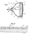
- FIG. 1 is a plan view, partially in axial section, of a color cathode-ray tube made according to the present invention.
- FIG. 2 is a section of a screen assembly of the tube shown in FIG. 1.
- FIGS. 3a-3f show selected steps in the manufacturing of the tube shown in FIG. 1.
- FIG. 1 herein shows a color CRT 10 having a glass envelope 11 comprising a rectangular faceplate panel 12 and a tubular neck 14 connected by a rectangular funnel 15.
- the funnel 15 has an internal conductive coating (not shown) that contacts an anode button 16 and extends into the neck 14.
- the panel 12 comprises a viewing faceplate or substrate 18 and a peripheral flange or sidewall 20, which is sealed to the funnel 15 by a glass frit 21.
- a three color phosphor screen 22 is carried on the inner surface of the faceplate 18. The screen 22, shown in FIG.
- a line screen which includes a multiplicity of screen elements comprised of red-emitting, green-emitting and blue-emitting phosphor stripes R, G and B, respectively, arranged in color groups or picture elements of three stripes or triads in a cyclic order and extending in a direction which is generally normal to the plane in which the electron beams are generated.
- the phosphor stripes extend in the vertical direction.
- the phosphor stripes are separated from each other by a light-absorptive matrix material 23, as is known in the art.
- the screen can be a dot screen.
- a thin conductive layer 24, preferably of aluminum, overlies the screen 22 and provides a means for applying a uniform potential to the screen as well as for reflecting light, emitted from the phosphor elements, through the faceplate 18.
- the screen 22 and the overlying aluminum layer 24 comprise a screen assembly.
- a multi-apertured color selection electrode or shadow mask 25 is removably mounted, by conventional means, in predetermined spaced relation to the screen assembly.
- An electron gun 26, shown schematically by the dashed lines in FIG. 1, is centrally mounted within the neck 14, to generate and direct three electron beams 28 along convergent paths, through the apertures in the mask 25, to the screen 22.
- the gun 26 may be, for example, a bi-potential electron gun of the type described in U.S. Pat. No. 4,620,133, issued to Morrell et al. on October 28, 1986, or any other suitable gun.
- the tube 10 is designed to be used with an external magnetic deflection yoke, such as yoke 30, located in the region of the funnel-to-neck junction.
- an external magnetic deflection yoke such as yoke 30, located in the region of the funnel-to-neck junction.
- the yoke 30 subjects the three beams 28 to magnetic fields which cause the beams to scan horizontally and vertically in a rectangular raster over the screen 22.
- the initial plane of deflection (at zero deflection) is shown by the line P-P in FIG. 1, at about the middle of the yoke 30. For simplicity, the actual curvatures of the deflection beam paths in the deflection zone are not shown.
- the screen 22 is manufactured by a novel electrophotographic process that is schematically represented In FIGS. 3a through 3f.
- the panel 12 is washed with a caustic solution, rinsed with water, etched with buffered hydrofluoric acid and rinsed once again with water, as is known in the art.
- the inner surface of the viewing faceplate 18 is then coated with a layer 32 of a suitable electrically conductive material which provides an electrode for an overlying photoconductive layer 34.
- the resultant structure is shown in FIG. 3a.
- the photoconductive layer 34 comprises a solution of a volatilizable organic polymeric material, a suitable photoconductive dye sensitive to visible light, a novel plasticizer, for a purpose to be described hereinafter, and a solvent.
- the composition and method of forming one formulation of the conductive layer 32 is described in U.S Patent No. 4,921,767.
- the photoconductive layer 34 overlying the conductive layer 32, is charged in a dark environment by a conventional positive corona discharge apparatus 36, schematically shown in FIG. 3b, which moves across the layer 34 and charges it within the range of +200 to +700 volts, +300 to +600 volts being preferred.
- the shadow mask 25 is inserted into the panel 12, and the positively-charged photoconductor is exposed, through the shadow mask, to the light from a xenon flash lamp 38 disposed within a conventional lighthouse (represented by lens 40 of FIG. 3c). After each exposure, the lamp is moved to a different position, to duplicate the incident angle of the electron beams from the electron gun.
- the first developer contains suitably prepared dry-powdered particles of a light-absorptive black matrix screen structure material.
- the black matrix material is triboelectrically charged, e.g., negatively, and expelled from the developer 42 and attracted to the positively-charged, unexposed area of the photoconductive layer 34 to directly develop that area.
- the photoconductive layer 34 containing the matrix 23, is uniformly recharged to a positive potential of about 200 to 400 volts, for the application of the first of three triboelectrically charged, dry-powdered, surface treated, color-emitting phosphor screen structure materials, which are manufactured by the processes described in U.S. Patent No 4,921,767, each of which relates to the surface treatment of phosphor particles.
- the phosphor particles are positively-charged.
- the shadow mask 25 is reinserted into the panel 12, and selected areas of the photoconductive layer 34, corresponding to the locations where green-emitting phosphor material will be deposited, are exposed to visible light from a first location within the lighthouse to selectively discharge the exposed area.
- the first light location approximates the convergence angle of the green phosphor-impinging electron beam.
- the shadow mask 25 is removed from the panel 12, and the panel is moved to a second developer 42.
- the positively-charged green-emitting phosphor particles are expelled from the developer, repelled by the positively-charged areas of the photoconductive layer 34 and matrix 23, and deposited onto the discharged, light exposed areas of the photoconductive layer, in a process known as reversal developing.
- the process of charging, exposing and developing is repeated for the dry-powdered, blue- and red-emitting, surface-treated phosphor particles of screen structure material.
- the exposure to visible light, to selectively discharge the positively-charged areas of the photoconductive layer 34, is made from a second and then from a third position within the lighthouse to approximate the convergence angles of the blue phosphor- and red phosphor-impinging electron beams, respectively.
- the matrix material and phosphors are attached to the photoconductive layer 34 by thermal or vapor bonding.
- the vapor bonding step is graphically represented in FIG. 3e, and is described in U.S. Patent No. 4,917,978, issued to Ritt et al. on April 17, 1990 and corresponding to EP-A-0 380 279 published on 01.08.90.
- the resultant structure is fixed, to further minimize displacement of the screen structure materials, as shown in FIG. 3f and as described in the last-referenced U.S. patent.
- the structure is then filmed and aluminized,as is known in the art.
- the faceplate panel 12 is baked in air at a temperature of 425°C for about 30-60 minutes to drive off the volatilizable constituents of the screen, including the conductive layer 32, the photoconductive layer 34, and the solvents present in both the screen structure and filming materials.
- the novel photoconductive layer 34 is prepared by forming a photoconductive control solution comprised of about 3.0 to 7.0,but preferably about 5.0,weight percent of a volatilizable polymeric material, such as polyvinyl carbazole (PVK); about 0.1 to 0.4, but preferably about 0.2,weight percent, relative to the PVK, of a dye sensitive to visible light, such as ethylene violet; about 0.001 weight percent, relative to the PVK, of a suitable leveling agent such as Silar-100, marketed by Silar Laboratories, Ontario, New York; and the balance, about 95 weight percent, of a solvent such as chlorobenzene.
- a photoconductive control solution comprised of about 3.0 to 7.0,but preferably about 5.0,weight percent of a volatilizable polymeric material, such as polyvinyl carbazole (PVK); about 0.1 to 0.4, but preferably about 0.2,weight percent, relative to the PVK, of a dye sensitive to visible light, such as ethylene violet; about
- the viscosity of the control solution is 65 cps.
- a suitable quantity of a plasticizer so that the concentration of the plasticizer ranges from 5 to 30 weight percent of the PVK.
- the viscosity of the plasticized control solution is adjusted to a viscosity of 45 cps by the addition of an additional quantity of the solvent.
- the preferred plasticizer is a dialkyl phthalate such as dibutylphthalate (DBP), dioctylphthalate (DOP), or diundecylphthalate (DUP).
- a control solution useful in determining the electrostatic properties of photoconductive layers having different concentrations of plasticizers has the following formulation:
- the electrostatic properties of different photoconductive layers, with and without plasticizers, were determined by applying a photoconductive solution to 48cm (19in) faceplate panels that previously had been coated with a suitable organic conductor having a thickness of about 1 micron to form the layer 32. Fourteen samples were evaluated; one sample contained a photoconductive layer 34 without a plasticizer, and the other thirteen samples comprised four classes of plasticizers having plasticizer concentrations ranging from 5 to 30 weight percent of the PVK used in the control solution.
- the plasticized photoconductive solutions were made as follows: to 200 grams of the photoconductive control solution was added a known weight percent of a plasticizer. The viscosity of the plasticized photoconductive solution was adjusted to 45 cps and coated on a 48cm faceplate panel to form a 3 to 4 micron thick layer 34 overlying the layer 32.
- the tests were conducted by charging each panel with the charging apparatus 36, which was operated at a positive voltage of 9.5kV and a current of 74 microamperes (»A). Each panel was charged for 30 seconds in an ambient atmosphere of 21°C and 68% RH. The initial voltage, Vi, was measured and the panel was held in the dark for 90 seconds, at the end of which the voltage, Vr, was read.
- the charged panel was then exposed to the light from a xenon flash lamp operated at 570 volts, 430 microfarads, and a pulse width of 1 millisecond.
- the voltage on the panel was remeasured after the initial lamp flash, and the number of flashes required to reduce the panel voltage to 10% of the voltage remaining after the 90 second dark hold, Vr, also was recorded.
- the panel was then held for 48 hours, at room temperature and at 75% RH, and visually evaluated for cracks in the photoconductive layer.
- Several of the panels that exhibited no cracks in the photoreceptor i.e., conductive layer 32 and photoconductive layer 34
- dialkyl phthalates more specifically, dibutylphthalate (DBP), dioctylphthalate (DOP), and diundecylphthalate (DUP);
- dialkyl adipates i.e., di-2-ethyl hexyl adipate (marketed as Plastolein-9066, from Quantum Chemical Corp., Cincinnati, OH);
- di-2-ethyl hexyl azelate marketed as Plastolein-9058, also from Quantum Chemical Corp.
- terpene resins marketed as Cumar-21, from Neville Chemical Co., Pittsburgh, PA.
- the materials of classes 2 and 4 correspond to materials known in the prior art, and the material of class 3 is related to class 2. None of the materials in classes 2 through 4 is included within the group of diesters of phthalatic acids recited in class 1.
- samples 3 through 9 representing plasticizer concentrations of 10 to 30 wt %, showed no cracking of the photoreceptor layer (i.e., layer 34) when held at 75% RH for 48 hours.
- samples 4, 5 (both DOP) and 7 (DUP) were filmed because it was believed that the higher concentrations of plasticizers, i.e., from 20 to 30 wt % of the PVK, would provide the necessary flexibility to the photoreceptor layer.
Description
- The present invention relates to a method of electrophotographically manufacturing a luminescent screen assembly and, more particularly, to a method in which an improved plasticizer is utilized with a photoconductive layer to minimize the cracking of the layer.
- U.S. Patent No. 3,475,169, issued to Lange on October 28, 1969, discloses a process of electrophotographically screening color cathode-ray tubes by applying, over the image area, a conductive layer and a superimposed photoconductive layer preferably formed of a resin. A latent charge image is established on the photoconductive layer,and then a developer is applied over the image area. The developer includes phosphor particles as well as a binder in a carrier liquid. Preferably, the binder is formed of the same resin as that included in the photoconductive layer and the resin encapsulates the phosphor particles. The application of the developer selectively deposits phosphor particles to develop the latent image, and thereafter the excess developer is removed and the image is dried. For a color screen, this same general process is carried out three times, once for each of the three color-emitting phosphors. The photoconductive layer tends to be hard and brittle so it is known to add a plasticizer, such as Piccolastic A-75 (a polymerized styrene homologue) or Piccoumaron 410-L (a terpene compound), each of which is a product of Pennsylvania Industrial Chemical Corp., to prevent cracking of the photoconductive layer and subsequent misregister of the phosphors. Alternatively, Plastolein 9066 LT (di-2-ethyl hexyl adipate), a product of Emery Industries, Inc., may be used. Using either of the two former-named materials, the ratio of plasticizer to resin (PVK, i.e., polyvinyl carbazole) is 1:1; whereas, for the latter-named material, the plasticizer comprises about 13.3 weight percent of the resin. Plastolein 9066 LT is disclosed in U.S. Patent No. 3,489,556,issued to Drozd on January 13, 1970, and in U.S. Patent No. 3,489,557, issued to Lange et al. on January 13, 1970.
- U.S. Patent No. 4,921,767, issued to Datta et al. on May 1, 1990, and corresponding to EP-A-0 378 911 published on 25.07.90 discloses a "dry" process for forming a CRT screen assembly. The "dry" process utilizes triboelectrically charged dry phosphor particles rather than phosphor particles suspended in a carrier liquid. The "dry" triboelectrically-charged phosphor develops the latent charge image formed on the photoconductive layer. The "dry" process requires fewer processing steps and is, therefore, more efficient than the process of U.S. Patent No. 3,475,169. The initial steps in the "dry" process are similar to those described in the earlier patent, in that a conductive layer and an overlying photoconductive layer are formed in the image area of the screen and a latent charge image is formed on the photoconductive layer. In the process disclosed in U.S. Patent No. 4,921,767, the photoconductive layer does not contain a plasticizer because the aforementioned plasticizers (or their equivalents) are not capable of providing the critical electrical parameters of charge acceptance, light and dark decay rates, and light sensitivity without degradation, in the concentration of plasticizer necessary to prevent cracking of the PVK-based photoconductive layer.
- In accordance with the present invention, a method of electrophotographically manufacturing a luminescent screen assembly on a substrate for use within a CRT includes the steps of forming a conductive layer on the substrate, overcoating the conductive layer with a photoconductive layer, establishing an electrostatic charge on the photoconductive layer and exposing selected areas of the photoconductive layer to visible light to affect the charge thereon. Then, the photoconductive layer is developed with charged screen structure material. The improved process improves the integrity of the photoconductive layer by adding a dialkyl phthalate plasticizer selected from the group consisting of dibutylphthalate (DBP), dioctylphthalate (DOP), and diundecylphthalate (DUP).
- In the drawings:
- FIG. 1 is a plan view, partially in axial section, of a color cathode-ray tube made according to the present invention.
- FIG. 2 is a section of a screen assembly of the tube shown in FIG. 1.
- FIGS. 3a-3f show selected steps in the manufacturing of the tube shown in FIG. 1.
- Generally, the details of the inventive method are similar to those of the method described in the previously cited U.S. Patent No. 4,921,767,
except for the composition of the photoconductive layer. - Briefly, FIG. 1 herein shows a
color CRT 10 having a glass envelope 11 comprising arectangular faceplate panel 12 and atubular neck 14 connected by arectangular funnel 15. Thefunnel 15 has an internal conductive coating (not shown) that contacts ananode button 16 and extends into theneck 14. Thepanel 12 comprises a viewing faceplate orsubstrate 18 and a peripheral flange orsidewall 20, which is sealed to thefunnel 15 by a glass frit 21. A threecolor phosphor screen 22 is carried on the inner surface of thefaceplate 18. Thescreen 22, shown in FIG. 2, preferably is a line screen which includes a multiplicity of screen elements comprised of red-emitting, green-emitting and blue-emitting phosphor stripes R, G and B, respectively, arranged in color groups or picture elements of three stripes or triads in a cyclic order and extending in a direction which is generally normal to the plane in which the electron beams are generated. In the normal viewing position for this embodiment, the phosphor stripes extend in the vertical direction. Preferably, the phosphor stripes are separated from each other by a light-absorptive matrix material 23, as is known in the art. Alternatively, the screen can be a dot screen. A thinconductive layer 24, preferably of aluminum, overlies thescreen 22 and provides a means for applying a uniform potential to the screen as well as for reflecting light, emitted from the phosphor elements, through thefaceplate 18. Thescreen 22 and theoverlying aluminum layer 24 comprise a screen assembly. - With respect again to FIG. 1, a multi-apertured color selection electrode or
shadow mask 25 is removably mounted, by conventional means, in predetermined spaced relation to the screen assembly. Anelectron gun 26, shown schematically by the dashed lines in FIG. 1, is centrally mounted within theneck 14, to generate and direct threeelectron beams 28 along convergent paths, through the apertures in themask 25, to thescreen 22. Thegun 26 may be, for example, a bi-potential electron gun of the type described in U.S. Pat. No. 4,620,133, issued to Morrell et al. on October 28, 1986, or any other suitable gun. - The
tube 10 is designed to be used with an external magnetic deflection yoke, such asyoke 30, located in the region of the funnel-to-neck junction. When activated, theyoke 30 subjects the threebeams 28 to magnetic fields which cause the beams to scan horizontally and vertically in a rectangular raster over thescreen 22. The initial plane of deflection (at zero deflection) is shown by the line P-P in FIG. 1, at about the middle of theyoke 30. For simplicity, the actual curvatures of the deflection beam paths in the deflection zone are not shown. - The
screen 22 is manufactured by a novel electrophotographic process that is schematically represented In FIGS. 3a through 3f. Initially, thepanel 12 is washed with a caustic solution, rinsed with water, etched with buffered hydrofluoric acid and rinsed once again with water, as is known in the art. The inner surface of theviewing faceplate 18 is then coated with alayer 32 of a suitable electrically conductive material which provides an electrode for an overlyingphotoconductive layer 34. The resultant structure is shown in FIG. 3a. Thephotoconductive layer 34 comprises a solution of a volatilizable organic polymeric material, a suitable photoconductive dye sensitive to visible light, a novel plasticizer, for a purpose to be described hereinafter, and a solvent. The composition and method of forming one formulation of theconductive layer 32 is described in U.S Patent No. 4,921,767. - The
photoconductive layer 34, overlying theconductive layer 32, is charged in a dark environment by a conventional positivecorona discharge apparatus 36, schematically shown in FIG. 3b, which moves across thelayer 34 and charges it within the range of +200 to +700 volts, +300 to +600 volts being preferred. Theshadow mask 25 is inserted into thepanel 12, and the positively-charged photoconductor is exposed, through the shadow mask, to the light from axenon flash lamp 38 disposed within a conventional lighthouse (represented by lens 40 of FIG. 3c). After each exposure, the lamp is moved to a different position, to duplicate the incident angle of the electron beams from the electron gun. Three exposures are required, from three different lamp positions, to discharge the areas of the photoconductor where the light-emitting phosphors subsequently will be deposited to form the screen. After the exposure step, theshadow mask 25 is removed from thepanel 12, and the panel is moved to a first developer 42 (FIG. 3d). The first developer contains suitably prepared dry-powdered particles of a light-absorptive black matrix screen structure material. The black matrix material is triboelectrically charged, e.g., negatively, and expelled from thedeveloper 42 and attracted to the positively-charged, unexposed area of thephotoconductive layer 34 to directly develop that area. - The
photoconductive layer 34, containing thematrix 23, is uniformly recharged to a positive potential of about 200 to 400 volts, for the application of the first of three triboelectrically charged, dry-powdered, surface treated, color-emitting phosphor screen structure materials, which are manufactured by the processes described in U.S. Patent No 4,921,767, each of which relates to the surface treatment of phosphor particles. Preferably, the phosphor particles are positively-charged. Theshadow mask 25 is reinserted into thepanel 12, and selected areas of thephotoconductive layer 34, corresponding to the locations where green-emitting phosphor material will be deposited, are exposed to visible light from a first location within the lighthouse to selectively discharge the exposed area. The first light location approximates the convergence angle of the green phosphor-impinging electron beam. Theshadow mask 25 is removed from thepanel 12, and the panel is moved to asecond developer 42. The positively-charged green-emitting phosphor particles are expelled from the developer, repelled by the positively-charged areas of thephotoconductive layer 34 andmatrix 23, and deposited onto the discharged, light exposed areas of the photoconductive layer, in a process known as reversal developing. - The process of charging, exposing and developing is repeated for the dry-powdered, blue- and red-emitting, surface-treated phosphor particles of screen structure material. The exposure to visible light, to selectively discharge the positively-charged areas of the
photoconductive layer 34, is made from a second and then from a third position within the lighthouse to approximate the convergence angles of the blue phosphor- and red phosphor-impinging electron beams, respectively. - The matrix material and phosphors are attached to the
photoconductive layer 34 by thermal or vapor bonding. The vapor bonding step is graphically represented in FIG. 3e, and is described in U.S. Patent No. 4,917,978, issued to Ritt et al. on April 17, 1990 and corresponding to EP-A-0 380 279 published on 01.08.90. Subsequently, the resultant structure is fixed, to further minimize displacement of the screen structure materials, as shown in FIG. 3f and as described in the last-referenced U.S. patent. - The structure is then filmed and aluminized,as is known in the art. The
faceplate panel 12 is baked in air at a temperature of 425°C for about 30-60 minutes to drive off the volatilizable constituents of the screen, including theconductive layer 32, thephotoconductive layer 34, and the solvents present in both the screen structure and filming materials. - The novel
photoconductive layer 34 is prepared by forming a photoconductive control solution comprised of about 3.0 to 7.0,but preferably about 5.0,weight percent of a volatilizable polymeric material, such as polyvinyl carbazole (PVK); about 0.1 to 0.4, but preferably about 0.2,weight percent, relative to the PVK, of a dye sensitive to visible light, such as ethylene violet; about 0.001 weight percent, relative to the PVK, of a suitable leveling agent such as Silar-100, marketed by Silar Laboratories, Scotia, New York; and the balance, about 95 weight percent, of a solvent such as chlorobenzene. The solution is mixed thoroughly and filtered through a 1 micron filter. The viscosity of the control solution is 65 cps. To this control solution is added a suitable quantity of a plasticizer so that the concentration of the plasticizer ranges from 5 to 30 weight percent of the PVK. The viscosity of the plasticized control solution is adjusted to a viscosity of 45 cps by the addition of an additional quantity of the solvent. The preferred plasticizer is a dialkyl phthalate such as dibutylphthalate (DBP), dioctylphthalate (DOP), or diundecylphthalate (DUP). - By way of example, a control solution useful in determining the electrostatic properties of photoconductive layers having different concentrations of plasticizers has the following formulation:

- The electrostatic properties of different photoconductive layers, with and without plasticizers, were determined by applying a photoconductive solution to 48cm (19in) faceplate panels that previously had been coated with a suitable organic conductor having a thickness of about 1 micron to form the
layer 32. Fourteen samples were evaluated; one sample contained aphotoconductive layer 34 without a plasticizer, and the other thirteen samples comprised four classes of plasticizers having plasticizer concentrations ranging from 5 to 30 weight percent of the PVK used in the control solution. - The plasticized photoconductive solutions were made as follows: to 200 grams of the photoconductive control solution was added a known weight percent of a plasticizer. The viscosity of the plasticized photoconductive solution was adjusted to 45 cps and coated on a 48cm faceplate panel to form a 3 to 4 micron
thick layer 34 overlying thelayer 32. - The electrostatic properties of the photoconductive layer that are of interest include the initial electrostatic surface voltage acceptance, (Vi), of the coated panel, the voltage remaining, (Vr), after the panel is held in the dark for a given period of time,s, and the rate of dark decay (V/s where V = Vi-Vr). The tests were conducted by charging each panel with the charging
apparatus 36, which was operated at a positive voltage of 9.5kV and a current of 74 microamperes (»A). Each panel was charged for 30 seconds in an ambient atmosphere of 21°C and 68% RH. The initial voltage, Vi, was measured and the panel was held in the dark for 90 seconds, at the end of which the voltage, Vr, was read. - The charged panel was then exposed to the light from a xenon flash lamp operated at 570 volts, 430 microfarads, and a pulse width of 1 millisecond. The voltage on the panel was remeasured after the initial lamp flash, and the number of flashes required to reduce the panel voltage to 10% of the voltage remaining after the 90 second dark hold, Vr, also was recorded. The panel was then held for 48 hours, at room temperature and at 75% RH, and visually evaluated for cracks in the photoconductive layer. Several of the panels that exhibited no cracks in the photoreceptor (i.e.,
conductive layer 32 and photoconductive layer 34) were then screened, filmed and reexamined. The results are summarized in the TABLE.
- Sample 1 was a control sample in which no plasticizer was added to the control solution. While the initial charge acceptance of the
photoconductive layer 34 to the charge provided by theapparatus 36 was good (Vi = 590 volts), the charge remaining on the photoconductive layer after being held in the dark for 90 seconds also was good (470 volts), and the dark decay of the voltage (Vi-Vr/s =
- The plasticizers selected for evaluation fell into four general classes: (1) dialkyl phthalates, more specifically, dibutylphthalate (DBP), dioctylphthalate (DOP), and diundecylphthalate (DUP); (2) dialkyl adipates, i.e., di-2-ethyl hexyl adipate (marketed as Plastolein-9066, from Quantum Chemical Corp., Cincinnati, OH); (3) di-2-ethyl hexyl azelate (marketed as Plastolein-9058, also from Quantum Chemical Corp.); and (4) terpene resins (marketed as Cumar-21, from Neville Chemical Co., Pittsburgh, PA). The materials of classes 2 and 4 correspond to materials known in the prior art, and the material of class 3 is related to class 2. None of the materials in classes 2 through 4 is included within the group of diesters of phthalatic acids recited in class 1.
- Again with reference to the TABLE, with the exception of the sample 2 (5 wt % DOP), samples 3 through 9, representing plasticizer concentrations of 10 to 30 wt %, showed no cracking of the photoreceptor layer (i.e., layer 34) when held at 75% RH for 48 hours. The charge acceptance, i.e., the initial voltage, Vi, on samples 3 through 9, as well as the voltage remaining after a 90 second dark hold, Vr, decreased with increasing concentrations of plasticizer. Only samples 4, 5 (both DOP) and 7 (DUP) were filmed because it was believed that the higher concentrations of plasticizers, i.e., from 20 to 30 wt % of the PVK, would provide the necessary flexibility to the photoreceptor layer. The charge acceptance and retention of the DOP and DUP samples exceeded that of the DBP samples so that the two former materials in concentrations of 10 to 30 wt % and 10 to 20 wt % were preferred over the two DBP samples (8 and 9); although, DBP was an acceptable material.
Samples 10 and 11 (Plastolein-9066) were unacceptable for use in the "dry" process described herein because of cracking (sample 10) of the photoreceptor layer, or no light sensitivity of the layer, at a plasticizer concentration of 20 wt % (sample 11).Sample 12 also was unacceptable since a 10 wt % concentration of Plastolein-9058 exhibited no light sensitivity. Whilesamples 13 and 14 exhibited outstanding charge acceptance (Vi) and charge retention (Vr) ability, both samples, utilizing 10 and 20 wt % concentration of Cumar-21, exhibited cracks in the photoreceptor layer after the 48 hour hold at 75% RH.
Claims (3)
- A method of electrophotographically manufacturing a luminescent screen assembly (22,24) on a substrate (18) for use within a CRT (10), including the steps of:a) forming a conductive layer (32) on said substrate;b) overcoating said conductive layer with a photoconductive solution, said solution comprising an organic polymeric material, a suitable photoconductive dye, a plasticizer, and a solvent, to form a photoconductive layer (34);c) establishing an electrostatic charge on said photoconductive layer;d) exposing selected areas of said photoconductive layer to visible light to affect the charge thereon; ande) developing said photoconductive layer with charged screen structure material, wherein said plasticizer is a dialkyl phthalate selected from the group consisting of dibutylphthalate (DBP), dioctylphthalate (DOP), and diundecylphthalate (DUP).
- The method of claim 1, characterized in that the concentration of said plasticizer ranges from about 10 to 30 weight percent of said organic polymeric material.
- The method of claim 2, characterized in that the concentration of said plasticizer ranges from about 20 to 30 percent of said organic polymeric material.
Applications Claiming Priority (2)
| Application Number | Priority Date | Filing Date | Title |
|---|---|---|---|
| US49500290A | 1990-03-12 | 1990-03-12 | |
| US495002 | 1990-03-12 |
Publications (3)
| Publication Number | Publication Date |
|---|---|
| EP0447078A2 EP0447078A2 (en) | 1991-09-18 |
| EP0447078A3 EP0447078A3 (en) | 1991-11-13 |
| EP0447078B1 true EP0447078B1 (en) | 1994-09-28 |
Family
ID=23966834
Family Applications (1)
| Application Number | Title | Priority Date | Filing Date |
|---|---|---|---|
| EP91301706A Expired - Lifetime EP0447078B1 (en) | 1990-03-12 | 1991-03-01 | Method of electrophotographically manufacturing a luminescent screen assembly for a CRT |
Country Status (5)
| Country | Link |
|---|---|
| US (1) | US5135826A (en) |
| EP (1) | EP0447078B1 (en) |
| JP (1) | JPH088065B2 (en) |
| KR (1) | KR940000446B1 (en) |
| DE (1) | DE69104245T2 (en) |
Families Citing this family (11)
| Publication number | Priority date | Publication date | Assignee | Title |
|---|---|---|---|---|
| DE69218288T2 (en) * | 1991-05-23 | 1997-06-26 | Matsushita Electric Ind Co Ltd | Holographic recording material, device for recording a hologram, method for its production and recording method |
| US5413885A (en) * | 1993-12-22 | 1995-05-09 | Rca Thompson Licensing Corp. | Organic photoconductor for an electrophotographic screening process for a CRT |
| US5370952A (en) * | 1993-12-22 | 1994-12-06 | Rca Thomson Licensing Corp. | Organic conductor for an electrophotographic screening process for a CRT |
| US5405722A (en) * | 1993-12-22 | 1995-04-11 | Rca Thomson Licensing Corp. | Method for combined baking-out and sealing of an electrophotographically processed screen assembly for a cathode-ray tube |
| US5474867A (en) * | 1994-09-16 | 1995-12-12 | Thomson Consumer Electronics, Inc. | Method of manufacturing a luminescent screen for a CRT under ambient controls |
| US5554468A (en) * | 1995-04-27 | 1996-09-10 | Thomson Consumer Electronics, Inc. | CRT electrophotographic screening method using an organic photoconductive layer |
| DE19630016C2 (en) * | 1996-07-25 | 2000-10-12 | Daimler Chrysler Ag | Method for producing a phosphor layer of a cathode ray tube |
| US6037086A (en) * | 1998-06-16 | 2000-03-14 | Thomson Consumer Electronics, Inc., | Method of manufacturing a matrix for a cathode-ray tube |
| US6218408B1 (en) | 1999-06-30 | 2001-04-17 | Synaptic Pharmaceutical Corporation | Selective NPY (Y5) antagonists (bicyclics) |
| JP2005062307A (en) * | 2003-08-08 | 2005-03-10 | Fujitsu Hitachi Plasma Display Ltd | Method for manufacturing flat-panel display |
| US7358015B2 (en) | 2005-06-03 | 2008-04-15 | Lexmark International, Inc. | Plasticized photoconductor |
Family Cites Families (12)
| Publication number | Priority date | Publication date | Assignee | Title |
|---|---|---|---|---|
| US3067055A (en) * | 1959-08-05 | 1962-12-04 | Rca Corp | Metallized phosphor screens and method of making same |
| US3475169A (en) * | 1965-08-20 | 1969-10-28 | Zenith Radio Corp | Process of electrostatically screening color cathode-ray tubes |
| US3489556A (en) * | 1966-03-16 | 1970-01-13 | Zenith Radio Corp | Process fo electrostatically screening color cathode-ray tubes |
| US3489557A (en) * | 1966-03-16 | 1970-01-13 | Zenith Radio Corp | Process of electrostatically screening a color cathode-ray tube |
| JPS4938315A (en) * | 1972-08-25 | 1974-04-10 | ||
| JPS54130936A (en) * | 1978-03-31 | 1979-10-11 | Canon Inc | Zerographic photosensitive element |
| JPS5694360A (en) * | 1979-12-28 | 1981-07-30 | Ricoh Co Ltd | Electrophotographic receptor |
| JPS5814444A (en) * | 1981-07-20 | 1983-01-27 | Hitachi Ltd | Formation of fluorescent screen for cathode-ray tube |
| JPS5931964A (en) * | 1982-08-16 | 1984-02-21 | Fuji Photo Film Co Ltd | Disazo compound, photoconductive composition containing it and electrophotographic receptor |
| US4921767A (en) * | 1988-12-21 | 1990-05-01 | Rca Licensing Corp. | Method of electrophotographically manufacturing a luminescent screen assembly for a cathode-ray-tube |
| US4917978A (en) * | 1989-01-23 | 1990-04-17 | Thomson Consumer Electronics, Inc. | Method of electrophotographically manufacturing a luminescent screen assembly having increased adherence for a CRT |
| US5028501A (en) * | 1989-06-14 | 1991-07-02 | Rca Licensing Corp. | Method of manufacturing a luminescent screen assembly using a dry-powdered filming material |
-
1991
- 1991-03-01 DE DE69104245T patent/DE69104245T2/en not_active Expired - Fee Related
- 1991-03-01 EP EP91301706A patent/EP0447078B1/en not_active Expired - Lifetime
- 1991-03-11 KR KR1019910003853A patent/KR940000446B1/en not_active IP Right Cessation
- 1991-03-12 JP JP3073901A patent/JPH088065B2/en not_active Expired - Fee Related
- 1991-04-29 US US07/692,967 patent/US5135826A/en not_active Expired - Lifetime
Also Published As
| Publication number | Publication date |
|---|---|
| US5135826A (en) | 1992-08-04 |
| DE69104245T2 (en) | 1995-04-06 |
| JPH04220930A (en) | 1992-08-11 |
| EP0447078A3 (en) | 1991-11-13 |
| KR940000446B1 (en) | 1994-01-21 |
| JPH088065B2 (en) | 1996-01-29 |
| DE69104245D1 (en) | 1994-11-03 |
| EP0447078A2 (en) | 1991-09-18 |
Similar Documents
| Publication | Publication Date | Title |
|---|---|---|
| EP0378911B1 (en) | Method of electrophotographically manufacturing a luminescent screen assembly for a cathode-ray tube | |
| CA2008073C (en) | Method of electrophotographically manufacturing a luminescent screen assembly for a crt | |
| JPH0853667A (en) | Cathode-ray tube | |
| EP0447078B1 (en) | Method of electrophotographically manufacturing a luminescent screen assembly for a CRT | |
| KR0141521B1 (en) | Method for combined baking out and sealing of an electrophotographically processed screen assembly for a cathode ray tube | |
| US5012155A (en) | Surface treatment of phosphor particles and method for a CRT screen | |
| CA2138188C (en) | Crt electrophotographic screening method using an organic photoconductor | |
| US5156770A (en) | Conductive contact patch for a CRT faceplate panel | |
| KR0158023B1 (en) | Organic conductor for an electrophotographic screening process for crt | |
| US5151337A (en) | Method of electrophotographically manufacturing a luminescent screen for a color CRT having a conductive contact patch | |
| EP0740325B1 (en) | CRT Electrophotographic screening method using an organic photoconductive layer | |
| EP0375229B1 (en) | Surface treatment of phosphor particles and method for a crt screen | |
| EP1079411B1 (en) | Electrophotographic screening method with humidity and temperature insensitive organic conductor | |
| US5407765A (en) | Method of spray-depositing an organic conductor to make a screen assembly for a CRT | |
| EP1103061B1 (en) | Method of manufacturing a phosphor screen for a crt | |
| US6165657A (en) | Method of electrophotographically manufacturing a luminescent screen assembly for a CRT and a CRT comprising a luminescent screen assembly manufactured by the method |
Legal Events
| Date | Code | Title | Description |
|---|---|---|---|
| PUAI | Public reference made under article 153(3) epc to a published international application that has entered the european phase |
Free format text: ORIGINAL CODE: 0009012 |
|
| AK | Designated contracting states |
Kind code of ref document: A2 Designated state(s): DE FR GB IT |
|
| PUAL | Search report despatched |
Free format text: ORIGINAL CODE: 0009013 |
|
| AK | Designated contracting states |
Kind code of ref document: A3 Designated state(s): DE FR GB IT |
|
| 17P | Request for examination filed |
Effective date: 19920511 |
|
| RAP1 | Party data changed (applicant data changed or rights of an application transferred) |
Owner name: RCA THOMSON LICENSING CORPORATION Owner name: THOMSON CONSUMER ELECTRONICS, INC. |
|
| 17Q | First examination report despatched |
Effective date: 19940126 |
|
| GRAA | (expected) grant |
Free format text: ORIGINAL CODE: 0009210 |
|
| AK | Designated contracting states |
Kind code of ref document: B1 Designated state(s): DE FR GB IT |
|
| REF | Corresponds to: |
Ref document number: 69104245 Country of ref document: DE Date of ref document: 19941103 |
|
| ET | Fr: translation filed | ||
| ITF | It: translation for a ep patent filed |
Owner name: ING. C. GREGORJ S.P.A. |
|
| PLBE | No opposition filed within time limit |
Free format text: ORIGINAL CODE: 0009261 |
|
| STAA | Information on the status of an ep patent application or granted ep patent |
Free format text: STATUS: NO OPPOSITION FILED WITHIN TIME LIMIT |
|
| 26N | No opposition filed | ||
| REG | Reference to a national code |
Ref country code: GB Ref legal event code: IF02 |
|
| REG | Reference to a national code |
Ref country code: FR Ref legal event code: D6 |
|
| REG | Reference to a national code |
Ref country code: GB Ref legal event code: 746 Effective date: 20030103 |
|
| PGFP | Annual fee paid to national office [announced via postgrant information from national office to epo] |
Ref country code: GB Payment date: 20030207 Year of fee payment: 13 |
|
| PGFP | Annual fee paid to national office [announced via postgrant information from national office to epo] |
Ref country code: FR Payment date: 20030318 Year of fee payment: 13 |
|
| PGFP | Annual fee paid to national office [announced via postgrant information from national office to epo] |
Ref country code: DE Payment date: 20030422 Year of fee payment: 13 |
|
| PG25 | Lapsed in a contracting state [announced via postgrant information from national office to epo] |
Ref country code: GB Free format text: LAPSE BECAUSE OF NON-PAYMENT OF DUE FEES Effective date: 20040301 |
|
| PG25 | Lapsed in a contracting state [announced via postgrant information from national office to epo] |
Ref country code: DE Free format text: LAPSE BECAUSE OF NON-PAYMENT OF DUE FEES Effective date: 20041001 |
|
| GBPC | Gb: european patent ceased through non-payment of renewal fee | ||
| PG25 | Lapsed in a contracting state [announced via postgrant information from national office to epo] |
Ref country code: FR Free format text: LAPSE BECAUSE OF NON-PAYMENT OF DUE FEES Effective date: 20041130 |
|
| REG | Reference to a national code |
Ref country code: FR Ref legal event code: ST |
|
| PG25 | Lapsed in a contracting state [announced via postgrant information from national office to epo] |
Ref country code: IT Free format text: LAPSE BECAUSE OF NON-PAYMENT OF DUE FEES;WARNING: LAPSES OF ITALIAN PATENTS WITH EFFECTIVE DATE BEFORE 2007 MAY HAVE OCCURRED AT ANY TIME BEFORE 2007. THE CORRECT EFFECTIVE DATE MAY BE DIFFERENT FROM THE ONE RECORDED. Effective date: 20050301 |