EP0443248A2 - Liquid crystal display device - Google Patents
Liquid crystal display device Download PDFInfo
- Publication number
- EP0443248A2 EP0443248A2 EP90313182A EP90313182A EP0443248A2 EP 0443248 A2 EP0443248 A2 EP 0443248A2 EP 90313182 A EP90313182 A EP 90313182A EP 90313182 A EP90313182 A EP 90313182A EP 0443248 A2 EP0443248 A2 EP 0443248A2
- Authority
- EP
- European Patent Office
- Prior art keywords
- liquid crystal
- display device
- crystal display
- driving
- ratio
- Prior art date
- Legal status (The legal status is an assumption and is not a legal conclusion. Google has not performed a legal analysis and makes no representation as to the accuracy of the status listed.)
- Withdrawn
Links
- 239000004973 liquid crystal related substance Substances 0.000 title claims abstract description 98
- 210000002858 crystal cell Anatomy 0.000 claims abstract description 24
- 239000000463 material Substances 0.000 claims abstract description 18
- 238000000034 method Methods 0.000 claims abstract description 14
- 239000000758 substrate Substances 0.000 claims abstract description 12
- 239000004988 Nematic liquid crystal Substances 0.000 claims abstract description 6
- 239000000203 mixture Substances 0.000 description 26
- 150000001875 compounds Chemical class 0.000 description 6
- OKTJSMMVPCPJKN-UHFFFAOYSA-N Carbon Chemical compound [C] OKTJSMMVPCPJKN-UHFFFAOYSA-N 0.000 description 4
- 125000000217 alkyl group Chemical group 0.000 description 4
- 229910052799 carbon Inorganic materials 0.000 description 4
- 125000006850 spacer group Chemical group 0.000 description 3
- 230000003068 static effect Effects 0.000 description 3
- 230000000694 effects Effects 0.000 description 2
- 210000004027 cell Anatomy 0.000 description 1
- 230000006866 deterioration Effects 0.000 description 1
- 239000000126 substance Substances 0.000 description 1
- 238000002834 transmittance Methods 0.000 description 1
Images


Classifications
-
- G—PHYSICS
- G09—EDUCATION; CRYPTOGRAPHY; DISPLAY; ADVERTISING; SEALS
- G09G—ARRANGEMENTS OR CIRCUITS FOR CONTROL OF INDICATING DEVICES USING STATIC MEANS TO PRESENT VARIABLE INFORMATION
- G09G3/00—Control arrangements or circuits, of interest only in connection with visual indicators other than cathode-ray tubes
- G09G3/20—Control arrangements or circuits, of interest only in connection with visual indicators other than cathode-ray tubes for presentation of an assembly of a number of characters, e.g. a page, by composing the assembly by combination of individual elements arranged in a matrix no fixed position being assigned to or needed to be assigned to the individual characters or partial characters
- G09G3/34—Control arrangements or circuits, of interest only in connection with visual indicators other than cathode-ray tubes for presentation of an assembly of a number of characters, e.g. a page, by composing the assembly by combination of individual elements arranged in a matrix no fixed position being assigned to or needed to be assigned to the individual characters or partial characters by control of light from an independent source
- G09G3/36—Control arrangements or circuits, of interest only in connection with visual indicators other than cathode-ray tubes for presentation of an assembly of a number of characters, e.g. a page, by composing the assembly by combination of individual elements arranged in a matrix no fixed position being assigned to or needed to be assigned to the individual characters or partial characters by control of light from an independent source using liquid crystals
- G09G3/3611—Control of matrices with row and column drivers
-
- G—PHYSICS
- G09—EDUCATION; CRYPTOGRAPHY; DISPLAY; ADVERTISING; SEALS
- G09G—ARRANGEMENTS OR CIRCUITS FOR CONTROL OF INDICATING DEVICES USING STATIC MEANS TO PRESENT VARIABLE INFORMATION
- G09G2320/00—Control of display operating conditions
- G09G2320/02—Improving the quality of display appearance
- G09G2320/0209—Crosstalk reduction, i.e. to reduce direct or indirect influences of signals directed to a certain pixel of the displayed image on other pixels of said image, inclusive of influences affecting pixels in different frames or fields or sub-images which constitute a same image, e.g. left and right images of a stereoscopic display
Definitions
- the present invention relates to a liquid crystal display device of a super twisted nematic type.
- Methods for driving a liquid crystal display device are classified into two categories, i.e. a static drive method and a multiplex drive method.
- a static drive method a signal voltage is continuously applied to the electrodes of the display device during display on a "one pixel at a time” basis.
- a multiplex drive method a signal voltage for providing a display is applied to the electrodes in a time-sharing manner on a "one line at a time” basis. The latter is widely used in display devices since the number of driving elements and lead terminals therefor is far reduced by contrast with the static drive method.
- a duty ratio for the driving is expressed in general by 1/Nx (where "Nx" is the number of scanning lines in the display).
- the applied driving signal voltage is required to be higher.
- an integrated circuit (IC) having a high withstand voltage which is used in the display device, requires a driving voltage of not more than 2 ⁇ N V. Since the withstand voltage of the IC is limited, the threshold voltage of a liquid crystal cell of the display device must be lowered in order to drive the display device using the most suitable bias ratio. A definition of the threshold voltage will be given later in this specification.
- the present invention provides a liquid crystal display device capable of obtaining a high contrast in its display and also a rapid response speed at a duty ratio of 1/N (N ⁇ 300) with a driving voltage of not more than 2 ⁇ N V.
- a liquid crystal display device comprising a liquid crystal cell including a layer of a nematic liquid crystal material interposed between a pair of electrode substrates, the nematic liquid crystal material having a twist angle in the range of 180° to 360°, a pair of polarising plates disposed on opposite sides of the liquid crystal cell, and means for driving the liquid crystal cell by a multiplex drive technique characterised in that the means for driving the liquid crystal cell are arranged to apply a driving voltage of not more than 2 ⁇ N V at a duty ratio of 1/N and a driving bias ratio in the range from 1/( ⁇ N -N/200) to 1/( ⁇ N -N/50), where N ⁇ 300.
- a liquid crystal display device is shown in Figure 1 and comprises a multiplex drive circuit 1, a liquid crystal cell 2, an upper electrode substrate 3 and a lower electrode substrate 4, respectively, a spacer 5, a liquid crystal layer 6, and an upper polarising plate 8 and a lower polarising plate 9, respectively.
- the liquid crystal cell 2 includes the upper electrode substrate 3, the liquid crystal layer 6, the spacer 5, and the lower electrode substrate 4.
- the upper electrode substrate 3 and the lower electrode substrate 4 are spaced by the spacer 5 at a predetermined distance, and the liquid crystal layer 6 is disposed between the upper electrode substrate 3 and the lower electrode substrate 4.
- the liquid crystal cell 2 is disposed between the upper polarizing plate 8 and the lower polarising plate 9. It is preferable to insert an optically anisotropic substance between the upper polarising plate 8 and the upper electrode substrate 3.
- the multiplex drive circuit 1 is connected to the liquid crystal cell 2, and generates time-sharing signals to drive the cell 2.
- FIG 2 shows a representative wave form for the driving signals applied to the liquid crystal cell 2 from the multiplex drive circuit 1 of the liquid crystal display device shown in Figure 1.
- the wave form has a duty ratio, which is 1/N, and a bias ratio, which is 1/M.
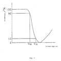
- Figure 3 shows a characteristic for the brightness, in the vertical direction, against applied voltage in a liquid crystal display device of a super twisted type as shown in Figure 1.
- the value ⁇ is more than 1.
- the multiplex drive characteristic is improved as the value ⁇ approximates 1.
- Figure 4 shows various values ⁇ against the threshold voltage Vth/V for the liquid crystal cell when a twist angle of liquid crystal material is 240°, in the embodiment shown in Figure 1.
- the threshold voltage Vth/V is lowered, the value ⁇ becomes large, and accordingly the multiplex drive characteristic is degraded.
- the threshold voltage Vth/V is further lowered less than 1.8 V, the value ⁇ steeply increases, and consequently the multiplex drive characteristic deteriorates further suddenly.
- R1 to R8 represent chain alkyl groups having carbon values of 1 to 9.
- the driving voltage is 25 V ( ⁇ 2 x ⁇ 400 V)
- the bias ratio is varied
- the most suitable liquid crystal material has been selected from the liquid crystal compositions "A" to "E” in Table 1.
- Table 2 shows such display characteristics of the liquid crystal display device.
- This fact shows that a liquid crystal display device having improved contrast and a higher response speed is obtained using a bias ratio ranging from 1/( ⁇ N -N/200) to 1/( ⁇ N -N/50).
- a liquid crystal display device having still better display characteristics can be obtained when the bias ratio ranges from 1/( ⁇ N -N/150) to 1/( ⁇ N -N/75).
- the bias ratio is varied
- the most suitable liquid crystal material has been selected from the liquid crystal compositions "A" to "H” in Table 1 in Example 1.
- the display characteristics of the liquid crystal display device in this case are shown in Table 3 below:
- a suitable threshold voltage Vth/V may be established by varying the composition ratio of the chemical compounds listed below.
- the twist angle of the liquid crystal material is selected to be 270°.
- R10 to R17 represent chain alkyl groups having carbon values of 1 to 9.
- a suitable threshold voltage Vth/V may be obtained by varying the composition ratio of the chemical compounds listed. At this time, the twist angle of the liquid crystal material is 300°.
- R20 to R30 represent chain alkyl groups having carbon values of 1 to 9.
- a suitable threshold voltage Vth/V has been obtained by varying the composition ratio of the chemical compounds listed.
- the twist angle of the liquid crystal material is selected to be 240°.
- R31 to R38 represent chain alkyl groups having carbon values of 1 to 9.
- Cross talking occurs due to a difference of contrast between portions in the display image formed by non-selective and selective scanning electrode lines and signal electrode lines.
- the driving voltage is 30 V ( ⁇ 2 x ⁇ 300 V)
- the bias ratio is varied
- a liquid crystal display device having improved contrast and a higher response speed has been obtained with the bias ratio ranging from 1/( ⁇ N -N/200) to 1/( ⁇ N -N/50), in the same manner as described in the Examples above.
- the liquid crystal display device according to the present invention exhibits far improved characteristics by comparison with those of the conventional devices. That is, when the duty ratio is 1/N (where N ⁇ 300), the bias ratio is determined to be in the range from 1/( ⁇ N -N/200) to 1/( ⁇ N -N/50), and the driving voltage is not more than 2 ⁇ N V, then a liquid crystal display device of the super twisted type having a higher contrast and a rapid response speed can be obtained in accordance with the multiplex drive technique. Further, the liquid crystal display device thus obtained is also effective to realize a lower current consumption as required for such devices as use liquid crystal materials.
Abstract
The present invention provides a liquid crystal display device comprising a liquid crystal cell including a layer (6) of a nematic liquid crystal material interposed between a pair of electrode substrates (3, 4), the nematic liquid crystal material having a twist angle in the range of 180° to 360° , a pair of polarising plates (8, 9) disposed on opposite sides of the liquid crystal cell, and means (1) for driving the liquid crystal cell by a multiplex drive technique characterised in that the means for driving the liquid crystal cell are arranged to apply a driving voltage of not more than 2 √N V at a duty ratio of 1/N and a driving bias ratio in the range from 1/( √N -N/200) to 1/( √N -N/50), where N ≧ 300.
Description
- The present invention relates to a liquid crystal display device of a super twisted nematic type.
- Methods for driving a liquid crystal display device are classified into two categories, i.e. a static drive method and a multiplex drive method. In the static drive method, a signal voltage is continuously applied to the electrodes of the display device during display on a "one pixel at a time" basis. In the multiplex drive method, a signal voltage for providing a display is applied to the electrodes in a time-sharing manner on a "one line at a time" basis. The latter is widely used in display devices since the number of driving elements and lead terminals therefor is far reduced by contrast with the static drive method. In the multiplex drive method, a duty ratio for the driving is expressed in general by 1/Nx (where "Nx" is the number of scanning lines in the display).
- In order to drive a liquid crystal display device by a multiplex drive technique at a duty ratio of 1/N, it has hitherto been considered most suitable to select a driving bias ratio of 1/( √
N +1). However, this bias ratio has been selected only for obtaining a maximum contrast for the display device, and does not take into account the driving signal voltage required. - If the duty ratio is lowered, the applied driving signal voltage is required to be higher. On the other hand, an integrated circuit (IC) having a high withstand voltage, which is used in the display device, requires a driving voltage of not more than 2 √
N V. Since the withstand voltage of the IC is limited, the threshold voltage of a liquid crystal cell of the display device must be lowered in order to drive the display device using the most suitable bias ratio. A definition of the threshold voltage will be given later in this specification. - In a liquid crystal display device of the super twisted type, it has been found that the display characteristics are greatly degraded with a decrease in the threshold voltage of the liquid crystal cell, and accordingly the use of the most suitable bias ratio of 1/ √
N +1) causes a deterioration of the contrast of the display. Further, a delay in the response time of the display occurs with that bias ratio. - It is an object of the present invention to overcome at least some of the problems of the prior art mentioned above.
- The present invention provides a liquid crystal display device capable of obtaining a high contrast in its display and also a rapid response speed at a duty ratio of 1/N (N ≧ 300) with a driving voltage of not more than 2 √
N V. - According to the present invention, there is provided a liquid crystal display device comprising a liquid crystal cell including a layer of a nematic liquid crystal material interposed between a pair of electrode substrates, the nematic liquid crystal material having a twist angle in the range of 180° to 360°, a pair of polarising plates disposed on opposite sides of the liquid crystal cell, and means for driving the liquid crystal cell by a multiplex drive technique characterised in that the means for driving the liquid crystal cell are arranged to apply a driving voltage of not more than 2 √
N V at a duty ratio of 1/N and a driving bias ratio in the range from 1/( √N -N/200) to 1/( √N -N/50), where N ≧ 300. - The invention is described further, by way of example, with reference to the accompanying drawings, in which:-
- Figure 1 is a sectional view of one embodiment of a liquid crystal display device in accordance with the present invention.
- Figure 2 is an illustration of a wave form for driving signals employed for driving the liquid crystal display device of Figure 1 according to a multiplex drive technique;
- Figure 3 is a characteristic curve of brightness (%) against applied voltage (V) in the multiplex drive technique represented in Figure 2;
- Figure 4 is a graph representing a value β expressing a time-sharing characteristic against the threshold voltage Vth/V of a liquid crystal cell in the liquid crystal display device of Figure 1; and
- Figures 5, 6 and 7 are illustrations of display images.
- A liquid crystal display device according to the present invention is shown in Figure 1 and comprises a
multiplex drive circuit 1, aliquid crystal cell 2, anupper electrode substrate 3 and alower electrode substrate 4, respectively, aspacer 5, aliquid crystal layer 6, and an upperpolarising plate 8 and a lowerpolarising plate 9, respectively. - The
liquid crystal cell 2 includes theupper electrode substrate 3, theliquid crystal layer 6, thespacer 5, and thelower electrode substrate 4. Theupper electrode substrate 3 and thelower electrode substrate 4 are spaced by thespacer 5 at a predetermined distance, and theliquid crystal layer 6 is disposed between theupper electrode substrate 3 and thelower electrode substrate 4. Theliquid crystal cell 2 is disposed between the upper polarizingplate 8 and the lowerpolarising plate 9. It is preferable to insert an optically anisotropic substance between the upperpolarising plate 8 and theupper electrode substrate 3. Themultiplex drive circuit 1 is connected to theliquid crystal cell 2, and generates time-sharing signals to drive thecell 2. - Figure 2 shows a representative wave form for the driving signals applied to the
liquid crystal cell 2 from themultiplex drive circuit 1 of the liquid crystal display device shown in Figure 1. The wave form has a duty ratio, which is 1/N, and a bias ratio, which is 1/M. - Figure 3 shows a characteristic for the brightness, in the vertical direction, against applied voltage in a liquid crystal display device of a super twisted type as shown in Figure 1. In Figure 3, a value β expressing a multiplex drive characteristic is defined by the following equation:

where V₁₀ is the voltage at which the brightness reaches 10%, and V₉₀ is the voltage at which the brightness reaches 90%. In this example, the value β is more than 1. The multiplex drive characteristic is improved as the value β approximates 1. - Furthermore, a threshold voltage Vth/V for the liquid crystal cell is given when the capacitance Cth thereof satisfies the following equation:

where C0.1 and C₅ are the capacitance when effective voltages of 0.1 V and 5 V are applied to the liquid crystal cell, respectively. - Figure 4 shows various values β against the threshold voltage Vth/V for the liquid crystal cell when a twist angle of liquid crystal material is 240°, in the embodiment shown in Figure 1. As is apparent from Figure 4, if the threshold voltage Vth/V is lowered, the value β becomes large, and accordingly the multiplex drive characteristic is degraded. If the threshold voltage Vth/V is further lowered less than 1.8 V, the value β steeply increases, and consequently the multiplex drive characteristic deteriorates further suddenly.
- In view of the foregoing, in order to obtain a most suitable liquid crystal material from various chemical compounds, we have carried out experiments in relation to the composition ratio of the liquid crystal material and found that, even when the liquid crystal compound is the same, a difference in the composition ratio thereof gives a remarkable variation in the multiplex drive characteristic of the liquid crystal display device, as described in the Examples below.
- Referring to Table 1, a suitable threshold voltage Vth/V has been obtained by varying the composition ratio of the chemical compounds listed:

- In Table 1, R₁ to R₈ represent chain alkyl groups having carbon values of 1 to 9.
- Next, the display characteristics of the liquid crystal display device have been examined for variation of the bias ratio when the duty ratio is 1/N = 1/400. When the driving voltage is 25 V (≦ 2 x √
400 V), and the bias ratio is varied, the most suitable liquid crystal material has been selected from the liquid crystal compositions "A" to "E" in Table 1. Table 2 shows such display characteristics of the liquid crystal display device.
- As is apparent from Table 2, the liquid crystal composition "A", which has conventionally been considered to be the most suitable composition for a bias ratio of 1/21 (= 1/ √
400 +1), is inferior to each of those selected for the bias ratios of 1/17, 1/15 and 1/12 not only with respect to the contrast ratio but also with respect to the response speed of the display device. This fact shows that a liquid crystal display device having improved contrast and a higher response speed is obtained using a bias ratio ranging from 1/( √N -N/200) to 1/( √N -N/50). - A liquid crystal display device having still better display characteristics can be obtained when the bias ratio ranges from 1/(√
N -N/150) to 1/(√N -N/75). - The display characteristics of the liquid crystal display device have further been examined with variation of the bias ratio when the duty ratio is 1/N = 1/400. When the driving voltage is 40 V (= 2 x √
400 V), and the bias ratio is varied, the most suitable liquid crystal material has been selected from the liquid crystal compositions "A" to "H" in Table 1 in Example 1. The display characteristics of the liquid crystal display device in this case are shown in Table 3 below:
- As is apparent from Table 3, the liquid crystal composition "D", which has conventionally been considered to be the most suitable for a bias ratio of 1/21 (= 1/ √
400 +1), is inferior to the compositions selected for the bias ratios of 1/17, 1/15 and 1/12 not only with respect to the contrast ratio but also with respect to the response speed of the display device. This shows that a liquid crystal display device having improved contrast and a higher response speed is obtained when the bias ratio ranges from 1/(√N -N/200) to 1/(√N - N/50). - Further, as shown in Table 4, a suitable threshold voltage Vth/V may be established by varying the composition ratio of the chemical compounds listed below. In this case, the twist angle of the liquid crystal material is selected to be 270°.

- In Table 4, R₁₀ to R₁₇ represent chain alkyl groups having carbon values of 1 to 9.
- The display characteristics of the liquid crystal display device have been examined with variation of the bias ratio when the duty ratio is 1/N = 1/500. When the driving voltage is 25 V (≦ 2 x √
500 V), and the bias ratio is varied, the most suitable liquid crystal material has been selected from the liquid crystal compositions "I" to "M" in Table 4. Table 5 shows the display characteristics of the liquid crystal display device in these experiments:
- As is apparent from Table 5, the liquid crystal composition "I", which has conventionally been considered to be the most suitable for a bias ratio of 1/23.4 (= 1/ √
500 +1), is inferior to those compositions selected for the bias ratios of 1/19, 1/17 and 1/14 not only with respect to the contrast ratio but also with respect to the response speed of the display device. This shows that a liquid crystal display device having an improved contrast and a higher response speed may be obtained when the bias ratio ranges from 1/( √N -N/200) to 1/( √N -N/50). - As is shown in Table 6 below, a suitable threshold voltage Vth/V may be obtained by varying the composition ratio of the chemical compounds listed. At this time, the twist angle of the liquid crystal material is 300°.

- In Table 6, R₂₀ to R₃₀ represent chain alkyl groups having carbon values of 1 to 9.
- Next, the display characteristics of the liquid crystal display device have been examined with variation of the bias ratio when the duty ratio is 1/N = 1/500. When the driving voltage is 25 V (≦ 2 x √
500 V) and the bias ratio is varied, the most suitable liquid crystal material has been selected from the liquid crystal compositions "N" to "R" in Table 6. Table 7 shows the display characteristics of the liquid crystal display device in these experiments:
- As is apparent from Table 7, the liquid crystal composition "N", which has conventionally been considered to be the most suitable for a bias ratio of 1/23.4 (= 1/ √
500 +1), is inferior in its contrast ratio to those compositions selected for the bias ratios of 1/19, 1/17 and 1/14. This shows that a liquid crystal display device having improved contrast and a higher response speed has been obtained when the bias ratio ranges from 1/( √N -N/200) to 1/( √N -N/50). - As is shown in Table 8, a suitable threshold voltage Vth/V has been obtained by varying the composition ratio of the chemical compounds listed. In this case, the twist angle of the liquid crystal material is selected to be 240°.

- In Table 8, R₃₁ to R₃₈ represent chain alkyl groups having carbon values of 1 to 9.
- The display characteristics of the liquid crystal display device have been examined with variation of the bias ratio when the duty ratio is 1/N = 1/480. When the driving voltage is 35 V (≦ 2 x √
480 V), and the bias ratio is varied, the most suitable liquid crystal material has been obtained from the liquid crystal compositions "S" to "W" in Table 8. Table 9 shows the display characteristics of the liquid crystal display device in these experiments.
- As is apparent from Table 9, the liquid crystal composition "S", which has conventionally been considered to be the most suitable for a bias ratio of 1/22.9 (= 1/ √
480 +1), is inferior in contrast ratio to those compositions selected for the bias ratios of 1/18, 1/16 and 1/14. This shows that a liquid crystal display device having an improved contrast and a higher response speed has been obtained with a bias ratio ranging from 1/( √N -N/200) to 1/( √N -N/50). - Further, the irregularity of brightness (hereinafter referred to as "cross talking") arising in a display image of the liquid crystal display device has been examined. Cross talking occurs due to a difference of contrast between portions in the display image formed by non-selective and selective scanning electrode lines and signal electrode lines.
- To examine the effects of cross talking, displays as shown in Figure 5, 6 and 7 are employed. A difference in the transmittance rate, i.e. △T (%), between pixels "a" and "b" each shown in Figures 5, 6 and 7, is checked when the liquid crystal display device is driven by a voltage selected so as to obtain the best contrast. A larger value △T (%) causes an easier assessment of the cross talking. Values for △T designated △T₁ in relation to the display image in Figure 5, △T₂ in relation to the display image in Figure 6, and △T₃ in relation to the display image in Figure 7 are shown in Table 10:

- As is apparent from the above Table 10, a uniform display image, wherein less cross talking is observed than in the case of a liquid crystal display device which is conventionally considered to have the most suitable bias ratio, can be obtained with the bias ratio in the range from 1/( √
N -N/200) to 1/( √N -N/50). - In this Example 6, the display characteristics of the liquid crystal display device have been examined with variation of the bias ratio when the duty ratio is 1/N = 1/300. When the driving voltage is 30 V (≦ 2 x √
300 V), and the bias ratio is varied, a liquid crystal display device having improved contrast and a higher response speed has been obtained with the bias ratio ranging from 1/( √N -N/200) to 1/( √N -N/50), in the same manner as described in the Examples above. - In this comparison Example, the display characteristics of a liquid crystal display device have been examined with variation of the bias ratio when the duty ratio is 1/N = 1/200. When the driving voltage is 28 V (≦ 2 x √
200 V), and the bias ratio is varied, the liquid crystal display devices, which are considered to have the most suitable properties, are selected from the liquid crystal compositions "S" to "W" as shown in Table 8. The display characteristics are then represented in Table 11 below:
- Referring to the above Table 11, comparing the liquid crystal composition "U" as the a most suitable for a bias ratio of 1/15.1 (= 1/ √
200 +1) with the other composition "V" selected for a bias ratio of 1/13 (a range from "1/( √N -N/200)" to "1/( √N -N/50)"), the contrast ratio is substantially the same in each case. However, the composition "U" has a higher response speed than the composition "V". This indicates that, as a result of examining the liquid crystal display device with variation of the bias ratio when its duty ratio is 1/N = 1/200, a bias ratio of 1/13 is not considered to be the most suitable. - As a consequence, it can be concluded that the effects of the present invention can be realised in a liquid crystal display device with a bias ratio ranging from 1/( √
N -N/200) to 1/( √N -N/50) when the duty ratio is not more than 1/N = 1/300. - As described herein in detail, the liquid crystal display device according to the present invention exhibits far improved characteristics by comparison with those of the conventional devices. That is, when the duty ratio is 1/N (where N ≧ 300), the bias ratio is determined to be in the range from 1/( √
N -N/200) to 1/( √N -N/50), and the driving voltage is not more than 2 √N V, then a liquid crystal display device of the super twisted type having a higher contrast and a rapid response speed can be obtained in accordance with the multiplex drive technique. Further, the liquid crystal display device thus obtained is also effective to realize a lower current consumption as required for such devices as use liquid crystal materials.
Claims (3)
- A liquid crystal display device comprising a liquid crystal cell including a layer (6) of a nematic liquid crystal material interposed between a pair of electrode substrates (3, 4), the nematic liquid crystal material having a twist angle in the range of 180° to 360°, a pair of polarising plates (8, 9) disposed on opposite sides of the liquid crystal cell, and means (1) for driving the liquid crystal cell by a multiplex drive technique characterised in that the means for driving the liquid crystal cell are arranged to apply a driving voltage of not more than 2 √
N V at a duty ratio of 1/N and a driving bias ratio in the range from 1/( √N -N/200) to 1/( √N -N/50), where N ≧ 300. - A liquid crystal display device according to claim 1 characterised in that the driving bias ratio is in the range from 1/( √
N -N/150) to 1/( √N -N/75). - A liquid crystal display device according to claim 1 or 2 characterised in that the liquid crystal cell has a threshold voltage greater than 1.8 V.
Applications Claiming Priority (2)
| Application Number | Priority Date | Filing Date | Title |
|---|---|---|---|
| JP3875890A JP2903600B2 (en) | 1989-03-14 | 1990-02-20 | Liquid crystal display |
| JP38758/90 | 1990-02-20 |
Publications (1)
| Publication Number | Publication Date |
|---|---|
| EP0443248A2 true EP0443248A2 (en) | 1991-08-28 |
Family
ID=12534187
Family Applications (1)
| Application Number | Title | Priority Date | Filing Date |
|---|---|---|---|
| EP90313182A Withdrawn EP0443248A2 (en) | 1990-02-20 | 1990-12-05 | Liquid crystal display device |
Country Status (2)
| Country | Link |
|---|---|
| US (1) | US5093736A (en) |
| EP (1) | EP0443248A2 (en) |
Cited By (2)
| Publication number | Priority date | Publication date | Assignee | Title |
|---|---|---|---|---|
| EP0674304A2 (en) * | 1994-03-23 | 1995-09-27 | Seiko Instruments Inc. | Liquid crystal device |
| WO2000058777A1 (en) * | 1999-03-31 | 2000-10-05 | Seiko Epson Corporation | Driving method for liquid crystal device and liquid crystal device and electronic equipment |
Families Citing this family (6)
| Publication number | Priority date | Publication date | Assignee | Title |
|---|---|---|---|---|
| JPH07219508A (en) * | 1993-12-07 | 1995-08-18 | Hitachi Ltd | Display controller |
| US5486843A (en) * | 1994-06-23 | 1996-01-23 | Motorola, Inc. | Signal level indicator and associated method |
| EP0696024A3 (en) * | 1994-08-01 | 1996-08-21 | At & T Corp | Method and device for driving a liquid crystal display |
| RU2146393C1 (en) * | 1998-08-03 | 2000-03-10 | Володин Виталий Александрович | Method and device for controlling screen, and screen |
| GB2357157A (en) * | 1999-12-07 | 2001-06-13 | Sharp Kk | A method of driving a liquid crystal display device |
| US20020067329A1 (en) * | 2000-10-16 | 2002-06-06 | Stanley Electric Co., Ltd. | Liquid-crystal device and a method of driving the same |
Family Cites Families (12)
| Publication number | Priority date | Publication date | Assignee | Title |
|---|---|---|---|---|
| JPS5311171B2 (en) * | 1973-02-09 | 1978-04-19 | ||
| JPS50156827A (en) * | 1974-06-06 | 1975-12-18 | ||
| US4481511A (en) * | 1981-01-07 | 1984-11-06 | Hitachi, Ltd. | Matrix display device |
| US4384256A (en) * | 1981-03-18 | 1983-05-17 | Monte Ronald J Di | Diagnostic ignition spark detector |
| JPS58216289A (en) * | 1982-06-10 | 1983-12-15 | シャープ株式会社 | Liquid crystal display driving circuit |
| GB2165984B (en) * | 1984-10-11 | 1988-05-05 | Hitachi Ltd | Liquid crystal display device |
| JPS61219023A (en) * | 1985-03-23 | 1986-09-29 | Sharp Corp | Liquid-crystal display device |
| NL8503007A (en) * | 1985-11-04 | 1987-06-01 | Philips Nv | DISPLAY WITH LOW STEERING VOLTAGES. |
| JPS6334593A (en) * | 1986-07-30 | 1988-02-15 | ホシデン株式会社 | Multi-contrast display |
| US4857906A (en) * | 1987-10-08 | 1989-08-15 | Tektronix, Inc. | Complex waveform multiplexer for liquid crystal displays |
| US4915477A (en) * | 1987-10-12 | 1990-04-10 | Seiko Epson Corporation | Method for driving an electro-optical device wherein erasing data stored in each pixel by providing each scan line and data line with an erasing signal |
| JP2594583B2 (en) * | 1987-11-10 | 1997-03-26 | シャープ株式会社 | Liquid crystal display |
-
1990
- 1990-12-05 EP EP90313182A patent/EP0443248A2/en not_active Withdrawn
-
1991
- 1991-02-20 US US07/657,732 patent/US5093736A/en not_active Expired - Lifetime
Cited By (4)
| Publication number | Priority date | Publication date | Assignee | Title |
|---|---|---|---|---|
| EP0674304A2 (en) * | 1994-03-23 | 1995-09-27 | Seiko Instruments Inc. | Liquid crystal device |
| EP0674304A3 (en) * | 1994-03-23 | 1996-09-04 | Seiko Instr Inc | Liquid crystal device. |
| US5748162A (en) * | 1994-03-23 | 1998-05-05 | Seiko Instruments Inc. | Low voltage liquid crystal display device |
| WO2000058777A1 (en) * | 1999-03-31 | 2000-10-05 | Seiko Epson Corporation | Driving method for liquid crystal device and liquid crystal device and electronic equipment |
Also Published As
| Publication number | Publication date |
|---|---|
| US5093736A (en) | 1992-03-03 |
Similar Documents
| Publication | Publication Date | Title |
|---|---|---|
| DE69928621T2 (en) | Drive circuit for transflective liquid crystal display and liquid crystal display | |
| EP0570001B1 (en) | Liquid crystal display device | |
| EP0595495B1 (en) | A driving device for a display panel and a driving method of the same | |
| EP0090988B1 (en) | Scanning liquid crystal display cells | |
| EP0500354B1 (en) | Liquid crystal display system | |
| EP0217466B1 (en) | Display arrangement with improved drive | |
| EP2525256A1 (en) | Liquid crystal display device | |
| JP2006184737A (en) | Substrate for liquid crystal display apparatus, liquid crystal display apparatus equipped with the same, and its drive method | |
| KR100693958B1 (en) | Liquid crystal display device, driving method thereof, and electronic device | |
| EP0443248A2 (en) | Liquid crystal display device | |
| KR900005209A (en) | Method for displaying gray levels on the matrix display screen | |
| KR100689357B1 (en) | Liquid crystal display device and method of manufacturing the same | |
| KR20010049879A (en) | Active-matrix in-plane switching mode lcd panel | |
| EP0614168B1 (en) | Electro-optical addressing structure having reduced sensitivity to cross talk | |
| US4427266A (en) | Driving system for matrix liquid crystal display with nonlinear-switches | |
| KR20020031246A (en) | method of image sticking measurement of liquid crystal display | |
| US5854666A (en) | Liquid crystal display device having particular twist angle, .increment.n d, .increment.ε, and threshold voltage | |
| KR100853209B1 (en) | liquid crystal device and driving device thereof | |
| EP0379326B1 (en) | Liquid crystal material and display device using same | |
| US5883686A (en) | Liquid crystal display device | |
| EP0706169B1 (en) | Method of displaying gray scales on a ferroelectric liquid crystal cell with variable thickness | |
| GB1451076A (en) | Operational method for displaying images with liquid crystal electro optical devices and apparatus therefor | |
| KR20060083643A (en) | Liquid crystal display | |
| EP0674304B1 (en) | Liquid crystal device | |
| KR20040001177A (en) | Liquid crystal display device |
Legal Events
| Date | Code | Title | Description |
|---|---|---|---|
| PUAI | Public reference made under article 153(3) epc to a published international application that has entered the european phase |
Free format text: ORIGINAL CODE: 0009012 |
|
| AK | Designated contracting states |
Kind code of ref document: A2 Designated state(s): DE FR GB |
|
| STAA | Information on the status of an ep patent application or granted ep patent |
Free format text: STATUS: THE APPLICATION HAS BEEN WITHDRAWN |
|
| 18W | Application withdrawn |
Withdrawal date: 19920212 |
|
| R18W | Application withdrawn (corrected) |
Effective date: 19920212 |