EP0440624B1 - Method for processing transmitted and reflected signals for removing unwanted signals and noise from wanted signals - Google Patents
Method for processing transmitted and reflected signals for removing unwanted signals and noise from wanted signals Download PDFInfo
- Publication number
- EP0440624B1 EP0440624B1 EP89904622A EP89904622A EP0440624B1 EP 0440624 B1 EP0440624 B1 EP 0440624B1 EP 89904622 A EP89904622 A EP 89904622A EP 89904622 A EP89904622 A EP 89904622A EP 0440624 B1 EP0440624 B1 EP 0440624B1
- Authority
- EP
- European Patent Office
- Prior art keywords
- signals
- signal
- transponder
- binary
- reflected
- Prior art date
- Legal status (The legal status is an assumption and is not a legal conclusion. Google has not performed a legal analysis and makes no representation as to the accuracy of the status listed.)
- Expired - Lifetime
Links
Images


Classifications
-
- G—PHYSICS
- G01—MEASURING; TESTING
- G01S—RADIO DIRECTION-FINDING; RADIO NAVIGATION; DETERMINING DISTANCE OR VELOCITY BY USE OF RADIO WAVES; LOCATING OR PRESENCE-DETECTING BY USE OF THE REFLECTION OR RERADIATION OF RADIO WAVES; ANALOGOUS ARRANGEMENTS USING OTHER WAVES
- G01S13/00—Systems using the reflection or reradiation of radio waves, e.g. radar systems; Analogous systems using reflection or reradiation of waves whose nature or wavelength is irrelevant or unspecified
- G01S13/74—Systems using reradiation of radio waves, e.g. secondary radar systems; Analogous systems
- G01S13/79—Systems using random coded signals or random pulse repetition frequencies, e.g. "Separation and Control of Aircraft using Non synchronous Techniques" [SECANT]
Definitions
- the invention relates to a method for handling signals in an identification system, as described in the introduction to claim 1.
- the invention is intended for use in an identification system, which consists of a transmitter, a mobile, binary-coded passive, the identification-providing answering device (transponder) and a receiver unit, which in combination form a treatment system.
- the transponder can be implemented using SAW (Surface Acoustic Wave) technology.
- SAW Surface Acoustic Wave
- Transponders using this technology have many advantages for such an application; they are inexpensive, easy to manufacture and require no maintenance, and they are independent of external energy sources, etc.
- a transpoder according to this technology has a characteristic which has a fundamental disadvantage: the high insertion loss. This means that the reflected Return signal is weak in relation to the incoming interrogation pulse. This disadvantage is exacerbated by the fact that the transmitter unit uses a weak output radar in order to meet the radiation requirements for the frequency used.
- the result is such that the strength of the desired return signal to the receiver unit of the system is very small in relation to the unwanted signals, the noise and the self-noise of the receiver itself.
- the traditional method for treating signals to improve the signal-to-noise ratio for the applications mentioned is to digitize the reflected signal directly by means of A / D (analog / digital) converters and to have digital processing connected to it. Processing is performed by averaging the digital values of the analog signals over multiple repeated return signal passes. This improves the signal-to-noise ratio because the desired signal is the same in each pass, while the noise is different.
- this method requires a powerful digital processing unit. The unit must operate quickly and have significant computing power to average an appropriate number of passes.
- the A / D converter must be one of the fastest and most advanced designs available. This solution means that the technology used clearly sets limits on how efficient the process is. This will also require the use of expensive digital processors and A / D converters.
- Another method used in radar technology uses delay lines so that a signal is delayed by one pass and averaged by adding these signals in an analog manner. This method has a limitation because the number of averages that can be carried out is very limited and there is no synchronization with the (signal) run.
- US Pat. No. 3,706,094 describes a receiver for a low output radar surveillance system, in which the receiver is equipped for analog processing of the received returning pulse signals, each of which is divided by a certain number of temporal signals Interruptions in controlled gate circuits and in which the signal from each gate circuit is fed to an integrator for the repeated integration of the pulse signals, the repetition frequency of the pulse signals being considerably higher than the limit frequency of the low-pass filter of the integrator.
- the pulse signal can be reconstructed by reading the output of the integrator from the receiver.
- the main aim of the present invention is to develop a safe method for recognizing a radar signal which is reflected by a passive, coded transponder with phase modulation of the transmitted signal. - This can be achieved by using the method according to claim 1. Other aspects of the invention are set out in the remaining claims.
- the present invention can be distinguished from the technique of the mentioned patent by the fact that the present invention employs a cooperation between the transmitted and reflected signals. This is done by means of a binary, digital random sequence that modulates the transmitted signal, and application of the same random sequence for recognizing the demodulated, reflected signal. A large number of phase-modulated pulse sequences are generated, which are preferably different. This is accomplished by splitting the binary random sequence mentioned above and using these splits of the binary random sequence to match the demodulated, reflected signal Feed storage medium such as an integrator chain, which is designed such that the (storage) medium contains values corresponding to the desired signals, while unwanted signals and noise are largely reduced.
- the technology used in the context of the invention consists of analog averaging (averaging) of the signal before it is digitized.
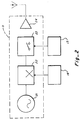
- the embodiment according to Figure 1 consists of a transmitter 11, a transponder 12 which e.g. could be a passive SAW transponder and a receiver 13 which is connected to an integrator arrangement 16 of integrator sections 37.
- a device 14 generates a binary random sequence which is passed to the transmitter 11 and a sieve register 17 which is connected to the integrator arrangement 16.
- a device 15 outputs a signal with time limits (time interval signal), which is fed to the transmitter 11 and the shift register 17.
- the transmitter 11 transmits a phase-modulated pulse sequence which is received and reflected by the encoded transponder 12, so that the reflected signal consists of series of pulse sequences and spaces without pulse sequences, which together form an identity which is identical to the transponder code.
- the desired signal is received by the receiver 13, which is then demodulated and sent to an integrator arrangement 16, which is controlled by the above-mentioned binary sequence from the submission 14 together with the temporal interruptions determined by the device 15.
- FIG. 2 shows a more detailed reproduction of the transmitter.
- This consists of an oscillator 21, which forms a fixed frequency signal.
- This fixed frequency signal is phase-modulated by the binary random sequence of the device 14.
- the signal modulated in the device 22 is divided into pulse sequences by means of a gate circuit 23 which is controlled by the time interval signal of the device 15.
- the pulse sequences are then amplified by an amplifier 24 before transmission.
- FIG 3 shows a more detailed representation of the receiver 13 and the decoder unit.
- the signal is demodulated in the receiver 13 into a time and phase-coded signal 31A, which is superimposed by unwanted noise.
- the signal 31A arrives at a switch 36A which directs the signal 31A into an integrator section 37 of the integrator arrangement 16.
- This integrator section 37 can e.g. be an RC filter with a large time constant compared to the individual signal run (e.g. 10000x larger).
- the binary sequence of the device 14 and the time interval signal of the device 15 form the input signals for an AND gate 32A, the output signal of which is fed to a shift register 33A, to which the same binary sequence as is used in the transmitter is then fed to form the phase-modulated pulse sequence .
- This binary sequence is clock driven by the shift register 33A using an external clock signal (not shown in the drawing). It is possible to obtain a signal from different positions in the shift register 33A, for example after certain time intervals after the output signal mentioned has been passed into the shift register 33A.
- the signal is removed from the shift register 33A and used to control the switch 36A, which opens or closes for forwarding the demodulated signal 31A from the receiver 13 to the integrator section 37.
- the signal 31A can be inverted by means of an inverter 34 to a signal 31B, which is also fed to the integrator section 37. This is achieved by passing the binary random sequence via an inverter 35 to a shift register 33B and removing it in a position corresponding to the first shift register 33A and controlling the switch 36B in such a way that it opens or closes for the inverted signal 31B in the integrator section 37.
- Both switches 36A and 36B can e.g. controlled such that a logic "1" in the binary sequence opens the switch for the non-inverted signal 31A from the receiver and closes the switch for the inverted signal 31B; if a logical "0" appears in the binary sequence, the opposite will happen.
- the AND gates 32A and 32B will always have a logic "0" at their output, which ensures is that both switches 36A and 36B are open to prevent undesired noise from being applied to integrator section 37.
- the integrator arrangement 16 is formed by a number of integrator sections 37, which are typically the same as the number of "bits” or a multiple of the number of "bits" of the transponder 12.
- the individual integrator sections 37 can be read out whenever the required number of pulse sequences has been processed. This reading can take place asynchronously, without previous events having to be given any attention.
- FIG. 4 shows in chronological representation how two pulse sequences are transmitted by the transmitter 11 and reflected by the transponder 12, in an embodiment in which the transponder 12 has a resolution of four "bits".
- the transponder 12 is encoded with the binary sequence (bit sequence) 1101.
- the first pulse sequence 41A is a phase-modulated signal which is modulated by the first part of a binary random sequence of the device 14, with a length which is determined by the time intervals formed by the device 15.
- the first pulse sequence 41A is received and reflected by the transponder 12, where it is coded for a logic "1". Because the transponder has code 1101 in this example, the reflected signal forms a pattern as shown at 41B where "bit 1", "bit 2" and "bit 4" reflect a pulse train while "bit 3", which has the value of logic "0" does not reflect a signal.
- the reflected pulse trains 41B can and will overlap in the various mutual positions without this having any negative consequences on the result.
- the second pulse train is sent.
- This pulse sequence is phase-modulated by another part of the binary random sequence, which is different from that in the first pulse sequence, and is activated by the device 14 for a certain period of time, which is determined by time interval signals coming from the device 15.
- This second pulse sequence 42A is then reflected by the transponder 12 as in the first case, so that a series of reflected pulse sequences 42B is formed.
- each phase-modulated, corresponding pulse train can be transmitted, reflected and fed to the integrator arrangement 16, so that the desired signal is averaged and most undesirable signals, which are random and asynchronous be reduced.
Abstract
Description
Die Erfindung betrifft ein Verfahren zum Behandeln von Signalen in einem Identifikationssystem, wie es in der Einleitung zu Patentanspruch 1 beschrieben ist.The invention relates to a method for handling signals in an identification system, as described in the introduction to
Die Erfindung ist vorgesehen für die Anwendung in einem Identifiktionssystem, welches aus einem Sender, einem mobilen, binär kodierten passiven, die Identifikation liefernden Antwortsendegerät (Transponder) und einer Empfängereinheit besteht, die in der Kombination ein Behandlungssystem darstellen.The invention is intended for use in an identification system, which consists of a transmitter, a mobile, binary-coded passive, the identification-providing answering device (transponder) and a receiver unit, which in combination form a treatment system.
Der Transponder kann mit Mitteln der SAW(Surface Acoustic Wave)-Technologie verwirklicht werden. Transponder nach dieser Technologie haben viele Vorteile für eine derartige Anwendung; sie sind nicht teuer, einfach herzustellen und erfordern keine Wartung, und sie sind unabhängig von äußeren Energiequellen usw. Jedoch hat ein Transpoder entsprechend dieser Technologie eine Charakteristik, die einen grundsätzlichen Nachteil hat: Die hohe Einfügungsdämpfung. Dies bedeutet, daß das reflektierte Rücksignal schwach ist im Verhältnis zum hereinkommenden Abfrageimpuls. Dieser Nachteil wird dadurch verstärkt, daß die Sendeeinheit ein schwaches Ausgangsradar benutzt, um den Abstrahlerfordernissen bei der benutzten Frequenz gerecht zu werden.The transponder can be implemented using SAW (Surface Acoustic Wave) technology. Transponders using this technology have many advantages for such an application; they are inexpensive, easy to manufacture and require no maintenance, and they are independent of external energy sources, etc. However, a transpoder according to this technology has a characteristic which has a fundamental disadvantage: the high insertion loss. This means that the reflected Return signal is weak in relation to the incoming interrogation pulse. This disadvantage is exacerbated by the fact that the transmitter unit uses a weak output radar in order to meet the radiation requirements for the frequency used.
Zusammenfassend ist das Resultat derart, daß die Stärke des erwünschten Rücksignals an die Empfängereinheit des Systems sehr gering ist im Verhältnis zu den unerwünschten Signalen, zum Rauschen und zum Eigenrauschen des Empfängers selbst.In summary, the result is such that the strength of the desired return signal to the receiver unit of the system is very small in relation to the unwanted signals, the noise and the self-noise of the receiver itself.
Das traditionelle Verfahren zum behandeln von Signalen zur Verbesserung des Signal/Rausch-Verhältnisses für die erwähnten Anwendungen besteht darin, das reflektierte Signal direkt mittels A/D(Analog/Digital)-Wandler zu digitalisieren und hieran eine digitale Verarbeitung anschließen zu lassen. Die Verarbeitung wird durchgeführt, indem die digitalen Werte der analogen Signale über mehrere wiederholte Rücksignaldurchläufe gemittelt werden. Dies verbessert das Signal/Rausch-Verhältnis, weil das erwünschte Signal in jedem Durchlauf gleich ist, während das Rauschen unterschiedlich ist. Andererseits erfordert dieses Verfahren eine leistungsstarke digitale Verarbeitungseinheit. Die Einheit muß schnell arbeiten und beträchtliche Rechenleistung aufweisen zum Mitteln einer entsprechenden Anzahl von Durchläufen. Gleichzeitig muß der A/D-Wandler eine der schnellsten und fortschrittlichsten Ausführungen sein, die erhältlich sind. Diese Lösung bedeutet, daß die angewendete Technologie klar Grenzen setzt dafür, wie effizient das Verfahren ist. Dies wird auch den Einsatz von teuren digitalen Prozessoren und A/D-Wandlern erfordern.The traditional method for treating signals to improve the signal-to-noise ratio for the applications mentioned is to digitize the reflected signal directly by means of A / D (analog / digital) converters and to have digital processing connected to it. Processing is performed by averaging the digital values of the analog signals over multiple repeated return signal passes. This improves the signal-to-noise ratio because the desired signal is the same in each pass, while the noise is different. On the other hand, this method requires a powerful digital processing unit. The unit must operate quickly and have significant computing power to average an appropriate number of passes. At the same time, the A / D converter must be one of the fastest and most advanced designs available. This solution means that the technology used clearly sets limits on how efficient the process is. This will also require the use of expensive digital processors and A / D converters.
Ein anderes in der Radar-Technologie eingesetzte Verfahren wendet Verzögerungsleitungen an, so daß ein Signal um einen Durchlauf verzögert wird und durch analoges Aufaddieren dieser Signale gemittelt wird. Dieses Verfahren weist eine Begrenzung auf, da die Anzahl der Mittelwertbildungen, die durchgeführt werden können, sehr eingeschränkt ist und es dort keine Synchronisation mit dem (Signal-)Durchlauf gibt.Another method used in radar technology uses delay lines so that a signal is delayed by one pass and averaged by adding these signals in an analog manner. This method has a limitation because the number of averages that can be carried out is very limited and there is no synchronization with the (signal) run.
Die US-Patentschrift 3 706 094 beschreibt einen Empfänger für ein Radar-Überwachungssystem mit niedriger Ausgangsleistung, bei dem der Empfänger ausgerüstet ist zum analogen Verarbeiten der empfangenen, zurücklaufenden Puls-Signale, von denen jedes Puls-Signal aufgeteilt wird durch eine bestimmte Anzahl von zeitlichen Unterbrechungen in gesteuerten Torschaltungen und bei dem das Signal von jeder Torschaltung einem Integrator zugeführt wird für die wiederholte Integration der Puls-Signale, wobei die Wiederholfrequenz der Puls-Signale beachtlich höher ist als die Grenz-Frequenz des Tiefpasses des Integrators. Das Puls-Signal kann durch Auslesen des Ausganges des Integrators vom Empfänger rekonstruiert werden.US Pat. No. 3,706,094 describes a receiver for a low output radar surveillance system, in which the receiver is equipped for analog processing of the received returning pulse signals, each of which is divided by a certain number of temporal signals Interruptions in controlled gate circuits and in which the signal from each gate circuit is fed to an integrator for the repeated integration of the pulse signals, the repetition frequency of the pulse signals being considerably higher than the limit frequency of the low-pass filter of the integrator. The pulse signal can be reconstructed by reading the output of the integrator from the receiver.
Das Hauptziel der vorliegenden Erfindung besteht darin, eine sichere Methode zu entwickeln zum Erkennen eines Radarsignals, welches von einem passiven, kodierten Transponder reflektiert wird unter Phasenmodulation des gesendeten Signals. - Dies kann durch Einsatz des Verfahrens nach Anspruch 1 erreicht werden. Andere Gesichtspunkte der Erfindung sind in den übrigen Patentansprüchen angegeben.The main aim of the present invention is to develop a safe method for recognizing a radar signal which is reflected by a passive, coded transponder with phase modulation of the transmitted signal. - This can be achieved by using the method according to
Die vorliegende Erfindung kann von der Technik nach der erwähnten Patentschrift durch die Tatsache unterschieden werden, daß die vorliegende Erfindung ein Zusammenwirken zwischen den gesendeten und reflektierten Signalen anwendet. Dies geschieht durch eine binäre, digitale Zufallssequenz, die das gesendete Signal moduliert, und Anwendung derselben Zufallssequenz zum Wiedererkennen des demodulierten, reflektierten Signals. Es wird eine große Anzahl von phasenmodulierten Pulsfolgen erzeugt, die vorzugsweise unterschiedlich sind. Dies wird erreicht durch Aufteilen der oben erwähnten binären Zufallssequenz und Benutzung dieser Aufteilungen der binären Zufallssequenz, um das demodulierte, reflektierte Signal einem Speichermedium zuzuführen wie einer Integratorkette, die derart beschaffen ist, daß das (Speicher-)Medium Werte entsprechen den erwünschten Signalen enthält, während unerwünschte Signale und Rauschen größtenteils reduziert werden.The present invention can be distinguished from the technique of the mentioned patent by the fact that the present invention employs a cooperation between the transmitted and reflected signals. This is done by means of a binary, digital random sequence that modulates the transmitted signal, and application of the same random sequence for recognizing the demodulated, reflected signal. A large number of phase-modulated pulse sequences are generated, which are preferably different. This is accomplished by splitting the binary random sequence mentioned above and using these splits of the binary random sequence to match the demodulated, reflected signal Feed storage medium such as an integrator chain, which is designed such that the (storage) medium contains values corresponding to the desired signals, while unwanted signals and noise are largely reduced.
Vorteile der Anwendung nach der Erfindung: Die im Rahmen der Erfindung angewendete Technik besteht aus einem analogen Mitteln (Mittelwertbildung) des Signals, bevor es digitalisiert wird.Advantages of the application according to the invention: The technology used in the context of the invention consists of analog averaging (averaging) of the signal before it is digitized.
Dies hat mehrere Vorteile gegenüber traditionellen Techniken. Es kann eine ungemein große Verarbeitungskapazität geschaffen werden nur durch Einsatz von herkömmlichen, kommerziell erhältlichen, kostengünstigen Komponenten. Daraus folgt eine Geschwindigkeit und Fähigkeit zur Mittelwertbildung für wiederholte Durchläufe, die weit hinausgehen über irgendwelche der oben erwähnten traditionellen Methoden. Gleichzeitig bedeutet die niedrigere Auswerterate, daß ein standardmäßiger, konventioneller Typ eines A/D-Wandlers und die darauf folgende digitale Verarbeitung eingesetzt werden kann, so daß dies kommerziell attraktiv ist.This has several advantages over traditional techniques. An extraordinarily large processing capacity can only be created by using conventional, commercially available, inexpensive components. This results in a speed and averaging ability for repeated runs that go far beyond any of the traditional methods mentioned above. At the same time, the lower evaluation rate means that a standard, conventional type of A / D converter and the subsequent digital processing can be used, so that this is commercially attractive.
Da eine binäre Sequenz sowohl beim Senden zum Modulieren des gesendeten Signals als auch für den Empfänger zum Steuern der Speicherung und Mittelwertbildung des demodulierten, reflektierten Signals benutzt wird, werden im Vergleich zu den erwünschten Signalen alle Arten von Rauschen und unerwünschten Signalen bedeutend reduziert. Weil die obige binäre Sequenz Teil einer binären Zufallssequenz ist, werden Rauschen und unerwünschte Signale sogar dann größtenteils reduziert, wenn sie Teil eines ungünstigen wiederholten Durchlaufes sind.Because a binary sequence is used both in transmission to modulate the transmitted signal and for the receiver to control the storage and averaging of the demodulated, reflected signal, all types of noise and unwanted signals are significantly reduced compared to the desired signals. Because the above binary sequence is part of a random binary sequence, noise and unwanted signals are largely reduced even if they are part of an unfavorable iterate.
Es ist auch möglich, das Senden zu verbessern durch Anwendung phasenmodulierter und vorzugsweise unterschiedlicher Pulsfolgen anstelle eines Einzelpulses, wobei die Länge einer Pulsfolge nach oben zu begrenzt ist durch die Dauer bis zum Eintreffen der ersten reflektierten Pulsfolge.It is also possible to improve the transmission by using phase-modulated and preferably different pulse sequences instead of a single pulse, the length of a pulse sequence being limited upwards by the duration until the arrival of the first reflected pulse sequence.
Im folgenden wird ein Ausführungsbeispiel der Erfindung unter Hinweis auf die Zeichnungen beschrieben.
Figur 1 zeigt eine Blockdarstellung einer Möglichkeit der Ausführung der Erfindung mit Einschluß der wesentlichen Komponenten,Figur 2 zeigt eine detailliertere Wiedergabe des Senders bei dieser besonderen Ausführungsform,Figur 3 zeigt eine detailliertere Wiedergabe des Empfängers und der Dekodereinheit bei dieser besonderen Ausführungsform, undFigur 4 zeigt eine chronologische Wiedergabe der gesendeten und reflektierten Signale im Fall dieser Ausführungsform der Erfindung.
- FIG. 1 shows a block diagram of one possible embodiment of the invention, including the essential components,
- FIG. 2 shows a more detailed reproduction of the transmitter in this particular embodiment,
- Figure 3 shows a more detailed representation of the receiver and decoder unit in this particular embodiment, and
- Figure 4 shows a chronological representation of the transmitted and reflected signals in the case of this embodiment of the invention.
Die Ausführungsform nach Figur 1 besteht aus einem Sender 11, einem Transponder 12, der z.B. ein passiver SAW-Transponder sein könnte, und einem Empfänger 13, der mit einer Integratoranordnung 16 von Integratorabschnitten 37 verbunden ist. Eine Einrichtung 14 erzeugt eine binäre Zufallssequenz, die zu dem Sender 11 und einem Sieberegister 17 geleitet wird, welches mit der Integratoranordnung 16 verbunden ist. Eine Einrichtung 15 gibt ein Signal mit zeitlichen Begrenzungen (Zeitintervallsignal), welches dem Sender 11 und dem Schieberegister 17 zugeführt wird.The embodiment according to Figure 1 consists of a transmitter 11, a transponder 12 which e.g. could be a passive SAW transponder and a
Der Sender 11 sendet eine phasenmodulierte Pulsfolge, die von dem kodierten Transponder 12 empfangen und reflektiert wird, so daß das reflektierte Signal aus Serien von Pulsfolgen und Zwischenräumen ohne Pulsfolgen besteht, welche zusammen eine Identität bilden, die dem Transpondercode gleicht. Das erwünschte Signal wird von dem Empfänger 13 aufgenommen, der es dann demoduliert und an eine Integratoranordnung 16 gibt, die von der oben erwähnten binären Sequenz von der Einreichung 14 her gesteuert wird zusammen mit den zeitlichen, von der Einrichtung 15 bestimmten Unterbrechungen.The transmitter 11 transmits a phase-modulated pulse sequence which is received and reflected by the encoded transponder 12, so that the reflected signal consists of series of pulse sequences and spaces without pulse sequences, which together form an identity which is identical to the transponder code. The The desired signal is received by the
Figur 2 gibt eine detailliertere Wiedergabe des Senders wieder. Dieser besteht aus einem Oszillator 21, der ein Festfrequenzsignal bildet. Dieses Festfrequenzsignal wird phasenmoduliert durch die binäre Zufallssequenz der Einrichtung 14. Das in der Einrichtung 22 modulierte das Signal wird in Pulsfolgen aufgeteilt mittels einer Torschaltung 23, die von dem Zeitintervallsignal der Einrichtung 15 gesteuert wird. Die Pulsfolgen werden dann vor dem Senden von einem Verstärker 24 verstärkt.Figure 2 shows a more detailed reproduction of the transmitter. This consists of an
Figur 3 zeigt eine detailliertere Wiedergabe des Empfängers 13 und der Dekodereinheit. Das Signal wird im Empfänger 13 in ein zeit- und phasen-kodiertes Signal 31A demoduliert, welches überlagert ist von unerwünschtem Rauschen. In diesem Beispiel der Erfindung gelangt das Signal 31A zu einem Schalter 36A, der das Signal 31A in einen Integratorabschnitt 37 der Integratoranordnung 16 leitet. Dieser Integratorabschnitt 37 kann z.B. ein RC-Filter sein mit einer großen Zeitkonstante, verglichen mit dem individuellen Signaldurchlauf (z.B. 10000x größer).Figure 3 shows a more detailed representation of the
Die binäre Sequenz der Einrichtung 14 und das Zeitintervallsignal der Einrichtung 15 bilden die Eingangssignale für ein UND-Gatter 32A, dessen Ausgangssignal zu einem Schieberegister 33A geführt wird, dem dann dieselbe binäre Sequenz zugeführt wird, wie sie im Sender benutzt wird zum Bilden der phasenmodulierten Pulsfolge. Diese binäre Sequenz wird taktgesteuert durch das Schieberegister 33A bewegt unter Verwendung eines äußeren Taktsignals (in der Zeichnung nicht dargestellt). Es ist möglich, ein Signal von verschiedenen Positionen im Schieberegister 33A zu erhalten, z.B. nach bestimmten Zeitintervallen, nachdem das erwähnte Ausgangssignal in das Schieberegister 33A geleitet worden ist. Wenn der Zeitraum verstrichen ist, der der Zeitverzögerung für die erste vom Transponder 12 reflektierte Pulsfolge gleicht, wird das Signal aus dem Schieberegister 33A entfernt und zur Steuerung des Schalters 36A benutzt, welcher für die Weiterleitung des demodulierten Signals 31A vom Empfänger 13 in den Integratorabschnitt 37 öffnet oder schließt.The binary sequence of the
Das Signal 31A kann mittels eines Inverters 34 invertiert werden zu einem Signal 31B, welches ebenfalls zum Integratorabschnitt 37 geführt wird. Dies wird erreicht durch Leiten der binären Zufallssequenz über einen Inverter 35 zu einem Schieberegister 33B und seiner Entnahme in einer dem ersten Schieberegister 33A entsprechenden Position und Steuerung des Schalters 36B derart, daß dieser für das invertierte Signal 31B in den Integratorabschnitt 37 öffnet oder schließt. Beide Schalter 36A und 36B können z.B. derart gesteuert werden, daß eine logische "1" in der binären Sequenz den Schalter für das nicht-invertierte Signal 31A vom Empfänger öffnet und der Schalter für das invertierte Signal 31B schließt; wenn eine logische "0" in der binären Sequenz erscheint, wird das Gegenteilige geschehen.The
In dem Zeitraum, während dessen vom Sender 11 keine Pulsfolgen gesendet werden, weil das Signal der Einrichtung 15 den Wert einer logischen "0" hat, werden die UND-Gatter 32A und 32B immer einer logische "0" an ihrem Ausgang haben, womit sichergestellt ist, daß beide Schalter 36A und 36B offen sind zum Verhindern der Einwirkung von unerwünschtem Rauschen auf den Integratorabschnitt 37.During the period during which the transmitter 11 does not send any pulse trains because the signal of the
Die Integratoranordnung 16 wird gebildet von einer Anzahl von Integratorabschnitten 37, die typischerweise der Anzahl der "Bits" oder des Mehrfachen der Anzahl der "Bits" des Transponders 12 gleichen. Die individuellen Integratorabschnitte 37 können immer dann ausgelesen werden, wenn die erforderliche Anzahl von Pulsfolgen verarbeitet worden ist. Dieses Auslesen kann asynchron erfolgen, ohne daß vorangegangenen Geschehnissen irgendeine Beachtung geschenkt werden muß.The
Figur 4 zeigt in chronologischer Wiedergabe, wie zwei Pulsfolgen vom Sender 11 gesendet und vom Transponder 12 reflektiert werden, in einer Ausführungsform, bei der der Transponder 12 eine Auflösung von vier "Bits" hat. Hier ist der Transponder 12 mit der binären Sequenz (Bitsequenz) 1101 kodiert.FIG. 4 shows in chronological representation how two pulse sequences are transmitted by the transmitter 11 and reflected by the transponder 12, in an embodiment in which the transponder 12 has a resolution of four "bits". Here, the transponder 12 is encoded with the binary sequence (bit sequence) 1101.
Die erste Pulsfolge 41A ist ein phasenmoduliertes Signal, welches durch den ersten Teil einer binären Zufallssequenz der Einrichtung 14 moduliert ist, mit einer Länge, welche durch die von der Einrichtung 15 gebildeten Zeitintervalle bestimmt ist. Die erste Pulsfolge 41A wird vom Transponder 12 empfangen und reflektiert, wo dieser für eine logische "1" kodiert ist. Da der Transponder in diesem Beispiel den Kode 1101 hat, bildet das reflektierte Signal ein Muster, wie es bei 41B gezeigt ist, wo "Bit 1", "Bit 2" und "Bit 4" eine Pulsfolge reflektieren, während "Bit 3", welches den Wert der logischen "0" hat, kein Signal reflektiert. Die reflektierten Pulsfolgen 41B können und werden sich in den verschiedenen gegenseitigen Positionen überlappen, ohne daß dies irgendwelche negativen Konsequenzen auf das Resultat hätte.The first pulse sequence 41A is a phase-modulated signal which is modulated by the first part of a binary random sequence of the
Sobald die letzte reflektierte Pulsfolge empfangen worden ist, wird die zweite Pulsfolge gesendet. Diese Pulsfolge wird von einem anderen Teil der binären Zufallssequenz phasenmoduliert, die unterschiedlich zu der in der ersten Pulsfolge ist, und von der Einrichtung 14 aktiviert ist für eine bestimmte Zeitdauer, die durch von der Einrichtung 15 kommende Zeitintervallsignale bestimmt wird. Diese zweite Pulsfolge 42A wird dann wie im ersten Fall vom Transponder 12 reflektiert, so daß eine Reihe reflektierter Pulsfolgen 42B gebildet ist.As soon as the last reflected pulse train has been received, the second pulse train is sent. This pulse sequence is phase-modulated by another part of the binary random sequence, which is different from that in the first pulse sequence, and is activated by the
Es kann eine große Anzahl von den Pulsfolgen 41a und 42A, jeweils auf unterschiedliche Weise phasenmodulierten, entsprechenden Pulsfolgen gesendet, reflektiert und zu der Integratoranordnung 16 geführt werden, so daß das gewünschte Signal gemittelt wird und unerwünschte Signale, die zufälliger Natur und asynchron sind, größtenteils reduziert werden.A large number of the pulse trains 41a and 42A, each phase-modulated, corresponding pulse train can be transmitted, reflected and fed to the
Claims (11)
- Method of processing signals in an identification system, in which:a) a radar signal is transmitted from a transmitter,b) the radar signal is received by a mobile transponder,c) the transponder sends back a binary-coded signal, andd) the signal sent back by the transponder is received by a receiver and is processed in order to separate unwanted signals and noise from the wanted, binary-coded return signals,characterised in that, in order to improve the processing quality, capacity and speede) the electrical signal for transmission as a radar signal is phase-modulated by the application of a binary pseudo-random sequence,f) the phase-modulated electrical signal is divided up, with the formation of signal-free time intervals, and the pulse sequences (41A, 42A) thus formed are transmitted as a radar signal,g) transmitted pulse sequences (41A, 42A) of the radar signal from the transponder are passively reflected in accordance with its binary coding,h) the pulse sequences (41B, 42B) reflected by the transponder are received and demodulated and the same binary pseudo-random sequence and the same time intervals as are applied in transmitting, both time-delayed, are used for storing and forming an average value and processing the identification of the transponder for the purpose of individual identification, andi) the signals obtained from the demodulation of the reflected pulse sequences (41B, 42B) are fed to a storage medium in such a manner that the discrete values of the delayed binary pseudo-random sequence operate a device (36) which opens the storage medium to pulse sequence signals with a specified binary value and which closes the storage medium to pulse sequence signals having the inverse value thereto.
- Method according to claim 1, characterised in that the pulse sequence is preferably different for each repeated cycle.
- Method according to claim 1, characterised in that the transponder (12) reflects the pulse sequences (41B, 42B) at different instants due to different binary codings of the transponder (12).
- Method according to claim 1, characterised in that the binary random sequence is fed to a device (17) which temporally delays their values in such a manner that they are synchronised with the reflected, received and demodulated pulse sequence (31A, 31B).
- Method according to claim 4, characterised in that signals corresponding to the time intervals and the pseudo-random sequence, before being delayed, pass through a logical AND-operation.
- Method according to claim 1, characterised in that the signals obtained from demodulation of the reflected pulse sequences (41B, 42B) are inverted (31B) and are fed to the storage medium, operated in an inverse manner by the values of the aforesaid part of the delayed binary random sequence.
- Method according to claim 1, characterised in that storage is carried out with a storage medium in which a number of values can be stored, which number is determined by the number of bits of the transponder (12) or for a multiple of that number or bits.
- Method according to claim 7, characterised in that the signals corresponding to the pseudo-random sequence and the time intervals are temporally delayed and are applied at different instants in order to operate the storage medium according to the coding in the transponder or to a multiple of these time delays.
- Method according to claim 1, characterised in that the storage medium is such that repeated cycles of the received, demodulated and stored pulse sequences are averaged.
- Device for carrying out the method according to the preceding claims for treating signals in an identification system, comprisinga) a transmitter (11) for transmitting a radar signal and comprising an oscillator (21),b) a binary-coded, mobile transponder (12) for reflecting the radar signal, andc) a receiver (13) for receiving and demodulating the reflected radar signal,
characterised in thatd) the transmitter (11) is connected not only to a phase-modulating device (22), but also to a device (14) for generating a binary random sequence,e) the transmitter (11) is further connected to a device (15) for dividing up the phase-modulated signal of the transmitter (11) into pulse sequences (41A, 41B) with the formation of signal-free time intervals,f) the transponder (12) is individually binary-coded for passively reflecting pulse sequences (41B, 42B) having this code, andg) on the receiving side, the device (14) for generating the binary random sequence and the device (15) for dividing up the phase-modulated signal into pulse sequences are respectively connected to at least one AND-gate (32) and by a respective output to at least one shift register (33) for controlling an adjustable integrator circuit (16) connected to a receiver (13) and acting as a storage medium. - Device according to claim 10, characterised in that an inverter (34) is provided for the demodulated radar signal and a further inverter (35) is provided for the time interval signal, supplied to a second shift register (33B), for guiding the demodulated and inverted radar signal into the storage medium.
Applications Claiming Priority (3)
| Application Number | Priority Date | Filing Date | Title |
|---|---|---|---|
| NO884784A NO169983C (en) | 1988-10-27 | 1988-10-27 | PROCEDURE AND DEVICE FOR INDIVIDUAL IDENTIFICATION |
| NO884784 | 1988-10-27 | ||
| PCT/NO1989/000034 WO1990004794A1 (en) | 1988-10-27 | 1989-04-24 | Method for processing transmitted and reflected signals for removing unwanted signals and noise from wanted signals |
Publications (2)
| Publication Number | Publication Date |
|---|---|
| EP0440624A1 EP0440624A1 (en) | 1991-08-14 |
| EP0440624B1 true EP0440624B1 (en) | 1996-01-24 |
Family
ID=19891368
Family Applications (1)
| Application Number | Title | Priority Date | Filing Date |
|---|---|---|---|
| EP89904622A Expired - Lifetime EP0440624B1 (en) | 1988-10-27 | 1989-04-24 | Method for processing transmitted and reflected signals for removing unwanted signals and noise from wanted signals |
Country Status (12)
| Country | Link |
|---|---|
| US (1) | US5144313A (en) |
| EP (1) | EP0440624B1 (en) |
| JP (1) | JPH04502059A (en) |
| AT (1) | ATE133496T1 (en) |
| AU (1) | AU625991B2 (en) |
| CA (1) | CA1337829C (en) |
| DE (1) | DE58909583D1 (en) |
| DK (1) | DK74891A (en) |
| ES (1) | ES2016047A6 (en) |
| FI (1) | FI102418B1 (en) |
| NO (1) | NO169983C (en) |
| WO (1) | WO1990004794A1 (en) |
Families Citing this family (32)
| Publication number | Priority date | Publication date | Assignee | Title |
|---|---|---|---|---|
| US5231400A (en) * | 1992-05-12 | 1993-07-27 | Unisys Corporation | Covert electronic battlefield identification system |
| US5500650A (en) * | 1992-12-15 | 1996-03-19 | Micron Technology, Inc. | Data communication method using identification protocol |
| US5365551A (en) * | 1992-12-15 | 1994-11-15 | Micron Technology, Inc. | Data communication transceiver using identification protocol |
| US7158031B2 (en) | 1992-08-12 | 2007-01-02 | Micron Technology, Inc. | Thin, flexible, RFID label and system for use |
| US5557280A (en) * | 1992-08-26 | 1996-09-17 | British Technology Group Limited | Synchronized electronic identification system |
| US20050040961A1 (en) * | 1995-04-11 | 2005-02-24 | Tuttle John R. | RF identification system with restricted range |
| US6097301A (en) * | 1996-04-04 | 2000-08-01 | Micron Communications, Inc. | RF identification system with restricted range |
| US5349355A (en) * | 1993-01-21 | 1994-09-20 | The United States Of America As Represented By The Secretary Of The Navy | Credential tracking system |
| JP3147306B2 (en) * | 1996-10-17 | 2001-03-19 | ピンポイント コーポレイション | Item tracking system |
| US6812824B1 (en) | 1996-10-17 | 2004-11-02 | Rf Technologies, Inc. | Method and apparatus combining a tracking system and a wireless communication system |
| US6107910A (en) | 1996-11-29 | 2000-08-22 | X-Cyte, Inc. | Dual mode transmitter/receiver and decoder for RF transponder tags |
| US6208062B1 (en) | 1997-08-18 | 2001-03-27 | X-Cyte, Inc. | Surface acoustic wave transponder configuration |
| US5986382A (en) | 1997-08-18 | 1999-11-16 | X-Cyte, Inc. | Surface acoustic wave transponder configuration |
| US6114971A (en) | 1997-08-18 | 2000-09-05 | X-Cyte, Inc. | Frequency hopping spread spectrum passive acoustic wave identification device |
| US6060815A (en) | 1997-08-18 | 2000-05-09 | X-Cyte, Inc. | Frequency mixing passive transponder |
| US6339385B1 (en) | 1997-08-20 | 2002-01-15 | Micron Technology, Inc. | Electronic communication devices, methods of forming electrical communication devices, and communication methods |
| US6118789A (en) | 1998-02-19 | 2000-09-12 | Micron Technology, Inc. | Method of addressing messages and communications system |
| US6275476B1 (en) | 1998-02-19 | 2001-08-14 | Micron Technology, Inc. | Method of addressing messages and communications system |
| US6072801A (en) | 1998-02-19 | 2000-06-06 | Micron Technology, Inc. | Method of addressing messages, method of establishing wireless communications, and communications system |
| USRE43382E1 (en) | 1998-02-19 | 2012-05-15 | Round Rock Research, Llc | Method of addressing messages and communications systems |
| US6061344A (en) | 1998-02-19 | 2000-05-09 | Micron Technology, Inc. | Method of addressing messages and communications system |
| US6714121B1 (en) * | 1999-08-09 | 2004-03-30 | Micron Technology, Inc. | RFID material tracking method and apparatus |
| US7054348B2 (en) * | 2001-11-15 | 2006-05-30 | Koninklijke Philips Electronic N.V. | Using real random number generator as proof of time |
| US7298264B1 (en) | 2004-01-20 | 2007-11-20 | Charles A. Eldering | RFID tag filtering and monitoring |
| US7420458B1 (en) | 2004-01-20 | 2008-09-02 | Charles A. Eldering | Secondary card reader |
| US20080109502A1 (en) * | 2004-09-30 | 2008-05-08 | Benjamin Aaron Gittins | Method And Apparatus For Partitioning Of A Bitstream |
| US7973644B2 (en) * | 2007-01-30 | 2011-07-05 | Round Rock Research, Llc | Systems and methods for RFID tag arbitration where RFID tags generate multiple random numbers for different arbitration sessions |
| US20080212303A1 (en) * | 2007-03-02 | 2008-09-04 | Warren Farnworth | Device for reducing or preventing exchange of information |
| US8134452B2 (en) * | 2007-05-30 | 2012-03-13 | Round Rock Research, Llc | Methods and systems of receiving data payload of RFID tags |
| WO2012055148A1 (en) * | 2010-10-27 | 2012-05-03 | 中国人民解放军第四军医大学 | Multichannel ultra wide band based (uwb-based) radar life detector and positioning method thereof |
| US8576114B2 (en) * | 2011-06-24 | 2013-11-05 | Thales Canada Inc. | Location of a transponder center point |
| CN112098927B (en) * | 2020-08-19 | 2022-06-21 | 中国电子科技集团公司第二十九研究所 | Multi-channel direction finding method based on signal synthesis |
Family Cites Families (7)
| Publication number | Priority date | Publication date | Assignee | Title |
|---|---|---|---|---|
| US3663935A (en) * | 1967-06-05 | 1972-05-16 | Hughes Aircraft Co | Pulse compression code sequencing system |
| US3691557A (en) * | 1969-09-22 | 1972-09-12 | James Nickolas Constant | System for identifying objects using an encoding array for each object |
| US3706094A (en) * | 1970-02-26 | 1972-12-12 | Peter Harold Cole | Electronic surveillance system |
| FR2248517B1 (en) * | 1973-10-23 | 1978-08-04 | Sercel Rech Const Elect | |
| GB1605271A (en) * | 1975-04-03 | 1987-06-10 | Secr Defence | Radio signalling equipment |
| US4015259A (en) * | 1975-05-21 | 1977-03-29 | The United States Of America As Represented By The Secretary Of The Army | Method and apparatus for interrogating and identifying fixed or moving targets |
| US4725841A (en) * | 1983-06-30 | 1988-02-16 | X-Cyte, Inc. | System for interrogating a passive transponder carrying phase-encoded information |
-
1988
- 1988-10-27 NO NO884784A patent/NO169983C/en not_active IP Right Cessation
-
1989
- 1989-04-24 AT AT89904622T patent/ATE133496T1/en not_active IP Right Cessation
- 1989-04-24 DE DE58909583T patent/DE58909583D1/en not_active Expired - Fee Related
- 1989-04-24 AU AU34185/89A patent/AU625991B2/en not_active Ceased
- 1989-04-24 WO PCT/NO1989/000034 patent/WO1990004794A1/en active IP Right Grant
- 1989-04-24 EP EP89904622A patent/EP0440624B1/en not_active Expired - Lifetime
- 1989-04-24 JP JP1504213A patent/JPH04502059A/en active Pending
- 1989-06-15 CA CA000602914A patent/CA1337829C/en not_active Expired - Lifetime
- 1989-07-27 ES ES8902660A patent/ES2016047A6/en not_active Expired - Fee Related
-
1991
- 1991-04-23 DK DK074891A patent/DK74891A/en not_active Application Discontinuation
- 1991-04-24 US US07/690,498 patent/US5144313A/en not_active Expired - Lifetime
- 1991-04-29 FI FI912068A patent/FI102418B1/en not_active IP Right Cessation
Also Published As
| Publication number | Publication date |
|---|---|
| FI102418B (en) | 1998-11-30 |
| DK74891D0 (en) | 1991-04-23 |
| FI102418B1 (en) | 1998-11-30 |
| DK74891A (en) | 1991-06-25 |
| AU3418589A (en) | 1990-05-14 |
| NO884784L (en) | 1990-04-30 |
| WO1990004794A1 (en) | 1990-05-03 |
| ES2016047A6 (en) | 1990-10-01 |
| JPH04502059A (en) | 1992-04-09 |
| NO169983C (en) | 1992-08-26 |
| AU625991B2 (en) | 1992-07-23 |
| ATE133496T1 (en) | 1996-02-15 |
| EP0440624A1 (en) | 1991-08-14 |
| FI912068A0 (en) | 1991-04-29 |
| DE58909583D1 (en) | 1996-03-07 |
| NO169983B (en) | 1992-05-18 |
| CA1337829C (en) | 1995-12-26 |
| US5144313A (en) | 1992-09-01 |
| NO884784D0 (en) | 1988-10-27 |
Similar Documents
| Publication | Publication Date | Title |
|---|---|---|
| EP0440624B1 (en) | Method for processing transmitted and reflected signals for removing unwanted signals and noise from wanted signals | |
| DE2347146A1 (en) | METHOD AND ARRANGEMENT FOR ULTRASONIC MESSAGE TRANSMISSION | |
| DE3116562A1 (en) | DOPPLERRADAR SYSTEM | |
| DE2801468A1 (en) | DECODING CIRCUIT FOR DIGITAL SIGNALS | |
| DE3047942C2 (en) | ||
| DE2403098A1 (en) | SYSTEM FOR TRANSMITTING COLUMN-PHASE MANCHESTER-CODED TWO-VALUE DATA SIGNALS | |
| DE2459885C2 (en) | Circuit for decoding a dynamically modulated signal | |
| DE4308241A1 (en) | ||
| DE1562052B2 (en) | RE-CODE THE MESSAGE TRANSFER SYSTEM WITH SEND AND RECEIVE SIDES | |
| DE1437511B2 (en) | ||
| DE2556625A1 (en) | ARRANGEMENT FOR IDENTIFICATION OF OBJECTS EQUIPPED WITH ANSWERBAKE | |
| DE1905680C3 (en) | Arrangement for changing the duration of frequency-modulated pulses, especially when using pulse compression, the ultrasonic retroreflective detection systems work | |
| DE4001265C2 (en) | Method and device for receiving digital information via power supply networks | |
| DE2326985A1 (en) | DEVICE FOR USING THE FREQUENCY OF AN ELECTRICAL SIGNAL OF SHORT DURATION | |
| DE1934869B2 (en) | PROCEDURE AND CIRCUIT ARRANGEMENT FOR CODING ASYNCHRONOUS BINARY DIGITAL SIGNALS | |
| DE2052845A1 (en) | Data transmission method with partially overlapping signals | |
| DE2300762C3 (en) | Arrangement for the recovery of the information from an encoded message | |
| DE2450289A1 (en) | PERSONAL PAGE SYSTEM | |
| DE2903329C2 (en) | Arrangement for coding binary data | |
| DE2628907C2 (en) | Process for the simultaneous transmission of a main pulse and two auxiliary pulsations derived from it | |
| DE2456178A1 (en) | CIRCUIT ARRANGEMENT FOR AN AUTOMATIC GAIN CONTROL FOR CODED DATA | |
| DE2331591C3 (en) | Procedure for the transmission of underwater signals | |
| AT269226B (en) | Method and arrangement for the transmission of digital data | |
| DE2039404B2 (en) | IN THE LOST PULSE PAIRS, FILLING PULSE PAIRS OF EMISSING TRANSPONDER WITH HIGH RESPONSE EFFICIENCY | |
| DE2060455C3 (en) | Method for transmitting commands to a missile or satellite that can be controlled remotely by radio and a command transmission system for carrying out this method |
Legal Events
| Date | Code | Title | Description |
|---|---|---|---|
| PUAI | Public reference made under article 153(3) epc to a published international application that has entered the european phase |
Free format text: ORIGINAL CODE: 0009012 |
|
| 17P | Request for examination filed |
Effective date: 19910427 |
|
| AK | Designated contracting states |
Kind code of ref document: A1 Designated state(s): AT BE CH DE FR GB IT LI LU NL SE |
|
| 17Q | First examination report despatched |
Effective date: 19930713 |
|
| GRAA | (expected) grant |
Free format text: ORIGINAL CODE: 0009210 |
|
| AK | Designated contracting states |
Kind code of ref document: B1 Designated state(s): AT BE CH DE FR GB IT LI LU NL SE |
|
| PG25 | Lapsed in a contracting state [announced via postgrant information from national office to epo] |
Ref country code: IT Free format text: LAPSE BECAUSE OF FAILURE TO SUBMIT A TRANSLATION OF THE DESCRIPTION OR TO PAY THE FEE WITHIN THE PRE;WARNING: LAPSES OF ITALIAN PATENTS WITH EFFECTIVE DATE BEFORE 2007 MAY HAVE OCCURRED AT ANY TIME BEFORE 2007. THE CORRECT EFFECTIVE DATE MAY BE DIFFERENT FROM THE ONE RECORDED.SCRIBED TIME-LIMIT Effective date: 19960124 Ref country code: BE Effective date: 19960124 Ref country code: NL Free format text: LAPSE BECAUSE OF FAILURE TO SUBMIT A TRANSLATION OF THE DESCRIPTION OR TO PAY THE FEE WITHIN THE PRESCRIBED TIME-LIMIT Effective date: 19960124 |
|
| REF | Corresponds to: |
Ref document number: 133496 Country of ref document: AT Date of ref document: 19960215 Kind code of ref document: T |
|
| REF | Corresponds to: |
Ref document number: 58909583 Country of ref document: DE Date of ref document: 19960307 |
|
| GBT | Gb: translation of ep patent filed (gb section 77(6)(a)/1977) |
Effective date: 19960307 |
|
| PG25 | Lapsed in a contracting state [announced via postgrant information from national office to epo] |
Ref country code: SE Effective date: 19960424 |
|
| ET | Fr: translation filed | ||
| PG25 | Lapsed in a contracting state [announced via postgrant information from national office to epo] |
Ref country code: LU Free format text: LAPSE BECAUSE OF NON-PAYMENT OF DUE FEES Effective date: 19960430 Ref country code: LI Effective date: 19960430 Ref country code: CH Effective date: 19960430 |
|
| NLV1 | Nl: lapsed or annulled due to failure to fulfill the requirements of art. 29p and 29m of the patents act | ||
| PLBE | No opposition filed within time limit |
Free format text: ORIGINAL CODE: 0009261 |
|
| STAA | Information on the status of an ep patent application or granted ep patent |
Free format text: STATUS: NO OPPOSITION FILED WITHIN TIME LIMIT |
|
| REG | Reference to a national code |
Ref country code: CH Ref legal event code: PL |
|
| 26N | No opposition filed | ||
| REG | Reference to a national code |
Ref country code: GB Ref legal event code: IF02 |
|
| PGFP | Annual fee paid to national office [announced via postgrant information from national office to epo] |
Ref country code: GB Payment date: 20040331 Year of fee payment: 16 |
|
| PGFP | Annual fee paid to national office [announced via postgrant information from national office to epo] |
Ref country code: AT Payment date: 20040405 Year of fee payment: 16 |
|
| PGFP | Annual fee paid to national office [announced via postgrant information from national office to epo] |
Ref country code: DE Payment date: 20040408 Year of fee payment: 16 |
|
| PGFP | Annual fee paid to national office [announced via postgrant information from national office to epo] |
Ref country code: FR Payment date: 20040415 Year of fee payment: 16 |
|
| PG25 | Lapsed in a contracting state [announced via postgrant information from national office to epo] |
Ref country code: GB Free format text: LAPSE BECAUSE OF NON-PAYMENT OF DUE FEES Effective date: 20050424 Ref country code: AT Free format text: LAPSE BECAUSE OF NON-PAYMENT OF DUE FEES Effective date: 20050424 |
|
| PG25 | Lapsed in a contracting state [announced via postgrant information from national office to epo] |
Ref country code: DE Free format text: LAPSE BECAUSE OF NON-PAYMENT OF DUE FEES Effective date: 20051101 |
|
| GBPC | Gb: european patent ceased through non-payment of renewal fee |
Effective date: 20050424 |
|
| PG25 | Lapsed in a contracting state [announced via postgrant information from national office to epo] |
Ref country code: FR Free format text: LAPSE BECAUSE OF NON-PAYMENT OF DUE FEES Effective date: 20051230 |
|
| REG | Reference to a national code |
Ref country code: FR Ref legal event code: ST Effective date: 20051230 |