EP0439807B1 - Système de communication à modulation par décalage de code - Google Patents
Système de communication à modulation par décalage de code Download PDFInfo
- Publication number
- EP0439807B1 EP0439807B1 EP90125190A EP90125190A EP0439807B1 EP 0439807 B1 EP0439807 B1 EP 0439807B1 EP 90125190 A EP90125190 A EP 90125190A EP 90125190 A EP90125190 A EP 90125190A EP 0439807 B1 EP0439807 B1 EP 0439807B1
- Authority
- EP
- European Patent Office
- Prior art keywords
- subinterval
- peaks
- denotes
- signal
- peak
- Prior art date
- Legal status (The legal status is an assumption and is not a legal conclusion. Google has not performed a legal analysis and makes no representation as to the accuracy of the status listed.)
- Expired - Lifetime
Links
Images


Classifications
-
- H—ELECTRICITY
- H04—ELECTRIC COMMUNICATION TECHNIQUE
- H04B—TRANSMISSION
- H04B1/00—Details of transmission systems, not covered by a single one of groups H04B3/00 - H04B13/00; Details of transmission systems not characterised by the medium used for transmission
- H04B1/69—Spread spectrum techniques
- H04B1/707—Spread spectrum techniques using direct sequence modulation
- H04B1/709—Correlator structure
-
- H—ELECTRICITY
- H04—ELECTRIC COMMUNICATION TECHNIQUE
- H04B—TRANSMISSION
- H04B1/00—Details of transmission systems, not covered by a single one of groups H04B3/00 - H04B13/00; Details of transmission systems not characterised by the medium used for transmission
- H04B1/69—Spread spectrum techniques
- H04B1/707—Spread spectrum techniques using direct sequence modulation
-
- H—ELECTRICITY
- H04—ELECTRIC COMMUNICATION TECHNIQUE
- H04J—MULTIPLEX COMMUNICATION
- H04J13/00—Code division multiplex systems
- H04J13/0074—Code shifting or hopping
-
- H—ELECTRICITY
- H04—ELECTRIC COMMUNICATION TECHNIQUE
- H04L—TRANSMISSION OF DIGITAL INFORMATION, e.g. TELEGRAPHIC COMMUNICATION
- H04L23/00—Apparatus or local circuits for systems other than those covered by groups H04L15/00 - H04L21/00
- H04L23/02—Apparatus or local circuits for systems other than those covered by groups H04L15/00 - H04L21/00 adapted for orthogonal signalling
Definitions
- the invention relates to a Code Shift-Keying (CSK) communication system receiver and receiving method.
- CSK Code Shift-Keying
- SS Spread Spectrum
- FIG. 1(a) A block diagram of one conventional SS communication System is shown in Figure 1(a). Timing of the signals associated with Figure 1(a) is shown by Figure 1(b).
- the PN cods T10 from a pseudo noise (PN) code generator 10 and data stream i20 are processed by the EX-OR gate 20. Its output signal T20 is amplified by 30, and then processed for transmission. After the transmitted signal T30 is received, it is amplified by an amplifier 40, whose output is applied to a correlator 50.
- the signal T50 from the correlator 50 is compared to a threshold value TH1 by a comparator 70, which produces demodulated data T70.
- the PN code generated by correlator 50 at the receiver must be synchronized to the PN code T10 modulated on the transmitted signal T30.
- the transmitted signal T30 experiences progressive deterioration, the output of the correlator 50 will lose its synchronization (loss of lock).
- Figure 2 illustrates a general block diagram of such CSK spread spectrum communication system consisting of a transmitter 200 and a receiver 270.
- the transmitter includes a modulator 280, which in turn comprises the following elements.
- the output from the modulator 280 is further processed and transmitted at the signal transmitting interface 240.
- the transmitted signal T240 is then later recaptured at a signal receiving interface 250, where PN modulated signal T250 is recovered from the received signal T240.
- the recovered signal T250 is input to the demodulator/correlator 260, where T250 is correlated with local copies of the PN codes and demodulated to recover the transmitted bits i230.
- a conventional PN communication system is likely to lose lock in cases where the communication "channel" (transmission path) introduce, significant amount of signal degradation.
- Implementations of the CSK system as originally proposed by the inventors overcomes the difficulty suffered by the conventional spread spectrum systems. However, the previously proposed implementation of the CSK system is still not perfect.
- the signal receiving interface 250 in the CSK system above transfers its output to a pair of correlators (not shown).
- One of two correlators multiplies the incoming signal by a local copy of M00.
- the other correlator by M01.
- one of two correlation signals at the output of correlators will have an auto-correlation peak, and the other will contain only cross-correlation peaks.
- signal demodulation depends on the detection of auto-correlation peaks, large cross-correlation peaks may cause undesired errors.
- the system demodulator may confuse an excessively large cross-correlation peak with an actual auto-correlation peak.
- a propagation path adds interferences and noise to the transmitted signal, amplitudes of the received signal will fluctuate. Signals that are synchronized to auto-correlation peaks are sensitive to the fluctuations.
- the carrier detection circuit which in turn depends on synchronization condition of such signals, may generate undesirable outputs.
- a synchronization control circuit needs to: 1) center the placement of the monitoring window about auto-correlation peaks; and 2) maintain the current position of monitoring window about auto-correlation peaks once the monitoring windows are centered.
- the former of the two operations is related to synchronization, and the latter, to maintaining the synchronization, otherwise called tracking.
- the demodulator and the synchronization control circuit can both monitor correlation signals independently of each other.
- a carrier detection circuit In a carrier detection circuit exact synchronization between the auto-correlation peaks and the monitoring window is unnecessary.
- One such carrier detection circuit operates as follows.
- a synchronization circuit placed within a synchronization control circuit, generates timing pulses for other CSK components.
- Several algorithms are provided for positioning the timing pulses relative to auto-correlation peaks.
- a tracking circuit enables consistent production of the timing signals which accurately reflect the start and the end of each data bit.
- modulator PN correlators
- demodulator demodulator
- carrier detection circuit carrier detection circuit
- synchronization control circuit synchronization control circuit
- the modulator generates two M-series codes, in which the second code is simply a phase shifted version of the first code. Depending on the value ("1" or "0") of each bit to be transmitted, the modulator selects one or the codes, and sends out the selected M series code.
- the PN correlators at the receiver outputs two correlation signals after multiplying its input signal by local copies of the two M-series codes.
- the demodulator accepts two correlation signals from the correlators.
- the demodulator detects auto-correletton peaks in the correlated signals and uses them in determining whether the received bit has the value "1" or "0". If one correlation signal has an auto-correlation peak at a particular instance, the other has the cross-correlation peak as low as 1 / (spread ratio). Clean detection of an actual auto-correlation peak is possible, and the detection allows the correct demodulation of the received signal.
- inter-correlation peaks may become as large as the auto-correlation at certain points within correlation signals.
- the monitoring window by using synchronization signal, or timing pulses, output from synchronization control circuit
- the carrier detecting circuit accomplishes the following:
- an auto-correlation peak If an auto-correlation peak has been detected within a subinterval for more than a predetermined number of times within a durations of N data bits, it outputs a carrier detection signal, indicating the presence of incoming data stream within the received signal.
- One particular embodiment used without a synchronization control circuit, allows demodulation of data without exact synchronization of the center of the demodulator's monitoring window to auto-correlation peaks.
- the synchronization control circuit mainly comprises the circuit for generating timing signals that mark the start and the end of each data bit. If the output from the carrier detecting circuit indicates that a synchronization has been established, timing pulses are produced so that auto-correlation peaks will be located exactly half-way between two consecutive timing pulses. Each timing pulse marks the start/end of each data bit in the received signal.
- Timing pulses (otherwise called data section end signal) depends on past locations of auto-correlation peaks. Consecutive locations of auto-correlation peaks (during the time when data is present) may be stored in a memory. If auto-correlation peaks consistently appear in one of the subintervals during monitoring of N consecutive data bits, the subsequent timing pulses are delayed in accordance with a weighted average of the stored locations of auto-correlation peaks.
- a monitoring window for demodulation and that for synchronization tracking may be set independently from each other. This allows the demodulator to clearly distinguish between an actual auto-correlation peaks and an inter-correlation peak, while also allowing the synchronization control circuit to attain stability by "averaging" out temporal effects of noise.
- the present invention provides the following advantages.
- FIG. 3 is a block diagram of the overall construction of a CSK spread spectrum communication system of the present invention.
- the system includes a transmitter, transmission media, and a receiver.
- the transmitter includes a modulator 340 whose functional components include:
- CSK Code Shift Keying
- the transmitter further includes a signal transmitting interface 350, which operates on T330 to produce a signal T350 for transmission.
- the receiver includes a signal receiving interface 360.
- the signal receiving interface 360 extracts digital data modulated onto a carrier from a received signal.
- the signal receiving interface 360 outputs a signal to each of the correlators 370 and 380, which in turn, multiplies its input signal by a local replica of the M-series codes M00 and M01.
- Correlators 370 and 380 output the correlation signals Ra and Rb to the demodulator 390.
- signals Ra and Rb are characterized by the following.
- the demodulator 390 uses the preceding characteristics of Ra and Rb to demodulate digital data from its input signals Ra and Rb. Thus, if Ra shows an auto-correlation peak much larger than a peak in Rb, than the demodulator 390 will output "0"; otherwise, it will output "1".
- large cross-correlation peaks may develop within Ra and Rb, as shown in Figure 3.
- Large cross-correlation peaks may cause undesired demodulation of an incoming data stream if demodulator 390 confuses an actual auto-correlation peak with the cross-correlation peaks. For example, if a cross-correlation peak, whose size is much larger than auto-correlation peak Pa, were to appear in Rb at the same time as Pa, demodulator 390 may incorrectly decide that "0" has been received.
- the demodulator 390 monitors segments of Ra and Rb in order to capture its incoming data stream, Duration of monitored segments, within aforementioned period T, is controlled by a window signal WS.
- Window signal WS may assume either "1” or "0.” However, the demodulator 390 will monitor correlated signals Ra and Rb only when window signal WS is "1.”
- Signal WS is regulated by timing pulses generated by a synchronization control circuit 410. However, in general, timing of signal WS may be controlled by other circuit modules in the CSK communication system.
- the correlated signals Ra and Rb are also input to the carrier detecting circuit 400 and the synchronization control circuit 410.
- Carrier detecting circuit 400 detects a presence of data based on the shape of correlated signals Ra and Rb. If the carrier detecting circuit senses the presence of transmitted data i330, then it will produce synchronization signals for the synchronization control circuit 410. Synchronization control circuit 410 will, in turn, generate timing pulses for demodulator 390 and for carrier detecting circuit 400. Both synchronization control circuit 410 and carrier detecting circuit 400 provide a support for demodulator 390 to properly demodulate incoming data.
- Figure 5 is a schematic diagram of one embodiment of correlators 370 and 380 for a CSK system using either a Manchester M-series code or a simple M-series code.
- the frequency of the correlator clock signal CK is set at a rate equal to that of modulator clock signal CLK.
- the frequency of clock signal CK is set at a rate twice as high as that of modulator clock signal CLK.
- the correlators 370 and 380 comprise two shift-registers 902 and 908.
- Shift-register 902 holds a replica of code M00
- shift-register 908 holds a replica of code M01.
- the number of stages in each of shift-registers 902 and 908 is equal to the number of chips produced during period T by each of generators 310 and 320.
- the number of shift-register stages required in 902 and 908 depends on whether generators 502 and 506 produce Manchester M-series codes or simple M-series codes.
- P the number of stages in shift-registers, 902 and 908.
- n the number of staged in shift-registers in generators 502 and 506.
- P 2 (2 n - l).
- P 2 n - l.
- Correlators (370 and 380 in Figure 3) 918 and 920 include two shift-registers 904 and 906. Each shift-register receives signal T360 ( Figure 3) as its input and propagates signal T360 through its register stages in accordance with the clock signal CK. The number of stages in 904 and 906 are equal to that In 902 and 908.
- Shift-registers 902 and 904 are connected in the manner described below.
- Shift-registers 906 and 908 are configured similarly to 902 and 904.
- Output Ra from accumulator 910 shows the degree or correlation between the local replica of code M00 and incoming signal T360 ( Figure 3, Figure 10).
- Output Rb shows the degree of correlation between the local replica of code M01 and signal T360 ( Figure 3, Figure 10).
- Signals Ra or Rb attain their maximum size whenever a code contained in T360 aligns with one of codes M00 or M01 stored in shift-registers 902 and 904.
- Figure 6 is a block diagram of a modified embodiment of correlator 918 in Figure 5.
- P-stage shift registers 902 and 904 in Figure 5 have been replaced with P x R -stage shift-registers 1002 and 1004.
- shift-registers 1002 and 1004 are driven by the clock signal CKR, whose frequency is R-times that of clock signal CK. Because shift-registers 1002 and 1004 comprise R-times as many stages as 902 and 904, the accumulator 910 sums m-times as many outputs from EX-OR gates as accumulator 1010. Consequently, the precision or accumulator 1010 is also correspondingly greater than that of accumulator 910.
- Figure 7 is a block diagram of an alternative embodiment of correlators 918 and 920.
- a single shift-register 905 replaces two shift-registers 904 and 906 (in Figure 5) and is shared by correlators 918 and 920 (not labelled in Figure 7). This allows reduction of the number of shift-registers required for construction of correlators. If desired, the embodiment of Figure 7 may be modified so that the number of stages may be increased R-fold.
- FIG 8 is a block diagram of a modified embodiment of correlator 918 in Figure 7.
- Shift-register 905 has been replaced by P x R-stage shift register 1205, which is driven by the clock signal
- each subcomponent circuit module need not correspond exactly to one of functional subcomponents shown in Figure 3.
- a single circuit module may serve as both demodulator 390 and carrier detecting circuit 400.
- DCS Type 1 refers to CSK system configurations in which three separate circuit modules exist for demodulator 390, carrier detecting circuit 400, and synchronization control circuit 410.
- DCS Type 2 refers CSK system configuration in which functions of demodulator 390 and carrier detecting circuit 400 are shared by a single circuit module.
- CSK demodulator 390 in Figure 3 is detailed in Figure 9 as a digital circuit operating synchronously with clock signal CK.
- the clock signals have been omitted from the figure in order to simplify its representation of demodulator 390.
- FIG 10 Signal waveforms from various parts of demodulator 390 are presented in Figure 10, in which correlation signals Ra and Rb are drawn as analog signals. Operations on signals Ra and Rb by demodulator 390 depends on a duration of time segment for each datum, whose beginning and end are signaled by ED pulses. Each data time segment, T seconds long, is partitioned into three segments: Em1, Wm and Em2.
- Em1 and Em2 are shown to be of equal lengths. However, in general, lengths of Em1 and Em2 need not be equal. Furthermore, Wm need nor be placed at the center or each data time segment.
- Synchronization control circuit 410 in Figure 3 detects the presence of data i330, it generates three timing signals for demodulator 390.
- the three signals are a data section end signal ED, a demodulation window start pulse WL, and a demodulation window stop pulse WH.
- Signal ED regulates the location of an end point or each data time segment so that an auto-correlation peak appears at the center of each data time segment.
- Signals WL and WH mark a start and an end of each monitoring window for each data time segment.
- the data at the output of demodulator 390 (T390) are generated in accordance with the following rule.
- correlators 370 and 380 generate two codes in which one code is merely a phase-shifted version of M00, large inter-correlation peaks will appear in Ra and Rb. Furthermore, integration of inter-correlation peaks over sections Em1 or Em2 will render AaE and AbE extremely large, allowing rule 1 to provide for an accurate demodulation in the presence of noise.
- correlators 370 and 380 produce two distinct M-series codes to represent "1" and "0,” then AaE and AbE will have the following property: if AaE > AbE, then likely "1" will be received. This property is used in rule 1 to increase the stability of demodulation in the presence of noise.
- Input signals to demodulator 390 comprise: Ra, Rb, WL, WH, and ED.
- Correlation signal Ra is input to the latch 1302 and then directed to absolute value circuit 1304, which simply outputs absolute value of its input data.
- Correlation signal Rb is routed similarly.
- Demodulation window start pulse WL and demodulation window stop pulses WH regulate timing of window signal generating circuit 1312, which outputs window signal WS in accordance with WL and WH.
- the adding circuit 1310 accumulates values or Ra for the duration of Em1 and Em2. Via means of a feedback loop, the output from the adder 1308 is latched at 1306. At the rising edge of each input clock signal (not shown in Figure 9), the latched value is added to the output of 1304 and latched again at 1306. By iterating the above-described procedure, circuit 1308 accumulates values of Ra during each clock cycle. Its result, signal AaE, is transmitted to the multiplier 1332.
- the maximum value holding circuit 1330 finds the maximum value of Ra within a time window Wm.
- An output of "1" from the comparator 1316 (“1" or “0") causes a latching of signal value at 1314.
- the latched value is compared to the present value of Ra.
- Comparator 1316 will output "1” if the present input is larger than the latched value; else it will output "0"; in any event, larger of its two inputs is latched at 1314.
- latch 1314 finds and holds the maximum value of Ra within the duration of time spanned by Wm. Its output, signal Paw is transmitted to the multiplier 1334.
- the maximum value holding circuit 1340 and the adding circuit 1350 function similarly to 1310 and 1330.
- the maximum value holding circuit 1340 outputs Pbw
- the adding circuit 1350 outputs AbE .
- Pbw and AbE are routed to the multipliers 1332 and 1334.
- the multiplier 1332 and 1334 generates Pbw ⁇ AaE and Paw ⁇ AbE, respectively. Outputs from the multipliers are input to the comparator 1336.
- Comparator 1336 first compares relative magnitudes of Pbw ⁇ AaE and Paw ⁇ AbE. Next, it outputs a signal "1" or "0" in accordance with rule 1, as described previously. The output of comparator 1336 is temporarily held at the latch 1338. When the data section end signal ED indicates the end of a data time segment, the output of comparator 1336 is released by latch 1338 as demodulated data T390 ( Figure 3). At the same time, adding circuits 1310 and 1350 and the maximum value holding circuits 1330 and 1340 are all reset.
- the carrier detecting circuit 400 ( Figure 3) detailed in Figure 11 comprises the following circuits.
- Circuit modules 1502 through 1508 are cascaded so that the output from each circuit feeds into its subsequent module.
- the output from m/M determining module 1508 is also the output of the entire carrier detecting circuit 400.
- Figure 12 illustrates another block diagram of carrier detecting circuit 400.
- the circuit 400 in Figure 12 outputs two extra signals, PPEN and TRACK.
- the value "1" of PPEN indicates whether the peaks have arrived in one of above-mentioned subintervals for more than a predetermined number of times.
- TRACK indicates whether PPEN has assumed value of "1" within a given length of time.
- components 1502 through 1508 of carrier detecting circuit 400 are provided in following sections.
- the peak position detecting circuit 1502 ( Figure 12) shown in Figure 13 determines the position of a peak, where the "peak", at the moment, is defined as the maximum value of signal ⁇ Ra + Rb ⁇ in a given data time segment.
- Signal ⁇ Ra + Rb ⁇ is output from the absolute value circuit 1704, which in turn accepts the quantity Ra + Rb as inputs from the adder 1702.
- the location of the peak, or the peak position PP is measured from the position of the maximum value of signal ⁇ Ra + Rb ⁇ to the location, of an adjacent pulse of data end signal ED.
- the circuit shown in Figure 13 is reset with each pulse of signal ED. As soon as a pulse of ED arrives via the OR-gate 1708, the register 1709 is allowed to latch an initial value output by absolute value circuit 1704. During the next clock cycle, comparator 1706 compares the latched value with a new value output from 1704. If the new value is larger, comparator 1706 outputs "1," allowing latch 1709 to store the larger value. By iterating the preceding procedure, comparator 1706 and register 1709 find maximum value of ⁇ Ra + Rb ⁇ in a given data time segment.
- Counter 1712 is reset by an output of "1" from the comparator 1706; that is, counter 1712 begins counting from 0 whenever a new maximum value is found. Counter 1712 completes its counting when a pulse of ED arrives via the OR-gate 1710.
- the arrival of pulse of ED also latches the counted value at the register 1714.
- the latched value is the peak position PP signal, the desired output of peak position detecting circuit 1502.
- Figure 15 is a block diagram of another embodiment of peak position detecting circuit 1502.
- the circuit of Figure 15 can be divided into two halves. Each half of the circuit contains almost all components corresponding to those of the circuit shown in Figure 13, except for adder 1702 ( Figure 13).
- the top half of the circuit module in Figure 15 finds the location of maximum value of ⁇ Ra ⁇ .
- the bottom half finds the location of maximum value of ⁇ Rb ⁇
- the outputs from both halves are analogous to signal PP of the peak position detecting circuit 1502 in Figure 13.
- the comparator 1916 compares the sizes of maximum values of ⁇ Ra ⁇ and ⁇ Rb ⁇ and outputs "1" or "0.” Its output is transmitted to the selector 1918 which chooses as its output one of two counted values from the counters 1712 and 1912. If the maximum value of ⁇ Ra ⁇ is larger than that of ⁇ Rb ⁇ , the selector will choose the output from 1712; otherwise, the output from 1912. In any case, the selected output will be latched at 1714, to be output as PP signal upon the arrival of an ED pulse.
- Figure 16 is a block diagram of yet another embodiment of peak position detecting circuit 1502. The illustrated circuit is different from that shown in Figure 13 in that it does not comprise adder 1702. In this case, only one of two correlation signals Ra and Rb is input to absolute value circuit 1704. Selection of one of signals Ra and Rb depends on whether "1" or "0" has been received.
- a peak position determining circuit 1504 ( Figure 12) performs the following three operations:
- Figure 18 is a schematic diagram of one embodiment of peak position determining circuit 1504 comprising a bank of window comparators.
- a data time segment of duration T be partitioned into a number of equal length segments, as shown in Figure 17.
- Labels LSa through LSj mark the start of each subinterval
- end LEa through LEj mark the end of each subinterval.
- LSa and LEa mark the start and the end of subinterval a.
- the length of each subinterval is not necessarily equal to that of any other subinterval, provided that no overlap of subintervals occur.
- Each subinterval of the data time segment is assigned to one of window comparators 2271a-2271j.
- Each comparator tests if its input signal, PP, indicates that a peak value has occurred within its assigned time subinterval. If any of the comparators finds that a peak has occurred within its assigned subinterval of time, it outputs the value "1.”
- FIG 20 is a schematic diagram of another embodiment of peak position determining circuit 1504.
- Each window comparator of Figure 18 is replaced by an AND-gate, with proper inverting bubbles at the inputs of each gate.
- a data time segment is partitioned into ten subintervals, each subinterval with a numeric label.
- Subintervals are labeled from the left to right in a descending order, with the most left subinterval labelled as 9.
- Each subinterval is assigned to an AND-gate. "Bubbles" (or input signal inverting symbols) at the input side of AND-gates reflect the labelled number of an assigned subinterval.
- AND-gate 2272c is assigned to subinterval 7. Locking at AND-gate 2272c reveals only one bubble at its lowermost input lead. Thus, AND-gate 2272c will output "1" if values at its input leads are (from its lowest input lead to its highest input lead) 0 1 1 1, a binary sequence equivalent to decimal number 7.
- Signal PP transmits a binary number output from a counter in peak position detecting circuit 1502.
- the binary number is equal to the number of clock cycles from the occurrence of a peak (as defined and implemented in any one of various embodiments of peak position detecting circuit) to the end of a data time segment. For example, let a value of PP at a particular instant be equal to binary number 0 1 0 1, and let a data time segment be partitioned into ten equal subintervals. PP value of 0 1 0 1 is equal to decimal number 5, indicating that the peak position is 5 clock cycles to the left of the end of data time segment.
- the circuit in Figure 20 performs all three above-mentioned operations of peak position determining circuit 1504. It transmits "1" on the output lines corresponding to the subintervals in which a peak has occurred. If no subinterval contains a peak, then no output line will carry "1.”
- Figure 22 illustrates yet another embodiment of peak position determining circuit 1504.
- the data time segment, or the data section T is divided into ten subintervals.
- the individual subintervals are labelled ab, bc, ..., and ja.
- the start position LS and the end position LE for each subinterval are set in the individual window comparators 2673a through 2673j.
- Window comparators 2673a through 2673j generate output signals (ab, bc, and so forth) at the level H whenever the peak position PP is located between these two positions.
- Figure 23 is a schematic diagram of a fourth embodiment of peak position determining circuit 1504, which is constructed with AND-gazes and OR-gates.
- the circuit in Figure 23 partitions a data time segment in a manner shown in Figure 21.
- the effect of taking an output from an OR-gate, which takes as its inputs from two AND-gates, is to combine two subintervals assigned to the two AND-gates. For example, two AND-gates 2772a and 2772b are assigned to subintervals a and b.
- the OR-gate taking inputs from 2772a and 2772b is then assigned to the subinterval ab; the OR-gate will output "1" if PP occurs in interval ab (the union of interval a and interval b).
- OR-gates the OR-gate will output "1" if PP occurs in interval ab (the union of interval a and interval b).
- Figure 25 illustrates the fifth embodiment of peak position determining circuit 1504.
- the circuit partitions, as shown in Figure 24, the data section T into ten subintervals in which each subinterval overlaps its adjacent subinterval by 3/4 of its length.
- the individual areas are labelled abcd, bcde, ... bija.
- Each of ten window comparators 2975abcd, ... 2975bija is assigned to one subinterval.
- Figure 26 is a schematic diagram of a sixth embodiment of peak position determining circuit 1504, constructed with AND-gates and OR-gates. Partitioning of its data time segment is identical to that shown in Figure 24.
- counting circuit 1506 Figure 12
- m/N determining circuit 1508 Figure 12
- Counting circuit 1506 comprise counters 3080e through 3080j and m/N circuit 1508 comprise the rest of circuit blocks.
- Counter 3080a counts the occurrences of a peak within N number of data time segments. If the value at one of its two input lines, connected to the output line a of peak position determining circuit 1504 is "1," it will increment its count by 1 whenever an ED pulse arrives at its other input. Other counters 3080b through 3080j operates similarly.
- the counter 3090 increments its count by "1" with each arrival of an ED pulse.
- the output of counter 3090 compared with number N at the comparator 3092. Whenever the output of counter 3090 attains number N, The comparator 3092 transmits an N data period end NEND pulse.
- Each one of comparators 3081a through 3081j compares an output of one of counters 3080a-3080j to a prescribed number m. Each comparator transmits "1" if its input value from the counter is equal to or greater than m. All outputs from the comparators 3081a-3081j are then input to an OR-gate 3082, which outputs "1" whenever any one of counters 3080a through 3080j has counted occurrences of peaks equal to or greater than m.
- OR-gate 3082 The output of OR-gate 3082 can be interpreted as a "synchronization signal.”
- the synchronization signal indicates whether or not
- the synchronization signal is input to the R-S latch 3088. As soon as its S input line becomes "1,” R-S latch 3088 outputs "1.” Thus, R-S latch 3088 responds as soon as a peak occurs within a given subinterval of data time segment m-times, and does not wait until the arrival of an NEND pulse before transmitting its output value.
- Synchronization signal and signal NEND both feed, via the OR-gate 3086, to the counters 3080a through 3080j and to the counter 3090. If synchronization signal assumes a value of "1", or if a NEND pulse arrives, OR-gate 3086 will output "1.” This will reset counters 3080a-3080j and counter 3090. In other words, wherever synchronization is declared, counting circuit 1506 will be reset. Thereafter, the counters 3080a through 3080j and the counter 3090 restart their counting from 0.
- OR-gate 3082 changes its output to "0. However, the output of R-S larch 3038 is still held at "1.”
- counting circuit 1506 begins counting again, and m/N circuit 1508 waits for counting circuit 1506 to Signal m occurrences of peaks. However, if peaks are not found m-times within the next N consecutive data time segments, the next NEND pulse will activate one input of the AND-gate 3086'. The other input of AND-gate 3086' will also be at "1," because the input value of invertor 3084 will be equal to "0" (set by OR-gate 3082).
- Figure 28 shows the second embodiment of counting circuit 1506 and m/N determining circuit 1508.
- the circuit in Figure 28 has an extra AND-gate 3094 at the output or OR-gate 3082.
- the OR-gate 3086 has been removed.
- extra AND-gate 3094 which takes its inputs from OR-gate 3082 and comparator 3092, the output signal from OR-gate 3082 is synchronized to NEND pulses. Unless a NEND pulse arrives at the input of AND-gate 3094, R-S latch will not transmit the output of OR-gate 3082.
- the output from 3082 is no longer routed through counters via an OR-gate 3086.
- Figure 29 is a schematic diagram of a third embodiment of counting circuit 1506 and m/M determining circuit 1508.
- the switching circuits 3302 and 3304 switch from the prescribed numbers N and m, which are used in comparators 3081a-3081j and 3092, to the set of numbers N' and m.'
- the circuit in Figure 29 applies two different set of numbers to comparators 3081a-3081j and 3092 during its synchronization and out of synchronization conditions.
- the numbers are usually set so that m / N > m' / N' .
- Figure 28 and 29 show, however, how two extra signals, synchronization signal PPEN and tracking TRACK signal can be tapped from output lines from components of circuits 1506 and 1508 ( Figure 12).
- FIG. 30 shows three major components or the third embodiment of carrier detecting circuit 400: peak position memory block 3402, m/N counters 3404, and comparators 3406 and 3408. Peak position detecting circuit 1502, through a part of the present embodiment, is not shown in the figure.
- Each value of a peak position PP signal is transferred from the peak position detecting circuit. 1502 to the peak position memory block 3402 for each data section end signal ED.
- the peak position PP for the past U data sections are stored consecutively in memory block 3402.
- the number U may be equal to or greater than the number N mentioned in the preceding section (in its description of m/N determining circuit).
- the data stored in memory block 3402 are passed to counter 3404, which performs the following operations.
- the counter 3404 can be realized with a microprocessor.
- the comparator 3406 outputs a carrier detection signal (DSP) signal in Figs. 27-29) when the maximum value of the counts of the peak position is not less than the prescribed number m. Otherwise, the comparator 3408 outputs the carrier non-detection signal.
- DSP carrier detection signal
- Figure 31 is an alternative embodiment to that shown in Figure 30. Like the circuits in Figure 30, the Figure 31 circuit applies two different sets of numbers during its synchronization and out of synchronization conditions. When the value of synchronization signal output from the comparator 3406 makes a transition from "1" to "0,” the switching circuits 3502 and 3504 switch from the prescribed numbers N and m to the set of numbers N' and m.' Thus, the Figure 35 circuit applies two different set of numbers to comparators 3406 and counter 3404 during its synchronization and out of synchronization conditions. The numbers are usually set so that m / N > m' / N' .
- the synchronization control circuit 410 in Figure 3 generates three timing signals for demodulator 390.
- the three signals are a data section end signal ED, a demodulation window start pulse WL, and a demodulation window stop pulse WH.
- Signal ED regulates the location of an end point of each data time segment so that an auto-correlation peak appears at the center of each data time segment.
- Signals WL and WH mark a start and an end of each monitoring window for each data time segment.
- circuitry for generating of WL and WH can be easily implemented mainly with counters and comparators as long as ED is available as an input signal, and its construction will not be discussed in the present section. Instead this description will concentrate on the circuitry for generating data section end signal ED.
- Figure 32 shows a simple construction of ED generator.
- the inputs to the circuit 410 consist of clock signal CK and PP, the signal produced by peak position detecting circuit 1502.
- Comparator 3608 takes two inputs. A number corresponding to the position of the left edge of the monitoring window Wm ( Figure 10) is input to its - side. On its + side, PP is input. Thus, the comparator 3608 will generate “1” if the peak position occurs after the left edge of Wm. The position of the left edge is measured in number of clock cycles from the end of a given data time segment.
- the comparator 3616 operates similarly, with its + input side accepting the number corresponding to the position of the right edge of Wm and with its - input side accepting signal PP. Two outputs from the comparators 3608 and 3616 are routed to the AND-gate 3614, which generates "1" only when a peak lands within Wm.
- the output from 3614 is transmitted to the selector 3612.
- Selector 3612 will choose one of two input numbers, (3/2) T - PP and T, as its output.
- Number T corresponds to the duration of a single data bit (in number of clock cycles). If the output of 3614 indicates that a peak is outside of monitoring window Wm, 3612 will select the output from 3606, accepting the number (3/2) T - PP. Otherwise, it will select the output T from 3610.
- Selected numbers will be input to the comparator 3604.
- the comparator 3604 will generate an ED pulse whenever its one input from counter 3602 is equal to its other input from selector 3612. Finally, the generated ED pulse will reset counter 3602.
- the timing of signal ED is controlled by circuitry which detects whether a peak falls within Wm. Whenever the peak lands within window Wm, relative position of ED is unchanged from one period to the next, with the next ED pulse T clock cycles away from the present ED pulse. However, if the output of 3614 indicates that the peak is not being monitored properly, the relative location of the next ED pulse will change. ED generator will change the position of ED pulses until monitoring window Wm spans the part of data time segment containing the peak.
- Figure 33 illustrates another example of a data section end signal ED generating circuit included in the synchronization control circuit 410.
- the present circuit accepts as its inputs the signal PPEN and the signal TRACK, which are output from the carrier detecting circuit 400 (Figs. 28 and 29).
- circuit in Figure 33 includes invertor 3702 and the latch 3704.
- latch 3704 will latch value of PP with each arrival of ED pulse until PPEN disables the latching. Thereafter, until PPEN assumes value of "0" again, all subsequent value of PP are rejected. In essence, latch 3704 stores the value of PP which have appeared m-times within N data segments.
- TRACK signal The output from 3614 in Figure 32 has been replaced by TRACK signal. Whenever TRACK signal assumes "1," selector 3612 chooses the output of 3606. Otherwise, it chooses the output of 3610.
- the selector 3612 selects the output of register 3610 as its input. Consequently a train of ED pulses with the period T are generated.
- PP 4 is latched immediately before the signal PPEN assumes the level "1."
- N data period end signal NEND assumes the value of "1.”
- signal PPEN is at the level "1,” TRACK also assumes the value of "1.”
- selector 3612 chooses the datum (3/2) T - PP 4 set in 3606 and feeds the datum to the comparator 3604.
- ED signal generating circuit in Figure 34 operates in accordance with signals produced from the carrier detecting circuits 400 shown in Figs. 28 and 29. However, it can also operate with signals from the carrier detecting circuit 400 shown in Figure 27, where PPEN is generated asynchronously with NEND pulses.
- Figure 35 is a block diagram of the synchronization control circuit 410 along with carrier detecting circuit 400.
- the synchronization circuit 410 uses an ED generator very similar to those already described.
- latch 3704 and invertor 3702 have been eliminated, and the arithmetic operation block 3908 has been added.
- the carrier detecting circuit in Figure 35 is of a different configuration than those already described in previous sections.
- Carrier detecting circuit 400 in Figure 35 comprises the peak position monitoring circuit 3902, the peak position memory block 3904, the m/N block 3906, and the arithmetic operating block 3908.
- Peak position monitoring circuit 3902 finds the peak of correlation signals Ra and Rb. Here, the "peak” may be found in one or many ways already shown in previous embodiments of peak position detecting circuit 1502 ( Figure 12). In addition, however, peak position monitoring circuit 3902 also fetches the amplitude L of each detected peak. Peak position monitoring circuit 3902 passes the peak position PP signal and PP amplitude L to peak position memory block 3904 and m/N block 3905. Peak position memory block 3904 stores the value of signal PP and L for every input ED pulse. The m/N block 3906 rakes as its input the peak position PP with an arrival of each ED pulse.
- the m/N block 3906 uses two numbers, m and N. These prescribed numbers m and N may be switched to m' and N' in accordance with the synchronization signal, a signal indicating the presence or absence of a carrier detection, as described in previous sections. In addition, it produces signal TRACK, in a manner similar to that of m/N determining circuit 1508, and transfers its output value to the ED generator. Its other outputs are passed to arithmetic operating block 3908.
- the arithmetic operation block 3908 computes the weighted mean peak position P 0 by using its following inputs:
- Arithmetic operation block 3908 feeds the weighted mean peak position P 0 to the register 3606.
- the remaining circuit consists of ED generator, which functions as previously described.
- the particular embodiment of ED generator uses P 0 to center the auto-correlation peaks at the center of each data time segment.
- Arithmetic operation block 3908 may utilize one of four methods for finding the weighted mean peak position P 0 .
- the computing algorithms are described below.
- DCS Type 2 refers to a CSK system configuration in which functions of demodulator 390 and carrier detecting circuit 400 are shared by a single circuit module.
- DCS Type 2 employs synchronization tracking circuit, not found in DCS Type 1.
- Figure 37 is a block diagram of demodulator 390 and carrier detecting circuit 400.
- the structure of the circuit is similar to that shown in Figure 9.
- the rest of the circuit blocks function in identical fashion as those in Figure 9. The description of their operation is omitted as redundant.
- Subtraction/absolute value circuit 4102 evaluates the absolute value of ( Pbw ⁇ AaE - Paw ⁇ AbE ). Next its result is compared to the threshold value TH2 at comparator 4104. If the value is larger than the threshold value TH2, the carrier detection signal PAS assumes the value "1.”
- Figure 14 shows waveforms at various points in the present circuit. Two independent monitoring for tracking and demodulation/ carrier detection are possible. Generally, when the signal transmission path introduces a significant degree of degradation, the peak values Paw and Pbw in the Wm sections of the correlated outputs tend to be small relative to noise. In order to avoid the demodulation errors, it is desirable that the window section Wm of demodulator 390 have a narrower width than that of synchronization control circuit 410.
- FIG 38 is a block diagram of synchronization control circuit 410 ( Figure 3).
- This synchronization control circuit 410 comprises a peak position detecting circuit 1502, a peak position determining circuit 1504, a synchronization establishment determining circuit 4250, a synchronization non-establishment determining circuit 4260, and an ED generating circuit 4280.
- Figs. 39 and 40 shows signals at various points on circuits in Figure 38.
- WD signal specifies the location of synchronization monitoring window, similar to WS signal for demodulator 390.
- peak position detecting circuit 1502 is identical to that shown in Figure 17.
- the output of 1502 feeds into peak position determining circuit 1504 and ED generating circuit 4280.
- Peak position determining circuit 1504 determines whether or not the detected peak is within the synchronization monitoring window Wc ( Figure 39) set within a data time segment of duration T.
- the synchronization monitoring window Wc is independent of the demodulation monitoring window Wm.
- the peak position determining circuit 1504 is identical to the parts of one embodiment of ED generator 4280 shown in Figure 32. Two comparators work, just as in Figure 32, to determine whether PP is within a given window Wc of data time segment.
- the AND-gate 70 outputs "1" if a peak is within the window and "0" if otherwise.
- the output line from AND-gate 4226 is labeled PH.
- the ED generator 4280 is identical to the parts of the embodiment of the ED generator displayed in Figure 32. Depending on signal PH from AND-gate 4226, chock signal CK, and ED pulses, the generator realigns the location of ED pulses relative to the location of previous ED pulses, so that auto-correlation peaks will appear at the center of window Wc.
- circuits 1504 and 4280 as originally used is shown in Figure 32. Detailed descriptions of the circuits 1504 and 4280 and their operation are provided in sections relating to synchronization control circuits without sync track.
- the value "1" of PH along with the value "1" of DSR, prompts AND-gate 4228 to output "1.”
- This enables the counter 4234, which begins to count the arrival of ED pulses.
- the number of ED pulses, output from 4234 is then compared to a present number X at the comparator 4236. Whenever the count equals the value X, comparator 4236 outputs "1," setting R-S latch to output "0" (notice the inverting bubble at the output of R-S latch 4282) at DSR line. Also, the output from comparator 4236 resets counter 4234 via means of an OR-gate 4232.
- AND-gate 4242 is ready to output "1" upon arrival of "0" at its other input.
- AND-gate 4242 outputs "1,” enabling the counter 4244.
- Counter 4244 counts the arrival of ED pulses. The number of ED pulses, output from 4244, is then compared to another preset number Y at the comparator 4246. If the count equals the value Y, comparator 4246 outputs "1," driving R-S latch 4282 to reset and output "1.”
- circuits 4250 and 4260 function as described above, with 4250 being active and 4260 being inactive whenever PH signal and DSR have value of "1"; conversely, 4260 is active and 4250 is inactive whenever PAS signal and DSR have value of "0.”
- Synchronization control circuit 410 presented in the previous section does not comprise a synchronization tracking circuit.
- the synchronization tracking circuit may replace ED generator 4280 shown in Figure 38.
- Figure 42 shows the following circuits; a peak position detecting circuit 1502, a peak position determining circuit 1504, synchronization establishment determining circuit 4250, and a synchronization non-establishment determining circuit 4260, and a synchronization tracking circuit 4630. Construction of circuits 1502 and 1504 are different from corresponding modules in Figure 38.
- Peak position detecting circuit 1502 consists of maximum value holding circuit 4604 and 4606 and peak position holding circuits 4602 and 4608.
- Each of the maximum value holding circuits 4604 and 4606 comprises, the following, as shown for circuit 1502 in Figure 38; OR-gate 4210, absolute value circuit 4204, latch 4208, and comparator 4206.
- Each of peak position holding circuits 4602 and 4608 comprises OR-gate 4212, counter 4214, and latch 4216. In any case, peak position holding circuits 4602 and 4608 store values PP for peaks of Ra and Rb.
- peak position detecting circuit 1502 would look almost identical to that shown in Figure 15.
- the combination of comparator 1916 and switch 1918 functions very much like switch 4612.
- latch 1714 ( Figure 15) plays an identical role as latch 4614.
- Correlation signals Ra and Rb feeds into maximum value holding circuits 4604 and 4606. At each clock cycle, largest value of Ra and Rb are stored in 4602 and 4608 respectively. If the value of Ra is larger, then the output of 4602 is chosen by the switch 4612; else 4608 is chosen. In any case, the largest value of Ra or Ra over a single data segment is input to latch 4614 via switch 4612, and this value is transmitted as PP upon the arrival of an ED pulse.
- PP pulse is then input to components of peak position determining circuit 1504. Specifically, PP is routed to comparators 4616, 4618, and 4620. Each comparator does the following:
- each of the gates 4622, 4624, and 4626 does the following:
- Signal Ct is equivalent to signal PH in Figure 38. It is input to synchronization establishment determining circuit 4250.
- Synchronization establishment determining circuit 4250 and synchronization non-establishment determining circuit 4260 are identical to corresponding circuits shown in Figure 38, and the description of their operation are omitted.
- Ct, Rh, and Lf signals are all input to synchronization tracking circuit 4630.
- the major components thereof are: left-side determining circuit 4682 (not labelled), right-side determining circuit 4684 (not labelled), and outside determining circuit 4686 (not labelled); selector 4668 and registers 4670, 4672, 4674, and 4676; and counter 4662 and a comparator 4664.
- Left-side determining circuit 4682 (not labelled) comprises AND-gate 4632, Or-gate 4638, counter 4648, comparator 4654, inverter 4639. Circuit 4682 operates almost identical to synchronization establishment determining circuit 4250 (see Figure 38; note the similarities between 4250 and 4682). Operation of individual components of 4682 are as described for 4250. Several items for left-side determining circuit may be noted as follows:
- Right-side determining circuit 4684 and outside determining circuit 4686 operate similarly. Comparators within 4682, 4684, and 4686 are all set to the identical number AA. For outside determining circuit 4686, the effect of introducing OR-gate 4660 and AND-gate 4678 causes outside determining circuit 4686 to output "1" only when DSR is low (or when window is off-sync). Outputs from 4682, 4684 and 4586 are all routed to the selector 4668.
- Selector 4668 chooses one of register values according to its select inputs s1, s2, and s3.
- the possible values of its select input values are:
- comparator 4664 and counter 4662 work in combination to produce ED pulses at times specified by selector 4668.
- Figure 43 illustrates another embodiment of the synchronization tracking circuit 4630.
- the parts identical to those shown in Figure 42 are labelled with the same reference marks, and their description is omitted here.
- the synchronization tracking circuit 4630 in Figure 43 does not include outside determining circuit which comprises counter 4650, comparator 4686, inverter 4642, and OR-gate 4640.
- OR-gate 4660 is also omitted.
- the carrier detection signal PAS which is input to AND-gates 4632, 4634, and 4636, is also omitted.
- the peak position detecting circuit 1502 shown in Figure 42 bases its algorithm for detecting peak position on the relative sizes of peaks. However, depending on the condition of signal transmission paths, sometimes the inter-correlation peaks may become larger than the auto-correlation peaks. As long as a peak position detecting circuit 1502 simply chooses the largest of Ra and Rb as its auto-correlation value, the synchronization tracking circuit 4630 as in Figure 42 may begin to center its monitoring window about inter-correlation peaks.
- Synchronization tracking circuit 4630 in Figure 42 is susceptible to this sort of error because, outside establishment circuit 4686 may become activated when an auto-correlation peak becomes excessively small, even if temporarily. Such small auto-correlation peak will cause the synchronization tracking circuit 4630 to conclude that the peak is outside monitoring window Wc.
- synchronization tracking circuit 4630 in Figure 43 is not as susceptible to this sort of synchronization error. Temporary fluctuations in peaks do not cause the output of register 4676 to be selected; thus, the occurrence of the type of error mentioned above is prevented in synchronization tracking circuit as shown in Figure 43.
- Figure 44 shows a CSK modem 4802.
- the modem comprises a signal transmitter, signal interfaces 330 and 360, and a receiver.
- the transmitter includes a modulator 420, which modulates the transmitted data by an M-series code, and feeds the modulated signal to a commercial alternating-current interior line interface 350/360 Electric power line communication is carried out with a commercial alternating-current power transmission line (for instance, at 100 V).
- the transmitted signal is converted into a signal suitable for power line communication by the interface 350/360 and the signal, being superimposed on the commercial alternate-current, is sent out on the power line.
- a signal which is transmitted from another modem is received.
- the signal received is separated from the commercial alternate-current and processed for signal conversion (including analog/digital conversion), and is thereafter fed into the receiver in modem 4802.
- the receiver comprises correlators 370 and 380, a demodulator 390, a carrier detecting circuit 400, a peak position detecting circuit 1502, a peak position determining circuit 1504, a synchronization tracking circuit 4630, a synchronization establishment determining circuit 4250, a synchronization non-establishment determining circuit 4260, and a flip-flop 4282 which outputs a synchronization establishing signal DSR. Operation of all listed components has been described in previous sections.
Landscapes
- Engineering & Computer Science (AREA)
- Computer Networks & Wireless Communication (AREA)
- Signal Processing (AREA)
- Synchronisation In Digital Transmission Systems (AREA)
- Mobile Radio Communication Systems (AREA)
- Cable Transmission Systems, Equalization Of Radio And Reduction Of Echo (AREA)
Claims (31)
- Récepteur pour système de communication à modulation par décalage de code (CSK) pour recevoir un signal comprenant deux codes en série M et à traiter le signal reçu pouvant contenir un premier code en série M et un deuxième code en série M identique au premier code, à l'exception de sa phase, le récepteur comprenant :un premier corrélateur (370) pour générer un premier signal de corrélation (Ra) en effectuant la corrélation d'une reproduction locale du premier code en série M avec le signal reçu ;un deuxième corrélateur (380) pour générer un deuxième signal de corrélation (Rb) en effectuant la corrélation d'une reproduction locale du deuxième code en série M avec le signal reçu ;un démodulateur (390) pour surveiller périodiquement les premier et deuxième signaux de corrélation (Ra, Rb), pour comparer, pendant chaque période de surveillance, la plus grande crête du premier signal de corrélation (Ra) à la plus grande crête du deuxième signal de corrélation (Rb), pour décider pendant chaque période de surveillance, si le signal reçu s'étendant sur la période de surveillance a une valeur de "1" ou "0" en fonction du résultat de la comparaison des tailles desdites plus grandes crêtes et pour générer une séquence de bits dont chacune a une valeur soit de "1", soit de "0",
caractérisé parun circuit de détection de porteuse (400) pour diviser chaque dite période en plusieurs intervalles secondaires, compter le nombre d'apparitions de crêtes desdits signaux de corrélation dans chaque dit intervalle secondaire et, s'il y a au moins un nombre prédéterminé m d'apparitions de crêtes dans l'un quelconque desdits intervalles secondaires pendant chacune des N périodes de surveillance, indiquer la présence d'un courant de données entrant à l'intérieur du signal reçu. - Récepteur selon la revendication 1, dans lequel ledit démodulateur (390) comprend :des moyens générateurs de fenêtres (1312) pour générer des impulsions périodiques dont le centre de chacune est synchronisé avec une crête principale d'un signal formé en exécutant une opération sur deux signaux de corrélation (Ra, Rb) pendant une durée couverte par l'un desdits bits ; etdes moyens de détection de crête pour détecter ladite crête principale à l'intérieur de la durée couverte par l'une des impulsions périodiques.
- Récepteur selon la revendication 1 ou 2, comprenant en outre :ledit circuit détecteur de porteuse (400) pour fournir des signaux à, et accepter des signaux depuis, un générateur d'impulsions de séquencement (410) et accepter des signaux depuis lesdits premier et deuxième corrélateurs (370, 380), ledit générateur d'impulsions de séquencement (410) générant les impulsions de séquencement en se basant partiellement sur les signaux situés à l'intérieur de ou provenant du circuit détecteur de porteuse (400), dans lequel le circuit détecteur de porteuse (400) comprend :un circuit détecteur de position de crête (1502) incluantdes moyens fonctionnels pour délivrer en sortie des crêtes d'un signal formé par le traitement de deux signaux de corrélation (Ra, Rb),des moyens pour détecter chaque position desdites crêtes, chaque crête étant située à l'intérieur d'une durée unique couverte par un bit, etdes moyens pour délivrer en sortie un signal de détection de position de crête (PP) ;un tampon de mémoire de positions de crêtes (3402) pour stocker des positions de crêtes détectées sur une durée couverte par N bits de données ;des moyens de partage (1506) pour affecter, pendant chacune des N durées, un nombre M d'intervalles secondaires, chaque intervalle secondaire situé à l'intérieur d'une période comportant un nombre N-1 d'intervalles secondaires correspondants dans N-1 autres périodes, l'ensemble des intervalles secondaires correspondants formant un groupe unique d'intervalles secondaires et l'ensemble des intervalles secondaires formant M groupes d'intervalles secondaires ;des moyens d'absence/présence pour déterminer, pendant chaque durée couverte par un bit de données, lequel des M intervalles secondaires contient une crête de corrélation, dont la position est stockée dans ledit tampon de mémoire de positions de crêtes (3402) ;des moyens pour compter le nombre total de crêtes de corrélation contenues à l'intérieur de chaque groupe d'intervalles secondaires en se basant sur les sorties des moyens d'absence/présence et pour délivrer en sortie chacun des M nombres résultant du comptage ; etdes moyens (3406) pour déterminer si l'un quelconque des M nombres est égal ou supérieur à un nombre prescrit m, décider qu'une porteuse a été détectée si l'un des nombres n'est pas inférieur à m et pour délivrer en sortie divers signaux comportant un signal de détection de porteuse (DSR) après cela.
- Récepteur selon la revendication 3, dans lequel ledit circuit détecteur de porteuse comprend en outre des moyens (3408) pour délivrer en sortie un signal de non-détection (DSR) si chacun desdits M nombres est inférieur à m.
- Récepteur selon la revendication 3, dans lequel ledit circuit détecteur de porteuse comprend en outre des moyens (3302, 3304) pour permettre aux composants situés à l'intérieur dudit circuit détecteur de porteuse et dépendant des nombres m et N de commuter leur dépendance par rapport aux nombres m et N vers des nombres m' et N'.
- Récepteur selon l'une des revendications 3 à 5, dans lequel lesdits moyens fonctionnels comprennent :des moyens (1702) pour additionner deux signaux de corrélation ; etdes moyens (1704) pour évaluer et délivrer en sortie la valeur absolue des signaux additionnés.
- Récepteur selon l'une des revendications 3 à 5, dans lequel lesdits moyens fonctionnels comprennent :des moyens (1704, 1904) pour évaluer la valeur absolue de chacun desdits deux signaux de corrélation ; etdes moyens (1916, 1918) pour délivrer en sortie la plus grande des deux valeurs absolues.
- Récepteur selon l'une des revendications 3 à 7, dans lequel lesdits moyens de partage comportent des moyens pour empêcher l'un quelconque des intervalles secondaires situés à l'intérieur d'une période de recouvrir l'un quelconque des autres intervalles secondaires situés à l'intérieur de la même période.
- Récepteur selon l'une des revendications 3 à 7, dans lequel lesdits moyens de partage comportent des moyens pour provoquer le recouvrement partiel de l'un quelconque des intervalles secondaires situés à l'intérieur d'une période avec ses intervalles secondaires adjacents situés à l'intérieur de la même période.
- Récepteur selon la revendication 1 ou 2, comprenant en outre :ledit circuit détecteur de porteuse (400) pour fournir des signaux à, et accepter des signaux depuis, un générateur d'impulsions de séquencement (410) et accepter des signaux depuis lesdits premier et deuxième corrélateurs (370, 380), ledit générateur d'impulsions de séquencement (410) générant les impulsions de séquencement en se basant partiellement sur les signaux situés à l'intérieur de ou provenant du circuit détecteur de porteuse (400), dans lequel le circuit détecteur de porteuse (400) comprend :un circuit détecteur de position de crête (1502) incluantdes moyens fonctionnels pour délivrer en sortie des crêtes d'un signal formé par le traitement de deux signaux de corrélation (Ra, Rb),des moyens pour détecter chaque position desdites crêtes, chaque crête étant située à l'intérieur d'une durée unique couverte par un bit, etdes moyens pour délivrer en sortie un signal de détection de position de crête (PP) ;un circuit de détermination de position de crête (1504) comportantdes moyens de partage pour affecter, pendant chacune des N durées, un nombre M d'intervalles secondaires, chaque intervalle secondaire situé à l'intérieur d'une période comportant un nombre N-1 d'intervalles secondaires correspondants dans N-1 autres périodes, l'ensemble des intervalles secondaires correspondants formant un groupe unique d'intervalles secondaires et l'ensemble des intervalles secondaires formant M groupes d'intervalles secondaires ; etdes moyens pour déterminer, pendant chaque durée couverte par un bit de données, lequel des M intervalles secondaires contient une crête de corrélation, en se basant sur ledit signal de détection de position de crêtes ;des moyens de comptage (1506) pour compter le nombre total de crêtes de corrélation contenues à l'intérieur de chaque groupe d'intervalles secondaires en se basant sur les sorties dudit circuit de détermination de position de crêtes et pour délivrer en sortie chacun des M nombres résultant du comptage ;un circuit de détermination de m/N (1508) pour déterminer si l'un quelconque des M nombres est égal ou supérieur à un nombre prescrit m, pour décider qu'une porteuse a été détectée si l'un des nombres n'est pas inférieur à m et pour délivrer en sortie divers signaux comportant un signal de détection de porteuse (DSR) après cela.
- Récepteur selon la revendication 10, ledit générateur d'impulsions de séquencement (410) comprenant :des moyens d'extraction (3608, 3614, 3616) pour accepter comme entrée, des signaux provenant de diverses lignes (par exemple, PP, PP-AB, PP+AB, PPEN, ED) interconnectant des composants internes dudit circuit détecteur de porteuse et pour délivrer en sortie des valeurs extraites vers des moyens générateurs d'impulsions ; etdes moyens générateurs d'impulsions pour délivrer en sortie des impulsions de séquencement (ED, WL, WH) synchronisées avec lesdites crêtes, chaque position des impulsions de séquencement dépendant des valeurs des sorties provenant desdits moyens d'extraction et du circuit détecteur de porteuse (400).
- Récepteur selon la revendication 10, ledit générateur d'impulsions de séquencement (410) comprenant :des moyens d'extraction pour accepter comme entrée, des signaux provenant de diverses lignes (Ra, Rb, RD) interconnectant des composants internes dudit circuit détecteur de porteuse et pour délivrer en sortie les valeurs extraites à des moyens fonctionnels arithmétiques ; etdes moyens fonctionnels arithmétiques (3908) pour calculer, à partir de leurs entrées et opérer sur,le nombre de groupes d'intervalles secondaires dont chacun contient un nombre supérieur ou égal à m crêtes,le nombre de groupes d'intervalles secondaires,une étiquette numérique de chacun des groupes d'intervalles secondaires,la position de départ de chaque groupe d'intervalles secondaire,la position de fin de chaque groupe d'intervalles secondaires,une étiquette numérique de chaque groupe d'intervalles secondaires qui ne contient pas m crêtes,le nombre d'apparitions de crêtes dans chaque groupe d'intervalles secondaires,le nombre total d'apparitions de crêtes dans l'ensemble des groupes d'intervalles secondaires, etla somme de toutes les amplitudes de crête dans chaque groupe d'intervalles secondaires,de façon à calculer et à délivrer en sortie une position de crête moyenne pondérée (P0) toutes les N périodes ; etdes moyens pour délivrer en sortie des impulsions de séquencement synchronisées avec lesdites crêtes, chaque position d'impulsions de séquencement dépendant de la position de crête moyenne pondérée et desdites sortie du circuit détecteur de porteuse.
- Récepteur selon la revendication 10 ou 12, dans lequel les moyens fonctionnels arithmétiques (3908) comprennent des moyens pour calculer la position de crête moyenne pondérée P0 selon un algorithme équivalent à l'équation suivante,dans laquelle
 r représente le nombre de groupes d'intervalles secondaires dont chacun contient un nombre supérieur ou égal à m crêtes,j représente le nombre de groupes d'intervalles secondaires,u représente une étiquette numérique de chaque groupe d'intervalles secondaires,LSu représente la position de début de chaque groupe d'intervalles secondaires u,LEu représente la position de fin de chaque groupe d'intervalles secondaires u etv représente une étiquette numérique de chaque groupe d'intervalles secondaires ne contenant pas m crêtes.
 - Récepteur selon la revendication 10 ou 12, dans lequel les moyens fonctionnels arithmétiques (3908) comprennent des moyens pour calculer la position de crête moyenne pondérée P0 selon un algorithme équivalent à l'équation suivante,dans laquelle
 j représente le nombre de groupes d'intervalles secondaires,u représente une étiquette numérique de chaque groupe d'intervalles secondaires,LSu représente la position de début de chaque groupe d'intervalles secondaires u,LEu représente la position de fin de chaque groupe d'intervalles secondaires u,Vu représente le nombre d'apparitions des crêtes dans chaque groupe d'intervalles secondaires u, etV représente le nombre total d'apparitions des crêtes dans l'ensemble des groupes d'intervalles secondaires.
 - Récepteur selon la revendication 10 ou 12, dans lequel les moyens fonctionnels arithmétiques (3908) comprennent des moyens pour calculer la position de crête moyenne pondérée P0 selon un algorithme équivalent à l'équation suivante,dans laquelle
 r représente le nombre de groupes d'intervalles secondaires dont chacun contient un nombre supérieur ou égal à m crêtes,j représente le nombre de groupes d'intervalles secondaires,u représente une étiquette numérique de chaque groupe d'intervalles secondaires,LSu représente la position de début de chaque groupe d'intervalles secondaires u,LEu représente la position de fin de chaque groupe d'intervalles secondaires u,v représente une étiquette numérique de chaque groupe d'intervalles secondaires ne contenant pas m crêtes,Vu représente le nombre d'apparitions des crêtes dans chaque groupe d'intervalles secondaires u,V représente le nombre total d'apparitions des crêtes dans l'ensemble des groupes d'intervalles secondaires, etXu représente la somme de toutes les amplitudes de crêtes dans chaque groupe d'intervalles secondaires u.
 - Procédé de réception pour système de communication à modulation par décalage de code (CSK) pour capturer un signal et traiter le signal capturé pouvant contenir un premier code en série M et un deuxième code en série M identique au premier code, à l'exception de se phase, le procédé de réception comprenant les étapes consistant à :générer un premier signal de corrélation en effectuant la corrélation d'une reproduction locale du premier code avec le signal capturé ;générer un deuxième signal de corrélation en effectuant la corrélation d'une reproduction locale du deuxième code avec le signal capturé ; etdémoduler, incluant les étapes consistant à :surveiller périodiquement les premier et deuxième signaux de corrélation,comparer, pendant chacune des N périodes de surveillance, la plus grande crête du premier signal de corrélation à la plus grande crête du deuxième signal de corrélation,décider pendant chaque période de surveillance, si le signal reçu couvrant la période de surveillance a une valeur de "1" ou "0" en fonction du résultat de la comparaison des tailles desdites plus grandes crêtes, etgénérer une séquence de bits dont chacune a une valeur soit de "1", soit de "0",
caractérisé en ce quel'on divise chaque dite période en plusieurs intervalles secondaires, l'on compte le nombre d'apparitions de crêtes desdits signaux de corrélation dans chaque dit intervalle secondaire et, s'il y a au moins un nombre prédéterminé m d'apparitions de crêtes dans l'un quelconque desdits intervalles secondaires pendant chacune des N périodes de surveillance, l'on indique la présence d'un courant de données inclus dans le signal reçu. - Procédé de réception selon la revendication 17, dans lequel ladite étape de démodulation comprend les étapes consistant à :générer des impulsions périodiques dont le centre de chacune est synchronisé avec la crête principale d'un signal formé en exécutant une opération sur deux signaux de corrélation pendant une durée couverte par l'un desdits bits ; etdétecter l'une desdites plus grandes crêtes à l'intérieur de la durée couverte par l'une des impulsions périodiques.
- Procédé de réception selon la revendication 17 ou 18, comprenant en outre les étapes consistant àproduire des signaux de synchronisation en se basant sur des impulsions de séquencement et deux signaux de corrélation et générer les impulsions de séquencement en se basant partiellement sur les signaux de synchronisation, dans lequel l'étape de production de signaux de synchronisation comprend les étapes consistant à :(1) détecter des positions de crête, incluant les étapes consistant à :traiter deux signaux de corrélation,générer des crêtes d'un signal résultant du traitement,détecter chaque position desdites crêtes, chaque crête étant située à l'intérieur d'une durée unique couverte par un bit, etdélivrer en sortie un signal de détection de position de crête ;(2) stocker des positions de crêtes détectées sur une certaine durée couverte par N bits de données ;(3) affecter, pendant chacune des N durées, un nombre M d'intervalles secondaires, chaque intervalle secondaire situé à l'intérieur d'une période comportant un nombre N-1 d'intervalles secondaires correspondants dans N-1 autres périodes, l'ensemble des intervalles secondaires correspondants formant un groupe unique d'intervalles secondaires et l'ensemble des intervalles secondaires formant M groupes d'intervalles secondaires ;(4) déterminer, pendant chaque durée couverte par un bit de données, lesquels des M intervalles secondaires contiennent l'une des crêtes détectées stockées ;(5) compter, pour chaque groupe d'intervalles secondaires, le nombre total de crêtes de corrélation contenues à l'intérieur de chaque groupe d'intervalles secondaires en se basant sur les résultats intermédiaires et finaux de l'étape (4) ;(6) générer chacun des M nombres résultant du comptage (5) ;(7) déterminer si l'un quelconque des M nombres est égal ou supérieur à un nombre prescrit m, décider qu'une porteuse a été détectée si l'un des nombres n'est pas inférieur à m et après cela, produire divers signaux de synchronisation.
- Procédé de réception selon la revendication 19, dans lequel ladite détection de porteuse comprend en outre la possibilité pour les étapes (2) à (7) dépendant des nombres m et N de commuter leur dépendance par rapport aux nombres m et N vers des nombres m' et N'.
- Procédé de réception selon la revendication 19 ou 20, dans lequel le traitement de deux signaux de corrélation en (1) comprend les étapes consistant à :additionner lesdits deux signaux de corrélation ;évaluer et produire la valeur absolue desdits signaux additionnés.
- Procédé de réception selon la revendication 19 ou 20, dans lequel le traitement de deux signaux de corrélation en (1) comprend :l'évaluation de la valeur absolue de chacun desdits deux signaux de corrélation ;la production de la plus grande des deux valeurs absolues.
- Procédé de réception selon l'une des revendications 19 à 22, dans lequel l'étape (3) comprend une étape pour empêcher l'un quelconque des intervalles secondaires situés à l'intérieur d'une période de recouvrir l'un quelconque des autres intervalles secondaires situés à l'intérieur de la même période.
- Procédé de réception selon l'une des revendications 19 à 22, dans lequel l'étape (3) comprend une étape pour provoquer le recouvrement partiel de l'un quelconque des intervalles secondaires situés à l'intérieur d'une période avec ses intervalles secondaires adjacents situés à l'intérieur de la même période.
- Procédé de réception selon les revendications 17 et 18, comprenant en outre les étapes consistant à produire des signaux de synchronisation sur la base des impulsions de séquencement et de deux signaux de corrélation et, générer les impulsions de séquencement en se basant partiellement sur les signaux de synchronisation, dans lequel la production des signaux de synchronisation comprend les étapes consistant à :(1) détecter des positions de crêtes, incluant les étapes consistant à :traiter deux signaux de corrélation,générer les crêtes d'un signal résultant du traitementdétecter chaque position desdites crêtes, chaque crête étant située à l'intérieur d'une durée unique couverte par un bit, etdélivrer en sortie un signal de détection de position de crête ;(2) déterminer des positions de crêtes, comprenant les étapes consistant à :affecter, pendant chacune des N durées, un nombre M d'intervalles secondaires, chaque intervalle secondaire situé à l'intérieur d'une période comportant un nombre N-1 d'intervalles secondaires correspondants dans N-1 autres périodes, l'ensemble des intervalles secondaires correspondants formant un groupe unique d'intervalles secondaires et l'ensemble des intervalles secondaires formant M groupes d'intervalles secondaires ; etdéterminer, pendant chaque durée couverte par une période, lesquels des M intervalles secondaires contiennent l'une des crêtes détectées stockées ;(3) compter, pour chaque groupe d'intervalles secondaires, le nombre total de crêtes de corrélation contenues a l'intérieur de chaque groupe d'intervalles secondaires en se basant sur les résultats intermédiaires et finaux de l'étape (2) ;(4) générer chacun des M nombres résultant du comptage de l'étape (3) ; et(5) déterminer si l'un quelconque des M nombres de l'étape (4) est égal ou supérieur à un nombre prescrit m, décider qu'une porteuse a été détectée si l'un des nombres n'est pas inférieur à m et produire après cela divers signaux de synchronisation.
- Procédé de réception selon la revendication 25, dans lequel la génération des impulsions de séquencement comprend une étape de synchronisation desdites impulsions de séquencement sur lesdites crêtes dépendant d'un nombre desdits signaux de synchronisation.
- Procédé de réception selon la revendication 25, dans lequel la génération des impulsions de séquencement comprend :(1) l'extraction d'informations desdits signaux de synchronisation ;(2) le calcul, à partir des signaux extraits, du nombre de groupes d'intervalles secondaires dont chacun contient un nombre supérieur ou égal à m crêtes,du nombre de groupe d'intervalles secondaires,d'une étiquette numérique de chacun des groupes d'intervalles secondaires,de la position de départ de chaque groupe d'intervalles secondaire,de la position de fin de chaque intervalle secondaire,d'une étiquette numérique de chaque groupe d'intervalles secondaires qui ne contient pas m crêtes,du nombre d'apparition des crêtes dans chaque groupe d'intervalles secondaires,du nombre total d'apparition de crêtes dans l'ensemble des groupes d'intervalles secondaires, etde la somme de chaque amplitude de crête dans chaque groupe d'intervalles secondaires,(3) le calcul, en utilisant les résultats de (2), d'une position de crête moyenne pondérée toutes les N périodes ; et(4) la génération d'impulsions de séquencement synchronisées avec lesdites crêtes, chaque position d'impulsion de séquencement dépendant de la position de crête moyenne pondérée et desdits signaux de synchronisation.
- Procédé de réception selon la revendication 27, dans lequel le calcul de la position de crête moyenne pondérée P0 comprend l'exécution des étapes d'un algorithme équivalent à l'équation suivante,dans laquelle
 r représente le nombre de groupes d'intervalles secondaires dont chacun contient un nombre supérieur ou égal à m crêtes,j représente le nombre de groupes d'intervalles secondaires,u représente une étiquette numérique de chaque groupe d'intervalles secondaires,LSu représente la position de début de chaque groupe d'intervalles secondaires u,LEu représente la position de fin de chaque groupe d'intervalles secondaires u etv représente une étiquette numérique de chaque groupe d'intervalles secondaires ne contenant pas m crêtes.
 - Procédé de réception selon la revendication 27, dans lequel le calcul de la position de crête moyenne pondérée P0 comprend l'exécution des étapes d'un algorithme équivalent à l'équation suivante,dans laquelle
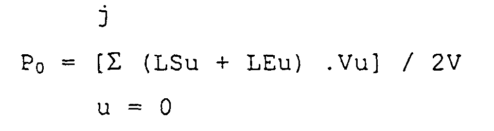 j représente le nombre de groupes d'intervalles secondaires,u représente une étiquette numérique de chaque groupe d'intervalles secondaires,LSu représente la position de début de chaque groupe d'intervalles secondaires u,LEu représente la position de fin de chaque groupe d'intervalles secondaires u,Vu représente le nombre d'apparitions des crêtes dans chaque groupe d'intervalles secondaires u, etV représente le nombre total d'apparitions des crêtes dans l'ensemble des groupes d'intervalles secondaires.
 - Procédé de réception selon la revendication 27, dans lequel le calcul de la position de crête moyenne pondérée P0 comprend l'exécution des étapes d'un algorithme équivalent à l'équation suivante,dans laquelle
 r représente le nombre de groupes d'intervalles secondaires dont chacun contient un nombre supérieur ou égal à m crêtes,j représente le nombre de qroupes d'intervalles secondaires,u représente une étiquette numérique de chaque groupe d'intervalles secondaires,LSu représente la position de début de chaque groupe d'intervalles secondaires u,LEu représente la position de fin de chaque groupe d'intervalles secondaires u,v représente une étiquette numérique de chaque groupe d'intervalles secondaires ne contenant pas m crêtes,Vu représente le nombre d'apparitions des crêtes dans chaque groupe d'intervalles secondaires u,V représente le nombre total d'apparitions des crêtes dans l'ensemble des groupes d'intervalles secondaires, etXu représente la somme de toutes les amplitudes de crêtes dans chaque groupe d'intervalles secondaires u.
 - Procédé de réception selon la revendication 27, dans lequel le calcul de la position de crête moyenne pondérée P0 comprend l'exécution des étapes d'un algorithme équivalent à l'équation suivante,dans laquelle
 r représente le nombre de groupes d'intervalles secondaires dont chacun contient un nombre supérieur ou égal à m crêtes,j représente le nombre de groupes d'intervalles secondaires,u représente une étiquette numérique de chaque groupe d'intervalles secondaires,LSu représente la position de début de chaque groupe d'intervalles secondaires u,LEu représente la position de fin de chaque groupe d'intervalles secondaires u,v représente une étiquette numérique de chaque groupe d'intervalles secondaires ne contenant pas m crêtes,Vu représente le nombre d'apparitions des crêtes dans chaque groupe d'intervalles secondaires u,V représente le nombre total d'apparitions des crêtes dans l'ensemble des groupes d'intervalles secondaires, etXu représente la somme de toutes les amplitudes de crêtes dans chaque groupe d'intervalles secondaires u.
Applications Claiming Priority (12)
| Application Number | Priority Date | Filing Date | Title |
|---|---|---|---|
| JP33107089 | 1989-12-22 | ||
| JP331070/89 | 1989-12-22 | ||
| JP33107089A JP2711921B2 (ja) | 1989-12-22 | 1989-12-22 | キャリア検出方法および装置 |
| JP1522/90 | 1990-01-10 | ||
| JP152290 | 1990-01-10 | ||
| JP152290A JP2756010B2 (ja) | 1990-01-10 | 1990-01-10 | 同期確立方法および装置 |
| JP3364290A JP2729693B2 (ja) | 1990-02-16 | 1990-02-16 | Csk通信方式における受信方法および装置 |
| JP3364390 | 1990-02-16 | ||
| JP3364290 | 1990-02-16 | ||
| JP33643/90 | 1990-02-16 | ||
| JP33642/90 | 1990-02-16 | ||
| JP2033643A JPH03238942A (ja) | 1990-02-16 | 1990-02-16 | Csk通信方法および装置,csk送信方法および装置ならびにcsk受信方法および装置 |
Publications (3)
| Publication Number | Publication Date |
|---|---|
| EP0439807A2 EP0439807A2 (fr) | 1991-08-07 |
| EP0439807A3 EP0439807A3 (en) | 1992-12-30 |
| EP0439807B1 true EP0439807B1 (fr) | 2000-05-24 |
Family
ID=27453425
Family Applications (1)
| Application Number | Title | Priority Date | Filing Date |
|---|---|---|---|
| EP90125190A Expired - Lifetime EP0439807B1 (fr) | 1989-12-22 | 1990-12-21 | Système de communication à modulation par décalage de code |
Country Status (5)
| Country | Link |
|---|---|
| US (1) | US5132986A (fr) |
| EP (1) | EP0439807B1 (fr) |
| AU (2) | AU637175B2 (fr) |
| CA (1) | CA2032909C (fr) |
| DE (1) | DE69033552T2 (fr) |
Families Citing this family (59)
| Publication number | Priority date | Publication date | Assignee | Title |
|---|---|---|---|---|
| US5499265A (en) * | 1989-08-07 | 1996-03-12 | Omnipoint Data Company, Incorporated | Spread spectrum correlator |
| US5090024A (en) * | 1989-08-23 | 1992-02-18 | Intellon Corporation | Spread spectrum communications system for networks |
| JPH0537491A (ja) * | 1991-07-31 | 1993-02-12 | Clarion Co Ltd | スペクトラム拡散通信装置 |
| WO1993012597A1 (fr) | 1991-12-16 | 1993-06-24 | Omnipoint Corporation | Systeme de publication de donnes a etalement de spectre |
| AU674695B2 (en) * | 1992-07-31 | 1997-01-09 | Atheros Communications, Inc. | Spread spectrum communication system particularly suited for RF network communication |
| US5289498A (en) * | 1992-09-09 | 1994-02-22 | Echelon Corporation | Adaptive data recovery for spread spectrum systems |
| US5315615A (en) * | 1992-12-31 | 1994-05-24 | Gte Government Systems Corporation | DSSS communications correlation |
| JPH06350562A (ja) * | 1993-06-08 | 1994-12-22 | Ricoh Co Ltd | スペクトル拡散通信方式 |
| KR960003847B1 (ko) * | 1993-09-18 | 1996-03-22 | 삼성전자주식회사 | 대역 확산 통신 방식 데이타 변복조장치 |
| FR2710481B1 (fr) * | 1993-09-22 | 1995-10-20 | Snecma | Procédé et dispositif de transmission de données par étalement de spectre à séquence directe. |
| US5666379A (en) * | 1993-11-01 | 1997-09-09 | Omnipoint Corporation | Best-of-M pulse position modulation detector |
| WO1995012945A1 (fr) * | 1993-11-01 | 1995-05-11 | Omnipoint Corporation | Desetalement/demodulation de signaux a spectre etale en sequence directe |
| US5515396A (en) * | 1994-02-25 | 1996-05-07 | Motorola, Inc. | Method and apparatus for selecting a spreading code in a spectrum spread communication system |
| JP3142222B2 (ja) * | 1994-08-22 | 2001-03-07 | 松下電器産業株式会社 | スペクトル拡散通信同期方法とその回路装置 |
| US5953370A (en) | 1994-09-09 | 1999-09-14 | Omnipoint Corporation | Apparatus for receiving and correlating a spread spectrum signal |
| US5648982A (en) * | 1994-09-09 | 1997-07-15 | Omnipoint Corporation | Spread spectrum transmitter |
| US5692007A (en) | 1994-09-09 | 1997-11-25 | Omnipoint Corporation | Method and apparatus for differential phase encoding and decoding in spread-spectrum communication systems with continuous-phase modulation |
| US5754585A (en) | 1994-09-09 | 1998-05-19 | Omnipoint Corporation | Method and apparatus for serial noncoherent correlation of a spread spectrum signal |
| US5881100A (en) | 1994-09-09 | 1999-03-09 | Omnipoint Corporation | Method and apparatus for coherent correlation of a spread spectrum signal |
| US5659574A (en) | 1994-09-09 | 1997-08-19 | Omnipoint Corporation | Multi-bit correlation of continuous phase modulated signals |
| US5754584A (en) | 1994-09-09 | 1998-05-19 | Omnipoint Corporation | Non-coherent spread-spectrum continuous-phase modulation communication system |
| US5680414A (en) | 1994-09-09 | 1997-10-21 | Omnipoint Corporation | Synchronization apparatus and method for spread spectrum receiver |
| US5832028A (en) * | 1994-09-09 | 1998-11-03 | Omnipoint Corporation | Method and apparatus for coherent serial correlation of a spread spectrum signal |
| US5629956A (en) * | 1994-09-09 | 1997-05-13 | Omnipoint Corporation | Method and apparatus for reception and noncoherent serial correlation of a continuous phase modulated signal |
| US5757847A (en) | 1994-09-09 | 1998-05-26 | Omnipoint Corporation | Method and apparatus for decoding a phase encoded signal |
| US5610940A (en) * | 1994-09-09 | 1997-03-11 | Omnipoint Corporation | Method and apparatus for noncoherent reception and correlation of a continous phase modulated signal |
| US5627856A (en) * | 1994-09-09 | 1997-05-06 | Omnipoint Corporation | Method and apparatus for receiving and despreading a continuous phase-modulated spread spectrum signal using self-synchronizing correlators |
| US5963586A (en) | 1994-09-09 | 1999-10-05 | Omnipoint Corporation | Method and apparatus for parallel noncoherent correlation of a spread spectrum signal |
| US5856998A (en) | 1994-09-09 | 1999-01-05 | Omnipoint Corporation | Method and apparatus for correlating a continuous phase modulated spread spectrum signal |
| US5818821A (en) | 1994-12-30 | 1998-10-06 | Intelogis, Inc. | Universal lan power line carrier repeater system and method |
| US5745484A (en) * | 1995-06-05 | 1998-04-28 | Omnipoint Corporation | Efficient communication system using time division multiplexing and timing adjustment control |
| US6356607B1 (en) | 1995-06-05 | 2002-03-12 | Omnipoint Corporation | Preamble code structure and detection method and apparatus |
| US5629639A (en) * | 1995-06-07 | 1997-05-13 | Omnipoint Corporation | Correlation peak detector |
| US5687190A (en) * | 1995-10-20 | 1997-11-11 | Otc Telecom | Non-coherent direct sequence spread spectrum receiver for detecting bit/symbol chip sequences using threshold comparisons of chip sequence correlations |
| US6678311B2 (en) | 1996-05-28 | 2004-01-13 | Qualcomm Incorporated | High data CDMA wireless communication system using variable sized channel codes |
| US6141373A (en) * | 1996-11-15 | 2000-10-31 | Omnipoint Corporation | Preamble code structure and detection method and apparatus |
| US6282228B1 (en) * | 1997-03-20 | 2001-08-28 | Xircom, Inc. | Spread spectrum codes for use in communication |
| US6101213A (en) * | 1997-03-21 | 2000-08-08 | Glynn Scientific, Inc. | Method system and computer program product for spread spectrum communication using circular waveform shift-keying |
| US5946344A (en) * | 1997-04-07 | 1999-08-31 | Intermec Ip Corp. | Multiple-rate direct sequence architecture utilizing a fixed chipping rate and variable spreading code lengths |
| JP3380446B2 (ja) * | 1997-10-20 | 2003-02-24 | 株式会社鷹山 | Cdma通信システム用受信装置 |
| US6560338B1 (en) * | 1998-08-28 | 2003-05-06 | Qualcomm Incorporated | Limiting delays associated with the generation of encryption stream ciphers |
| IL127223A (en) * | 1998-11-24 | 2002-08-14 | Systel Dev And Ind Ltd | Power-line digital communication system |
| US6868419B1 (en) * | 1999-10-28 | 2005-03-15 | Lightwaves Systems Inc. | Method of transmitting data including a structured linear database |
| US8085813B2 (en) * | 1999-10-28 | 2011-12-27 | Lightwaves Systems, Inc. | Method for routing data packets using an IP address based on geo position |
| US9900734B2 (en) | 1999-10-28 | 2018-02-20 | Lightwaves Systems, Inc. | Method for routing data packets using an IP address based on geo position |
| JP4072299B2 (ja) * | 1999-11-30 | 2008-04-09 | シャープ株式会社 | マッチドフィルタおよびそれを用いた大規模集積回路と通信システム |
| US7983349B2 (en) * | 2001-03-20 | 2011-07-19 | Lightwaves Systems, Inc. | High bandwidth data transport system |
| US8766773B2 (en) | 2001-03-20 | 2014-07-01 | Lightwaves Systems, Inc. | Ultra wideband radio frequency identification system, method, and apparatus |
| US7545868B2 (en) * | 2001-03-20 | 2009-06-09 | Lightwaves Systems, Inc. | High bandwidth data transport system |
| US6727790B2 (en) * | 2001-08-20 | 2004-04-27 | Itran Communications Ltd. | Acquisition of sychronization in a spread spectrum communications transceiver |
| US7577188B1 (en) * | 2001-09-13 | 2009-08-18 | Cisco Technology, Inc. | Physical layer and MAC enhancements using complex sequences on a wireless channel |
| US7961705B2 (en) * | 2003-04-30 | 2011-06-14 | Lightwaves Systems, Inc. | High bandwidth data transport system |
| US7876738B2 (en) * | 2004-03-02 | 2011-01-25 | Nokia Corporation | Preventing an incorrect synchronization between a received code-modulated signal and a replica code |
| CN101204020A (zh) * | 2005-06-23 | 2008-06-18 | 皇家飞利浦电子股份有限公司 | 使用低复杂度发射机增加对噪声免疫力的感应通信系统 |
| US8345778B2 (en) * | 2007-10-29 | 2013-01-01 | Lightwaves Systems, Inc. | High bandwidth data transport system |
| US8718115B2 (en) * | 2010-10-08 | 2014-05-06 | Texas Instruments Incorporated | Building, transmitting, and receiving frame structures in power line communications |
| US10602548B2 (en) * | 2017-06-22 | 2020-03-24 | Infineon Technologies Ag | System and method for gesture sensing |
| US10742258B1 (en) * | 2018-09-26 | 2020-08-11 | Novatel Inc. | System and method for demodulating code shift keying data utilizing correlations with combinational PRN codes generated for different bit positions |
| US10742257B1 (en) * | 2018-09-26 | 2020-08-11 | Novatel Inc. | System and method for demodulating code shift keying data from a satellite signal utilizing a binary search |
Family Cites Families (4)
| Publication number | Priority date | Publication date | Assignee | Title |
|---|---|---|---|---|
| US3244986A (en) * | 1962-10-08 | 1966-04-05 | Ibm | Detection of bi-phase digital signals |
| US3665474A (en) * | 1966-08-19 | 1972-05-23 | Amscat Corp | High density communications system |
| US4707839A (en) * | 1983-09-26 | 1987-11-17 | Harris Corporation | Spread spectrum correlator for recovering CCSK data from a PN spread MSK waveform |
| AU617885B2 (en) * | 1988-10-24 | 1991-12-05 | Nec Corporation | Spectrum spread communication by csk modulation |
-
1990
- 1990-12-21 US US07/631,921 patent/US5132986A/en not_active Expired - Lifetime
- 1990-12-21 AU AU68384/90A patent/AU637175B2/en not_active Ceased
- 1990-12-21 CA CA002032909A patent/CA2032909C/fr not_active Expired - Fee Related
- 1990-12-21 EP EP90125190A patent/EP0439807B1/fr not_active Expired - Lifetime
- 1990-12-21 DE DE69033552T patent/DE69033552T2/de not_active Expired - Fee Related
-
1993
- 1993-02-24 AU AU33792/93A patent/AU643400B2/en not_active Ceased
Also Published As
| Publication number | Publication date |
|---|---|
| AU6838490A (en) | 1991-06-27 |
| AU3379293A (en) | 1993-04-22 |
| AU643400B2 (en) | 1993-11-11 |
| CA2032909A1 (fr) | 1991-06-23 |
| US5132986A (en) | 1992-07-21 |
| DE69033552D1 (de) | 2000-06-29 |
| CA2032909C (fr) | 1995-10-10 |
| DE69033552T2 (de) | 2001-02-08 |
| EP0439807A3 (en) | 1992-12-30 |
| AU637175B2 (en) | 1993-05-20 |
| EP0439807A2 (fr) | 1991-08-07 |
Similar Documents
| Publication | Publication Date | Title |
|---|---|---|
| EP0439807B1 (fr) | Système de communication à modulation par décalage de code | |
| US5396515A (en) | Asymmetric spread spectrum correlator | |
| US6023489A (en) | Method and apparatus for code synchronization in a global positioning system receiver | |
| US5093841A (en) | Clock acquisition in a spread spectrum system | |
| US4964138A (en) | Differential correlator for spread spectrum communication system | |
| US5719900A (en) | Dual-threshold spread spectrum correlator | |
| WO1992020178A1 (fr) | Correlateur de spectre disperse | |
| WO1992002094A1 (fr) | Procede et appareil de detection de phase utilisant un correlateur d'ondes acoustiques de surface | |
| US6657986B1 (en) | Variable clock rate correlation circuit and method of operation | |
| US5495509A (en) | High processing gain acquisition and demodulation apparatus | |
| CA2001349C (fr) | Methode de communication a spectre etale utilisant la modulation csk | |
| US6335946B1 (en) | Method and a device for broadband transmission | |
| EP0358581B1 (fr) | Système de détection d'un mot unique | |
| AU702961B2 (en) | CSK communication system and method for spread spectrum communication | |
| JPH10285078A (ja) | スペクトル直接拡散通信システムにおける相関同期回路 | |
| US5285458A (en) | System for suppressing spread of error generated in differential coding | |
| JP2596988B2 (ja) | スペクトラム拡散通信方式および装置 | |
| US4012696A (en) | Multiple rate digital command detection system with range clean-up capability | |
| JP3391820B2 (ja) | スペクトル拡散通信装置 | |
| RU2127486C1 (ru) | Способ и устройство передачи сообщений широкополосными сигналами | |
| WO1992016064A1 (fr) | Correlateur asymetrique de spectre etale | |
| JPH10107684A (ja) | スペクトル拡散通信方法及び装置 | |
| JP3322915B2 (ja) | スペクトル拡散通信における同期追跡方法および同期追跡装置 | |
| KR100224578B1 (ko) | 디지탈 위상폐루프회로를 이용한 타이밍복원방법 및 그 장치 | |
| SU1354431A1 (ru) | Система передачи информации |
Legal Events
| Date | Code | Title | Description |
|---|---|---|---|
| PUAI | Public reference made under article 153(3) epc to a published international application that has entered the european phase |
Free format text: ORIGINAL CODE: 0009012 |
|
| AK | Designated contracting states |
Kind code of ref document: A2 Designated state(s): DE FR GB NL |
|
| PUAL | Search report despatched |
Free format text: ORIGINAL CODE: 0009013 |
|
| AK | Designated contracting states |
Kind code of ref document: A3 Designated state(s): DE FR GB NL |
|
| 17P | Request for examination filed |
Effective date: 19930405 |
|
| 17Q | First examination report despatched |
Effective date: 19940502 |
|
| GRAG | Despatch of communication of intention to grant |
Free format text: ORIGINAL CODE: EPIDOS AGRA |
|
| GRAG | Despatch of communication of intention to grant |
Free format text: ORIGINAL CODE: EPIDOS AGRA |
|
| GRAH | Despatch of communication of intention to grant a patent |
Free format text: ORIGINAL CODE: EPIDOS IGRA |
|
| GRAH | Despatch of communication of intention to grant a patent |
Free format text: ORIGINAL CODE: EPIDOS IGRA |
|
| GRAA | (expected) grant |
Free format text: ORIGINAL CODE: 0009210 |
|
| AK | Designated contracting states |
Kind code of ref document: B1 Designated state(s): DE FR GB NL |
|
| REF | Corresponds to: |
Ref document number: 69033552 Country of ref document: DE Date of ref document: 20000629 |
|
| ET | Fr: translation filed | ||
| PGFP | Annual fee paid to national office [announced via postgrant information from national office to epo] |
Ref country code: NL Payment date: 20001231 Year of fee payment: 11 |
|
| REG | Reference to a national code |
Ref country code: GB Ref legal event code: 732E |
|
| RAP2 | Party data changed (patent owner data changed or rights of a patent transferred) |
Owner name: NEC CORPORATION |
|
| PLBE | No opposition filed within time limit |
Free format text: ORIGINAL CODE: 0009261 |
|
| STAA | Information on the status of an ep patent application or granted ep patent |
Free format text: STATUS: NO OPPOSITION FILED WITHIN TIME LIMIT |
|
| NLS | Nl: assignments of ep-patents |
Owner name: NEC CORPORATION |
|
| NLT2 | Nl: modifications (of names), taken from the european patent patent bulletin |
Owner name: NEC CORPORATION |
|
| REG | Reference to a national code |
Ref country code: FR Ref legal event code: TP |
|
| 26N | No opposition filed | ||
| REG | Reference to a national code |
Ref country code: GB Ref legal event code: IF02 |
|
| PG25 | Lapsed in a contracting state [announced via postgrant information from national office to epo] |
Ref country code: NL Free format text: LAPSE BECAUSE OF NON-PAYMENT OF DUE FEES Effective date: 20020701 |
|
| NLV4 | Nl: lapsed or anulled due to non-payment of the annual fee |
Effective date: 20020701 |
|
| PGFP | Annual fee paid to national office [announced via postgrant information from national office to epo] |
Ref country code: FR Payment date: 20031210 Year of fee payment: 14 |
|
| PGFP | Annual fee paid to national office [announced via postgrant information from national office to epo] |
Ref country code: GB Payment date: 20031217 Year of fee payment: 14 |
|
| PGFP | Annual fee paid to national office [announced via postgrant information from national office to epo] |
Ref country code: DE Payment date: 20040102 Year of fee payment: 14 |
|
| PG25 | Lapsed in a contracting state [announced via postgrant information from national office to epo] |
Ref country code: GB Free format text: LAPSE BECAUSE OF NON-PAYMENT OF DUE FEES Effective date: 20041221 |
|
| PG25 | Lapsed in a contracting state [announced via postgrant information from national office to epo] |
Ref country code: DE Free format text: LAPSE BECAUSE OF NON-PAYMENT OF DUE FEES Effective date: 20050701 |
|
| GBPC | Gb: european patent ceased through non-payment of renewal fee |
Effective date: 20041221 |
|
| PG25 | Lapsed in a contracting state [announced via postgrant information from national office to epo] |
Ref country code: FR Free format text: LAPSE BECAUSE OF NON-PAYMENT OF DUE FEES Effective date: 20050831 |
|
| REG | Reference to a national code |
Ref country code: FR Ref legal event code: ST |