EP0439011B1 - Distance measurement device - Google Patents
Distance measurement device Download PDFInfo
- Publication number
- EP0439011B1 EP0439011B1 EP91100115A EP91100115A EP0439011B1 EP 0439011 B1 EP0439011 B1 EP 0439011B1 EP 91100115 A EP91100115 A EP 91100115A EP 91100115 A EP91100115 A EP 91100115A EP 0439011 B1 EP0439011 B1 EP 0439011B1
- Authority
- EP
- European Patent Office
- Prior art keywords
- light
- distance measuring
- measuring apparatus
- accordance
- switching
- Prior art date
- Legal status (The legal status is an assumption and is not a legal conclusion. Google has not performed a legal analysis and makes no representation as to the accuracy of the status listed.)
- Expired - Lifetime
Links
Images


Classifications
-
- G—PHYSICS
- G01—MEASURING; TESTING
- G01S—RADIO DIRECTION-FINDING; RADIO NAVIGATION; DETERMINING DISTANCE OR VELOCITY BY USE OF RADIO WAVES; LOCATING OR PRESENCE-DETECTING BY USE OF THE REFLECTION OR RERADIATION OF RADIO WAVES; ANALOGOUS ARRANGEMENTS USING OTHER WAVES
- G01S7/00—Details of systems according to groups G01S13/00, G01S15/00, G01S17/00
- G01S7/48—Details of systems according to groups G01S13/00, G01S15/00, G01S17/00 of systems according to group G01S17/00
- G01S7/483—Details of pulse systems
- G01S7/484—Transmitters
-
- G—PHYSICS
- G01—MEASURING; TESTING
- G01S—RADIO DIRECTION-FINDING; RADIO NAVIGATION; DETERMINING DISTANCE OR VELOCITY BY USE OF RADIO WAVES; LOCATING OR PRESENCE-DETECTING BY USE OF THE REFLECTION OR RERADIATION OF RADIO WAVES; ANALOGOUS ARRANGEMENTS USING OTHER WAVES
- G01S7/00—Details of systems according to groups G01S13/00, G01S15/00, G01S17/00
- G01S7/48—Details of systems according to groups G01S13/00, G01S15/00, G01S17/00 of systems according to group G01S17/00
- G01S7/497—Means for monitoring or calibrating
Definitions
- the invention relates to a distance measuring device according to the preamble of patent claim 1.
- Such distance measuring devices are used, for example, to measure distances in the range from 2 to 10 m from the distance measuring device electronically, the measuring accuracy being in the range of a few mm. In this way, the fill levels of containers or, for example, the fill levels of shelves can be measured and reported electronically to a control center.
- Such distance measuring devices normally use a measuring and a reference receiver, which entails the risk of different drifting of the two receiving circuits and also leads to disadvantageous influences of different junction capacitance or response time changes of the two photodiodes used for the reception.
- the use of only one light-emitting diode has the problem that crosstalk between the measuring and reference sections cannot be ruled out.
- a distance measuring method is known from EP 0 066 888 A, in which the transit time of a measuring light pulse is evaluated, which emits from a transmitter on the basis of a trigger signal, is reflected from the target object to the measured value, and is converted there into an electrical signal by a receiver, which to generate a stop signal for a Signal runtime measurement is used, which has been started depending on the time of emission of the measuring light pulse.
- at least one signal transit time measurement is carried out over the measuring section and, separately therefrom, at least one signal transit time measurement is carried out via a device-internal reference link and the distance measured value is determined from the difference between the at least two signal transit time values.
- a method for distance measurement is known from EP 0 091 665 A, in which modulated light is emitted by a light source, reflected by a point whose distance from the light source is to be determined, and received by a receiver element.
- the distance to be determined is calculated from the phase difference between the emitted and the received light signal.
- the light receiver therefore has only a single optoelectronic light-receiving element which alternates the light wave trains from the measuring section and from the reference route receives. This reception takes place sequentially.
- phase comparison of these light wave trains emitted one after the other is solved according to the invention in that the received signals are fed to a multiplicative mixing stage which also receives an adjustable wave train signal which is identical in frequency and known in phase (90 ° grid). In this way, an absolute measurement of the phase of both the wave train signal passed over the measurement section and the wave train signal reaching the receiver via the reference section can be carried out.
- signals representative of the absolute phase of both the measuring section wave train and the reference section wave train appear in succession, which can then be correlated without problems in the microcomputer.
- reception circuit Since there is only a single reception channel and all phase signals that are subsequently subtracted from one another in the microcomputer, with the exception of the two complementarily switched light sources, pass through all the lines and components equally, the reception circuit is insensitive to drift.
- the signal / noise ratio of the received signals is improved, because this improves the useful signal from the noise background.
- the crosstalk attenuation of the measurement and reference channel is extremely high due to the complementary switching light sources.
- the measuring and reference path can be chosen largely independently of the place of its beginning, since an arbitrarily chosen starting point can easily be taken into account in the subsequent evaluation due to the absolute phase measurement by means of the mixing stage.
- Claims 6 to 8 describe advantageous exemplary embodiments for the switching and control of the laser diodes.
- a particularly expedient intensity control for the laser diodes results from claim 12.
- the invention therefore relates to a device for the self-calibration of distance measuring devices according to the transit time method.
- a runtime-neutral electronic switchover between a measuring path and a reference path is provided by two optoelectronic transmitters, preferably semiconductor laser diodes.
- Semiconductor switches in particular switch diodes, can be used for the switching device. If the respective laser is separated from the working circuit, a switch diode simultaneously ensures decoupling from the modulation circuit with the corresponding high-frequency information.
- the laser is supplied with an auxiliary voltage in the reverse direction.
- the active switching process is triggered by two auxiliary switches, preferably transistor switches, in the low-frequency part of the control loop. These can be used simultaneously as actuators of a PI controller common to both lasers will.
- the control loop is closed by a current sum circuit of both monitor diodes.
- the disadvantages that would arise if a reference were taken by a reference receiver are thus avoided.
- the high modulation bandwidth of the laser diodes in conjunction with diode switches enables good runtime consistency and thus a low offset drift for self-calibration.
- the reception path can be made narrow-band (selective) and thus less sensitive to external interference or noise. This can improve the detectability.
- a mother oscillator 43 generates a frequency of 10 MHz, for example, which is fed via a phase comparator 44 to a variable oscillator 45 which is connected to a digital phase shifter 46.
- One output P 'of the digital phase shifter 46 is fed back to the second input of the phase comparator 44, whereby a phase lock loop is formed, on the basis of which the variable oscillator outputs a frequency of 300 MHz to the digital phase shifter 46.
- the frequency setting can be brought about by that a suitable frequency setting signal is fed to the phase comparator 44 at 87 by a microprocessor 16.
- the output signal P 'of the digital phase shifter 46 is also fed to the one input of a mixer 47 which mixes this signal additively or multiplicatively with a signal coming from a light receiver 12.
- An approximation filter 48 which is particularly narrow-band, is connected to the output of the mixer stage 47.
- the phase adjustment of the digital phase shifter 46 takes place at 88 from the microprocessor 16.
- phase pairs with a frequency of 75 MHz which can be set in 90 ° increments, are generated one after the other and forwarded to the transmitter 11 or the mixer 47 as corresponding wave train signals P or P '.
- two laser diodes 18, 19 connected complementarily by the microprocessor 16 via the connection 89 are provided, one of which (18) emits a high-frequency modulated light wave train to a target 13 via a measuring section 14, from which the light is reflected back to the receiver 12 arranged directly next to the light transmitter 11, in which only a single photodiode 20 is arranged, which contains both the light from the measuring section 14 and from a reference path 15 accommodated in the same housing 17 as light transmitter 11 and light receiver 12, which is received by the second laser diode 19 is loaded.
- the reception circuit tuning in the receiver 12 is carried out by the microprocessor 16 at 91.
- a control line 92 also leads from the light receiver 12 to the microprocessor 16, on the basis of which the dynamic evaluation is carried out by the latter.
- the approximation filter 48 is also acted upon by the microprocessor 16 via a control line 93 and its bandwidth is controlled.
- the output of the approximation filter 48 is applied via an analog-digital circuit 49 to the microprocessor 16, which carries out the signal evaluation in the following way:
- Each of the wave trains emitted by the digital phase shifter 46 and each phase-shifted by 90 ° to one another is directly (P ') on one input of the mixer 47 and on the other at P via the transmitter 11 and alternately the measuring section 14 or the reference section 15 and the Given light receiver 12 to the other input of the measuring stage 47, where a multiplication with the signal P 'takes place. Because of the phase shift between the light wave trains passing through the measuring section 14 and the reference section 15, different phase signals will appear at the output of the approximation filter, from which the different transit times of the light wave trains over the measuring section 14 on the one hand and the reference section 15 on the other hand can be concluded, which in the Microprocessor 16 is evaluated. Taking into account the speed of light, the distance of the housing 17 from the target 13 can be determined.
- the light transmitter 11 has two laser diodes 18, 19, one of which supplies the measuring section 14 and the other the reference section 15 with a bundled light beam.
- the laser diodes 18, 19 with their positive poles are each connected via an auxiliary switch 21, 22 with an associated controller at 23 to a positive supply voltage source with a voltage of, for example, +5.2 V.
- the negative poles of the laser diodes 18, 19 are applied via a high-frequency switch 24 or 25 to a grounded inductor 33, which forms part of a high-pass filter, which also includes a capacitor 34, which is acted upon by schematically indicated high-frequency modulation voltage terminals 26, 27, which the wave train signals P (Fig.1) are fed.
- a negative auxiliary voltage of e.g. -12 V connected.
- the auxiliary switches with control 21, 22 are connected to terminals 18th ⁇ respectively. 19th ⁇ Switching signals applied complementary to each other. If - as shown in Fig. 2 - the switch 21 is closed, the other switch 22 is open and vice versa.
- Each laser diode 18, 19 is assigned a monitor diode 18 'or 19', which alternately actuate a PI controller 41, which also from the switch terminals 18th ⁇ respectively. 19th ⁇ according to the position of the auxiliary switches 21, 22, alternately connected setpoints S1 and S2 are supplied.
- the PI controller 41 emits control control signals for the control part of the switches 21, 22 at 94, 95.
- the current to the laser diodes 18, 19 can be adjusted so that the light intensity of the laser diodes 18, 19 is constant.
- the setpoint supply S1, S2 it can further be ensured that a degradation of the laser diodes 18, 19 is counteracted by a greater opening of the regulators of the switches 21, 22.
- Certain light intensities can also be preset by changing the setpoints S1 and S2.
- Capacitors 35, 37 between the positive poles of the laser diodes 18, 19 and ground represent a high-pass filter for the high-frequency modulation voltage supplied via the diode switches 24, 25.
- the circuit according to FIG. 2 works as follows:
- Switching signals for the switches 21, 22 are supplied via the switching terminals 18, 19 in such a way that one switch is always closed and the other is open.
- the high-frequency switches 24, 25 are also closed or opened synchronously therewith, which is indicated by dashed coupling lines 96, 97. If the switches 21, 24 (see left-hand illustration in FIG. 2) are closed, the associated laser diode 18 lies between the positive supply voltage terminal 23 and ground and is therefore switched on. Via the high-pass filter 33, 34, 35, the direct current flowing through the laser diode 18 is simultaneously modulated with a corresponding high-frequency voltage of, for example, 75 MHz.
- the switching signal switches at the switching terminal 18th ⁇ the switch 21 and thus also the switch 24 back to the open position, while a complementary switching signal at the switching terminal 19th ⁇ closes the switch with controller 22 and the high-frequency switch 25.
- the work cycle on the laser diode 19 now continues accordingly, and the light wave trains are sent over the reference path 15 (FIG. 1).
- the assigned monitor diode 18 'or 19' emits an actual value signal to the PI controller 41 via a common line 98.
- the switching signals on the switching terminals ensure 18th ⁇ , 19th ⁇ to ensure that the setpoint signal S1 or S2 assigned to the relevant laser diode 18 or 19 is also fed to the PI controller, which then adjusts the controller of the relevant switch 21 or 22 accordingly such that the laser diodes 18, 19 emit light wave trains with a predetermined intensity.
- the two laser diodes 18, 19 are applied, on the one hand, to the positive supply voltage terminal 23, which is at a potential of +5.2 V, via a switching regulating transistor 21 or 22 and a resistor 50, 51 connected in its emitter circuit.
- the negative pole of the laser diodes 18, 19, on the other hand, is connected to ground via a respective switching diode 24 or 25, which forms a high-frequency switch in the same direction as the laser diodes 18, 19, and a common inductor 32, the potential of which is supplied via a terminal 52.
- the inductor 33 is part of a high-pass filter which also has a capacitor 34 and which is connected via a resistor 53 to a modulation driver stage 54 which consists of two transistors connected to one another by means of the bases and the associated resistors and is likewise connected between ground and the DC supply voltage terminal 23.
- a capacitor 55 and an inductor 56 keep the high-frequency modulation voltage away from the DC supply line.
- the output voltage of a transformer 59 is connected to the emitter of one transistor of the driver stage 54 via a resistor 57 and a capacitor 58, the input winding of which is connected via a potentiometer 60 to the high-frequency modulation voltage terminals 26, 27, which receives the wave train signals P (FIG. 1 ) are fed.
- the positive lead to the laser diodes 18, 19 is connected to ground via high-frequency discharge capacitors 35, 36 and 37, 38 and to a terminal 28 for supplying an auxiliary voltage of -12 V via high-resistance resistors 29 and 30.
- connection point between the laser diodes 18, 19 and the associated switching diodes 24, 25 is also connected to the positive lead of the laser diodes 18, 19 via an auxiliary diode 61 and 62 connected against the laser diodes 18, 19.
- the pole of the auxiliary diodes 61, 62 facing away from the transistors 21, 22 is also grounded via a resistor 63, 64.
- Each laser diode 18, 19 is assigned a monitor diode 18 ', 19' which, on the one hand, is applied to the positive lead and, on the other hand, is connected to the input of the PI controller 41 via diodes 39, 40 which are switched on in the same direction as the diodes 24, 25 , which contains two operational amplifiers 65 and 66 connected in series.
- the operating voltages are derived in the manner shown from the terminal 28 lying at -12 V and a further terminal 67 lying at +12 V.
- the minus input terminal of the operational amplifier 66 is alternately supplied with two set signals S1, S2, which are derived from a terminal 42 carrying an exact constant DC voltage via set value adjustment potentiometers 68 and 69 and switching transistors 70 and 71 connected in parallel.
- the DC voltage is supplied to the potentiometers 68, 69 via switching transistors 70, 71, which are used by the 18th ⁇ , 19th ⁇ applied switching signals are opened and closed synchronously with the laser diodes 18, 19. In this way, when each laser diode 18 or 19 is switched on, the setpoint S1 or S2 provided for the laser diode in question is supplied to the input of the operational amplifier 66.
- the output of the PI controller 41 is fed via resistors 72 and 73 to the collector of a switching transistor 31 and 32, which is applied to the positive DC supply voltage +5.2 V in the manner shown via a diode 74 or 75.
- the positive DC supply line is grounded via a capacitor 76 for further high-frequency decoupling.
- the collector of the switching transistors 31 and 32 is connected to the terminals via a resistor 77 and 78, respectively 18th ⁇ respectively. 19th ⁇ the switching voltage for the laser diodes 18, 19 supplied.
- the emitters of the switching transistors 31, 32 are applied to the positive DC voltage terminal 23 via capacitors 79 and 80 and resistors 81 and 82, respectively. It is also connected to the base of the transistor 21 or 22, the emitter of which, as already mentioned above, is connected to the positive supply voltage +5.2 V via a resistor 50 or 51 and the collector of which is connected to the positive supply line for the laser diodes 18 or 19 is connected.
- a voltage is tapped from the emitters of the control switching transistors 21 and 22 via resistors 83 and 84, respectively, and led to a terminal 85.
- This signal is representative of the current flowing through the laser diodes 18, 19 and can be used in the microprocessor 16 (FIG. 1) to monitor the control circuit for compliance with the laser protection class or the degradation of both lasers.
- a further monitoring terminal 86 is also provided, which is connected via a resistor 87 to the output of the operational amplifier 65 of the PI controller 41. Since this signal is dependent on the light exposure of the monitor diodes 18 ', 19', it is representative of the brightness of the laser diodes 18, 19 at a certain applied current, which in turn can be measured at the terminal 85. In this way, the microprocessor 16, to which the terminals 85, 86 are connected, can determine if, for example, the light output for a specific diode current is decreasing, which can then be taken into account in the evaluation.
- the microprocessor 16 alternately emits switch-on signals for the laser diodes 18 and 19, which open the control switching transistors 21, 22 via the switching transistors 31 and 32, respectively, in such a way that only one of the transistors 21 or 22 opens at a time , the other is closed.
- the direct current required for lighting up is supplied via the resistor 50 of the laser diode 18 or via the resistor 51 of the laser diode 19, which flows through the switching diodes 24 or 25 and the inductor 33 to ground.
- a laser diode e.g. 18 can be activated via the now open switching diode, e.g. 24, from high-pass 33, 34, the high-frequency modulation voltage applied at 26, 27 to the associated laser diode, e.g. 18, arrive. It is dissipated to ground via the capacitors 35, 36 or 37, 38. In this way, the modulation of the laser diodes 18, 19 takes place while they are being acted upon by a direct voltage that lights them up. The depth of the modulation is so great that the diodes go out and light up again during the modulation in rhythm with the supplied high-frequency modulation voltage and can be adjusted using the potentiometer 60.
- the degree of opening of the control switching transistors 21 and 22 is adjusted so that the laser diodes 18 and 19 adjust the light intensity set on the potentiometers 68 and 69, respectively accept.
- the control switching transistors 21, 22 thus fulfill a double function as actuators of the control circuit and also as a switch for switching the laser diodes 18, 19 on and off.
- the switching diodes 24, 25 carry both the direct laser current and the superimposed modulation high-frequency current. They are high-frequency switches because they open when the assigned laser diode 18 or 19 is switched off and close again when the switch is switched on.
- the positive leads are connected to a negative auxiliary voltage via the resistors 29, 30, so that a voltage which completely blocks the laser diodes is applied to them in these periods.
- the laser diodes 18 or 19 are switched off, there is a voltage divider in each case via the resistor 63, the diode 61 and the resistor 29 or the resistor 64, the diode 62 and the resistor 30.
- the diodes 61, 62 limit this auxiliary voltage to a permissible value. As a result, the desired properties, in particular the lighting up of the laser diodes, are only supported in the desired periods.
- the brightness of the two laser diodes can be preset using potentiometers 68 or 69.
- the control bandwidth of the PI controller 41 is very much smaller than the modulation frequency.
Landscapes
- Engineering & Computer Science (AREA)
- Computer Networks & Wireless Communication (AREA)
- Physics & Mathematics (AREA)
- General Physics & Mathematics (AREA)
- Radar, Positioning & Navigation (AREA)
- Remote Sensing (AREA)
- Optical Radar Systems And Details Thereof (AREA)
- Measurement Of Optical Distance (AREA)
- Length Measuring Devices By Optical Means (AREA)
Description
Die Erfindung betrifft ein Abstandsmeßgerät nach dem Oberbegriff des Patentanspruchs 1.The invention relates to a distance measuring device according to the preamble of patent claim 1.
Derartige Abstandsmeßgeräte (DE-OS 34 29 062) dienen dazu, beispielsweise im Bereich von 2 bis 10 m liegende Abstände von dem Abstandsmeßgerät auf elektronischem Wege zu messen, wobei die Meßgenauigkeit im Bereich einiger mm liegt. Auf diese Weise können die Füllstände von Behältern oder beispielsweise auch die Füllungsgrade von Regalen meßtechnisch erfaßt und auf elektronischem Wege zu einer Zentrale gemeldet werden.Such distance measuring devices (DE-OS 34 29 062) are used, for example, to measure distances in the range from 2 to 10 m from the distance measuring device electronically, the measuring accuracy being in the range of a few mm. In this way, the fill levels of containers or, for example, the fill levels of shelves can be measured and reported electronically to a control center.
Normalerweise verwenden derartige Abstandsmeßgeräte einen Meß- und einen Referenzempfänger, was die Gefahr eines unterschiedlichen Driftens der beiden Empfangsschaltungen mit sich bringt und außerdem zu nachteiligen Einflüssen unterschiedlicher Sperrschichtkapazitäten bzw. Reaktionszeitänderungen der beiden für den Empfang verwendeten Photodioden führt. Die Verwendung nur einer Lichtsendediode bringt andererseits das Problem mit sich, daß ein Übersprechen zwischen Meß- und Referenzstrecke nicht ausgeschlossen werden kann.Such distance measuring devices normally use a measuring and a reference receiver, which entails the risk of different drifting of the two receiving circuits and also leads to disadvantageous influences of different junction capacitance or response time changes of the two photodiodes used for the reception. On the other hand, the use of only one light-emitting diode has the problem that crosstalk between the measuring and reference sections cannot be ruled out.
Aus der EP 0 066 888 A ist ein Entfernungsmeßverfahren bekannt, bei dem die Laufzeit eines Meßlichtimpulses ausgewertet wird, der aufgrund eines Trigger-Signals von einem Sender emittiert, vom Zielgegenstand zum Meßwert reflektiert und dort durch einen Empfänger in ein elektrisches Signal umgesetzt wird, das zur Erzeugung eines Stop-Signals für eine Signal-Laufzeitmessung dient, die in Abhängigkeit vom Emissionszeitpunkt des Meßlichtimpulses gestartet worden ist. Dabei wird mindestens eine Signal-Laufzeitmessung über die Meßstrecke und getrennt hiervon mindestens eine Signal-Laufzeitmessung über eine geräteinterne Referenzstrecke durchgeführt und der Entfernungsmeßwert aus der Differenz der wenigstens zwei Signal-Laufzeitwerte ermittelt.A distance measuring method is known from EP 0 066 888 A, in which the transit time of a measuring light pulse is evaluated, which emits from a transmitter on the basis of a trigger signal, is reflected from the target object to the measured value, and is converted there into an electrical signal by a receiver, which to generate a stop signal for a Signal runtime measurement is used, which has been started depending on the time of emission of the measuring light pulse. In this case, at least one signal transit time measurement is carried out over the measuring section and, separately therefrom, at least one signal transit time measurement is carried out via a device-internal reference link and the distance measured value is determined from the difference between the at least two signal transit time values.
Aus der EP 0 091 665 A ist ein Verfahren zur Abstandsmessung bekannt, bei dem moduliertes Licht von einer Lichtquelle ausgesandt, von einem Punkt, dessen Abstand von der Lichtquelle zu ermitteln ist, reflektiert und von einem Empfängerelement empfangen wird. Der zu ermittelnde Abstand wird dabei aus der Phasendifferenz zwischen dem ausgesandten und dem empfangenen Lichtsignal berechnet.A method for distance measurement is known from EP 0 091 665 A, in which modulated light is emitted by a light source, reflected by a point whose distance from the light source is to be determined, and received by a receiver element. The distance to be determined is calculated from the phase difference between the emitted and the received light signal.
Die Aufgabe der Erfindung besteht darin, ein Abstandsmeßgerät zu schaffen, bei dem
- die Empfangsschaltung driftunempfindlich ist,
- das Signal/Rauschverhältnis verbessert wird und
- mit dem eine extrem hohe Übersprechdämpfung von Meß- und Referenzkanal möglich ist, wobei
- Meß- und Referenzstrecke weitgehend unabhängig vom Ort ihres Anfangs gewählt werden können.
- the receiving circuit is insensitive to drift,
- the signal / noise ratio is improved and
- with which an extremely high crosstalk attenuation of the measurement and reference channel is possible, whereby
- Measuring and reference distance can be chosen largely independently of the place of their beginning.
Zur Lösung sind die Merkmale des Anspruchs 1 vorgesehen.The features of claim 1 are provided for the solution.
Erfindungsgemäß weist also der Lichtempfänger nur ein einziges opto-elektronisches Licht-Empfangselement auf, welches abwechselnd die Lichtwellenzüge von der Meßstrecke und von der Referenzstrecke empfängt. Dieser Empfang erfolgt zeitlich nacheinander.According to the invention, the light receiver therefore has only a single optoelectronic light-receiving element which alternates the light wave trains from the measuring section and from the reference route receives. This reception takes place sequentially.
Die Problematik des Phasenvergleichs dieser zeitlich nacheinander ausgesandten Lichtwellenzüge wird erfindungsgemäß dadurch gelöst, daß die Empfangssignale einer multiplikativen Mischstufe zugeführt werden, die auch ein in der Frequenz identisches und in der Phase bekanntes (90°-Raster) einstellbares Wellenzugsignal empfängt. Auf diese Weise kann eine Absolutmessung der Phase sowohl des über die Meßstrecke gegangenen Wellenzug-Signals als auch des über die Referenzstrecke zum Empfänger gelangenden Wellenzugsignals durchgeführt werden.The problem of the phase comparison of these light wave trains emitted one after the other is solved according to the invention in that the received signals are fed to a multiplicative mixing stage which also receives an adjustable wave train signal which is identical in frequency and known in phase (90 ° grid). In this way, an absolute measurement of the phase of both the wave train signal passed over the measurement section and the wave train signal reaching the receiver via the reference section can be carried out.
Am Ausgang der Mischstufe bzw. des Approximationsfilters erscheinen somit zeitlich nacheinander für die Absolutphase sowohl des Meßstreckenwellenzugs als auch des Referenzstreckenwellenzugs repräsentative Signale, welche anschließend im Mikrocomputer problemlos korreliert werden können.At the output of the mixing stage or the approximation filter, signals representative of the absolute phase of both the measuring section wave train and the reference section wave train appear in succession, which can then be correlated without problems in the microcomputer.
Nachdem nur ein einziger Empfangskanal vorhanden ist und sämtliche später im Mikrocomputer voneinander subtrahierten Phasensignale mit Ausnahme der beiden komplementär geschalteten Lichtquellen sämtliche Leitungen und Bauelemente gleichermaßen durchlaufen, ist die Empfangsschaltung driftunempfindlich.Since there is only a single reception channel and all phase signals that are subsequently subtracted from one another in the microcomputer, with the exception of the two complementarily switched light sources, pass through all the lines and components equally, the reception circuit is insensitive to drift.
Aufgrund der im Approximationsfilter stattfindenden Integration ist das Signal/Rauschverhältnis der Empfangssignale verbessert, weil hierdurch das Nutzsignal aus dem Rauschuntergrund besser herausgehoben wird.Due to the integration taking place in the approximation filter, the signal / noise ratio of the received signals is improved, because this improves the useful signal from the noise background.
Die Übersprechdämpfung von Meß- und Referenzkanal ist wegen den komplementär schaltenden Lichtquellen extrem hoch.The crosstalk attenuation of the measurement and reference channel is extremely high due to the complementary switching light sources.
Meß- und Referenzstrecke können weitgehend unabhängig vom Ort ihres Anfangs gewählt werden, da ein willkürlich gewählter Anfangsort aufgrund der Phasenabsolutmessung mittels der Mischstufe ohne weiteres bei der späteren Auswertung berücksichtigt werden kann.The measuring and reference path can be chosen largely independently of the place of its beginning, since an arbitrarily chosen starting point can easily be taken into account in the subsequent evaluation due to the absolute phase measurement by means of the mixing stage.
Weiterhin können mit der Erfindung folgende Vorteile erzielt werden:
- Die Empfangsschaltung ist driftunempfindlich; Sperrschichtkapazitäts- bzw. Reaktionszeitänderungen der im Empfang verwendeten Photodiode werden vom Referenzpfad erfaßt.
- Es ist ein einfacher Betrieb mit Avalanche-Photodioden möglich; eine temperaturabhängige Spannungsnachführung verursacht Parameteränderungen der betreffenden Photodiode, welche jedoch von dem Referenzpfad erfaßt werden. Erfindungsgemäß ist nur eine Avalanche-Photodiode nötig.
- Das Signal-Rauschverhältnis wird verbessert; die Photodiodenkapazität kann erfindungsgemäß in einen Schwingkreis hoher Güte eingebunden werden, während der Realteil (Trans-impedanzwiderstand) bei gleichzeitiger hoher Arbeitsfrequenz vergrößert wird. Eine Phasendrift wird vom Referenzpfad erfaßt.
- Die Erzielung einer extrem hohen Übersprechdämpfung von Meß- und Referenzkanal ist möglich; der jeweils ausgeschaltete Laser kann insbesondere dann, wenn er gemäß Anspruch 4 mit einer negativen Spannung beaufschlagt ist, schaltungsbedingt kein optisches Signal aussenden. Die Übersprechdämpfung wird nur noch von der optischen Trennung zwischen Meß- und Referenzstrecke bzw. von elektromagnetischen Einkopplungen des Senders auf die Empfangseinrichtung bestimmt.
- Eine einfache Realisierung einer Kollimationsoptik für den Meßkanal ist auf diese Weise möglich; es wird keine Strahlaufspaltung für einen Referenzpfad benötigt. Die Referenzstrecke wird durch den Raum zwischen der Referenz-Laserdiode und der Empfangs-Photodiode bestimmt.
- Die Halbleiterumschaltung kann erfindungsgemäß vereinfacht werden; an die Halbleiterschalter werden in bezug auf die Sperrdämpfung keine hohen Anforderungen gestellt. Die Laufzeitdifferenzen des Schaltelementes können durch gute Anpassung der parasitären Größen wie Serienwiderstand und Sperrkapazität durch die Verwendung einer Doppeldiode sehr klein gehalten werden. Die Umschaltung kann mit hohen Pegeln erfolgen, was störtechnisch von Vorteil ist.
- Es wird eine geringe Laufzeitdrift erzielt; für Meß- und Referenzkanal können bis zur Diodenumschaltung gemeinsame Modulationspfade benutzt werden. Durch die hohe Modulationsbandbreite von Meß- und Referenzlaser (1 GHz) und vergleichbare Betriebsbedingungen (Temperatur, Arbeitspunkt) wird die resultierende Laufzeitdifferenz vernachlässigbar klein.
- Die beiden Laserdioden können räumlich so angeordnet werden, wie es eine optimale Lichtführung auf Meß- und Referenzstrecke erfordert; beide Lichtwege können auf diese Weise mit hoher Lichtenergie versorgt werden, wodurch äußere Störeinflüsse minimiert werden.
- The receiving circuit is insensitive to drift; Changes in junction capacitance or response time of the photodiode used in reception are detected by the reference path.
- Simple operation with avalanche photodiodes is possible; a temperature-dependent voltage tracking causes parameter changes of the photodiode in question, which, however, are detected by the reference path. According to the invention, only one avalanche photodiode is necessary.
- The signal-to-noise ratio is improved; According to the invention, the photodiode capacitance can be integrated into a high-quality resonant circuit, while the real part (trans-impedance resistance) is increased while the working frequency is high. A phase drift is detected by the reference path.
- It is possible to achieve extremely high crosstalk attenuation of the measuring and reference channels; the laser that is switched off in each case, particularly when it is subjected to a negative voltage according to claim 4, cannot emit an optical signal due to the circuitry. The crosstalk attenuation is only from the optical separation between the measuring and reference path or from electromagnetic Couplings of the transmitter to the receiving device are determined.
- A simple implementation of collimation optics for the measuring channel is possible in this way; no beam splitting is required for a reference path. The reference distance is determined by the space between the reference laser diode and the receiving photodiode.
- The semiconductor switchover can be simplified according to the invention; No high demands are placed on the semiconductor switch with regard to the blocking attenuation. The transit time differences of the switching element can be kept very small by adapting the parasitic variables such as series resistance and blocking capacitance by using a double diode. The switchover can take place at high levels, which is advantageous in terms of interference technology.
- A low runtime drift is achieved; common modulation paths can be used for measuring and reference channels until the diode is switched. Due to the high modulation bandwidth of measuring and reference lasers (1 GHz) and comparable operating conditions (temperature, operating point), the resulting transit time difference is negligibly small.
- The two laser diodes can be spatially arranged in such a way that optimal light guidance on the measuring and reference path is required; In this way, both light paths can be supplied with high light energy, which minimizes external interference.
Vorteilhafte Weiterbildungen der Erfindung sind durch die Ansprüche 2 und 3 gekennzeichnet.Advantageous developments of the invention are characterized by
Die besonders gute Sperrung der gerade inaktivierten Laser-diode kann durch die Maßnahmen der Ansprüche 3 bis 5 weiter verbessert werden.The particularly good blocking of the laser diode which has just been deactivated can be further improved by the measures of claims 3 to 5.
Die Ansprüche 6 bis 8 beschreiben vorteilhafte Ausführungsbeispiele für die Schaltung und Regelung der Laserdioden.Claims 6 to 8 describe advantageous exemplary embodiments for the switching and control of the laser diodes.
Bevorzugte Ausführungsformen für die Hochfrequenzschaltung sind durch die Ansprüche 9 bis 11 definiert.Preferred embodiments for the high-frequency circuit are defined by claims 9 to 11.
Eine besonders zweckmäßige Intensitätsregelung für die Laser-dioden ergibt sich aus Anspruch 12.A particularly expedient intensity control for the laser diodes results from
Dieses Ausführungsbeispiel wird zweckmäßigerweise gemäß Anspruch 13 weitergebildet.This embodiment is expediently developed according to
Die Erfindung betrifft also eine Vorrichtung zur Selbstkalibrierung von Distanzmeßvorrichtungen nach dem Laufzeitverfahren.The invention therefore relates to a device for the self-calibration of distance measuring devices according to the transit time method.
Erfindungsgemäß wird eine laufzeitneutrale, elektronische Umschaltung zwischen einem Meßweg und einem Referenzweg durch zwei optoelektronische Sender, vorzugsweise Halbleiter-Laserdioden, vorgesehen. Für die Umschaltvorrichtung können Halbleiterschalter, insbesondere Schalterdioden, verwendet werden. Wird der jeweilige Laser vom Arbeitsstromkreis getrennt, so sorgt eine Schalterdiode gleichzeitig für eine Entkopplung vom Modulationskreis mit der entsprechenden Hochfrequenzinformation. Um im ausgeschalteten Zustand jegliche Lichtemission mit Modulationsanteil zu unterbinden, wird dem Laser eine Hilfsspannung in Sperrichtung zugeführt. Der aktive Schaltvorgang wird über zwei Hilfsschalter, vorzugsweise Transistorschalter, im niederfrequenten Teil des Regelkreises ausgelöst. Diese können gleichzeitig als Stellglieder eines beiden Lasern gemeinsamen PI-Reglers herangezogen werden. Der Regelkreis wird über eine Stromsummenschaltung beider Monitordioden geschlossen.According to the invention, a runtime-neutral electronic switchover between a measuring path and a reference path is provided by two optoelectronic transmitters, preferably semiconductor laser diodes. Semiconductor switches, in particular switch diodes, can be used for the switching device. If the respective laser is separated from the working circuit, a switch diode simultaneously ensures decoupling from the modulation circuit with the corresponding high-frequency information. In order to prevent any light emission with a modulation component when switched off, the laser is supplied with an auxiliary voltage in the reverse direction. The active switching process is triggered by two auxiliary switches, preferably transistor switches, in the low-frequency part of the control loop. These can be used simultaneously as actuators of a PI controller common to both lasers will. The control loop is closed by a current sum circuit of both monitor diodes.
Erfindungsgemäß werden also die Nachteile, wie sie bei einer Referenznahme durch einen Referenzempfänger entstehen würden, vermieden. Die hohe Modulationsbandbreite der Laserdioden in Verbindung mit Diodenschaltern ermöglicht eine gute Laufzeitkonstanz und damit eine geringe Offsetdrift der Selbstkalibrierung. Durch Wegfall des einen Referenzempfängers kann der Empfangspfad schmalbandig (selektiv) und damit unempfindlicher gegenüber äußeren Störeinflüssen bzw. Rauschen gemacht werden. Die Detektivität kann dadurch verbessert werden.According to the invention, the disadvantages that would arise if a reference were taken by a reference receiver are thus avoided. The high modulation bandwidth of the laser diodes in conjunction with diode switches enables good runtime consistency and thus a low offset drift for self-calibration. By eliminating the one reference receiver, the reception path can be made narrow-band (selective) and thus less sensitive to external interference or noise. This can improve the detectability.
Die Erfindung wird im folgenden beispielsweise anhand der Zeichnung beschrieben; in dieser zeigt:
- Fig. 1
- eine blockschaltbildartige Gesamtansicht eines erfindungsgemäßen Abstandsmeßgerätes,
- Fig. 2
- eine etwas detailliertere, schematische Darstellung des in Fig. 1 gezeigten Lichtsenders und
- Fig. 3
- ein Schaltbild des in Fig. 2 nur schematisch dargestellten Lichtsenders.
- Fig. 1
- 2 shows a block diagram-like overall view of a distance measuring device according to the invention,
- Fig. 2
- a somewhat more detailed, schematic representation of the light transmitter shown in Fig. 1 and
- Fig. 3
- a circuit diagram of the light transmitter shown only schematically in Fig. 2.
Nach Fig. 1 erzeugt ein Mutteroszillator 43 eine Frequenz von z.B. 10 MHz, die über einen Phasenvergleicher 44 einem variablen Oszillator 45 zugeführt ist, der an einen Digital-Phasenshifter 46 angeschlossen ist. Der eine Ausgang P' des Digital-Phasenshifters 46 ist zum zweiten Eingang des Phasenvergleichers 44 zurückgeführt, wodurch eine Phase Lock Loop gebildet wird, aufgrund der der variable Oszillator eine Frequenz von 300 MHz an den Digital-Phasenshifter 46 abgibt. Die Frequenzeinstellung kann dadurch herbeigeführt werden, daß dem Phasenvergleicher 44 bei 87 von einem Mikroprozessor 16 ein geeignetes Frequenzeinstellungssignal zugeführt wird.1, a
Das Ausgangssignal P' des Digital-Phasenshifters 46 wird außerdem dem einen Eingang einer Mischstufe 47 zugeführt, die dieses Signal mit einem von einem Lichtempfänger 12 kommenden Signal additiv oder multiplikativ mischt.The output signal P 'of the
An den Ausgang der Mischstufe 47 ist ein Approximationsfilter 48 angeschlossen, welches besonders schmalbandig ist. An seinem Ausgang erscheint das Integral PxP', wobei P das vom Digital-Phasenshifter 46 zu einem Lichtsender 11 abgegebene Lichtwellenzug-Signal ist. Die Phaseneinstellung des Digital-Phasenshifters 46 erfolgt bei 88 vom Mikroprozessor 16 aus.An
Im Digital-Phasenshifter 46 werden zeitlich nacheinander vier im 90°- Raster einstellbare Phasenpaare mit einer Frequenz von 75 MHz erzeugt und als entsprechende Wellenzugsignale P bzw. P' an den Sender 11 bzw. den Mischer 47 weitergeleitet.In the
Im Sender 11, der vom Mikroprozessor 16 bei 89 mit Helligkeitssollwerten und bei 90 mit Schaltsignalen in der weiter unten beschriebenen Weise gesteuert wird, sind zwei vom Mikroprozessor 16 über den Anschluß 89 komplementär geschaltete Laserdioden 18, 19 vorgesehen, von denen die eine (18) über eine Meßstrecke 14 einen hochfrequent modulierten Lichtwellenzug zu einem Ziel 13 aussendet, von welchem das Licht zum unmittelbar neben dem Lichtsender 11 angeordneten Empfänger 12 zurückreflektiert wird, in welchen nur eine einzige Photodiode 20 angeordnet ist, die sowohl das Licht von der Meßstrecke 14 als auch von einer im gleichen Gehäuse 17 wie Lichtsender 11 und Lichtempfänger 12 untergebrachten Referenzstrecke 15 empfängt, die durch die zweite Laserdiode 19 beschickt wird. Im Lichtempfänger 12 befindet sich auch ein Verstärker, dessen Ausgangssignal an die Mischstufe 47 angelegt ist.In the
Die Empfangskreisabstimmung im Empfänger 12 wird bei 91 vom Mikroprozessor 16 vorgenommen. Weiter führt vom Lichtempfänger 12 eine Steuerleitung 92 zum Mikroprozessor 16, aufgrund der von diesem die Dynamikauswertung vorgenommen wird.The reception circuit tuning in the
Auch das Approximationsfilter 48 wird über eine Steuerleitung 93 vom Mikroprozessor 16 beaufschlagt und bezüglich seiner Bandbreite gesteuert.The
Der Ausgang des Approximationsfilters 48 ist über eine Analog-Digital-Schaltung 49 an den Mikroprozessor 16 angelegt, welcher die Signalauswertung in der folgenden Weise durchführt:The output of the
Jeder der vom Digital-Phasenshifter 46 abgegebenen und jeweils um 90° zueinander phasenversetzten Wellenzüge wird einmal direkt (P') auf den einen Eingang der Mischstufe 47 und zum anderen bei P über den Sender 11 und abwechselnd die Meßstrecke 14 oder die Referenzstrecke 15 sowie den Lichtempfänger 12 an den anderen Eingang der Meßstufe 47 gegeben, wo eine Multiplikation mit dem Signal P' stattfindet. Aufgrund der Phasenverschiebung zwischen den über die Meßstrecke 14 und den über die Referenzstrecke 15 gegangenen Lichtwellenzüge werden am Ausgang des Approximationsfilters verschiedene Phasensignale erscheinen, aus denen auf die unterschiedlichen Laufzeiten der Lichtwellenzüge über die Meßstrecke 14 einerseits und die Referenzstrecke 15 andererseits geschlossen werden kann, was im Mikroprozessor 16 ausgewertet wird. Unter Berücksichtigung der Lichtgeschwindigkeit kann so der Abstand des Gehäuses 17 vom Ziel 13 ermittelt werden.Each of the wave trains emitted by the
Erfindungsgemäß ist im Lichtempfänger 12 nur eine einzige sowohl von der Meßstrecke 14 als auch von der Referenzstrecke 15 her beaufschlagte Photodiode 20 vorgesehen.According to the invention, only a
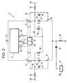
Nach Fig. 2 besitzt der Lichtsender 11 zwei Laserdioden 18, 19, von denen die eine die Meßstrecke 14 und die andere die Referenzstrecke 15 mit einem gebündelten Lichtstrahl versorgt.2, the
Nach Fig. 2 sind die Laserdioden 18, 19 mit ihren Pluspolen über jeweils einen Hilfsschalter 21, 22 mit zugeordnetem Regler bei 23 an eine positive Speisegleichspannungsquelle mit einer Spannung von beispielsweise +5,2 V angeschlossen.2, the
Die negativen Pole der Laserdioden 18, 19 sind über einen Hochfrequenzschalter 24 bzw. 25 an eine geerdete Induktivität 33 angelegt, die Teil eines Hochpasses bildet, zu dem auch ein Kondensator 34 gehört, der von schematisch angedeuteten Hochfrequenz-Modulationsspannungsklemmen 26, 27 beaufschlagt ist, denen die Wellenzugsignale P (Fig.1) zugeführt werden.The negative poles of the
An den positiven Pol der Laserdioden 18, 19 ist über jeweils einen hochohmigen Widerstand 29 bzw. 30 und eine Klemme 28 eine negative Hilfsspannung von z.B. -12 V angeschlossen.At the positive pole of the
Die Hilfsschalter mit Regelung 21, 22 werden über an Klemmen ![]()
![]()
![]()
![]()
Jeder Laserdiode 18, 19 ist eine Monitordiode 18' bzw. 19' zugeordnet, die abwechselnd einen PI-Regler 41 ansteuern, dem außerdem von den Schaltklemmen ![]()
![]()
![]()
![]()
Der PI-Regler 41 gibt bei 94, 95 Regelsteuersignale für den Regelteil der Schalter 21, 22 ab. Auf diese Weise kann der Strom zu den Laserdioden 18, 19 so eingeregelt werden, daß die Lichtintensität der Laserdioden 18, 19 konstant ist. Über die Sollwertzuführung S1, S2 kann weiter dafür gesorgt werden, daß einer Degradation der Laserdioden 18, 19 durch eine stärkere Öffnung der Regler der Schalter 21, 22 entgegengewirkt wird. Auch Voreinstellungen bestimmter Lichtintensitäten sind durch eine Veränderung der Sollwerte S1 und S2 möglich.The
Kondensatoren 35, 37 zwischen den Pluspolen der Laserdioden 18, 19 und Masse stellen einen Hochpaß für die über die Diodenschalter 24, 25 zugeführte Hochfrequenz-Modulationsspannung dar.
Die Schaltung nach Fig. 2 arbeitet wie folgt:The circuit according to FIG. 2 works as follows:
Über die Schaltklemmen 18, 19 werden Schaltsignale für die Schalter 21, 22 in der Weise zugeführt, daß stets der eine Schalter geschlossen, der andere offen ist. Synchron damit werden auch die Hochfrequenzschalter 24, 25 geschlossen bzw. geöffnet, was durch gestrichelte Kopplungslinien 96, 97 angedeutet ist. Sofern die Schalter 21, 24 (siehe linke Darstellung in Fig. 2) geschlossen sind, liegt die zugeordnete Laserdiode 18 zwischen der positiven Speisespannungsklemme 23 und Masse und wird daher eingeschaltet. Über den Hochpaß 33, 34, 35 wird gleichzeitig der durch die Laserdiode 18 fließende Gleichstrom mit einer entsprechenden Hochfrequenzspannung von z.B. 75 MHz moduliert.Switching signals for the
Nachdem auf diese Weise viele Lichtwellenzüge geeigneter Länge über die Meßstrecke 14 zur Empfangsdiode 20 (Fig.1) geschickt worden sind, schaltet das Schaltsignal an der Schaltklemme ![]()
![]()
![]()
![]()
Je nachdem, welche Laserdiode (18 oder 19) aktiv ist, gibt die zugeordnete Monitordiode 18' oder 19' über eine gemeinsame Leitung 98 ein Istwert-Signal an den PI-Regler 41 ab. Gleichzeitig sorgen die Schaltsignale an den Schaltklemmen ![]()
![]()
![]()
![]()
Ein nach dem Prinzipschaltbild der Fig. 2 arbeitendes Schaltungsbeispiel wird im folgenden anhand von Fig. 3 erläutert.A circuit example operating according to the basic circuit diagram of FIG. 2 is explained below with reference to FIG. 3.
Die beiden Laserdioden 18, 19 sind einerseits über einen Schalt-Regeltransistor 21 bzw. 22 und einen in dessen Emitterkreis eingeschalteten Widerstand 50, 51 an die auf einem Potential von +5,2 V liegende positive Speisegleichspannungsklemme 23 angelegt. Der negative Pol der Laserdioden 18, 19 ist andererseits über jeweils eine einen Hochfrequenzschalter bildende in der gleichen Richtung wie die Laserdioden 18, 19 eingeschaltete Schaltdiode 24 bzw. 25 und eine gemeinsame Induktivität 32 an Masse angelegt, deren Potential über eine Klemme 52 zugeführt ist.The two
Die Induktivität 33 ist Bestandteil eines auch einen Kondensator 34 aufweisenden Hochpaßfilters, welches über einen Widerstand 53 an eine Modulationstreiberstufe 54 angeschlossen ist, die aus zwei mittels der Basen miteinander verbundenen Transistoren und den zugeordneten Widerständen besteht und ebenfalls zwischen Masse und die Speisegleichspannungsklemme 23 geschaltet ist. Ein Kondensator 55 sowie eine Induktivität 56 bewirken eine Fernhaltung der Hochfrequenzmodulationsspannung von der Speisegleichspannungsleitung. An den Emitter des einen Transistors der Treiberstufe 54 ist über einen Widerstand 57 und einen Kondensator 58 die Ausgangsspannung eines Übertragers 59 angeschlossen, dessen Eingangswicklung über ein Potentiometer 60 an die Hochfrequenz-Modulationsspannungsklemmen 26, 27 angelegt ist, der die Wellenzugsignale P (Fig.1) zugeführt sind. Die positive Zuleitung zu den Laserdioden 18, 19 ist über Hochfrequenz-Ableitungskondensatoren 35, 36 bzw. 37, 38 an Masse und über hochohmige Widerstände 29 bzw. 30 an eine Klemme 28 für die Zuführung einer Hilfsspannung von -12 V angelegt.The
Der Verbindungspunkt zwischen den Laserdioden 18, 19 und den zugeordneten Schaltdioden 24, 25 ist über eine entgegen den Laserdioden 18, 19 geschaltete Hilfsdiode 61 bzw. 62 ebenfalls an die positive Zuleitung der Laserdioden 18, 19 angeschlossen. Der von den Transistoren 21, 22 abgewandte Pol der Hilfsdioden 61, 62 ist außerdem über einen Widerstand 63, 64 geerdet.The connection point between the
Jeder Laserdiode 18, 19 ist eine Monitordiode 18', 19' zugeordnet, die einerseits an die positive Zuleitung und andererseits über in der gleichen Richtung wie die Dioden 24, 25 eingeschaltete Dioden 39, 40 gemeinsam an den Eingang des PI-Reglers 41 angelegt sind, welcher zwei hintereinandergeschaltete Operationsverstärker 65 bzw. 66 enthält. Die Betriebsspannungen werden in der dargestellten Weise von der auf -12 V liegenden Klemme 28 und einer weiteren auf +12 V liegenden Klemme 67 abgeleitet. Der Minus-Eingangsklemme des Operationsverstärkers 66 werden abwechselnd zwei Sollsignale S1, S2 zugeführt, die über parallel geschaltete Sollwert-Einstellungspotentiometer 68 bzw. 69 und Schalttransistoren 70 bzw. 71 von einer eine exakte Konstantgleichspannung führenden Klemme 42 abgeleitet sind. Die Gleichspannung wird den Potentiometern 68, 69 über Schalttransistoren 70, 71 zugeführt, die von den bei ![]()
![]()
![]()
![]()
Der Ausgang des PI-Reglers 41 ist über Widerstände 72 bzw. 73 dem Kollektor eines Schalttransistors 31 bzw. 32 zugeführt, der über eine Diode 74 bzw. 75 in der dargestellten Weise an die positive Versorgungsgleichspannung +5,2 V angelegt ist. Die positive Speisegleichspannungsleitung ist über einen Kondensator 76 zur weiteren Hochfrequenzentkopplung geerdet.The output of the
Dem Kollektor der Schalttransistoren 31 bzw. 32 wird jeweils über einen Widerstand 77 bzw. 78 von den Klemmen ![]()
![]()
![]()
![]()
Die Emitter der Schalttransistoren 31, 32 sind über Kondensatoren 79 bzw. 80 und Widerstände 81 bzw. 82 an die positive Gleichspannungsklemme 23 angelegt. Weiter ist er mit der Basis des Transistors 21 bzw. 22 verbunden, dessen Emitter wie oben bereits erwähnt über einen Widerstand 50 bzw. 51 an der positiven Speisegleichspannung +5,2 V liegt und dessen Kollektor mit der positiven Zuleitung für die Laserdioden 18 bzw. 19 verbunden ist.The emitters of the switching
Von den Emittern der Regel-Schalttransistoren 21 bzw. 22 wird über Widerstände 83 bzw. 84 eine Spannung abgegriffen und zu einer Klemme 85 geführt. Dieses Signal ist für den durch die Laserdioden 18, 19 fließenden Strom repräsentativ und kann im Mikroprozessor 16 (Fig. 1) zur Überwachung des Regelkreises bezüglich Einhaltung der Laserschutzklasse oder der Degradation beider Laser herangezogen werden. Zu diesem Zweck ist auch eine weitere Überwachungsklemme 86 vorgesehen, die über einen Widerstand 87 an den Ausgang des Operationsverstärkers 65 des PI-Reglers 41 angelegt ist. Da dieses Signal von der Lichtbeaufschlagung der Monitordioden 18', 19' abhängig ist, ist es repräsentativ für die Helligkeit der Laserdioden 18, 19 bei einem bestimmten angelegten Strom, der wiederum an der Klemme 85 gemessen werden kann. Auf diese Weise kann der Mikroprozessor 16, an den die Klemmen 85, 86 angeschlossen sind, feststellen, wenn beispielsweise für einen bestimmten Diodenstrom die Lichtleistung nachläßt, was dann bei der Auswertung Berücksichtigung finden kann.A voltage is tapped from the emitters of the
Die Funktion der beschriebenen Schaltung ist wie folgt:The function of the circuit described is as follows:
Über die Laserdioden-Schaltklemmen ![]()
![]()
![]()
![]()
Aufgrund der den Widerständen 29 bzw. 30 zugeführten negativen Spannung von -12 V ist jeweils nur diejenige Schaltdiode 24 oder 25 geöffnet, deren Laserdiode 18 oder 19 über den zugeordneten Transistor 21 oder 22 eine positive Spannung zugeführt ist. Hierdurch entfällt nämlich der von der negativen Spannung durch die Dioden 61 bzw. 62 und die Widerstände 63 bzw. 64 gezogenen Strom, welcher den positiven Pol der Schalttransistoren 24 oder 25 negativ gemacht hatte, so daß die betreffende Schaltdiode sperrte. Die Schaltdioden 24, 25 öffnen und schließen also synchron mit den zugehörigen Laserdioden 18, 19.Because of the negative voltage of -12 V supplied to the
Sobald eine Laserdiode z.B. 18 aktiv ist, kann über die nunmehr offene Schaltdiode, z.B. 24, vom Hochpaß 33, 34 her die bei 26, 27 angelegte Hochfrequenz-Modulationsspannung zu der zugeordneten Laserdiode, z.B. 18, gelangen. Sie wird über die Kondensatoren 35, 36 oder 37, 38 nach Masse abgeführt. Auf diese Weise erfolgt die Modulation der Laserdioden 18, 19, während sie von einer sie zum Leuchten bringenden Gleichspannung beaufschlagt sind. Die Modulationstiefe ist so groß, daß die Dioden während der Modulation in Rhythmus der zugeführten Hochfrequenz-Modulationsspannung erlöschen und wieder aufleuchten und kann am Potentiometer 60 eingestellt werden.As soon as a laser diode e.g. 18 is active, can be activated via the now open switching diode, e.g. 24, from high-
Aufgrund des Anschlusses des Kollektors der Transistoren 31, 32 an den Ausgang des PI-Reglers 41 wird der Öffnungsgrad der Regel-Schalttransistoren 21 bzw. 22 gerade so eingeregelt, daß die Laserdioden 18 bzw. 19 die an den Potentiometern 68 bzw. 69 eingestellte Lichtstärke annehmen. Die Regel-Schalttransistoren 21, 22 erfüllen also eine Doppelfunktion als Stellglieder des Regelkreises wie auch als Schalter für die Zu- und Abschaltung der Laserdioden 18, 19. Erfindungsgemäß führen also die Schaltdioden 24, 25 sowohl den Gleich-Laserstrom als auch den überlagerten Modulations-Hochfrequenzstrom. Es handelt sich um Hochfrequenzschalter, weil sie beim Abschalten der zugeordneten Laserdiode 18 oder 19 öffnen und beim Zuschalten von selbst wieder schließen.Due to the connection of the collector of the
Wesentlich ist auch noch, daß bei abgeschalteten Laserdioden 18 bzw. 19 die positiven Zuleitungen die Laserdioden über die Widerstände 29, 30 an eine negative Hilfsspannung angelegt sind, so daß in diesen Perioden eine die Laserdioden vollständig sperrende Spannung an ihnen anliegt. Im abgeschalteten Zustand der Laserdioden 18 oder 19 liegt jeweils ein Spannungsteiler über den Widerstand 63, die Diode 61 und den Widerstand 29 bzw. den Widerstand 64, die Diode 62 und den Widerstand 30 vor. Die Dioden 61, 62 begrenzen diese Hilfsspannung auf einen zulässigen Wert. Dadurch werden die gewünschten Eigenschaften, nämlich insbesondere das Aufleuchten der Laserdioden nur in den gewünschten Perioden unterstützt.It is also essential that when the
Die Helligkeit der beiden Laserdioden kann durch die Potentiometer 68 oder 69 voreingestellt werden.The brightness of the two laser diodes can be preset using
Die Regelbandbreite des PI-Reglers 41 ist sehr viel kleiner als die Modulationsfrequenz.The control bandwidth of the
Während jeder Einschaltperiode einer der Laserdioden 18, 19 werden einige tausend hochfrequenzmodulierte Lichtwellenzüge über die Meßstrecke 14 bzw. die Referenzstrecke 15 übertragen.During each switch-on period of one of the
Claims (13)
- Distance measuring apparatus comprising a photoelectric light receiver (12) and a photoelectric light transmitter (11) which is preferably arranged alongside the photoelectric light receiver which alternately transmits high frequency modulated light wave trains to the light receiver (12) via a measurement path (14) and a reflective target arranged at its end, wherein the distance of the target from the light transmitter (11) / light receiver (12) is to be measured, and via a reference path (15) of known length provided between the light transmitter (11) and the light receiver (12), preferably within the housing (17); and also comprising an electronic evaluation circuit which preferably contains a microprocessor (16) and which evaluates the light wave trains which are alternately received by the light receiver (12) with respect to the difference of the transit time via the measurement path (14), on the one hand, and the transit time via the reference path (15), on the other hand, and which deduces from this the distance of the light transmitter (11) / light receiver (12) from the target (13), taking account of the speed of light and the known length of the reference path (15), wherein the light transmitter (11) contains two opto-electronic light transmitter elements, in particular semiconductor light transmitter elements and preferably laser diodes (18, 19), which can be switched electronically in a complementary manner, of which the one light transmitter element (18) transmits the light wave trains via the measurement path (14) and the other (19) transmits the light wave trains via the reference path (14); and wherein the light receiver (12) contains an opto-electronic light receiving element, in particular a light receiving semiconductor element, preferably a photodiode element (20) which is connected to the electronic processing circuit, characterised in that the light wave trains emitted from the light transmitter (11) and transmitted by an oscillator arrangement (43, 44, 45, 46) are high frequency modulated; in that the light receiving element (20) is connected to the one input of a multiplicatively operating mixing stage (47) of the electronic evaluation circuit, with the one output wave train signal (P') of a digital phase shifter (46) being applied to the other input of the electronic evaluation circuit, the phase shifter producing four phase pairs timewise one after the other, which are settable in a 90° grid and each have the modulation frequency, with the other output wave signal (P) being passed on further to the light transmitter (11); in that a particularly narrow band approximation filter which forms the integral (PxP') of the output product of the two output wave train signals is connected to the output of the mixing stage (47), with the output signals appearing at the output of the approximation filter (48) being evaluated in the microprocessor (16) contained in the electronic evaluation circuit to find the difference of the transit times of the light wave train via the measurement path (14) on the one hand and via the reference path (15) on the other hand.
- Distance measuring apparatus in accordance with claim 1, characterised in that the laser diodes (18, 19) can be connected to a DC feed voltage (23) by auxiliary switches (21, 22) which can be switched in a complementary manner and can be connected to the high frequency modulation voltage (26, 27) by high frequency switches (24, 25) which can be switched in a complementary manner, preferably in synchrony with the auxiliary switches (21, 22).
- Distance measuring apparatus in accordance with claim 2, characterised in that the auxiliary switches (21, 22) are inserted into the positive feed lines and the high frequency switches (24, 25) are inserted into the negative feedlines to the laser diodes (18; 19).
- Distance measuring apparatus in accordance with claim 2 or claim 3, characterised in that a preferably negative potential (28) is applied to the respectively switched off laser diode (18; 19) in the depletion direction.
- Distance measuring apparatus in accordance with claim 4, characterised in that the positive terminal of each laser diode (18; 19) is connected to a preferably negative DC blocking potential (28) via a resistance (29; 30) which is of a higher order of magnitude than the resistance value of the through switched laser diode (18; 19).
- Distance measuring apparatus in accordance with one of the claims 2 to 5, characterised in that the positive terminal of each laser diode (18; 19) is connected to the positive feed voltage (23) via a respective transistor (21, 22) which forms the auxiliary switch.
- Distance measuring apparatus in accordance with claim 6, characterised in that the transistor (21; 22) is acted on both by a switching signal


- Distance measuring apparatus in accordance with claim 7, characterised in that a switching transistor (31; 32) which is preferably acted on at its base by the switching signal (


- Distance measuring apparatus in accordance with claim 8 to 9, characterised in that switching diodes (24; 25) which are poled in the same direction as the laser diodes (18; 19) are inserted into the negative feedline to the laser diodes (18; 19) as high frequency switches and are jointly connected via the inductor (33) of a high pass filter (33, 34) energised by the high frequency modulation potential (26, 27) to the negative pole of the feed voltage or to earth.
- Distance measuring apparatus in accordance with claim 9, characterised in that the connection point of each switching diode (24; 25) to the laser diode (18; 19) lies at a negative potential (28) when the laser diode (18; 19) is switched off.
- Distance measuring apparatus in accordance with claims 9 or 10, characterised in that high frequency decoupling capacitors (35, 36, 37, 38) are inserted between the positive feedline to the laser diodes (18, 19) and the negative pole of the feed voltage or earth.
- Distance measuring apparatus in accordance with one of the claims 2 to 11, characterised in that a preferably integrated monitoring diode (18'; 19') is associated with each laser diode (18, 19), with the monitoring diode preferably being connected via a diode (39, 40) poled in the same direction as the switching diodes (24, 25) to the input of a PI-regulator (41), which preferably regulates the laser diodes (18, 19) to a predetermined intensity value via the switching regulating transistors (21, 22; 31, 32).
- Distance measuring apparatus in accordance with claim 12, characterised in that a desired value signal which takes account of the degradation of the laser diodes (18; 19), or which serves for the adjustment of the laser diode brightness, is also supplied to the PI regulator (41); and indeed in that a separate desired value signal (S1, S2) is preferably provided for each laser diode (18, 19).
Applications Claiming Priority (2)
| Application Number | Priority Date | Filing Date | Title |
|---|---|---|---|
| DE4002356 | 1990-01-26 | ||
| DE4002356A DE4002356C2 (en) | 1990-01-26 | 1990-01-26 | Distance measuring device |
Publications (3)
| Publication Number | Publication Date |
|---|---|
| EP0439011A2 EP0439011A2 (en) | 1991-07-31 |
| EP0439011A3 EP0439011A3 (en) | 1993-01-20 |
| EP0439011B1 true EP0439011B1 (en) | 1997-03-26 |
Family
ID=6398873
Family Applications (1)
| Application Number | Title | Priority Date | Filing Date |
|---|---|---|---|
| EP91100115A Expired - Lifetime EP0439011B1 (en) | 1990-01-26 | 1991-01-02 | Distance measurement device |
Country Status (4)
| Country | Link |
|---|---|
| US (1) | US5180922A (en) |
| EP (1) | EP0439011B1 (en) |
| JP (1) | JP3188282B2 (en) |
| DE (2) | DE4002356C2 (en) |
Cited By (1)
| Publication number | Priority date | Publication date | Assignee | Title |
|---|---|---|---|---|
| DE10259135A1 (en) * | 2002-12-18 | 2004-07-01 | Conti Temic Microelectronic Gmbh | Method and arrangement for referencing 3D imagers |
Families Citing this family (52)
| Publication number | Priority date | Publication date | Assignee | Title |
|---|---|---|---|---|
| DE4124192A1 (en) * | 1991-07-20 | 1993-01-21 | Dornier Luftfahrt | Optical rangefinder for spacing between moving road vehicles - measures propagation time of infrared reflection from preceding vehicle, and gives warning of too near approach |
| WO1993020458A2 (en) * | 1992-03-30 | 1993-10-14 | Imatronic Limited | Laser distance measurement |
| DE4304290C1 (en) * | 1993-02-12 | 1994-03-03 | Sick Optik Elektronik Erwin | EM wave, esp. light, transition time measuring appts. - transmits light pulses over measurement path to receiver, has pulse generator and light modulator in feedback path. |
| DE4316348A1 (en) * | 1993-05-15 | 1994-11-17 | Wild Heerbrugg Ag | Distance measuring device |
| DE4320485B4 (en) * | 1993-06-21 | 2007-04-19 | Eads Deutschland Gmbh | Object measuring method by means of intelligent distance image camera |
| DE4411218C1 (en) * | 1994-02-25 | 1995-09-07 | Rudolf Prof Dr Ing Schwarte | Rangefinder operating on propagation time principle |
| DE19517001A1 (en) * | 1995-05-09 | 1996-11-14 | Sick Optik Elektronik Erwin | Method and device for determining the light propagation time over a measuring section arranged between a measuring device and a reflecting object |
| DE19520993A1 (en) * | 1995-06-08 | 1996-12-12 | Sick Optik Elektronik Erwin | Distance measuring method and device |
| US5867125A (en) * | 1995-12-20 | 1999-02-02 | Cluff; Larry A. | Incremental phase and distance measurement through digital phase signature comparison |
| DE19643287A1 (en) * | 1996-10-21 | 1998-04-23 | Leica Ag | Method and device for calibrating distance measuring devices |
| US5852410A (en) * | 1997-03-04 | 1998-12-22 | Maxtec International Corporation | Laser optical path degradation detecting device |
| US6459483B1 (en) | 1998-02-10 | 2002-10-01 | Toolz, Ltd. | Level with angle and distance measurement apparatus |
| DE19840049C5 (en) | 1998-09-02 | 2007-11-08 | Leica Geosystems Ag | Device for optical distance measurement |
| US6563105B2 (en) * | 1999-06-08 | 2003-05-13 | University Of Washington | Image acquisition with depth enhancement |
| DE10006493C2 (en) * | 2000-02-14 | 2002-02-07 | Hilti Ag | Method and device for optoelectronic distance measurement |
| DE10010212A1 (en) * | 2000-03-02 | 2001-09-13 | Sick Ag | Device for determining the light transit time |
| DE10027239A1 (en) * | 2000-05-31 | 2001-12-06 | Sick Ag | Distance measuring method and distance measuring device |
| DE50114296D1 (en) * | 2000-07-27 | 2008-10-23 | Leuze Electronic Gmbh & Co Kg | Optoelectronic device |
| EP1191697B1 (en) * | 2000-07-31 | 2011-12-21 | HILTI Aktiengesellschaft | Local Oscillator for the Generation of an HF-Signal to be Directly Mixed by Avalanche-Photodiodes |
| EP1388739A1 (en) * | 2002-08-09 | 2004-02-11 | HILTI Aktiengesellschaft | Laser range finder with phase difference measurement |
| EP1450128A1 (en) | 2003-02-19 | 2004-08-25 | Leica Geosystems AG | Method and device for extracting geodesic distance information |
| US7006203B1 (en) | 2003-08-21 | 2006-02-28 | United States Of America As Represented By The Administrator Of The National Aeronautics And Space Administration | Video guidance sensor system with integrated rangefinding |
| DE10350489B4 (en) * | 2003-10-29 | 2005-10-13 | Leuze Electronic Gmbh & Co Kg | Optical sensor |
| KR100710683B1 (en) * | 2004-05-12 | 2007-04-24 | 주식회사 탑 엔지니어링 | Sealant dispenser |
| DE102004031097B4 (en) * | 2004-06-28 | 2012-02-09 | Diehl Bgt Defence Gmbh & Co. Kg | laser measuring device |
| WO2007033608A1 (en) * | 2005-09-26 | 2007-03-29 | Hongkong Applied Science And Technology Research Institute Co., Ltd. | Optical receiver with a modulated photo-detector |
| US7592615B2 (en) * | 2005-10-11 | 2009-09-22 | Hong Kong Applied Science And Technology Research Institute Co., Ltd. | Optical receiver with a modulated photo-detector |
| JP4260852B2 (en) * | 2006-05-24 | 2009-04-30 | シャープ株式会社 | Optical distance measuring device and manufacturing method thereof |
| DE102006034926A1 (en) | 2006-07-28 | 2008-01-31 | Sick Ag | Opto-electronic distance measuring device for determining distance of object, comprises illuminating unit and transceiver optics with beam forming optics, where transceiver optics produces different illuminating patterns on objects |
| US8600290B2 (en) * | 2007-06-05 | 2013-12-03 | Lockheed Martin Corporation | Hybrid band directed energy target disruption |
| JP5051525B2 (en) * | 2007-06-05 | 2012-10-17 | 学校法人日本大学 | Displacement measurement system |
| JP5202097B2 (en) * | 2008-05-14 | 2013-06-05 | 株式会社キーエンス | Optical scanning photoelectric switch |
| JP5156475B2 (en) * | 2008-05-14 | 2013-03-06 | 株式会社キーエンス | Optical scanning photoelectric switch |
| JP5036624B2 (en) * | 2008-05-20 | 2012-09-26 | 株式会社キーエンス | Monitoring area setting device |
| JP5096235B2 (en) * | 2008-06-03 | 2012-12-12 | 株式会社キーエンス | Area monitoring sensor |
| JP5086899B2 (en) * | 2008-06-03 | 2012-11-28 | 株式会社キーエンス | Area monitoring sensor |
| US8948607B2 (en) * | 2008-10-09 | 2015-02-03 | Finisar Corporation | Active linear amplifier inside transmitter module |
| US8415609B2 (en) | 2009-01-31 | 2013-04-09 | Keyence Corporation | Safety photoelectric switch |
| JP5473044B2 (en) * | 2009-01-31 | 2014-04-16 | 株式会社キーエンス | Safety photoelectric switch |
| JP2010175488A (en) * | 2009-01-31 | 2010-08-12 | Keyence Corp | Optical scan type photoelectric switch |
| DE102009019871B4 (en) | 2009-05-06 | 2011-02-03 | Konrad Maierhofer | Auxiliary device for the fine adjustment of a laser beam to a predefinable target point |
| DE102010013751A1 (en) | 2010-03-31 | 2011-10-06 | Baumer Innotec Ag | Device for measuring distance between transceiver and target in industrial application, has evaluating device scanning light pulses with respect to phase shifts, where pulses are transmitted by transmitter at certain pulse repetition rate |
| JP5840209B2 (en) * | 2011-07-27 | 2016-01-06 | ジックオプテックス株式会社 | Lightwave ranging device |
| DE102011081568B3 (en) * | 2011-08-25 | 2012-09-27 | Ifm Electronic Gmbh | Optical receiver for light transit time apparatus e.g. photonic mixer device, has photo detector connected with reference potential over input resistance of current-voltage converter, and smoothing capacitor for smoothing photocurrent |
| EP2607924A1 (en) | 2011-12-23 | 2013-06-26 | Leica Geosystems AG | Distance sensor adjustment |
| DE102012200152A1 (en) * | 2012-01-05 | 2013-07-11 | Robert Bosch Gmbh | Device and method for measuring a camera |
| DE102013102745B4 (en) * | 2013-03-18 | 2018-02-15 | Leuze Electronic Gmbh + Co. Kg | Optical sensor |
| EP3415944A1 (en) | 2017-06-16 | 2018-12-19 | Leuze electronic GmbH + Co. KG | Optical sensor |
| DE102018222049A1 (en) * | 2018-12-18 | 2020-06-18 | Ibeo Automotive Systems GmbH | Device for operating a light source for optical transit time measurement |
| JPWO2022219912A1 (en) * | 2021-04-12 | 2022-10-20 | ||
| DE102022201070B4 (en) | 2022-02-01 | 2023-10-12 | Universität Paderborn, Körperschaft des öffentlichen Rechts | Electro-optical mixer |
| EP4231047A1 (en) * | 2022-02-18 | 2023-08-23 | Sick Ag | Optoelectronic sensor for detecting and determining the distance of objects and trigger circuit for such a sensor |
Family Cites Families (16)
| Publication number | Priority date | Publication date | Assignee | Title |
|---|---|---|---|---|
| GB993072A (en) * | 1963-03-21 | 1965-05-26 | Ferranti Ltd | Improvements relating to measuring apparatus |
| US3428815A (en) * | 1965-10-22 | 1969-02-18 | Electronic Ind Eng Inc | Distance measuring system using infrared ring-around oscillator with a reference loop having a light conducting rod |
| US3522992A (en) * | 1967-06-28 | 1970-08-04 | North American Rockwell | Geodetic survey system and digital phase-meter therefor |
| FR2081184B1 (en) * | 1970-03-16 | 1974-05-24 | Comp Generale Electricite | |
| GB1585054A (en) * | 1975-02-14 | 1981-02-25 | Secr Defence | Laser rangefinder |
| US4102572A (en) * | 1977-08-11 | 1978-07-25 | Hughes Aircraft Company | Dual-wavelength coherent optical adaptive systems |
| DE2921110A1 (en) * | 1979-05-25 | 1980-12-04 | Leuze Electronic Kg | Light-electrical arrangement with light transmitter and receiver - has partially-transmissive mirror inclined to beam path of transmitter and auxiliary transmitter or receiver |
| GB2066015B (en) * | 1979-10-23 | 1984-02-15 | South African Inventions | Distance measurment |
| DE3103567A1 (en) * | 1981-02-03 | 1982-08-12 | MITEC Moderne Industrietechnik GmbH, 8012 Ottobrunn | DISTANCE MEASURING METHOD ACCORDING TO THE PRINCIPLE OF THE RUNTIME MEASUREMENT OF A MEASURING LIGHT IMPULSE AND DEVICE FOR ITS IMPLEMENTATION |
| DE3219423C2 (en) * | 1981-06-09 | 1986-04-30 | MTC, Meßtechnik und Optoelektronik AG, Neuenburg/Neuchâtel | Distance measuring method and device for its implementation |
| JPS5838880A (en) * | 1981-08-31 | 1983-03-07 | Tokyo Optical Co Ltd | Light wave range finder |
| JPS58174874A (en) * | 1982-04-08 | 1983-10-13 | Tokyo Optical Co Ltd | Light wave distance measuring method and apparatus |
| DE3429062A1 (en) * | 1984-08-07 | 1986-02-20 | Erwin Sick Gmbh Optik-Elektronik, 7808 Waldkirch | DEVICE FOR MEASURING THE RUNNING TIME OF ELECTROMAGNETIC SHAFTS |
| US4895441A (en) * | 1987-03-19 | 1990-01-23 | Pandel Instruments, Inc. | Method and apparatus for precision ranging |
| JPS63280482A (en) * | 1987-05-12 | 1988-11-17 | Nec Corp | Optical transmission circuit |
| JP2896782B2 (en) * | 1988-12-30 | 1999-05-31 | 株式会社トプコン | Pulse type lightwave distance meter |
-
1990
- 1990-01-26 DE DE4002356A patent/DE4002356C2/en not_active Expired - Fee Related
-
1991
- 1991-01-02 EP EP91100115A patent/EP0439011B1/en not_active Expired - Lifetime
- 1991-01-02 DE DE59108629T patent/DE59108629D1/en not_active Expired - Fee Related
- 1991-01-22 US US07/643,862 patent/US5180922A/en not_active Expired - Lifetime
- 1991-01-28 JP JP09179591A patent/JP3188282B2/en not_active Expired - Fee Related
Cited By (1)
| Publication number | Priority date | Publication date | Assignee | Title |
|---|---|---|---|---|
| DE10259135A1 (en) * | 2002-12-18 | 2004-07-01 | Conti Temic Microelectronic Gmbh | Method and arrangement for referencing 3D imagers |
Also Published As
| Publication number | Publication date |
|---|---|
| JPH07229966A (en) | 1995-08-29 |
| US5180922A (en) | 1993-01-19 |
| EP0439011A2 (en) | 1991-07-31 |
| DE59108629D1 (en) | 1997-04-30 |
| EP0439011A3 (en) | 1993-01-20 |
| DE4002356C1 (en) | 1991-02-28 |
| JP3188282B2 (en) | 2001-07-16 |
| DE4002356C2 (en) | 1996-10-17 |
Similar Documents
| Publication | Publication Date | Title |
|---|---|---|
| EP0439011B1 (en) | Distance measurement device | |
| EP0057447B1 (en) | Distance measuring apparatus according to the principles of the travel time measurement of a light pulse | |
| EP1936400B1 (en) | Laser scanner | |
| DE10022054B4 (en) | Optical distance sensor | |
| EP0010064A1 (en) | Method of electro-optical distance measurement and apparatus for carrying out the method | |
| DE2422139A1 (en) | DIGITAL OBJECT SCANNING DEVICE | |
| WO2013170982A1 (en) | Optical distance measurement device with calibration device to take cross-talk into account | |
| DE19643287A1 (en) | Method and device for calibrating distance measuring devices | |
| EP0742450A2 (en) | Method and apparatus for measuring the time for light to travel a measurement path extending between a measurement apparatus and a reflecting object | |
| DE10235562A1 (en) | Optical distance measurement device has a measurement diode, which is used for reflected signal detection and frequency conversion to a lower frequency, that has high frequency modulated electrode voltages | |
| EP0010682A1 (en) | Device for transmitting analogue signals over an optical link | |
| DE2401906C3 (en) | Device for measuring visibility in a measurement area | |
| EP0050306A2 (en) | Fibre-optics measuring instrument | |
| DE2848148A1 (en) | RADAR WITH CONTINUOUS VIBRATION | |
| EP0173155A2 (en) | Power supply for the light sources of frequency-modulated optical detectors | |
| DE3022857A1 (en) | DEVICE FOR MEASURING TIME | |
| DE4328553A1 (en) | Rangefinder using the propagation time principle | |
| EP0323871A2 (en) | Voltage to frequency converter and its application in a fibre optic transmission system | |
| EP3508874A1 (en) | Calibrating device for a tof camera device | |
| EP0383352A1 (en) | Sensor for an automatically steered vehicle | |
| EP1585234A1 (en) | Photoelectronic Mixing Device (PMD) system and method for operating a PMD | |
| DE102017206672B4 (en) | Circuit for operating a light source | |
| DE102015117246A1 (en) | Optical fiber arrangement for optical drop detection | |
| EP0280261A2 (en) | Circuit for getting a temperature independent rectangular signal from a measuring signal | |
| EP0139109A1 (en) | Device to determine time delay variations |
Legal Events
| Date | Code | Title | Description |
|---|---|---|---|
| PUAI | Public reference made under article 153(3) epc to a published international application that has entered the european phase |
Free format text: ORIGINAL CODE: 0009012 |
|
| AK | Designated contracting states |
Kind code of ref document: A2 Designated state(s): DE FR GB IT NL |
|
| PUAL | Search report despatched |
Free format text: ORIGINAL CODE: 0009013 |
|
| AK | Designated contracting states |
Kind code of ref document: A3 Designated state(s): DE FR GB IT NL |
|
| 17P | Request for examination filed |
Effective date: 19930317 |
|
| 17Q | First examination report despatched |
Effective date: 19941202 |
|
| GRAG | Despatch of communication of intention to grant |
Free format text: ORIGINAL CODE: EPIDOS AGRA |
|
| GRAH | Despatch of communication of intention to grant a patent |
Free format text: ORIGINAL CODE: EPIDOS IGRA |
|
| GRAH | Despatch of communication of intention to grant a patent |
Free format text: ORIGINAL CODE: EPIDOS IGRA |
|
| RAP1 | Party data changed (applicant data changed or rights of an application transferred) |
Owner name: SICK AG |
|
| GRAA | (expected) grant |
Free format text: ORIGINAL CODE: 0009210 |
|
| ITF | It: translation for a ep patent filed |
Owner name: BARZANO' E ZANARDO MILANO S.P.A. |
|
| AK | Designated contracting states |
Kind code of ref document: B1 Designated state(s): DE FR GB IT NL |
|
| PG25 | Lapsed in a contracting state [announced via postgrant information from national office to epo] |
Ref country code: NL Free format text: LAPSE BECAUSE OF FAILURE TO SUBMIT A TRANSLATION OF THE DESCRIPTION OR TO PAY THE FEE WITHIN THE PRESCRIBED TIME-LIMIT Effective date: 19970326 |
|
| GBT | Gb: translation of ep patent filed (gb section 77(6)(a)/1977) |
Effective date: 19970327 |
|
| REF | Corresponds to: |
Ref document number: 59108629 Country of ref document: DE Date of ref document: 19970430 |
|
| ET | Fr: translation filed | ||
| NLV1 | Nl: lapsed or annulled due to failure to fulfill the requirements of art. 29p and 29m of the patents act | ||
| PLBE | No opposition filed within time limit |
Free format text: ORIGINAL CODE: 0009261 |
|
| STAA | Information on the status of an ep patent application or granted ep patent |
Free format text: STATUS: NO OPPOSITION FILED WITHIN TIME LIMIT |
|
| 26N | No opposition filed | ||
| PGFP | Annual fee paid to national office [announced via postgrant information from national office to epo] |
Ref country code: GB Payment date: 19990105 Year of fee payment: 9 |
|
| PG25 | Lapsed in a contracting state [announced via postgrant information from national office to epo] |
Ref country code: GB Free format text: LAPSE BECAUSE OF NON-PAYMENT OF DUE FEES Effective date: 20000102 |
|
| PGFP | Annual fee paid to national office [announced via postgrant information from national office to epo] |
Ref country code: FR Payment date: 20000118 Year of fee payment: 10 |
|
| GBPC | Gb: european patent ceased through non-payment of renewal fee |
Effective date: 20000102 |
|
| PG25 | Lapsed in a contracting state [announced via postgrant information from national office to epo] |
Ref country code: FR Free format text: LAPSE BECAUSE OF NON-PAYMENT OF DUE FEES Effective date: 20010928 |
|
| REG | Reference to a national code |
Ref country code: FR Ref legal event code: ST |
|
| PG25 | Lapsed in a contracting state [announced via postgrant information from national office to epo] |
Ref country code: IT Free format text: LAPSE BECAUSE OF NON-PAYMENT OF DUE FEES;WARNING: LAPSES OF ITALIAN PATENTS WITH EFFECTIVE DATE BEFORE 2007 MAY HAVE OCCURRED AT ANY TIME BEFORE 2007. THE CORRECT EFFECTIVE DATE MAY BE DIFFERENT FROM THE ONE RECORDED. Effective date: 20050102 |
|
| PGFP | Annual fee paid to national office [announced via postgrant information from national office to epo] |
Ref country code: DE Payment date: 20090325 Year of fee payment: 19 |
|
| PG25 | Lapsed in a contracting state [announced via postgrant information from national office to epo] |
Ref country code: DE Free format text: LAPSE BECAUSE OF NON-PAYMENT OF DUE FEES Effective date: 20100803 |