EP0437779B1 - Dat drive/controller interface - Google Patents
Dat drive/controller interface Download PDFInfo
- Publication number
- EP0437779B1 EP0437779B1 EP90124782A EP90124782A EP0437779B1 EP 0437779 B1 EP0437779 B1 EP 0437779B1 EP 90124782 A EP90124782 A EP 90124782A EP 90124782 A EP90124782 A EP 90124782A EP 0437779 B1 EP0437779 B1 EP 0437779B1
- Authority
- EP
- European Patent Office
- Prior art keywords
- data
- read
- tape
- drive
- information
- Prior art date
- Legal status (The legal status is an assumption and is not a legal conclusion. Google has not performed a legal analysis and makes no representation as to the accuracy of the status listed.)
- Expired - Lifetime
Links
Images


Classifications
-
- G—PHYSICS
- G06—COMPUTING; CALCULATING OR COUNTING
- G06F—ELECTRIC DIGITAL DATA PROCESSING
- G06F3/00—Input arrangements for transferring data to be processed into a form capable of being handled by the computer; Output arrangements for transferring data from processing unit to output unit, e.g. interface arrangements
- G06F3/06—Digital input from, or digital output to, record carriers, e.g. RAID, emulated record carriers or networked record carriers
- G06F3/0601—Interfaces specially adapted for storage systems
-
- G—PHYSICS
- G11—INFORMATION STORAGE
- G11B—INFORMATION STORAGE BASED ON RELATIVE MOVEMENT BETWEEN RECORD CARRIER AND TRANSDUCER
- G11B20/00—Signal processing not specific to the method of recording or reproducing; Circuits therefor
- G11B20/10—Digital recording or reproducing
-
- G—PHYSICS
- G06—COMPUTING; CALCULATING OR COUNTING
- G06F—ELECTRIC DIGITAL DATA PROCESSING
- G06F3/00—Input arrangements for transferring data to be processed into a form capable of being handled by the computer; Output arrangements for transferring data from processing unit to output unit, e.g. interface arrangements
- G06F3/06—Digital input from, or digital output to, record carriers, e.g. RAID, emulated record carriers or networked record carriers
- G06F3/0601—Interfaces specially adapted for storage systems
- G06F3/0668—Interfaces specially adapted for storage systems adopting a particular infrastructure
- G06F3/0671—In-line storage system
- G06F3/0673—Single storage device
- G06F3/0682—Tape device
-
- G—PHYSICS
- G11—INFORMATION STORAGE
- G11B—INFORMATION STORAGE BASED ON RELATIVE MOVEMENT BETWEEN RECORD CARRIER AND TRANSDUCER
- G11B20/00—Signal processing not specific to the method of recording or reproducing; Circuits therefor
- G11B20/10—Digital recording or reproducing
- G11B20/12—Formatting, e.g. arrangement of data block or words on the record carriers
-
- G—PHYSICS
- G11—INFORMATION STORAGE
- G11B—INFORMATION STORAGE BASED ON RELATIVE MOVEMENT BETWEEN RECORD CARRIER AND TRANSDUCER
- G11B2220/00—Record carriers by type
- G11B2220/90—Tape-like record carriers
- G11B2220/91—Helical scan format, wherein tracks are slightly tilted with respect to tape direction, e.g. VHS, DAT, DVC, AIT or exabyte
- G11B2220/916—Digital data storage [DDS] format
Definitions
- the disclosed invention is directed generally to computer storage digital audio tape (DAT) drives, and more particularly is directed to an interface between a DAT drive and an associated controller.
- DAT digital audio tape
- DAT Digital audio tape
- DIGITAL AUDIO TAPE RECORDER Digital audio tape
- An example of a format for the storage of computer data utilizing DAT technology is the American National Standards Institute (ANSI) Digital Data Storage (DDS) standard, presently in draft form ("PROPOSED AMERICAN NATIONAL STANDARD HELICAL-SCAN DIGITAL COMPUTER TAPE CARTRIDGE 381 mm (0.150 in) FOR INFORMATION INTERCHANGE," ASC X3 Project No. 668-D).
- ANSI American National Standards Institute
- DDS Digital Data Storage
- the characteristics that have made DAT technology attractive for computer data storage include high capacity, high transfer rate capability, relatively small media size and low media cost, and the adaptability of DAT technology to conform with personal computer storage device form factors including the 5-1/4 and 3-1/2 inch forms.
- DAT technology for storage of computer data can be achieved by application of a data storage format, such as the above-referenced ANSI DDS standard, to the DAT Conference audio standard.
- a data storage format such as the above-referenced ANSI DDS standard
- the DAT audio standard physical track format is retained, but the contents of the information stored in the tracks is in accordance with the computer data storage format.
- DAT technology was developed primarily for audio applications, and therefore an important consideration with the use of DAT technology for computer data storage is the nature of the interface between the DAT drive and the host computer and the requirements of computer data storage.
- EP-A-0 321 077 is directed to the writing and overwriting of data in a particular data (DAT) format so as to increase the efficiency of overwriting old data, while at the same time, not decreasing the erase/access time or amount of tape necessary to effect such an erasure operation.
- DAT data
- EP-A-0 322 167 describes a general system architecture for accomplishing data transfer to/from a DAT drive. Again this reference is not directed towards providing control information of read/write formatter circuits.
- EP-A-0 323 890 is directed to the formation, assembly and organization of data in frames, particulary size groups, transferred to and from a tape drive. This reference discloses the use of a Save Set Marks hierarchy that delimits groups of collections of user records on a tape. The Save Set Marks are used for efficient searching of the contents of the tape.
- Another advantage would be to provide a computer storage DAT drive controller interface that provides for full and precise capability of controlling the contents of the information written to tape and precise control of tape operation.
- a further advantage would be to provide a computer storage DAT drive controller interface that interfaces with a DAT drive having electronic components developed for audio applications and which provides for data frame boundary determination in accordance with computer data storage formats.
- a DAT drive/controller interface for use with a DAT drive having (a) read/write formatting circuitry for writing data to tape in accordance with the DAT Conference format and for reading from tape data recorded in accordance with the DAT Conference format, (b) a tape drive mechanism, and (c) a drive mechanism control circuit.
- the interface includes transfer and receive circuits for transferring to the read/write formatting circuitry data to be written to tape and for receiving from the read/write circuitry data read from tape, and drive control means for controlling the drive mechanism control circuit.
- FIG. 1 is a schematic diagram illustrating the different areas on a single track of a DAT system tape.
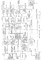
- FIG. 2 is a block diagram of a system with which an interface in accordance with the invention can be utilized.
- FIG. 3 is a block diagram illustrating an interface in accordance with the invention.
- FIG. 4 is a timing diagram depicting by way of illustrative example certain timing signals and the timing of information transferred in accordance with the interface of FIG. 3.
- FIG. 5 is an illustrative example of a format for control information provided to the drive via the interface of FIG. 3.
- FIG. 6 is an illustrative example of a format for status information provided by the drive via the interface of FIG. 3.
- FIG. 7 is an illustrative example of the format of FIG. 6 as utilized to provide particular information.
- FIG. 8 is an illustrative example of the format of FIG. 7 as utilized to provide tape type information.
- FIG. 9 is a flow diagram of an example of a process utilized by the interface of FIG. 3 for reading and transferring data from a computer storage DAT system tape, which is helpful in understanding the operation of the interface of FIG. 3.
- the disclosed invention can be implemented generally in accordance with the ANSI DDS standard referenced in the background, and the following is based upon conformation with ANSI DDS.
- ANSI DDS standard referenced in the background
- other computer data storage recording formats can be utilized to implement the invention.
- DDS formatting organizes data into data groups respectively having 22 or 23 frames, where each frame comprises 2 tracks.
- a Main Area which corresponds to the Main area in DAT audio tapes, stores user data as well as data management information such as the Logical Frame Number (LFN) of the frame with which the particular track is associated.
- LFN Logical Frame Number
- the LFN is the logical position of the frame in the associated data group, which can be different from the actual physical location of the frame due to factors such as rewrites. Further, logical frames can be out of sequence because of appends, rewrites, head clogs during write operations, and bad tape areas.
- DDS formatting supports a read-after-write technique wherein a frame identified as being a bad frame can be re-written downstream of the bad frame, and not necessarily immediately after the bad frame.
- the frame can be re-written after zero, one, two, three, four or five other frames have been written.
- the subject disclosure takes into account such read-after-write procedures without regard to logical frame numbers.
- the tape Subareas store, among other information, the LFN of the associated frame, the Absolute Frame Count (AFC) for the associated frame, a subcode type identifier, a tape area identifier, as well as other information.
- the AFC represents the actual physical location of a frame in the sequence of frames on a tape.
- a data group includes 22 or 23 frames, depending on whether a third level of error correction code (ECC) is utilized with the group, and group boundaries can be indicated by amble frames which have an LFN of 0, by the status of a last frame I.D. bit in the frame header and in the subcode, or by a frame that has an LFN of 1.
- ECC error correction code
- the ATF (automatic track finding) areas contain tracking information utilized for centering the tape heads on the tracks on the tape.
- the system 10 includes a DAT drive 11, a controller 13, and a host computer interface 15, and a host computer.
- the host computer interface can comprise an interface in accordance with the ANSI SCSI standard, or an IBM PC bus compatible interface, for example.
- the drive 11 includes a write audio DAT formatter 111 that receives Main Area information and Subarea information from the controller, appropriately formats such information in accordance with the DAT Conference audio standard, and provides the formatted information to a write amplifier 113 which provides recording signals to the write heads of the drive.
- a local random access memory (RAM) is utilized by the write formatter circuit 111 for storage and processing operations.
- the write formatter circuit 111 assembles the data blocks that are to be recorded in the Main Areas and Subareas of the tape.
- the data blocks for both the Main Areas and the Subareas are organized substantially identically, with each block having a Sync area, an ID area, an ID parity area, and a data area.
- the contents of the Main Area data block data areas is sometimes referred to as Main data, while the contents of the Subarea data block data areas is sometimes referred to as Sub data.
- the information assembled into the data blocks comprises (a) information provided by the controller and (b) information generated or calculated by the formatter.
- the controller provides the following information to the write formatter circuit:
- the write formatter circuit As to the writing of Subarea data blocks, the write formatter circuit generates or calculates the following information:
- the controller provides the following information to the write formatter:
- the write formatter As to writing the Main Area data blocks, the write formatter generates or calculates the following information:
- the drive 11 further includes a read audio DAT formatter circuit 117 which receives tape data from a demodulator 119 that is responsive to the outputs of the read heads of the drive.
- the read formatter circuit decomposes the information read from tape in accordance with the DAT Conference audio standard, so as to provide a Main Area data output to the controller and to store Subarea information in predetermined locations in a local RAM 123 utilized by the read formatter circuit for storage and processing operations.
- a low amplitude detection circuit 121 connected to the demodulator 119 provides a low amplitude signal /LOW-AMP indicative of a playback signal envelope amplitude that is below a predetermined level, which indicative of a bad area on the tape.
- the read formatter circuit disassembles the Main and Sub data blocks read from tape, checks ID parity, checks pack parity, checks C1 ECC parity for the Sub area pack data, checks C1 ECC and C2 ECC parity for the Main data, and transmits the ECC processed Main data to the controller, while making other information read from tape available at predetermined locations in the local RAM 123, for example.
- the write Main data (designated ADDAT) provided by the controller for the Main Area data block data areas is communicated to the write formatter circuit via a unidirectional serial line, while the read Main data (designated DADAT) provided by the read formatter circuit to the controller is communicated via another unidirectional serial line.
- Some error detection information is communicated via dedicated lines, and all other information transferred between the formatter circuits and the controller (designated SPDT data) is communicated via a parallel bus.
- SPDT data includes control information for the formatter circuits, such as sample rate, track pitch, and function (e.g., play, record, high speed). SPDT data also includes read error processing information as accessed by the controller from the read formatter circuit.
- the parallel SPDT data is transferred between the write and read formatter circuits 111, 117 and the controller via a parallel SPDT bus 127 that is common to both formatter circuits.
- Formatter ready signals SPRDY-W and SPRDY-R which indicate that the formatter providing the signal is ready to receive or send data on the parallel SPDT bus 127, are provided by the formatter circuits on respective lines 129, 131.
- Address strobe signals SPAW-W and SPAW-R generated by the controller to transfer address information to the formatter circuits, are provided on respective lines 133, 135 to the formatter circuits 111, 117, respectively.
- Data strobe signals SPSTB-W and SPSTB-R generated by the controller to transfer SPDT data to and from the formatter circuits, are provided on respective lines 137, 139 connected to the formatter circuits 111, 117, respectively.
- the transfer of SPDT data can be pursuant to memory maps for the local RAMs of the formatter circuits, wherein the address locations of the data identify the nature of the data.
- Main data for and from the data areas of the Main Area blocks is transferred between the formatter circuits 111, 117 via respective serial lines 141, 143.
- ADDAT data to be written to tape is serially transferred from the controller to the write formatter circuit 111 on the serial line 141
- DADAT data read from tape is transferred from the read formatter circuit 117 to the controller on the serial line 143.
- the Main Area data transferred to the write formatter circuit for recording can be data as to which error correction parity generation has been performed (e.g., C3 ECC in accordance with the ANSI DDS standard).
- the ADDAT and DADAT data would be logically organized in groups and frames that include appropriate headers in addition to the user data.
- Serial timing signals are provided by the respective formatter circuits via respective timing lines 145, 147 which respectively include a plurality of different timing signals, examples of which will be described in more detail further herein.
- timing signals are synchronized to the rotation of the tape head cylinder, for example by being based on a master signal that controls the rotation of the tape head cylinder, and identify track boundaries, word boundaries, and bit boundaries.
- the formatter circuits 111, 117 generally function as in an audio DAT application.
- the write formatter circuit 111 functions as if it were receiving digital audio data samples from an analog-to-digital converter; and the read formatter circuit 117 functions as if it were providing digital audio data samples to a digital-to-analog converter.
- the ADDAT data to the write formatter emulates the output of an analog-to-digital converter that could be utilized in an audio application
- the DADAT data from the read formatter circuit emulates the input to a digital-to-analog converter that could be utilized in an audio application.
- the read formatter circuit 117 further provides an interpolation flag signal IPF which indicates that C2 ECC parity check of the data read from tape was unable to correct detected errors.
- a formatter synchronizing control 125 synchronizes the operation of the write and read formatter circuits 111, 117 pursuant to a RESET signal provided by the controller. As discussed more fully herein, the synchronizing control 125 synchronizes the operation of the formatter circuits to allow for read-after-write with a 4 head implementation of the drive.
- the drive 11 further includes a drive microprocessor 149 which receives drive commands and provides status information via drive control/status lines 151. Such drive commands control the operation of the drive, and the status information is indicative of the status of the drive.
- the controller 13 includes a microprocessor 211 for controlling the operation of the controller, for assembling the SPDT information transmitted on the parallel bus 127 to the drive, and for processing the SPDT information accessed from the drive on the parallel bus 127.
- a RAM 212 is coupled to the microprocessor 211 via a parallel data bus 213 and a parallel address bus 214, and is utilized by the controller microprocessor 211 for storage and processing operations.
- a bus transceiver 215 coupled to the parallel data bus 213 controls the parallel SPDT bus 127 for transfer of SPDT information.
- An interrupt/wait logic circuit 223 is responsive to the SPRDY signals and provides interrupt and wait signals to the microprocessor 211 for the processing and transfer of data on the parallel SPDT bus 127, as discussed in more detail herein.
- a main area data assembly/control logic circuit 217 which serializes ADDAT data for transfer to the write formatter 111 in the drive 11, and further assembles DADAT data received from the read formatter 117, for example into groups in accordance with the ANSI DDS standard.
- Main Area data and Subarea information as well as Main data block ID information are transferred concurrently, although due to processing requirements the Subarea information being transferred at a given time might not be associated with the Main Area data being transferred at that time.
- the Subarea information and Main data block ID information can be delayed relative to the associated Main Area data by one or two track intervals; and for reading, Main Area data can be delayed relative to the availability of associated Subarea information by one or two track intervals.
- Other read data such as error counts can also be delayed relative to the availability of Subarea information.
- a particular illustrative example of the timing of the interface signals between the drive 11 and the controller 13 will be discussed further herein.
- a status latch 219 is coupled to the data bus 213 and receives the interpolation flag IPF and the low amplitude signal /LOW-AMP from the drive 11.
- a parallel/-serial converter 221 coupled to the data bus 213 is utilized to transfer control/status information between the controller and the drive on the drive control/status lines 151.
- Drive control information is provided by the controller to control the operation of the drive mechanism, while drive status information is provided by the drive as to the status of the drive.
- drive control information is provided by the controller to control the operation of the drive mechanism
- drive status information is provided by the drive as to the status of the drive.
- RXD is used to send commands to the drive. It changes after the high-to-low transition of TRXCLK. Data transfer is MSB first. A command transfer can be initiated by the controller any time /DRDY (discussed below) is asserted.
- TXD is used to receive drive status. It changes after the high-to-low transition to RXCLK. Data transfer is MSB first. RXD and TXD data are sent simultaneously and synchronously.
- TXD and RXD are sampled.
- High 1. Used to transfer I/O.
- the write formatter circuit is in the high impedance state when not enabled by the /SPSTB-W signal (discussed below).
- SPRDY-W is negated when R3CP-W changes, and is asserted beginning a short interval thereafter, for example to allow for processing.
- SPRDY-W can also negated after the end of an /SPSTB-W pulse (discussed below), for example to allow the write formatter to access its local RAM if the write formatter is relatively slower than the controller microprocessor.
- the low-to-high transition causes the I/O address specified by SPDT(7:0) to be written into the write formatter circuit. This address will be used for the next transfer.
- the low-to-high transition causes the data on the SPDT bus to be transferred to/from the write formatter circuit.
- the write formatter can increment the selected I/O address by 1, which would be utilized as the address of the next transfer if no address is specified for such next transfer.
- High 1. Used to transfer I/O.
- the read formatter circuit is in the high impedance state when not enabled by the /SPSTB-R signal (discussed below).
- SPRDY-R is negated when R3CP-R changes, and is asserted a short time thereafter, for example to allow for processing.
- SPRDY-R is also negated after the end of an /SPSTB-R pulse (discussed below), for example to allow the read formatter to access its local RAM if the read formatter is relatively slower than the controller microprocessor.
- the low-to-high transition causes the I/O address specified by SPDT(7:0) to be written into the read formatter circuit. This address will be used for the next /SPSTB-R transfer. After the SPDT data has been transferred, the read formatter can increment the selected I/O address by 1, which would be utilized as the address of the next transfer if no address is specified for such next transfer.
- Data is sent as 16 bit samples synchronized with ADLRCK and /ADBCK.
- the MSB of each sample is sent first.
- ADDAT changes on the high-to-low transition of /ADBCK.
- the Main Area write data bit clock Data on ADDAT is valid on the low-to-high transition of /ADBCK.
- R3CP-W, ADLRCK and ADDAT are changed on the high-to-low transition of /ADBCK.
- /ADBCK runs continuously at 32 times ADLRCK. For a 48 Khz sampling rate, the clock period is 651 nsec.
- Pulses low for one /ADBCK clock period to indicate the boundary between successive 16-bit Main Area write data words. Changes on the low-to-high transition of /ADBCK.
- the Main Area read data bit clock Data on DADAT is valid on the low-to-high transition of /DABCK.
- R3CP-R, DALRCK and DADAT are changed on the high-to-low transition of /DABCK.
- /DABCK runs continuously at 32 times DALRCK. For a 48 Khz sampling rate, the clock period is 651 nsec.
- Pulses low for one /DABCK clock period to indicate the boundary between successive 16-bit Main Area read data words. Changes on the low-to-high transition of /DABCK.
- FIG. 4 shown therein is a timing diagram which sets forth an illustrative example of the pertinent timing signals discussed above and further depicts the processing of data being written to tape and data being read from tape.
- the timing diagram of FIG. 4 also includes other signals and information that can be pertinent to a read-after-write procedure which is advantageously implemented in accordance with the invention. While FIG. 4 depicts the concurrent and phase locked operation of the write and read formatter circuits for providing read-after-write, it should be appreciated that write-only and read-only operations can be implemented.
- the R3CP-W and R3CP-R signals are synchronized with the rotation of the tape head cylinder, and are phase locked to each other with a 180 degree phase difference.
- a complete cycle of an R3CP signal represents one revolution of the tape head cylinder.
- the ADDAT serial data to be recorded and the DADAT serial data from tape are transferred to and from the drive concurrently, with the frame, track, word and bit boundaries being identified by the transitions of the R3CP signals and the other timing signals discussed above.
- Main Area data for a frame is transferred to the drive.
- Main Area data for a frame is transferred to the controller.
- frame boundaries are indicated by MAIN DATA OUT and MAIN DATA IN as coinciding with the positive transitions of the R3CP-W and R3CP-R signals, the phasing of the frame boundaries can be different, depending on implementation and processing requirements. The important consideration is that frame boundaries be defined by intervals that each equal one cycle of the R3CP signals. For example, the frame boundaries of MAIN DATA OUT can lead the positive transitions of R3CP-W by a predetermined number of bit intervals, and the frame boundaries of MAIN DATA IN can lag the positive transitions of R3CP-R by a predetermined number of bit intervals.
- the interpolation flag signal IPF is also provided during the MAIN DATA IN intervals during each word, for example in the middle of the word interval with which the particular IPF signal is associated, as discussed above in the illustrative examples of signal specifications.
- SPDT data including tape Subarea information and Main data block ID information
- the SPDT data can include control information for the formatter circuits, which would require transfer to the formatter circuits.
- SUB DATA in the timing diagram of FIG. 4 is to indicate that Subarea information is to be provided or is available via the SPDT parallel bus during the SUB DATA intervals identified in the timing diagram, with the direction of transfer being indicated by OUT and IN.
- the SUB DATA OUT intervals are defined by the logical AND of the R3CP-W signal and the SPRDY-W signal that is not shown but is essentially the same as the SPRDY-R signal, and the SUB DATA IN intervals are defined by the high states of the SPRDY-R signal.
- the SUB DATA OUT intervals are defined in this manner to provide a single SUB DATA OUT interval for each cycle of the R3CP-W signal, which is appropriate for a tape format in accordance with the ANSI DDS standard that requires that the subareas in both tracks of a frame be identical.
- two SUB DATA OUT intervals can be provided for each R3CP-W cycle if the two tracks of a frame are to include different Subarea information.
- SUB DATA OUT and SUB DATA IN references indicate when Subarea information and any Main Area information communicated via the SPDT bus are transferred from the controller (OUT) and to the controller (IN).
- the direction of transfer of SPDT data on the SPDT parallel bus 127 and the formatter circuit being accessed at any given time are controlled by the microprocessor and the I/O decoder 217.
- the locations in memory maps associated with each of the formatter circuits can be designated as write-only or read-only, and thus the formatter circuit and address being accessed can implicitly define direction.
- the interrupt/wait logic circuit 223 can provide an interrupt pursuant to a SPRDY signal becoming active after a transition of the associated R3CP signal to indicate that data can be transferred on the parallel SPDT bus 127.
- a wait signal can be provided if the formatter circuits are slower than the controller microprocessor 211, for example pursuant to a SPRDY signal becoming inactive prior to the next transition of the associated R3CP signal. Accordingly, although not shown in FIG. 4, the SPRDY signals could have relatively short negative pulses between the negative pulses at the transitions of the associated R3CP signals.
- the interrupt/wait logic circuit would be configured to provide the appropriate interrupt or wait signal, for example, as function of the transitions of the R3CP signals.
- RFOUT identifies the intervals during which one of the write heads is in contact with the tape
- RFIN identifies the intervals during which one of the read heads is in contact with the tape.
- RFOUT intervals start with each transition of the R3CP-W signal and continue for 90 degrees of the R3CP-W cycle, while RFIN intervals start 90 degrees after each transition of the R3CP-R signal.
- FIG. 4 further illustrates the timing sequence for writing and reading of a given frame.
- the Main Area data for the frame N is transferred to the write formatter during the first cycle of the R3CP-W signal associated with the frame N.
- Subarea information and Main data block ID information for the frame N are transferred via the SPDT parallel bus.
- the first track (A) of the frame N is written to tape during first 90 degrees of the third R3CP-W cycle associated with the frame N
- the second track (B) of the frame N is written to tape during the third 90 degrees of the third R3CP-W frame associated with the frame N.
- three cycles of the R3CP-W signal are utilized, with the frame information being processed in pipeline fashion.
- the first track (A) of the written frame N is read from tape during the fourth or last 90 degrees of the third R3CP-W associated with the frame N.
- the second track (B) is read during the second 90 degrees of the fourth cycle of the R3CP-W signal associated with the frame N.
- the first track Subarea information is available a short time after the start of the fourth R3CP-W cycle associated with the frame N, to allow for processing after reading, and the second track Subarea information is available a short time after the 180 degree transition of the fourth R3CP-W cycle associated with the frame N, also to allow for processing.
- a track is read after another adjacent track has been written, in other words by the read head positioned 270 degrees from the write head that wrote such track, in the direction of rotation. In this manner, a recorded track is read in its final form with recorded tracks on either side.
- the Main Area data as read for the frame N is transferred to the controller during the last 180 degrees of the fifth cycle of the R3CP-W signal associated with the frame N and the first 180 degrees of the sixth cycle of the R3CP-W signal associated with the frame N.
- the Subarea information for the first and second tracks are available during the last half of the first R3CP-R cycle associated with the frame, and during the first half of the second R3CP-R cycle associated with the frame.
- Main Area data read for the frame N is available during the third cycle of the R3CP-R signal associated with the frame N. In other words, reading a frame from tape and transferring the frame information to the controller takes place over three cycles of the R3CP-R signal, with the frame information being processed in pipeline fashion.
- FIG. 4 illustrates the availability of certain error data that can be utilized for determining whether re-write is necessary.
- a Main Area ID parity error count IDPCNT, a subcode odd parity error count SOPCNT, a subcode even parity error count SEPCNT, and the LOW AMP signal are available for the first track during the second half of the first R3CP-R cycle, and are available for the second track during the first half of the second R3CP-R cycle.
- the "odd” and “even” terms refer to odd and even numbered blocks.
- the foregoing counts are accessed via the SPDT parallel bus, while the LOW AMP signal is provided on a separate line.
- the C1 ECC processing error count for the Subareas of the first track is available during the first half of the second R3CP-R cycle, while the C1 ECC processing error count for the Subareas of the second track is available during the second half of the second R3CP-R cycle.
- the C1 ECC processing error count for the Main Area of the first track is available for the first track during the second half of the second R3CP-R cycle, while the C1 ECC processing error count for the Main Area of the second track is available during the first half of the third R3CP-R cycle.
- the foregoing C1 error counts are accessed by the controller via the SPDT parallel bus.
- the controller generates a checksum for the Main Area information, which is checked against checksum information in the Subarea information for the frame N during the fourth cycle of R3CP-R.
- such re-write can commence as early as the fifth cycle of the R3CP-W signal associated with the frame (i.e., four frames later), or as late as the seventh cycle of the R3CP-W signal (i.e., six frames later), depending upon the nature of the error detected that calls for a re-write.
- control information transmitted to the drive via the RXD signal discussed above can include two categories, drive modes and drive commands, examples of which are set forth further herein.
- Drive modes generally are directed to drive control operations such as mechanism mode changes that require a relatively longer time to complete, and as to which the controller obtains mode status information to detect that the requested mode is active.
- Drive commands generally are directed to drive operations that can be completed relatively quickly.
- Drive modes and commands can include the following:
- FIG. 5 An illustrative example of the format of an 8-bit control information byte is set forth in FIG. 5, wherein the type of the control information (drive mode or drive command) is identified by bit 6 or 7 being set to 1. If both bits 6 and 7 are set to 0, the control information is a no-operation.
- Status information provided by the drive via the TXD signal discussed above can include information as to status of the drive modes requested by the controller, and also the particular status information requested via drive commands.
- FIG. 6 sets forth an illustrative example of an 8-bit status information byte that can be utilized to communicate status information. If bit 7 is 1 and bit 6 is 0, the drive is currently changing to the drive mode identified in bits (5:0). If bit 7 is 0 and bit 6 is 1, the drive is in the mode identified by bits (5:0). If both bits 7 and 6 are 1, the drive mode or drive command last sent by the controller has been rejected, and bits (5:0) identify the rejected mode or command.
- bit 5 comprises an Eject Requested bit
- bits (4:0) identify a drive status, cassette status, hole status, or error status codes.
- the particular status byte can be presented in response to a command, as a result of an error condition, or as a result of operator actuation of a drive Eject button while the drive is operating pursuant to a "prevent media removal" command.
- a drive status or error code can be returned in response to a drive mode code, with the error code having higher priority. If a drive command is communicated, then the appropriate status code must be returned.
- the cassette status, drive status, and error status information can include the following:
- FIG. 8 sets for a particular example of the format for the code bits of the status byte of FIG. 7.
- Bit 4 is set to indicate that the tape is write-protected; and bit 3 is set to indicate that the tape is pre-recorded.
- Bits (2:0) indicate tape type, which can include the following: TAPE TYPE
- cassette ejection whether or not cassette ejection is permitted can be controlled by the controller, for example to prevent removal of a cassette while recording.
- the drive After the "allow media removal" command has been sent to the drive, the drive will eject the cassette immediately after the Eject button is pushed by an operator. This can also be the default mode after reset. If the controller sends a command after the cassette has been ejected, an error status indicating no cassette will be returned by the drive.
- the drive After the "prevent media removal” command has been sent to the drive, the drive will set the Eject Requested status bit when the Eject button is actuated, and the cassette will not be ejected. This status remains until the controller issues a "cassette eject” command, a "clear Eject Request” command, or an “allow media removal” command, at which time the cassette will be ejected.
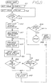
- FIG. 9 set forth therein by way of illustrative example is a flow diagram of a process that can be implemented with the foregoing drive/controller interface for reading a computer storage DAT tape.
- the controller provides a drive mode to the drive via the control/status lines 151 to set the drive mechanism mode to forward at the normal speed of X1.
- the controller requests the drive mode status, and at 313 a determination is made as to whether the requested mode is active. If no, control transfers to 312. This is to allow time for the mode change to be completed.
- a set ATF servo command is provided by the controller at 315.
- the read formatter is set to play, for example, pursuant to formatter control data provided by the controller on the SPDT parallel bus.
- the Subarea and Main Area information read from tape are processed as discussed above.
- the controller periodically requests information as to the drive status, via the control/status lines.
- a determination is made as to whether the drive status provided in response to a request at 321 indicates the end of tape or an error. If no, a determination is made at 325 as to whether reading of the selected information, certain specified groups, for example, has been completed. If no, control transfers to 319 for processing Subarea and Main Area information.
- the controller requests the drive to engage the stop mode at 327.
- the controller requests the drive mode status, and at 329 a determination is made as to whether the requested mode is active. If no, control transfers to 328.
- the stop mode is active, the drive has stopped and the read process is completed.
Landscapes
- Engineering & Computer Science (AREA)
- Theoretical Computer Science (AREA)
- Human Computer Interaction (AREA)
- Physics & Mathematics (AREA)
- General Engineering & Computer Science (AREA)
- General Physics & Mathematics (AREA)
- Signal Processing (AREA)
- Signal Processing For Digital Recording And Reproducing (AREA)
Description
- The disclosed invention is directed generally to computer storage digital audio tape (DAT) drives, and more particularly is directed to an interface between a DAT drive and an associated controller.
- Digital audio tape (DAT) technology, which was developed for audio programming as defined in the DAT Conference Standard, DIGITAL AUDIO TAPE RECORDER, June 1987, published by the Electronic Industries Association of Japan, has been adapted for storage of computer data. An example of a format for the storage of computer data utilizing DAT technology is the American National Standards Institute (ANSI) Digital Data Storage (DDS) standard, presently in draft form ("PROPOSED AMERICAN NATIONAL STANDARD HELICAL-SCAN DIGITAL COMPUTER TAPE CARTRIDGE 381 mm (0.150 in) FOR INFORMATION INTERCHANGE," ASC X3 Project No. 668-D).
- The characteristics that have made DAT technology attractive for computer data storage include high capacity, high transfer rate capability, relatively small media size and low media cost, and the adaptability of DAT technology to conform with personal computer storage device form factors including the 5-1/4 and 3-1/2 inch forms.
- The use of DAT technology for storage of computer data can be achieved by application of a data storage format, such as the above-referenced ANSI DDS standard, to the DAT Conference audio standard. In particular, the DAT audio standard physical track format is retained, but the contents of the information stored in the tracks is in accordance with the computer data storage format.
- DAT technology was developed primarily for audio applications, and therefore an important consideration with the use of DAT technology for computer data storage is the nature of the interface between the DAT drive and the host computer and the requirements of computer data storage.
- EP-
A-0 321 077 is directed to the writing and overwriting of data in a particular data (DAT) format so as to increase the efficiency of overwriting old data, while at the same time, not decreasing the erase/access time or amount of tape necessary to effect such an erasure operation. This reference is not concerned with the function of control of a controller/drive interface as defined in the claims of the subject application. EP-A-0 322 167 describes a general system architecture for accomplishing data transfer to/from a DAT drive. Again this reference is not directed towards providing control information of read/write formatter circuits. EP-A-0 323 890 is directed to the formation, assembly and organization of data in frames, particulary size groups, transferred to and from a tape drive. This reference discloses the use of a Save Set Marks hierarchy that delimits groups of collections of user records on a tape. The Save Set Marks are used for efficient searching of the contents of the tape. - It would therefore be an advantage to provide a computer storage DAT drive controller interface that interfaces with DAT drive having electronic components that were developed for audio applications.
- Another advantage would be to provide a computer storage DAT drive controller interface that provides for full and precise capability of controlling the contents of the information written to tape and precise control of tape operation.
- A further advantage would be to provide a computer storage DAT drive controller interface that interfaces with a DAT drive having electronic components developed for audio applications and which provides for data frame boundary determination in accordance with computer data storage formats.
- According to a first aspect of this invention there is provided a data transfer interface as claimed in
claim 1 herein. - According to a second aspect of this invention there is provided a method for transferring computer data as claimed in claim 10 herein.
- Thus the foregoing and other advantages are provided by the invention in a DAT drive/controller interface for use with a DAT drive having (a) read/write formatting circuitry for writing data to tape in accordance with the DAT Conference format and for reading from tape data recorded in accordance with the DAT Conference format, (b) a tape drive mechanism, and (c) a drive mechanism control circuit. The interface includes transfer and receive circuits for transferring to the read/write formatting circuitry data to be written to tape and for receiving from the read/write circuitry data read from tape, and drive control means for controlling the drive mechanism control circuit.
- The advantages and features of the disclosed invention will readily be appreciated by persons skilled in the art from the following detailed description when read in conjunction with the drawing wherein:
- FIG. 1 is a schematic diagram illustrating the different areas on a single track of a DAT system tape.
- FIG. 2 is a block diagram of a system with which an interface in accordance with the invention can be utilized.
- FIG. 3 is a block diagram illustrating an interface in accordance with the invention.
- FIG. 4 is a timing diagram depicting by way of illustrative example certain timing signals and the timing of information transferred in accordance with the interface of FIG. 3.
- FIG. 5 is an illustrative example of a format for control information provided to the drive via the interface of FIG. 3.
- FIG. 6 is an illustrative example of a format for status information provided by the drive via the interface of FIG. 3.
- FIG. 7 is an illustrative example of the format of FIG. 6 as utilized to provide particular information.
- FIG. 8 is an illustrative example of the format of FIG. 7 as utilized to provide tape type information.
- FIG. 9 is a flow diagram of an example of a process utilized by the interface of FIG. 3 for reading and transferring data from a computer storage DAT system tape, which is helpful in understanding the operation of the interface of FIG. 3.
- In the following detailed description and in the several figures of the drawing, like elements are identified with like reference numerals.
- By way of illustrative example, the disclosed invention can be implemented generally in accordance with the ANSI DDS standard referenced in the background, and the following is based upon conformation with ANSI DDS. However, it should be readily appreciated by persons skilled in the art from a reading of the subject disclosure that other computer data storage recording formats can be utilized to implement the invention.
- For ease of explanation, some aspects of DDS formatting that are pertinent to the invention will be briefly discussed. DDS formatting organizes data into data groups respectively having 22 or 23 frames, where each frame comprises 2 tracks.
- Referring to FIG. 1, set forth therein by way of illustrative example is a schematic layout of one track of a computer data storage DDS DAT tape. A Main Area, which corresponds to the Main area in DAT audio tapes, stores user data as well as data management information such as the Logical Frame Number (LFN) of the frame with which the particular track is associated. The LFN is the logical position of the frame in the associated data group, which can be different from the actual physical location of the frame due to factors such as rewrites. Further, logical frames can be out of sequence because of appends, rewrites, head clogs during write operations, and bad tape areas. DDS formatting supports a read-after-write technique wherein a frame identified as being a bad frame can be re-written downstream of the bad frame, and not necessarily immediately after the bad frame. In particular, the frame can be re-written after zero, one, two, three, four or five other frames have been written. The subject disclosure takes into account such read-after-write procedures without regard to logical frame numbers.
- The tape Subareas store, among other information, the LFN of the associated frame, the Absolute Frame Count (AFC) for the associated frame, a subcode type identifier, a tape area identifier, as well as other information. The AFC represents the actual physical location of a frame in the sequence of frames on a tape.
- A data group includes 22 or 23 frames, depending on whether a third level of error correction code (ECC) is utilized with the group, and group boundaries can be indicated by amble frames which have an LFN of 0, by the status of a last frame I.D. bit in the frame header and in the subcode, or by a frame that has an LFN of 1. However, with read-after-write, the last frames in one group could be meshed with the initial frames in the subsequent group, and the procedure for reading groups will need to recognize and properly process this circumstance.
- The ATF (automatic track finding) areas contain tracking information utilized for centering the tape heads on the tracks on the tape.
- Referring now to FIG. 2, shown therein is a generalized block diagram of a computer storage DAT drive system in which the interface of the invention can be implemented. The system 10 includes a DAT drive 11, a
controller 13, and ahost computer interface 15, and a host computer. The host computer interface can comprise an interface in accordance with the ANSI SCSI standard, or an IBM PC bus compatible interface, for example. - Referring now to FIG. 3, set forth therein are components of the drive 11 and
controller 13 that are pertinent to an interface in accordance with the invention. The drive 11 includes a write audio DAT formatter 111 that receives Main Area information and Subarea information from the controller, appropriately formats such information in accordance with the DAT Conference audio standard, and provides the formatted information to awrite amplifier 113 which provides recording signals to the write heads of the drive. A local random access memory (RAM) is utilized by the write formatter circuit 111 for storage and processing operations. - Generally, the write formatter circuit 111 assembles the data blocks that are to be recorded in the Main Areas and Subareas of the tape. For example, pursuant to the ANSI DDS standard, the data blocks for both the Main Areas and the Subareas are organized substantially identically, with each block having a Sync area, an ID area, an ID parity area, and a data area. The contents of the Main Area data block data areas is sometimes referred to as Main data, while the contents of the Subarea data block data areas is sometimes referred to as Sub data. The information assembled into the data blocks comprises (a) information provided by the controller and (b) information generated or calculated by the formatter.
- As to the writing of Subarea data blocks, the controller provides the following information to the write formatter circuit:
- (a) the W1 byte for the Sub ID area of each Sub data block:
- (b) the
lower order 7 bits of the W2 byte for the Sub ID of each Sub data block; - (c) pack data for the data areas of the Sub data blocks;
- (d) pack parity bytes for the pack data items.
- As to the writing of Subarea data blocks, the write formatter circuit generates or calculates the following information:
- (a) the sync bits for the Sync area of each Sub data block;
- (b) the ID parity byte for the Sub ID parity area of each Sub data block;
- (c) the C1 ECC error correction parity bytes for the Sub data block data areas (in accordance with the DAT Conference audio standard);
- (d) the seventh bit of the W2 byte in the Sub ID area of each Sub data block.
- As to the writing of Main Area data blocks, the controller provides the following information to the write formatter:
- (a) the W1 byte of the Main ID area of each Main data block; and
- (b) data for the data areas of the Main data blocks (e.g., user data).
- As to writing the Main Area data blocks, the write formatter generates or calculates the following information:
- (a) the sync bits for the Sync area of each Main data block;
- (b) the ID parity byte for the Main ID parity area of each Main data block;
- (c) the C1 ECC and C2 ECC error correction parity bytes for the Main data block data areas (in accordance with the DAT Conference audio standard);
- (d) the W2 byte in the Main ID area of each Main data block.
- The drive 11 further includes a read audio DAT formatter circuit 117 which receives tape data from a demodulator 119 that is responsive to the outputs of the read heads of the drive. The read formatter circuit decomposes the information read from tape in accordance with the DAT Conference audio standard, so as to provide a Main Area data output to the controller and to store Subarea information in predetermined locations in a
local RAM 123 utilized by the read formatter circuit for storage and processing operations. - A low
amplitude detection circuit 121 connected to the demodulator 119 provides a low amplitude signal /LOW-AMP indicative of a playback signal envelope amplitude that is below a predetermined level, which indicative of a bad area on the tape. - Generally, the read formatter circuit disassembles the Main and Sub data blocks read from tape, checks ID parity, checks pack parity, checks C1 ECC parity for the Sub area pack data, checks C1 ECC and C2 ECC parity for the Main data, and transmits the ECC processed Main data to the controller, while making other information read from tape available at predetermined locations in the
local RAM 123, for example. - As discussed more fully herein, the write Main data (designated ADDAT) provided by the controller for the Main Area data block data areas is communicated to the write formatter circuit via a unidirectional serial line, while the read Main data (designated DADAT) provided by the read formatter circuit to the controller is communicated via another unidirectional serial line. Some error detection information is communicated via dedicated lines, and all other information transferred between the formatter circuits and the controller (designated SPDT data) is communicated via a parallel bus.
- In addition to tape data block information, SPDT data includes control information for the formatter circuits, such as sample rate, track pitch, and function (e.g., play, record, high speed). SPDT data also includes read error processing information as accessed by the controller from the read formatter circuit.
- The parallel SPDT data is transferred between the write and read formatter circuits 111, 117 and the controller via a
parallel SPDT bus 127 that is common to both formatter circuits. Formatter ready signals SPRDY-W and SPRDY-R, which indicate that the formatter providing the signal is ready to receive or send data on theparallel SPDT bus 127, are provided by the formatter circuits onrespective lines - By way of illustrative example, the transfer of SPDT data can be pursuant to memory maps for the local RAMs of the formatter circuits, wherein the address locations of the data identify the nature of the data.
- Main data for and from the data areas of the Main Area blocks is transferred between the formatter circuits 111, 117 via respective
serial lines 141, 143. In particular, ADDAT data to be written to tape is serially transferred from the controller to the write formatter circuit 111 on theserial line 141, while DADAT data read from tape is transferred from the read formatter circuit 117 to the controller on the serial line 143. Depending upon the tape format specification utilized, the Main Area data transferred to the write formatter circuit for recording can be data as to which error correction parity generation has been performed (e.g., C3 ECC in accordance with the ANSI DDS standard). - For implementation in accordance with the ANSI DDS standard, the ADDAT and DADAT data would be logically organized in groups and frames that include appropriate headers in addition to the user data.
- Serial timing signals are provided by the respective formatter circuits via
respective timing lines - As to the ADDAT and DADAT serial data, the formatter circuits 111, 117 generally function as in an audio DAT application. In particular, the write formatter circuit 111 functions as if it were receiving digital audio data samples from an analog-to-digital converter; and the read formatter circuit 117 functions as if it were providing digital audio data samples to a digital-to-analog converter. Stated another way, the ADDAT data to the write formatter emulates the output of an analog-to-digital converter that could be utilized in an audio application, and the DADAT data from the read formatter circuit emulates the input to a digital-to-analog converter that could be utilized in an audio application.
- The read formatter circuit 117 further provides an interpolation flag signal IPF which indicates that C2 ECC parity check of the data read from tape was unable to correct detected errors.
- A formatter synchronizing control 125 synchronizes the operation of the write and read formatter circuits 111, 117 pursuant to a RESET signal provided by the controller. As discussed more fully herein, the synchronizing control 125 synchronizes the operation of the formatter circuits to allow for read-after-write with a 4 head implementation of the drive.
- The drive 11 further includes a
drive microprocessor 149 which receives drive commands and provides status information via drive control/status lines 151. Such drive commands control the operation of the drive, and the status information is indicative of the status of the drive. - The
controller 13 includes amicroprocessor 211 for controlling the operation of the controller, for assembling the SPDT information transmitted on theparallel bus 127 to the drive, and for processing the SPDT information accessed from the drive on theparallel bus 127. A RAM 212 is coupled to themicroprocessor 211 via aparallel data bus 213 and aparallel address bus 214, and is utilized by thecontroller microprocessor 211 for storage and processing operations. - A
bus transceiver 215 coupled to theparallel data bus 213 controls theparallel SPDT bus 127 for transfer of SPDT information. An interrupt/waitlogic circuit 223 is responsive to the SPRDY signals and provides interrupt and wait signals to themicroprocessor 211 for the processing and transfer of data on theparallel SPDT bus 127, as discussed in more detail herein. - A main area data assembly/
control logic circuit 217 which serializes ADDAT data for transfer to the write formatter 111 in the drive 11, and further assembles DADAT data received from the read formatter 117, for example into groups in accordance with the ANSI DDS standard. - Main Area data and Subarea information as well as Main data block ID information are transferred concurrently, although due to processing requirements the Subarea information being transferred at a given time might not be associated with the Main Area data being transferred at that time. Thus, for example, there can be fixed time relation between (a) the transfer of Main Area data (via DADAT or ADDAT) and (b) the transfer or availability of associated Subarea information and Main data block ID information (via the SPDT bus). By way of illustrative example, for recording, the Subarea information and Main data block ID information can be delayed relative to the associated Main Area data by one or two track intervals; and for reading, Main Area data can be delayed relative to the availability of associated Subarea information by one or two track intervals. Other read data such as error counts can also be delayed relative to the availability of Subarea information. A particular illustrative example of the timing of the interface signals between the drive 11 and the
controller 13 will be discussed further herein. - A status latch 219 is coupled to the
data bus 213 and receives the interpolation flag IPF and the low amplitude signal /LOW-AMP from the drive 11. A parallel/-serial converter 221 coupled to thedata bus 213 is utilized to transfer control/status information between the controller and the drive on the drive control/status lines 151. - Drive control information is provided by the controller to control the operation of the drive mechanism, while drive status information is provided by the drive as to the status of the drive. Particular examples of drive control information, drive status information, and formats, and will be discussed further herein.
- By way of illustrative example, set forth below is a specification of signals in accordance with the invention between the controller and the drive.
- RXD is used to send commands to the drive. It changes after the high-to-low transition of TRXCLK. Data transfer is MSB first. A command transfer can be initiated by the controller any time /DRDY (discussed below) is asserted.
- TXD is used to receive drive status. It changes after the high-to-low transition to RXCLK. Data transfer is MSB first. RXD and TXD data are sent simultaneously and synchronously.
- On or after the low-to-high transition, TXD and RXD are sampled.
- Asserted when the drive is ready to transfer a byte via the TXD and RXD lines. Negates after the byte has been transferred. Asserts again when the drive is ready to accept the next command.
- Asserted by the controller to initialize the drive to its starting state. This is a "hard" reset. It also forces resynchronization of the write and read formatter circuits.
- Two-way tri-state data bus to both write and read formatter circuits. High = 1. Used to transfer I/O. The write formatter circuit is in the high impedance state when not enabled by the /SPSTB-W signal (discussed below).
- Indicates that the transfer of SPDT data to the write formatter circuit possible. In normal write mode, SPRDY-W is negated when R3CP-W changes, and is asserted beginning a short interval thereafter, for example to allow for processing.
- SPRDY-W can also negated after the end of an /SPSTB-W pulse (discussed below), for example to allow the write formatter to access its local RAM if the write formatter is relatively slower than the controller microprocessor.
- The low-to-high transition causes the I/O address specified by SPDT(7:0) to be written into the write formatter circuit. This address will be used for the next transfer.
- The low-to-high transition causes the data on the SPDT bus to be transferred to/from the write formatter circuit. After the SPDT data has been transferred, the write formatter can increment the selected I/O address by 1, which would be utilized as the address of the next transfer if no address is specified for such next transfer.
- Two-way tri-state data bus to both write and read formatter circuits. High = 1. Used to transfer I/O. The read formatter circuit is in the high impedance state when not enabled by the /SPSTB-R signal (discussed below).
- Indicates that the transfer of SPDT data from the read formatter circuit is possible. In normal read mode, SPRDY-R is negated when R3CP-R changes, and is asserted a short time thereafter, for example to allow for processing.
- SPRDY-R is also negated after the end of an /SPSTB-R pulse (discussed below), for example to allow the read formatter to access its local RAM if the read formatter is relatively slower than the controller microprocessor.
- The low-to-high transition causes the I/O address specified by SPDT(7:0) to be written into the read formatter circuit. This address will be used for the next /SPSTB-R transfer. After the SPDT data has been transferred, the read formatter can increment the selected I/O address by 1, which would be utilized as the address of the next transfer if no address is specified for such next transfer.
- 30 Hertz clock which is synchronized to the cylinder rotation. The phase is aligned with track write RF transfers. High = track A (left), low - track B (right). The R3CP-W signal is 180 degrees out of phase with the R3CP-R. R3CP-W changes on the high-to-low transition of /ADBCK (discussed below). R3CP-W is always present, even during STOP, UNLOAD, and EJECT modes.
- A continuous serial bit stream of data to be recorded in the Main Area of each track. Data is sent as 16 bit samples synchronized with ADLRCK and /ADBCK. The MSB of each sample is sent first. ADDAT changes on the high-to-low transition of /ADBCK.
- The Main Area write data word sample clock. High = right channel 16 bit sample, low = left channel 16 bit sample. Changes polarity on high-to-low transitions of every 16th /ADBCK. Goes low when R3CP-W goes high.
- The Main Area write data bit clock. Data on ADDAT is valid on the low-to-high transition of /ADBCK. R3CP-W, ADLRCK and ADDAT are changed on the high-to-low transition of /ADBCK. /ADBCK runs continuously at 32 times ADLRCK. For a 48 Khz sampling rate, the clock period is 651 nsec.
- Pulses low for one /ADBCK clock period to indicate the boundary between successive 16-bit Main Area write data words. Changes on the low-to-high transition of /ADBCK.
- 30 Hertz clock (during play/record) which is aligned with track read RF transfers. High = track A (left), low = track B (right). The R3CP-R signal is 180 degrees out of phase with the R3CP-W signal. R3CP-R changes on the high-to-low transition of /DABCK. R3CP-R is always present, even during STOP, UNLOAD, and EJECT modes.
- A continuous serial bit stream of data from the recorded Main Area of each track. Data is received as 16 bit samples synchronized with DALRCK and DABCK. The MSB of each sample is sent first. R3CP-R changes on the high-to-low transition of /DABCK.
- The Main Area read data sample clock. High = right channel 16 bit sample, low = left channel 16 bit sample. Changes polarity on high-to-low transitions of every 16th /DABCK.
- The Main Area read data bit clock. Data on DADAT is valid on the low-to-high transition of /DABCK. R3CP-R, DALRCK and DADAT are changed on the high-to-low transition of /DABCK. /DABCK runs continuously at 32 times DALRCK. For a 48 Khz sampling rate, the clock period is 651 nsec.
- Pulses low for one /DABCK clock period to indicate the boundary between successive 16-bit Main Area read data words. Changes on the low-to-high transition of /DABCK.
- Indicates that the current 16 bit PCM sample, as defined by DALRCK, contains incorrect data (C2 ECC failure). It is a pulse of nominally 1/2 the length of a DALRCK sample, centered within the associated DALRCK.
- Asserted whenever the playback signal envelope amplitude drops below 50% of the nominal playback envelope amplitude, as determined by a threshold setting.
- Referring now to FIG. 4, shown therein is a timing diagram which sets forth an illustrative example of the pertinent timing signals discussed above and further depicts the processing of data being written to tape and data being read from tape. The timing diagram of FIG. 4 also includes other signals and information that can be pertinent to a read-after-write procedure which is advantageously implemented in accordance with the invention. While FIG. 4 depicts the concurrent and phase locked operation of the write and read formatter circuits for providing read-after-write, it should be appreciated that write-only and read-only operations can be implemented.
- The R3CP-W and R3CP-R signals are synchronized with the rotation of the tape head cylinder, and are phase locked to each other with a 180 degree phase difference. A complete cycle of an R3CP signal represents one revolution of the tape head cylinder.
- The ADDAT serial data to be recorded and the DADAT serial data from tape are transferred to and from the drive concurrently, with the frame, track, word and bit boundaries being identified by the transitions of the R3CP signals and the other timing signals discussed above. In particular, during each of the MAIN DATA OUT intervals that are defined by the positive going transitions of the R3CP-W signal, Main Area data for a frame is transferred to the drive. Similarly, during each of the MAIN DATA OUT intervals defined by the positive going transitions of the R3CP-R signal, Main Area data for a frame is transferred to the controller.
- While the frame boundaries are indicated by MAIN DATA OUT and MAIN DATA IN as coinciding with the positive transitions of the R3CP-W and R3CP-R signals, the phasing of the frame boundaries can be different, depending on implementation and processing requirements. The important consideration is that frame boundaries be defined by intervals that each equal one cycle of the R3CP signals. For example, the frame boundaries of MAIN DATA OUT can lead the positive transitions of R3CP-W by a predetermined number of bit intervals, and the frame boundaries of MAIN DATA IN can lag the positive transitions of R3CP-R by a predetermined number of bit intervals.
- The interpolation flag signal IPF is also provided during the MAIN DATA IN intervals during each word, for example in the middle of the word interval with which the particular IPF signal is associated, as discussed above in the illustrative examples of signal specifications.
- SPDT data, including tape Subarea information and Main data block ID information, can be transferred on the SPDT parallel bus during the intervals identified by SUB DATA OUT and SUB DATA IN, wherein OUT refers to transfers the write formatter circuit 111, and IN refers to transfers between the read formatter circuit 117 and the controller. As discussed above, the SPDT data can include control information for the formatter circuits, which would require transfer to the formatter circuits. The reference to SUB DATA in the timing diagram of FIG. 4 is to indicate that Subarea information is to be provided or is available via the SPDT parallel bus during the SUB DATA intervals identified in the timing diagram, with the direction of transfer being indicated by OUT and IN.
- The SUB DATA OUT intervals are defined by the logical AND of the R3CP-W signal and the SPRDY-W signal that is not shown but is essentially the same as the SPRDY-R signal, and the SUB DATA IN intervals are defined by the high states of the SPRDY-R signal. The SUB DATA OUT intervals are defined in this manner to provide a single SUB DATA OUT interval for each cycle of the R3CP-W signal, which is appropriate for a tape format in accordance with the ANSI DDS standard that requires that the subareas in both tracks of a frame be identical. However, it should appreciated that two SUB DATA OUT intervals can be provided for each R3CP-W cycle if the two tracks of a frame are to include different Subarea information.
- It should be noted that the SUB DATA OUT and SUB DATA IN references indicate when Subarea information and any Main Area information communicated via the SPDT bus are transferred from the controller (OUT) and to the controller (IN).
- The direction of transfer of SPDT data on the SPDT
parallel bus 127 and the formatter circuit being accessed at any given time are controlled by the microprocessor and the I/O decoder 217. By way of illustrative example, the locations in memory maps associated with each of the formatter circuits can be designated as write-only or read-only, and thus the formatter circuit and address being accessed can implicitly define direction. - More particularly as to the function of the SPRDY signals, the interrupt/wait
logic circuit 223 can provide an interrupt pursuant to a SPRDY signal becoming active after a transition of the associated R3CP signal to indicate that data can be transferred on theparallel SPDT bus 127. A wait signal can be provided if the formatter circuits are slower than thecontroller microprocessor 211, for example pursuant to a SPRDY signal becoming inactive prior to the next transition of the associated R3CP signal. Accordingly, although not shown in FIG. 4, the SPRDY signals could have relatively short negative pulses between the negative pulses at the transitions of the associated R3CP signals. The interrupt/wait logic circuit would be configured to provide the appropriate interrupt or wait signal, for example, as function of the transitions of the R3CP signals. - RFOUT identifies the intervals during which one of the write heads is in contact with the tape, and RFIN identifies the intervals during which one of the read heads is in contact with the tape. In terms of relation to the R3CP signals, RFOUT intervals start with each transition of the R3CP-W signal and continue for 90 degrees of the R3CP-W cycle, while RFIN intervals start 90 degrees after each transition of the R3CP-R signal.
- FIG. 4 further illustrates the timing sequence for writing and reading of a given frame. The Main Area data for the frame N is transferred to the write formatter during the first cycle of the R3CP-W signal associated with the frame N. During the second R3CP-W cycle associated with the frame N, Subarea information and Main data block ID information for the frame N are transferred via the SPDT parallel bus. The first track (A) of the frame N is written to tape during first 90 degrees of the third R3CP-W cycle associated with the frame N, and the second track (B) of the frame N is written to tape during the third 90 degrees of the third R3CP-W frame associated with the frame N. Thus, in terms of transferring frame information to the write formatter circuit and writing the frame to tape, three cycles of the R3CP-W signal are utilized, with the frame information being processed in pipeline fashion.
- As to reading, the first track (A) of the written frame N is read from tape during the fourth or last 90 degrees of the third R3CP-W associated with the frame N. The second track (B) is read during the second 90 degrees of the fourth cycle of the R3CP-W signal associated with the frame N. The first track Subarea information is available a short time after the start of the fourth R3CP-W cycle associated with the frame N, to allow for processing after reading, and the second track Subarea information is available a short time after the 180 degree transition of the fourth R3CP-W cycle associated with the frame N, also to allow for processing.
- In the foregoing read-after-write procedure, a track is read after another adjacent track has been written, in other words by the read head positioned 270 degrees from the write head that wrote such track, in the direction of rotation. In this manner, a recorded track is read in its final form with recorded tracks on either side.
- The Main Area data as read for the frame N is transferred to the controller during the last 180 degrees of the fifth cycle of the R3CP-W signal associated with the frame N and the first 180 degrees of the sixth cycle of the R3CP-W signal associated with the frame N.
- In terms of the R3CP-R signal, with the first cycle of the R3CP-R signal associated with the frame N being that cycle during which the first track for the frame N is read from tape as identified by RFIN, the Subarea information for the first and second tracks are available during the last half of the first R3CP-R cycle associated with the frame, and during the first half of the second R3CP-R cycle associated with the frame. Main Area data read for the frame N is available during the third cycle of the R3CP-R signal associated with the frame N. In other words, reading a frame from tape and transferring the frame information to the controller takes place over three cycles of the R3CP-R signal, with the frame information being processed in pipeline fashion.
- Further as to reading the frame N, FIG. 4 illustrates the availability of certain error data that can be utilized for determining whether re-write is necessary.
- A Main Area ID parity error count IDPCNT, a subcode odd parity error count SOPCNT, a subcode even parity error count SEPCNT, and the LOW AMP signal are available for the first track during the second half of the first R3CP-R cycle, and are available for the second track during the first half of the second R3CP-R cycle. The "odd" and "even" terms refer to odd and even numbered blocks. The foregoing counts are accessed via the SPDT parallel bus, while the LOW AMP signal is provided on a separate line.
- The C1 ECC processing error count for the Subareas of the first track is available during the first half of the second R3CP-R cycle, while the C1 ECC processing error count for the Subareas of the second track is available during the second half of the second R3CP-R cycle. The C1 ECC processing error count for the Main Area of the first track is available for the first track during the second half of the second R3CP-R cycle, while the C1 ECC processing error count for the Main Area of the second track is available during the first half of the third R3CP-R cycle. The foregoing C1 error counts are accessed by the controller via the SPDT parallel bus.
- The controller generates a checksum for the Main Area information, which is checked against checksum information in the Subarea information for the frame N during the fourth cycle of R3CP-R.
- In terms of re-write after reading, such re-write can commence as early as the fifth cycle of the R3CP-W signal associated with the frame (i.e., four frames later), or as late as the seventh cycle of the R3CP-W signal (i.e., six frames later), depending upon the nature of the error detected that calls for a re-write.
- Further as to the communication of the drive control and status information on the control/status lines 151, control information transmitted to the drive via the RXD signal discussed above can include two categories, drive modes and drive commands, examples of which are set forth further herein. Drive modes generally are directed to drive control operations such as mechanism mode changes that require a relatively longer time to complete, and as to which the controller obtains mode status information to detect that the requested mode is active. Drive commands generally are directed to drive operations that can be completed relatively quickly.
- Drive modes and commands can include the following:
- DRIVE MODES
- cassette load
- cassette eject
- tape unload, cylinder stop
- cylinder run, tape load
- skip Device Area of tape
- soft stop motion
- hard stop motion
- pause
- forward X1
- forward X3
- forward X5
- forward X7
- forward X11
- forward X12.5
- forward X15
- forward X25
- forward X50
- forward X75
- forward X100
- forward X150
- forward X200
- forward X250
- forward X300
- forward X400
- cylinder stop
- cylinder run
- reverse X1
- reverse X3
- reverse X5
- reverse X7
- reverse X11
- reverse X12.5
- reverse X15
- reverse X25
- reverse X50
- reverse X75
- reverse X100
- reverse X150
- reverse X200
- reverse X250
- reverse X300
- reverse X400
- DRIVE COMMANDS
- get drive mode
- clear eject request bit
- set constant speed servo (record)
- set ATF servo (play)
- cassette status LED off
- cassette status LED on
- drive LED off
- drive LED on
- allow media removal
- prevent media removal
- get hole status
- get cassette status
- get error status
- get drive status
- set 13.6 um track width (read/write)
- set 20.4 um track width (read only)
- drive reset, clear errors
- An illustrative example of the format of an 8-bit control information byte is set forth in FIG. 5, wherein the type of the control information (drive mode or drive command) is identified by
bit bits - Status information provided by the drive via the TXD signal discussed above can include information as to status of the drive modes requested by the controller, and also the particular status information requested via drive commands. FIG. 6 sets forth an illustrative example of an 8-bit status information byte that can be utilized to communicate status information. If
bit 7 is 1 andbit 6 is 0, the drive is currently changing to the drive mode identified in bits (5:0). Ifbit 7 is 0 andbit 6 is 1, the drive is in the mode identified by bits (5:0). If bothbits - If both
bits bit 5 comprises an Eject Requested bit, while bits (4:0) identify a drive status, cassette status, hole status, or error status codes. The particular status byte can be presented in response to a command, as a result of an error condition, or as a result of operator actuation of a drive Eject button while the drive is operating pursuant to a "prevent media removal" command. - In terms of control/status communications for an implementation wherein control information and status information are communicated only simultaneously pursuant to control by the controller (i.e., full duplex communication wherein drive control is slaved to the controller), a drive status or error code can be returned in response to a drive mode code, with the error code having higher priority. If a drive command is communicated, then the appropriate status code must be returned.
- The cassette status, drive status, and error status information can include the following:
- CASSETTE STATUS
- no cassette
- cassette loading
- cassette loaded, length unknown
- cassette loaded, length = 120 min.
- cassette loaded, length = 90 min.
- cassette loaded. length = 60 min.
- cassette loaded, length = 45 min.
- DRIVE STATUS
- no status available
- Beginning of Tape (BOT) leader detect
- End of Tape (EOT) leader detect
- adjust threshold complete
- ERROR STATUS
- no error
- cassette loading error
- cassette eject error
- capstan error
- cylinder error
- reel error or tape jam
- mechanism error
- tape cut
- adjust threshold error
- no cassette
- dew detected, tape, unloaded
- As to tape cassette hole status, FIG. 8 sets for a particular example of the format for the code bits of the status byte of FIG. 7.
Bit 4 is set to indicate that the tape is write-protected; andbit 3 is set to indicate that the tape is pre-recorded. Bits (2:0) indicate tape type, which can include the following:
TAPE TYPE - metal power or equivalent, 13 um thickness
- metal power or equivalent, thin
- wide track, 13 um thickness
- cleaning cassette
- wide track, thin
- As to cassette ejection, whether or not cassette ejection is permitted can be controlled by the controller, for example to prevent removal of a cassette while recording. After the "allow media removal" command has been sent to the drive, the drive will eject the cassette immediately after the Eject button is pushed by an operator. This can also be the default mode after reset. If the controller sends a command after the cassette has been ejected, an error status indicating no cassette will be returned by the drive.
- After the "prevent media removal" command has been sent to the drive, the drive will set the Eject Requested status bit when the Eject button is actuated, and the cassette will not be ejected. This status remains until the controller issues a "cassette eject" command, a "clear Eject Request" command, or an "allow media removal" command, at which time the cassette will be ejected.
- Referring now to FIG. 9, set forth therein by way of illustrative example is a flow diagram of a process that can be implemented with the foregoing drive/controller interface for reading a computer storage DAT tape. At 311 the controller provides a drive mode to the drive via the control/status lines 151 to set the drive mechanism mode to forward at the normal speed of X1. At 312 the controller requests the drive mode status, and at 313 a determination is made as to whether the requested mode is active. If no, control transfers to 312. This is to allow time for the mode change to be completed.
- If the determination at 313 is yes, the requested mode of forward X1 is active, a set ATF servo command is provided by the controller at 315. At 317 the read formatter is set to play, for example, pursuant to formatter control data provided by the controller on the SPDT parallel bus.
- At 319 the Subarea and Main Area information read from tape are processed as discussed above. As the tape is being read, at 321 the controller periodically requests information as to the drive status, via the control/status lines. At 323 a determination is made as to whether the drive status provided in response to a request at 321 indicates the end of tape or an error. If no, a determination is made at 325 as to whether reading of the selected information, certain specified groups, for example, has been completed. If no, control transfers to 319 for processing Subarea and Main Area information.
- If the determination at 323 is yes, or if the determination at 325 is yes, the controller requests the drive to engage the stop mode at 327. At 328 the controller requests the drive mode status, and at 329 a determination is made as to whether the requested mode is active. If no, control transfers to 328. When the stop mode is active, the drive has stopped and the read process is completed.
- Other processes for tape operations will be readily apparent to those skilled in the art.
- The foregoing has been a disclosure of an interface for use with a computer DAT drive that includes components developed for audio DAT applications, and which advantageously provides for recognition of frame boundaries, phase-locked operation of the drive read and write formatter circuits, read-after-write capability, full format capability as to Sub and Main Areas, and precise tape drive mechanism control.
Claims (11)
- A data transfer interface for a digital audio tape DAT system having a write formatter circuit (111) for writing data to tape, a read formatter circuit (117) for reading data from tape, and a drive mechanism control circuit, characterized by:serial data means (141, 143) for transferring to the write formatter circuit (111) main area information to be written to tape, and for receiving from the read formatter circuit (117) main area information read from tape;parallel data means (127) for transferring to the write formatter circuit (111) subarea information to be written to tape, and for receiving from the read formatter circuit (117) subarea information read from tape, said parallel data means further providing control information for controlling the operation of the read and write formatter circuit; anddrive control means for transferring drive control information to the drive control circuit for controlling the operation of the drive.
- The data transfer interface of claim 1 further including host interface means (15) for interfacing the data transfer interface with a host computer.
- The data transfer interface of claims 1 or 2 wherein the data transferred to the write formatter circuit (111) is organised to resemble audio information.
- The data transfer interface of claim 3 wherein the data received from the read formatter circuit (117) resembles audio information.
- The data transfer interface of any preceding claim wherein said parallel data means (127) further accesses error processing information from the read formatter circuit (117).
- The data interface of any one of any preceding claim wherein said serial data means (141, 143) is capable of transmitting and receiving serial data concurrently.
- The controller interface of any preceding claim wherein the main area data received from the drive can comprise a read back version of main area data transferred to the write formatter circuit (111), the read back version being received after a predetermined delay relative to the original main data transfer to the write formatter circuit (111).
- The controller interface of any preceding claim wherein the data written to and read from the tape is in the audio DAT format and wherein said parallel data means (127) transfers to the write formatter circuit (111) further information for the main area data blocks and also transfers to the write and read formatter circuits (111, 117) control information for controlling the operation thereof.
- The controller interface of claim 8 wherein said main area data transferred to the write formatter circuit (111) emulates the output of an audio analog-to-digital converter, and wherein said main area data from the read formatter circuit (117) emulates the input to an audio digital-to-analog converter.
- A method for transferring computer data between a computer storage DAT drive controller and a DAT drive having read and write formatter circuits (117, 111) and a drive mechanism, the method comprising:transmitting to the write formatter circuit (111) for recording in the main areas of the tape a main area serial data stream that emulates the output of an audio analog-to-digital converter;transmitting to the write formatter circuit (111) for recording in the subareas of the tape a parallel data stream of subarea information;receiving from the read formatter circuit (117) a serial data stream read from the main areas of the tape and which is configured to be provided to an audio digital-to-analog converter;receiving from the read formatter circuit (117) a parallel data stream of subarea information read from the subareas of the tape; andproviding control information to the drive to control the mechanical operation thereof.
- The method of claim 10 wherein the step of transmitting a main area serial data stream and the step of receiving a main area serial data stream are coordinated so that the received serial data stream can comprise the read back version of the transmitted main area serial data stream and is delayed relative thereto by a predetermined interval.
Applications Claiming Priority (2)
| Application Number | Priority Date | Filing Date | Title |
|---|---|---|---|
| US46572690A | 1990-01-17 | 1990-01-17 | |
| US465726 | 1990-01-17 |
Publications (3)
| Publication Number | Publication Date |
|---|---|
| EP0437779A2 EP0437779A2 (en) | 1991-07-24 |
| EP0437779A3 EP0437779A3 (en) | 1991-12-18 |
| EP0437779B1 true EP0437779B1 (en) | 1997-06-04 |
Family
ID=23848932
Family Applications (1)
| Application Number | Title | Priority Date | Filing Date |
|---|---|---|---|
| EP90124782A Expired - Lifetime EP0437779B1 (en) | 1990-01-17 | 1990-12-19 | Dat drive/controller interface |
Country Status (3)
| Country | Link |
|---|---|
| EP (1) | EP0437779B1 (en) |
| CA (1) | CA2031343A1 (en) |
| DE (1) | DE69030870T2 (en) |
Families Citing this family (2)
| Publication number | Priority date | Publication date | Assignee | Title |
|---|---|---|---|---|
| DE69229440T2 (en) * | 1992-03-10 | 1999-10-07 | Hewlett Packard Ltd | Data storage device |
| EP0559974A1 (en) * | 1992-03-10 | 1993-09-15 | Hewlett-Packard Limited | Data storage apparatus |
Family Cites Families (4)
| Publication number | Priority date | Publication date | Assignee | Title |
|---|---|---|---|---|
| US4652944A (en) * | 1984-06-25 | 1987-03-24 | Kirsch Technologies, Inc. | Computer memory back-up |
| EP0321077B1 (en) * | 1987-12-14 | 1994-03-02 | Sony Corporation | Apparatus and method for recording a digital signal |
| CA1270324A (en) * | 1987-12-22 | 1990-06-12 | Garry Hutchinson | Dat storage system for computers |
| GB8800353D0 (en) * | 1988-01-08 | 1988-02-10 | Hewlett Packard Ltd | Data storage method |
-
1990
- 1990-12-03 CA CA002031343A patent/CA2031343A1/en not_active Abandoned
- 1990-12-19 EP EP90124782A patent/EP0437779B1/en not_active Expired - Lifetime
- 1990-12-19 DE DE69030870T patent/DE69030870T2/en not_active Expired - Fee Related
Also Published As
| Publication number | Publication date |
|---|---|
| DE69030870T2 (en) | 1997-12-18 |
| CA2031343A1 (en) | 1991-07-18 |
| EP0437779A2 (en) | 1991-07-24 |
| DE69030870D1 (en) | 1997-07-10 |
| EP0437779A3 (en) | 1991-12-18 |
Similar Documents
| Publication | Publication Date | Title |
|---|---|---|
| JP2854391B2 (en) | Method for assembling data groups on DAT tape | |
| JP2576512B2 (en) | Data recorder | |
| EP0272130A2 (en) | Data recording | |
| US6182191B1 (en) | Recording and reproducing system | |
| US5539914A (en) | Method and system for preprocessing data block headers during access of data in a data storage system | |
| JP4032433B2 (en) | Tape cassette and tape recording apparatus | |
| US5796690A (en) | Disc controller with improved data sync and re-sync mark detection | |
| US8274749B1 (en) | Data wedge format table synchronization | |
| US5535327A (en) | Method and apparatus for communicating formatted data from a mass storage device to a host computer | |
| EP0096456B1 (en) | Capstanless magnetic tape drive with electronic equivalent to length of tape | |
| EP0437779B1 (en) | Dat drive/controller interface | |
| JPH0727687B2 (en) | Data recorder | |
| CA2031336A1 (en) | Dat drive/controller interface | |
| US6735156B2 (en) | Recording method for rewritable optical disk | |
| JP2595096B2 (en) | Control method of magnetic tape unit and buffer memory | |
| JP2522272B2 (en) | Data recorder | |
| JPH04503126A (en) | read-write head buffer | |
| JP2576509B2 (en) | Data recorder | |
| JP2576497B2 (en) | Data recorder | |
| JP2625734B2 (en) | Data recorder | |
| JPH04286755A (en) | Magnetic recording/regenerating device | |
| JPS63173274A (en) | Data recording system | |
| JPH0828056B2 (en) | Data recorder | |
| JPS6381663A (en) | Data checking system for magnetic disk | |
| JPH07307063A (en) | Data recording method |
Legal Events
| Date | Code | Title | Description |
|---|---|---|---|
| PUAI | Public reference made under article 153(3) epc to a published international application that has entered the european phase |
Free format text: ORIGINAL CODE: 0009012 |
|
| AK | Designated contracting states |
Kind code of ref document: A2 Designated state(s): DE FR GB IT SE |
|
| PUAL | Search report despatched |
Free format text: ORIGINAL CODE: 0009013 |
|
| AK | Designated contracting states |
Kind code of ref document: A3 Designated state(s): DE FR GB IT SE |
|
| 17P | Request for examination filed |
Effective date: 19920224 |
|
| 17Q | First examination report despatched |
Effective date: 19941201 |
|
| RAP1 | Party data changed (applicant data changed or rights of an application transferred) |
Owner name: CONNER PERIPHERALS, INC. |
|
| GRAG | Despatch of communication of intention to grant |
Free format text: ORIGINAL CODE: EPIDOS AGRA |
|
| GRAH | Despatch of communication of intention to grant a patent |
Free format text: ORIGINAL CODE: EPIDOS IGRA |
|
| GRAH | Despatch of communication of intention to grant a patent |
Free format text: ORIGINAL CODE: EPIDOS IGRA |
|
| GRAA | (expected) grant |
Free format text: ORIGINAL CODE: 0009210 |
|
| AK | Designated contracting states |
Kind code of ref document: B1 Designated state(s): DE FR GB IT SE |
|
| PG25 | Lapsed in a contracting state [announced via postgrant information from national office to epo] |
Ref country code: IT Free format text: LAPSE BECAUSE OF FAILURE TO SUBMIT A TRANSLATION OF THE DESCRIPTION OR TO PAY THE FEE WITHIN THE PRE;WARNING: LAPSES OF ITALIAN PATENTS WITH EFFECTIVE DATE BEFORE 2007 MAY HAVE OCCURRED AT ANY TIME BEFORE 2007. THE CORRECT EFFECTIVE DATE MAY BE DIFFERENT FROM THE ONE RECORDED.SCRIBED TIME-LIMIT Effective date: 19970604 Ref country code: FR Effective date: 19970604 |
|
| REF | Corresponds to: |
Ref document number: 69030870 Country of ref document: DE Date of ref document: 19970710 |
|
| PG25 | Lapsed in a contracting state [announced via postgrant information from national office to epo] |
Ref country code: SE Effective date: 19970904 |
|
| EN | Fr: translation not filed | ||
| REG | Reference to a national code |
Ref country code: GB Ref legal event code: 732E |
|
| PLBE | No opposition filed within time limit |
Free format text: ORIGINAL CODE: 0009261 |
|
| STAA | Information on the status of an ep patent application or granted ep patent |
Free format text: STATUS: NO OPPOSITION FILED WITHIN TIME LIMIT |
|
| 26N | No opposition filed | ||
| REG | Reference to a national code |
Ref country code: GB Ref legal event code: 732E |
|
| PGFP | Annual fee paid to national office [announced via postgrant information from national office to epo] |
Ref country code: DE Payment date: 20001124 Year of fee payment: 11 |
|
| PGFP | Annual fee paid to national office [announced via postgrant information from national office to epo] |
Ref country code: GB Payment date: 20001127 Year of fee payment: 11 |
|
| PG25 | Lapsed in a contracting state [announced via postgrant information from national office to epo] |
Ref country code: GB Free format text: LAPSE BECAUSE OF NON-PAYMENT OF DUE FEES Effective date: 20011219 |
|
| REG | Reference to a national code |
Ref country code: GB Ref legal event code: IF02 |
|
| PG25 | Lapsed in a contracting state [announced via postgrant information from national office to epo] |
Ref country code: DE Free format text: LAPSE BECAUSE OF NON-PAYMENT OF DUE FEES Effective date: 20020702 |
|
| GBPC | Gb: european patent ceased through non-payment of renewal fee |
Effective date: 20011219 |