EP0436293A2 - Inverse multiplexer and demultiplexer techniques - Google Patents
Inverse multiplexer and demultiplexer techniques Download PDFInfo
- Publication number
- EP0436293A2 EP0436293A2 EP90312744A EP90312744A EP0436293A2 EP 0436293 A2 EP0436293 A2 EP 0436293A2 EP 90312744 A EP90312744 A EP 90312744A EP 90312744 A EP90312744 A EP 90312744A EP 0436293 A2 EP0436293 A2 EP 0436293A2
- Authority
- EP
- European Patent Office
- Prior art keywords
- subsectional
- data rate
- rate
- domain frame
- time domain
- Prior art date
- Legal status (The legal status is an assumption and is not a legal conclusion. Google has not performed a legal analysis and makes no representation as to the accuracy of the status listed.)
- Granted
Links
- 238000000034 method Methods 0.000 title claims abstract description 42
- 239000003550 marker Substances 0.000 claims abstract description 22
- 230000005540 biological transmission Effects 0.000 claims description 15
- 238000011084 recovery Methods 0.000 claims 2
- 230000001419 dependent effect Effects 0.000 claims 1
- 230000001360 synchronised effect Effects 0.000 abstract description 6
- 230000000737 periodic effect Effects 0.000 abstract 1
- 230000015654 memory Effects 0.000 description 13
- 238000004891 communication Methods 0.000 description 9
- RGNPBRKPHBKNKX-UHFFFAOYSA-N hexaflumuron Chemical compound C1=C(Cl)C(OC(F)(F)C(F)F)=C(Cl)C=C1NC(=O)NC(=O)C1=C(F)C=CC=C1F RGNPBRKPHBKNKX-UHFFFAOYSA-N 0.000 description 6
- 238000006243 chemical reaction Methods 0.000 description 4
- 238000010586 diagram Methods 0.000 description 4
- 238000013507 mapping Methods 0.000 description 4
- 230000006978 adaptation Effects 0.000 description 3
- 230000006870 function Effects 0.000 description 3
- 230000008569 process Effects 0.000 description 3
- 238000004364 calculation method Methods 0.000 description 2
- 239000002131 composite material Substances 0.000 description 2
- 238000013461 design Methods 0.000 description 2
- 238000003780 insertion Methods 0.000 description 2
- 230000037431 insertion Effects 0.000 description 2
- 101150067286 STS1 gene Proteins 0.000 description 1
- 101100028967 Saccharomyces cerevisiae (strain ATCC 204508 / S288c) PDR5 gene Proteins 0.000 description 1
- 101150027289 Ubash3b gene Proteins 0.000 description 1
- 102100040338 Ubiquitin-associated and SH3 domain-containing protein B Human genes 0.000 description 1
- 230000008901 benefit Effects 0.000 description 1
- 230000002457 bidirectional effect Effects 0.000 description 1
- 238000010276 construction Methods 0.000 description 1
- 238000011161 development Methods 0.000 description 1
- 238000012986 modification Methods 0.000 description 1
- 230000004048 modification Effects 0.000 description 1
- 239000013307 optical fiber Substances 0.000 description 1
- 230000004044 response Effects 0.000 description 1
Images


Classifications
-
- H—ELECTRICITY
- H04—ELECTRIC COMMUNICATION TECHNIQUE
- H04L—TRANSMISSION OF DIGITAL INFORMATION, e.g. TELEGRAPHIC COMMUNICATION
- H04L25/00—Baseband systems
- H04L25/02—Details ; arrangements for supplying electrical power along data transmission lines
- H04L25/14—Channel dividing arrangements, i.e. in which a single bit stream is divided between several baseband channels and reassembled at the receiver
-
- H—ELECTRICITY
- H04—ELECTRIC COMMUNICATION TECHNIQUE
- H04J—MULTIPLEX COMMUNICATION
- H04J2203/00—Aspects of optical multiplex systems other than those covered by H04J14/05 and H04J14/07
- H04J2203/0001—Provisions for broadband connections in integrated services digital network using frames of the Optical Transport Network [OTN] or using synchronous transfer mode [STM], e.g. SONET, SDH
- H04J2203/0089—Multiplexing, e.g. coding, scrambling, SONET
- H04J2203/0094—Virtual Concatenation
Abstract
Description
- The present invention relates to inverse multiplexer techniques that demultiplex high non-standard channel data rate signals and adapt each non-standard data rate signal to lower standard channel data signals for transmission over a commercial communication network to a remote receiver where an inverse demultiplexer adapts and multiplexes the received standard data rate signals to reproduce the original non-standard higher data rate signal and transmit it to the destined user.
- In recent years there is a substantial need for communicating with data rates between 10 Mb/s to 1 Gb/s, as, for example, the SONET STS1 51.84 Mb/s and SONET STS3 155.52 Mb/s transmission rates, High Definition Television programming at 120 Mb/s or greater, and a Gb/sec supercomputer transmission rate. Such applications cannot directly transmit data messages over existing telecommunications networks using, for example, the 45 Mb/s DS3 rate, because the data rate of the specialized application does not match, and may be greater than the data rate used by the existing telecommunication networks. Therefore, to transmit data messages for such applications between remote locations, it becomes necessary to build a separate, specially designed, telecommunication network to link these remote locations. Where such remote locations are spread over wide distances, such as across the United States, the development costs may not justify construction of short or long haul facilities to support each of the different specialized applications.
- An alternative solution might be to design specialized data rate converters to meet the criteria of each application. In this regard see, for example, U. S. Patent 4,322,844 issued to F. Fellinger et al. on March 30,1982, where a transmitter-receiver synchronizer provides bidirectional rate conversion between frames of data having a first rate and a first format, and frames of data having a second rate and a second format. In such synchronizer, a first frame of data at a first rate, and a second frame of data at a second rate are stored in a separate first and second buffer memory, respectively, during a first frame interval, and each frame of data is read out at the other rate during a second frame interval. Additionally, during the second frame interval, a third frame of data at the second rate, and a fourth frame of data at the first rate are read into the first and second buffer memories, respectively, and read out at the other rate during a third frame interval, etc. Another synchronizer is shown in U. S. patent 4,558,445 issued to L. R. Novick on December 10,1985, wherein an applique rate converter generates a composite data stream comprising alternate data bits and data boundary bits, and the synchronizer increases such composite stream to the output data rate. Such specialized arrangements are expensive and would require a new design for converting different data rates associated with each different application, and may not be usable for all applications.
- Therefore, the problem remaining in the prior art is to provide a technique that permits specialized applications to economically send their higher data rate signal over existing lower data rate telecommunication networks, and thereby avoid constructing expensive specialized high data rate long or short haul networks, or expensive specialized data rate converters, and provide for a more economic use of the unused capacity of existing networks.
- The foregoing problem in the prior art has been solved in accordance with the present invention which relates to Inverse Multiplexer and Inverse Demultiplexer techniques. An Inverse Multiplexer includes a Demultiplexer which demultiplexes a high data rate input signal to subsectional output signals which comprise fractional parts of that high data rate signal, and synchronization means which marks each of the subsectional output signals for later resynchronization at the receiver. A Programmable Multiplexer then multiplexes one or more of such subsectional output rate signals for transmission over existing facilities.
- Other and further aspects of the present invention will become apparent during the course of the following description and by reference to the accompanying drawings.
-
- FIG. 1 is a block diagram of an exemplary arrangement of a communication system for practicing the present invention;
- FIG. 2 is an illustration of the preferred rate-adaptation technique which maps a capacity domain frame into a time domain frame for an exemplary input signal to a Programmable Multiplexer in the arrangement of FIG. 1 using a two-step method in accordance with the present invention;
- FIG. 3 is a table listing the conversion of the capacity domain to time domain assignments for use in the mapping of FIG. 2 for the exemplary two-step method in accordance with the present invention;
- FIG. 4 is a block diagram of an exemplary programmable multiplexer in accordance with the present invention; and
- FIG. 5 is a block diagram of an alternative programmable multiplexer in accordance with the present invention.
- FIGS. 6 and 7 are block diagrams of a preferred embodiment of the synchronization and resynchronization means of FIG. 1.
- FIG. 1 illustrates an exemplary arrangement for each of an
Inverse Multiplexer 10 and a remote Inverse Demultiplexer 20 which are interconnected to form an exemplary communication system in accordance with the present invention. For purposes of explanation only, and not for purposes of limitation, the following description of the present invention will be directed to (1) an exemplaryInverse Multiplexer 10 which receives an exemplary SONET ST3 155.52 Mb/s transmission rate input signal, and transmits such input signal over fourexemplary DS3 45 Mb/srate channels 15₁ to 15₄ of a conventional communication system to (2) an exemplary remote Inverse Demultiplexer 20 for receiving the exemplary four DS3 channel signals and reconstructing the exemplary original SONET ST3 signal therefrom. It is to be understood that the input signal can comprise any data rate other than the SONET ST3 signal which is greater than the data rate of thecommunication channels 15 used by the communication system for transmission between remote locations. - In FIG 1. the exemplary
Inverse Multiplexer 10 is shown as comprising aDemultiplexer 11, a synchronization means 12, and a plurality of N=4 Rate Adaptation means which can comprise any suitable means, but hereinafter will be described in relationship to Programmable Multiplexers (PMUXs) 13₁ to 13₄. In operation, Demultiplexer 11 receives the exemplary SONET ST3 155.52 Mb/s data rate input signal, and demultiplexes the input signal into a plurality of subsectional output signals, where each subsectional output signal includes a data rate which is less than the exemplary standard 45 Mb/sDS3 channel 15 transmission data rate. Such demultiplexing should produce subsectional output signals with data rates that (1) are fractional parts of the input data rate, and (2) are less than the data rate of thecommunication system channels 15. It is to be understood that each subsectional output signal should have a data rate less than thecommunication system channel 15 data rate, but need not have a data rate which equals the data rate of any of the other subsectional output signals. For purposes of explanation only, however, it will be assumed thatdemultiplexer 11 produces four subsectional output signals having equal data rates of 38.88 Mb/s each, which is less than the 45 Mb/sexemplary DS3 channel 15 transmission data rate. - It is to be understood that
demultiplexer 11 could have produced any number of subsectional output signals above 4 with equal or unequal data rates, as long as each of the subsectional output signals had a data rate which is less than thechannel 15 transmission data rate of the communication system being used. For the above example, at least 4 subsectional output signals are required for the present exemplary 155.52 Mb/s rate input signal, since any lesser number would produce at least one subsectional output signal with a data rate higher than the exemplary 45 Mb/schannel 15 data rate. Each of thesedemultiplexer 11 subsectional output signals are transmitted overseparate paths 14, or other means, e.g., channels, to a synchronizing means 12. - Synchronizing means 12 can comprise a separate synchronizer for each subsectional output signal from
demultiplexer 11, as shown in FIG. 6 for a preferred embodiment of synchronizing means 12. In FIG. 6, an exemplary arrangement for asynchronizer 12₄, in the transmitting end, is shown as comprising anelastic store 40, amarker insert circuit 41 and a phase lock loop comprising alow pass filter 42 and a Voltage Control Oscillator (VCO) 43. In operation, a clock at the input data rate (e.g., 155.52 Mb/s) is received inInverse multiplexer 10 and divided by N (e.g., N=4) to produce the subsectional clock signal at the data rate of the input subsectional output signal (e.g., 38.88 Mb/s) fromdemultiplexer 11. The subsectional clock signal is provided to each of thesynchronizers 12₁, to 12₄, but, for purposes of simplicity, only one of the synchronizers is shown as receiving this clock signal, which for the present example of FIG. 6 issynchronizer 12₄. In thesynchronizer 12ielastic store 40 receives the subsectional output data and clock signals and places gaps in the data stream to permit markers to be inserted at predetermined intervals. Markerinsert 41 receives both the data from theelastic store 40 and the clock signal from the output of the phase lock loop comprisinglow pass filter 42 andVCO 43, and periodically inserts a marker signal into the subsectional output data stream fromelastic store 40. Markerinsert 41 also provides a clock signal, associated with the clock from the phase lock loop, toelastic store 40, and a synchronizing pulse externally to each of theother synchronizers 12₁ to 12₃, ifsynchronizer 12₄ is the master synchronizer. Each of theother synchronizers 12₁ to 12₃ use such synchronization pulse frommarker insert 41 ofsynchronizer 12₄ along with the input clock signal provided byphase lock loop synchronizer 12₄. The data and clock signals frommarker insert 41 are then sent to the associated PMUX 13i. Therefore, each synchronizer inserts a synchronization marker into each subsectional output signal fromDMUX 11 in response to a synchronization pulse, and passes the synchronized subsectional output signal to the associated PMUX 13i. For purposes of explanation hereinafter, it will be assumed that the 38.88 Mb/s subsectional output signal fromDMUX 11 was increased to 39.00 Mb/s at the output of eachsynchronizer 12 by the inclusion of the associated marker signal in eachsynchronizer 12i. - Each of the four synchronized data rate subsectional output signals from synchronizing
means 12 is provided to the input of a separate one ofPMUXs 13₁ to 13₄. Since each of the PMUX of the exemplary arrangement of FIG. 1 are shown as receiving a single input signal at a data rate of 39 Mb/s at Data Port A and no signal at Data Port B, the following description ofPMUX 13₁ also applies to each ofPMUXs 13₂ to 13₄. It should be understood, however, that any Inverse Multiplexer should include two functions; tributary synchronization and rate adaptation. Tributary synchronization is required to automatically compensate for difference in the DS3 path lengths ofchannels 15 due to differences in circuit packs, cross-connect cables, and wires or optical fibers. The problem can be solved by inserting synchronized digital markers into each of the paths orchannels 15 at the transmit end and then using that marker information to realign the frames at the receiving end. The delay required by the realignment process can be provided by large elastic stores. - The second function of rate adaptation will always be required since the input data rate will almost never be a convenient multiple of the exemplary DS3 channel rate. A solution is to insert data from another source into fixed positions within the exemplary DS3 frame to stuff the incoming data up to the exemplary DS3 rate. Such synchronization process is described in copending patent application Serial No. 459,929 filed for R. R. McKnight et al. on the same day as the present application, and assigned to the same assignee. The arrangement of FIG. 1 only shows a single active input at Data Port A to each of PMUXs 13, but the insertion of data from another source at Data Port B, etc., is shown in above-mentioned copending patent application to R. R. McKnight et al. Such arrangement will be described briefly once the operation of
PMUX 13₁ with a single input has been described. - PMUX 13₁ receives the exemplary synchronized 39 Mb/s subsectional input signal and inserts such signal up into the 45 Mb/s DS3 frame so that the signal is substantially evenly distributed over the DS3 frame by mapping the input requirements in the capacity domain into a time domain. As described in detail in the above-mentioned copending patent application to R. R. Mcknight et al., a PMUX can accomplish this via a 2-step or 3-step digit reversal technique. For purposes of explanation only, the following description is directed to the 2-step digit reversal technique. The fundamental goal of the digit reversal technique is to provide a mapping from a capacity domain to a time domain.
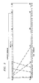
- FIG. 2 illustrates an example of the mapping of the capacity domain to the time domain for the 2-step digit reversal technique for a
PMUX 13₁ comprising only the 39 Mb/s subsectional output signal at input data port A. For purposes of description, it will be assumed that the capacity domain includes a capacity frame 30 of forty-five sequential capacity domain time slots (CTSs 00-44) with each Capacity domain Time Slot representing and exemplary 1 Mb/s of capacity. For the present example, data port A receives a subsectional output signal with a 39 Mb/s data rate from synchronization means 12. Since only an integral number of Capacity Time Slots (CTS) can be assigned to a data port, data port A will be assigned 39 CTSs in a contiguous segment of the capacity domain frame. An optional asynchronouspulse stuffing algorithm 72 of FIG. 4 can be used to fill in any fraction of a CTS which is not needed for the subsectional output signal. As shown in FIG. 2 for the capacity domain frame 30, data port A is arbitrarily assigned CTSs 00-38 to accommodate the 39.00 Mb/s capacity requirement. It is to be understood that data ports A could have been assigned any portion of the 00-44 CTSs of the capacity domain frame 30 which does not overlap other data port (e.g., Data Port B) requirements. - In accordance with a first step of the present digit reversal technique, the capacity domain CTS address is decomposed as a predetermined number of digits (e.g., 3 digits for the 00-44 CTS) from a set of number bases. More particularly, to determine the number bases to be used, any combination of numbers that, when multiplied together, will provide the number of CTSs of the capacity domain frame 30 can be used. For example, for the 45 CTSs of the capacity domain frame 30, combinations such a 9 and 5; 3 and 15; and 3, 3, and 5 when multiplied together will yield a value of 45. Although any of these combinations may be used for the following calculations, the following example will use the number bases 3,3 and 5 since it provides a clearer example of the method. Typically, using a combination with more numbers, e.g. 3, 3 and 5 rather than just 5 and 9, will provide a somewhat more even distribution of the CTSs amongst the Time Domain Time Slots (TDTS) in
Time Capacity frame 31. However, factors of 3 are best combined with other factors rather than separate, to obtain uniformity of distribution. Therefore, for the number systems of 3, 3, and 5 to be used, the available range of numbers would be 0-2, 0-2 and 0-4, respectively, as is well known in the art. In decomposing the capacity domain CTS numbers for the exemplary number systems chosen, the first step of the present digit reverse technique uses the equation:

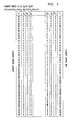
where X is the CTS address, and X₁ to X₃ are integers which would be substituted to produce the CTS address X. - FIG. 3 shows a Table which illustrates the various values of X₁ to X₃ which need to be multiplied with the associated data base numbers in Equation (1) to produce each of the CTS addresses. For example, for the CTS address where X=00 in capacity domain frame 30 of FIG.2, representative of the first CTS of data port A, X₁ to X₃ would have to equal zero in equation (1) to yield X=00. Similarly, for CTS address X=38 in frame 30 of FIG. 2, representative of the last CTS for data port A, X₁ would have to equal 2, X₂ would have to equal 1, and X₃ would have to equal 3 in equation (1) to yield 30+5+3=38.
- Having completed the above first step for each of the used CTSs in capacity domain frame 30, the second step is to generate a digit reverse technique by reversing (1) the number base sequence, and (2) the Xi values, and generate the following equation in the same manner as used for generating equation (1):

where Y is the assigned representative time slot in a exemplary DS3Time Domain frame 31, comprising 45 time slots, for the CTS of Capacity Domain frame 30 of FIG. 2. For example, for CTS 05 of Capacity Domain 30 assigned to data port A, in accordance with the Table of FIG. 2, X₁ and X₃ of equation (1) would equal 0 while X₂ would equal 1 to produce X=05. Substituting these Xi values into equation (2) would produce Y=03 representative of time slot 03 oftime domain frame 31. Therefore, the data in CTS 05 in frame 30 would be transmitted overchannel 15₁ of FIG. 1 as data in time slot 03 ofTime Domain frame 31 using this 2-step digit reverse technique. Similarly, as seen from the Table of FIG. 2, the data assigned toCTSs 08 and 23 would be transmitted overchannel 15₁ intime slots 30 and 31, respectively, oftime domain frame 31. In this manner the contiguously assigned capacity domain time slots in frame 30 for data port A are distributed somewhat uniformly throughtime domain frame 31, as are the unused CTSs for CTSs 39-44, which are stuffed. - An alternative 3-step digit reverse technique can be used to provide a more even distribution of the CTSs of capacity domain frame 30 In this 3-step digit reverse technique the first step of the above-described 2-step technique using equation (1) is repeated as the first step of the 3-step digit reverse technique. A second step of the 3-step digit reverse technique involves the conversion of the determined values of X₁ to X₃ into equivalent Y₁ to Y₃ values, respectively, using modular arithmetic as described in the copending patent application to R.R. Mcknight et at. The third step of the 3-step digit reverse technique uses the equation

which is derived in the same manner as equation (2) but substitutes the Yi for the Xi values of equation (2). It is to be understood that the advantage of the present 2-step and 3-step techniques are that the time slots are substantially uniformly distributed within a time domain frame and that all capacity domain CTSs are guaranteed to be mapped insidetime domain frame 31. - Exemplary arrangements for
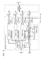
programmable multiplexer 13₁ for performing the above 2-step or 3-step techniques are shown in FIGs. 4 and 5. In FIG. 4 aframe counter 60 receives a clock signal which is passed through a plurality of dividing circuits 61-63 that provide binary value outputs relating to the time slot numbers in time domain frames 31 in FIG. 2. For purposes of explanation, the following description of the PMUX of FIG. 4 will be related to the prior example of a capacity and time domain frame of 45 CTSs, where the number bases 3, 3 and 5 are used. Therefore,frame counter 60 would include a divide-by-3circuit 61, a divide-by-3circuit 62, and a divide-by-5circuit 63. Since the binary output from the divide-by-3circuits circuit 63 provides 3 output leads to take care of the possible 000, 001, 010, 011 and 100 binary codes. The first output lead from divide-by-3circuit 61 will be considered as the Least Significant Bit (LSB) while the highest value binary output lead from divide-by-5circuit 63 is considered the Most Significant Bit (MSB). It should be noted that the LSB-MSB bits fromframe counter 60 are coupled tocomparators circuit 61 to the MSB input forcomparator 67 of Data Port A, to automatically produce the digit reversal technique. - Each input data port terminated as an input to a PMUX 13, is provided with a
Start Bit Memory 65 and anEnd Bit Memory 66 which are coupled to a first associatedComparator 67 and a second associatedComparator 68, respectively. These memories and Comparators are effectively associated with the Capacity Domain frame 30 of FIG. 2. Each of first and second Comparators receives the bits on the 7 output leads fromframe counter 60 in the reverse order at separate inputs thereof. The outputs from each of the first andsecond Comparators gate 69, and the output from ANDgate 69 is connected to a first input of a separate second ANDgate 70. The data signal from asynchronizer 12i associated with that input Data Port is applied to the second input of the associated ANDgate 70. The outputs from the second ANDgate 70 is shown as coupled to an input of an optional ORgate 71, with the output ofOR gate 71 being applied to channel 15₁ for transmission to the far-end Inverse Demultiplexer 20. - In operation, a control signal initializes the
Start Bit memory 65 andEnd Bit memory 66 for each of the input data ports, which for the present example is only Data Port A. In the present example shown in FIG. 2, the start and end bitmemories End Bit memories PMUX 13₁ would be set at 39 and 40-44, respectively, depending on the amount of capacity domain required, but could not be more than the unassigned 6 CTSs. - In the present example, when
frame counter 60 provides binary signals on its 7 output leads indicating the address of a particular Time Domain Time slot, each offirst comparators 67 compares the associated stored Start Bit value with the bit reverse binary value fromframe counter 60 and outputs a binary "1" if the reversed binary value fromframe counter 60 is equal to or greater than the associated Start Bit value, and a "0" if the reversed binary value fromframe counter 60 is less than the stored Start Bit. Similarly, each ofsecond comparators 68 compares the associated stored End Bit value with the reversed binary values fromframe counter 60 and outputs a binary "1" if the associated End Bit value is equal to or less than the received reversed binary value fromframe counter 60, and a binary "0" if the associated End Bit value is greater than the reversed binary value received fromframe counter 60. - Therefore, for the period of time of time domain time slot number Y=12,
frame counter 60 would output the equivalent binary value for 1,1,0 for X₃ to X₁, respectively, as shown in the table of FIG. 3. Each ofcomparators frame counter 60, because of the lead reversal betweenframe counter 60.Comparators 67 then compare the stored Start Bit value of associatedmemory 65 with the received reverse binary code.Only comparator 67 for Data Port A would output a binary "1" since this comparator would find it equal to or greater than the stored Start Bit value of 00 in associatedStart Bit memory 65.Comparators 67 for any other Data Port would determine that the received reverse binary code is less than the stored Start Bit value and output a binary "0". However, forcomparators 68 of Data Port A, and Data Port B, eachcomparator 68 would output a binary "1" since the receivedbinary code End Bit memories 66. - As a result, only AND
gate 69 associated with Data Port A would produce a binary "1" enable output signal during time domain frame time slot Y=12 because both of its inputs fromcomparators gate 69 of Data Port A provides a binary "1" enable signal to ANDgate 70 to permit the input data signal from Data Port A to pass therethrough, and to optional ORgate 71, for transmission overchannel 15₁. A similar process occurs for each of the time domain time slots Y=00-38 in the Table of FIG. 3 to permit Data Port A to be accessed in accordance with the capacity domain during each of the Time Domain Time Slots. If Data Port B were included, then the associatedcomparators gates - To permit the 3-step technique to be performed, an
optional converter 73 need only be disposed at the output offrame counter 60 to perform the conversion for the number base values from X₁ to X₃ to Y₁ to Y₃, respectively, using modular arithmetic as described in copending patent Application to R. R. McKnight et at. These converted Y₁ to Y₃ values are then used in equation (2) for X₁ to X₃, respectively. FIG. 5 illustrates an exemplary alternative preferred arrangement for performing the 2-step or 3-step digit reverse technique, in which the capacity domain parameters are provided to aprocessor 80, such as a personal or other computer or microprocessor, andprocessor 80 performs the appropriate 2-step or 3-step capacity domain to time domain calculations. The results are then stored in aRAM 81 and used in a table look-up manner to provide port selection to multiplex the input Data Port A (and B) signals ontochannels 15₁ to 15₄ in the manner shown in FIGs. 2 and 3. - At the receiving end,
Inverse Demultiplexer 20 of FIG. 1 includes a plurality of Programmable Demultiplexers (PDMUXs), which for the exemplary four channel system are designated 23₁ to 23₄. The output fromPDMUXs 23₁ to 23₄ are the recovered exemplary 39.00 Mb/s data rate signals that were provided as inputs toPMUXs 13₁ to 13₄, respectively atInverse Multiplexer 10. The output signals fromPDMUXs 23₁ to 23₄ are provided as inputs to a resynchronizing means 24. ThePDMUXs 23₁ to 23₄, and resynchronizing means 24, at the receiving end operate in the reverse manner from thePMUXs 13₁ to 13₄ and synchronizing means 12 at the transmitting end, to recover the original exemplary demultiplexed 38.88 Mb/s input data signals. AMultiplexer 25 then multiplexes the four exemplary 38.88 Mb/s output signals from desynchronizing means 24 to produce the original exemplary SONET ST3 155.52 Mb/s input signal and transmit it to an end user device. - At the receiving end, in
Inverse Demultiplexer 20, the resynchronizer means 24 can comprise separate resynchronizers 24₁ to 24₄, for each ofPMUXs 23₁ to 23₄, respectively. As shown in FIG. 7, the data and clock subsectional signals from each ofPMUX 23₁ to 23₄ is received in resynchronizers 24₁ to 24₄, respectively. The Random Access Memory (RAM) 46 is used as a large elastic store to compensate for differences in propagation delay intransmission channels 15₁ to 15₄. For purposes of explanation, the following discussion is directed to the operation of resynchronizer 24₄, and it should be understood that each of resynchronizers 24₁ to 24₃ operate in a similar manner. The data subsectional signal fromPMUX 23₄ is received in a marker detect 44 which detects the marker inserted bymarker insert 41 ofsynchronizer 12₄ in thedistant Inverse Multiplexer 10, and sends both the marker detect output signal as a reset signal to awrite counter 45 forming part of aRAM 46, and the received data stream to aHigh Speed RAM 47 via itscontrol circuit 48. The clock subsectional signal is also received inwrite counter 45, and is used to increment the address signal to the RAM for writing the data stream from marker detect 44 into sequential addressed memory locations withinRAM 47. A read counter 49 functions toaddresses RAM 47 to read out the stored data at a subsectional output rate equal to the exemplary 38.88 Mb/s data rate, excluding the markers inserted bymarker insert 41 ofInverse Multiplexer 10, and deliver such data stream to MUX 25. InMux 25, the data from resynchronizers 24₁ to 24₄ are multiplexed to generate the SONET 155.52 Mb/s output signal. Read counter obtains the clock signals for reading the data fromRAM 47 from a phase locked loop comprising aPhase Detector 50, which compares the read and write counter phases to generate a control signal for Voltage Control Oscillator 51, which is corrected to produce an output signal which equals the 155.52 Mb/s rate. The Divide-By-N circuit 52 generates the 38.88 Mb/s clock signal forread counter 49. Read counter 49 in resynchronizer 24₄ also generates a synchronization pulse at the same time it resets itself, with the repetition period equal to the marker insertion interval used bymarker insert 41 generated insynchronizer 12₄ ofInverse Multiplexer 10. This synchronization pulse from read counter 49 in resynchronizer 24₄ is distributed to resynchronizers 24₁ to 24₃ to reset their associated read counters 49. Because each write counter 45 in resynchronizer 24₁ to 24₄ is reset by the synchronization marker associated with its respective subsectional data signal, the data written intoRAMs 47 of each of resynchronizers 24₁ to 24₄ is resynchronized with respect to the RAM addresses obtained from write counters 45 in the associated resynchronizer. Because the read counters 49 in each of resynchronizers 24₁ to 24₃ are synchronized to read counter 49 in resynchronizer 24₄, the data is read out of theRAMs 47 of resynchronizers 24₁ to 24₄ and presented to themultiplexer 25 in resynchronized order. - It is to be understood that other modifications can be made to the arrangements described hereinbefore and still fall within the spirit and scope of the present invention. For example, it is possible to perform asynchronous pulse stuffing in each of
PMUX 13₁ to 13₄ by including additional input ports beyond input A, and optional inputs B, which provide stuffing indicator bits. Then, any additional unused capacity domain time slots (CTSs) can be used to increase the contiguous CTSs for an input Data Port, and the additional PMUX 13 input ports can be used to indicate the stuff bits at the appropriate time domain time slots. Furthermore, the original exemplary 155.52 Mb/s input signal to DMUX 11 could have been demultiplexed into other than four 38.88 Mb/s subsectional output signals, as, for example, eight 19.44 Mb/s subsectional output signals. For such example, it is possible for each of the 19.44 Mb/s signals to be stuffed to, for example, a 20 Mb/ssynchronizer 12 output signal, and a separate two of the eight 20 Mb/s subsectional output signals provided to the A and B data ports ofPMUXs 13₁ to 13₄, since the combination of two 20 Mb/s signals is less than the 45 Mb/s DS3 rate.
Claims (7)
- A method of transmitting a first data rate input signal to a remote terminal over transmission channels including a lower second data rate, the method comprising the steps of:(a) demultiplexing the first data rate input signal into a plurality of subsectional output signals, each subsectional output signal comprising a data rate which is lower than the second data rate;(b) inserting a marker signal at a predetermined timing relationship into each of the plurality of subsectional output signals at predetermined internals;(c) receiving at separate inputs of each of one or more rate adaptor means, subsectional output signals from step (b) that in combination for each rate adaptor means does not total more than the capacity of the second data rate, and inserting those subsectional output signals into a separate output signal a the second data rate; and(d) transmitting two or more second data rate signals from step (c) over two or more second data rate transmission channels to a remote one or more receivers for recovery of the first data input signal;
wherein in performing step (c) performing the substeps of:(c1) assigning each subsectional output signal associated with a rate adaptor means to one or more predetermined contiguous addresses of a capacity domain frame dependent on the data rate of the received subsectional output signal, where the capacity domain frame includes a predetermined number of assignable addresses;(c2) in each rate adaptor means, converting each of the contiguous addresses of the capacity domain frame for each of the received subsectional output signals from step (b) to non-contiguous addresses in a time domain frame so that the non-contiguous addresses are substantially uniformly distributed over the time domain frame; and in performing step (d) transmitting sections of one of the subsectional output signals during each address of the time domain frame sequence, as determined in step (c), via one of the second data rate transmission channnels to a remote one or more receivers for recovery of the first data rate input signal. - The method according to claim 1, wherein in performing step (c2), performing the substeps of(e) in each rate adaptor means, counting through a time domain frame in a predetermined sequence from a first to a last address of a counting sequence, the counting sequence being represented by a multibit word including N individual segments;(f) generating N binary words, each word containing one or more bits, each word being associated with one of the N segments of step (e);(g) comparing the multibit word from step (f) in a reverse order with a first and a second number defining a start and stop address, respectively, associated with predetermined contiguous addresses in the capacity domain assigned in step (c1) to each of the subsectional output signals, for assigning which one of the one or more subsectional output signals will be assigned to each address of the time domain frame.
- The method according to claim2, wherein
in performing step (f), performing the substeps of(f1) converting the predetermined number of addresses in the capacity domain frame into a plurality of separate number bases which when multiplied together yield said predetermined number of addresses in the capacity domain frame; and(f2) translating each of the addresses of the capacity domain frame into a separate binary word for each of the number bases determined in step (f1). - The method according to claim 3 wherein
in performing step (g), using the number bases in reverse order from that of step (f1) and the binary output values from step (f2) in a reverse order for assigning each time domain frame address to a particular one of the one or more subsectional output signals. - The method according to claim 1 wherein the method comprises the further step of:(e) concurrently performing steps (b) to (d) at each of the two or more rate adaptor means, and each rate adaptor means performing step (d) by transmitting sections of the associated subsectional output signals over a separate one of the second data rate channels.
- The method according to claim 5 wherein the method comprises the further steps of:
at the remote receiver,(f) receiving a time domain frame sequence, transmitted in step (d) by each of the one or more first rate adaptor means, at a separate second rate adaptor means for recovering each subsectional output signal forming said time domain frame sequence at a separate output of each second rate adaptor means;(g) removing the marker signal from each of the recovered subsectional output signals forming each time domain frame; and(h) multiplexing each of the subsectional output signals from each of the second rate adaptor means into an output signal corresponding to the first data rate input signal. - The method according to claim 1 wherein the method comprises the further steps of:
at the remote receiver,(e) receiving the time domain frame sequence, transmitted in step (d) by each of the one or more first rate adaptor means, at a separate second rate adaptor means for recovering each subsectional output signal forming said time domain frame sequence at a separate output of the second rate adaptor means;(f) removing the marker signal from each of the recovered subsectional output signals forming each time domain frame; and(g) multiplexing each of the subsectional output signals of step (f) from each of the second rate adaptor means into an output signal corresponding to the first data rate input signal.
Applications Claiming Priority (2)
| Application Number | Priority Date | Filing Date | Title |
|---|---|---|---|
| US460209 | 1990-01-02 | ||
| US07/460,209 US5065396A (en) | 1990-01-02 | 1990-01-02 | Inverse multiplexer and demultiplexer techniques |
Publications (3)
| Publication Number | Publication Date |
|---|---|
| EP0436293A2 true EP0436293A2 (en) | 1991-07-10 |
| EP0436293A3 EP0436293A3 (en) | 1991-10-30 |
| EP0436293B1 EP0436293B1 (en) | 1995-02-01 |
Family
ID=23827780
Family Applications (1)
| Application Number | Title | Priority Date | Filing Date |
|---|---|---|---|
| EP90312744A Expired - Lifetime EP0436293B1 (en) | 1990-01-02 | 1990-11-22 | Inverse multiplexer and demultiplexer techniques |
Country Status (6)
| Country | Link |
|---|---|
| US (1) | US5065396A (en) |
| EP (1) | EP0436293B1 (en) |
| JP (1) | JPH0761055B2 (en) |
| AU (1) | AU618694B2 (en) |
| CA (1) | CA2031054C (en) |
| DE (1) | DE69016634T2 (en) |
Cited By (18)
| Publication number | Priority date | Publication date | Assignee | Title |
|---|---|---|---|---|
| EP0461445A2 (en) * | 1990-06-09 | 1991-12-18 | CONTROLWARE GmbH KOMMUNIKATIONSSYSTEME | Method for transmitting at a high data rate over a plurality of lower speed channels |
| EP0533091A2 (en) * | 1991-09-12 | 1993-03-24 | Fujitsu Limited | Parallel transmission method |
| EP0565890A2 (en) * | 1992-04-16 | 1993-10-20 | Siemens Aktiengesellschaft | Method and system for the transmission of a data signal in a VC-12-container in transmission channels |
| EP0612174A2 (en) * | 1993-02-19 | 1994-08-24 | AT&T Corp. | A wide area network (WAN) arrangement |
| EP0675620A1 (en) * | 1994-03-30 | 1995-10-04 | Nec Corporation | Parallel data transmission unit using byte error correcting code |
| WO1997047155A1 (en) * | 1996-05-30 | 1997-12-11 | Siemens Aktiengesellschaft | Method for transmitting data between a sending station and a receiving station assigned to it |
| FR2771878A1 (en) * | 1997-12-03 | 1999-06-04 | Telecommunications Sa | Connection procedure for linking two local area networks |
| EP0996246A2 (en) * | 1998-10-16 | 2000-04-26 | Marconi Communications Limited | Communication system |
| EP1024632A2 (en) * | 1999-01-27 | 2000-08-02 | CSELT Centro Studi e Laboratori Telecomunicazioni S.p.A. | A method of and a device for digital signal transmission using inverse multiplexing |
| WO2000048419A2 (en) * | 1999-02-11 | 2000-08-17 | Siemens Aktiengesellschaft | Method for the administration of pcm channels for multi-channel connections, whereby said pcm channels belong together |
| EP1045612A1 (en) * | 1999-04-12 | 2000-10-18 | International Business Machines Corporation | Method and system for re-synchronizing channels supporting the inverse multiplexing function |
| EP1045610A2 (en) * | 1999-04-12 | 2000-10-18 | International Business Machines Corporation | Method for resynchronizing a group of B channels in an ISDN network |
| EP1098462A2 (en) * | 1999-11-03 | 2001-05-09 | ECI Telecom Ltd. | Method and system for increasing bandwith capacity utilisation |
| WO2001056237A1 (en) * | 2000-01-27 | 2001-08-02 | Siemens Aktiengesellschaft | Method and device for equalising transmission running times during the transmission of data through several transmission channels |
| EP1183608A1 (en) * | 1999-03-30 | 2002-03-06 | McData Corporation | Interconnection architecture for managing multiple low bandwidth connections over a high bandwidth link |
| AT410739B (en) * | 2000-05-26 | 2003-07-25 | Ericsson Ahead Comm Systems Gm | SYSTEM AND METHOD FOR TRANSMITTING DATA |
| US6618176B2 (en) | 1995-05-11 | 2003-09-09 | Ciena Corporation | Remodulating channel selectors for WDM optical communication systems |
| GB2472203A (en) * | 2009-07-28 | 2011-02-02 | Europ Satellites Ltd | Providing hotel room entertainment services over plural twisted wire pairs |
Families Citing this family (94)
| Publication number | Priority date | Publication date | Assignee | Title |
|---|---|---|---|---|
| US5062105A (en) * | 1990-01-02 | 1991-10-29 | At&T Bell Laboratories | Programmable multiplexing techniques for mapping a capacity domain into a time domain within a frame |
| US5351239A (en) * | 1990-03-16 | 1994-09-27 | Newbridge Networks Corporation | Digital data transmission system |
| US5257261A (en) * | 1990-07-27 | 1993-10-26 | Transwitch Corporation | Methods and apparatus for concatenating a plurality of lower level SONET signals into higher level sonet signals |
| US5331641A (en) * | 1990-07-27 | 1994-07-19 | Transwitch Corp. | Methods and apparatus for retiming and realignment of STS-1 signals into STS-3 type signal |
| EP0555267A4 (en) * | 1990-09-24 | 1994-05-18 | Transwitch Corp | Sonet signal generating apparatus and method |
| US5491695A (en) * | 1991-07-17 | 1996-02-13 | Digital Access Corporation | Means and method of dial up bridging of network for high bandwidth digital communication |
| US5231649A (en) * | 1991-08-08 | 1993-07-27 | Ascend Communications, Inc. | Method and apparatus for dynamic bandwidth allocation in a digital communication session |
| JPH0575651A (en) * | 1991-09-13 | 1993-03-26 | Nec Corp | Packet transmission system |
| US5251210A (en) * | 1991-11-01 | 1993-10-05 | Ibm Corporation | Method and apparatus for transforming low bandwidth telecommunications channels into a high bandwidth telecommunication channel |
| US5550825A (en) * | 1991-11-19 | 1996-08-27 | Scientific-Atlanta, Inc. | Headend processing for a digital transmission system |
| WO1993013609A1 (en) * | 1991-12-23 | 1993-07-08 | Network Express | System for internetworking data terminal equipment through a switched digital network |
| US5341369A (en) * | 1992-02-11 | 1994-08-23 | Vitesse Semiconductor Corp. | Multichannel self-routing packet switching network architecture |
| FI90297C (en) * | 1992-04-02 | 1994-01-10 | Nokia Telecommunications Oy | Network interface procedure and network interface for a digital data network |
| JP2682334B2 (en) * | 1992-05-29 | 1997-11-26 | 日本電気株式会社 | Image signal coding transmission method |
| CA2140533C (en) * | 1992-07-20 | 2004-11-23 | Roland Bruckner | Method for forwarding a message cell stream via a plurality of parallel trunks while adhering to the sequence of the message cells |
| US5610945A (en) * | 1993-11-04 | 1997-03-11 | International Business Machines Corporation | System for identifying communication sequences transmitted across multiple carriers by examining bit streams for sequences of valid words |
| US6125398A (en) * | 1993-11-24 | 2000-09-26 | Intel Corporation | Communications subsystem for computer-based conferencing system using both ISDN B channels for transmission |
| JPH07154447A (en) * | 1993-11-29 | 1995-06-16 | Nec Corp | High-speed data transmission circuit |
| US5579239A (en) * | 1994-02-16 | 1996-11-26 | Freeman; Mitchael C. | Remote video transmission system |
| US5390239A (en) * | 1994-03-17 | 1995-02-14 | Morris; Gregory A. | Method for increasing digital data throughput over telephone lines |
| US5617417A (en) * | 1994-09-07 | 1997-04-01 | Stratacom, Inc. | Asynchronous transfer mode communication in inverse multiplexing over multiple communication links |
| US6972786B1 (en) | 1994-12-30 | 2005-12-06 | Collaboration Properties, Inc. | Multimedia services using central office |
| US5751338A (en) * | 1994-12-30 | 1998-05-12 | Visionary Corporate Technologies | Methods and systems for multimedia communications via public telephone networks |
| US5581566A (en) * | 1995-01-06 | 1996-12-03 | The Regents Of The Univ. Of California Office Of Technology Transfer | High-performance parallel interface to synchronous optical network gateway |
| FI100212B (en) * | 1995-03-06 | 1997-10-15 | Nokia Telecommunications Oy | High speed data transmission in mobile networks |
| US9191117B2 (en) * | 1995-05-11 | 2015-11-17 | Ciena Corporation | High-speed optical transponder systems |
| US5570356A (en) * | 1995-06-07 | 1996-10-29 | International Business Machines Corporation | High bandwidth communications system having multiple serial links |
| US5598413A (en) * | 1995-07-10 | 1997-01-28 | Adtran, Inc. | Four-wire, half-rate architecture with embedded differential delay compensation for extending range of basic rate ISDN communications |
| US5974031A (en) * | 1995-10-25 | 1999-10-26 | Hewlett-Packard Company | Automatic detection of a telecommunications fractional channel configuration |
| US5627820A (en) * | 1995-10-25 | 1997-05-06 | Hewlett-Packard Company | Automatic detection of a telecommunications fractional channel |
| US5923667A (en) * | 1996-06-28 | 1999-07-13 | International Business Machines Corporation | System and method for creating N-times bandwidth from N separate physical lines |
| KR0171029B1 (en) * | 1996-06-28 | 1999-03-30 | 정선종 | Pulse shaping filter for ñ/4 transfer qpsk modulator |
| US5781598A (en) * | 1996-08-14 | 1998-07-14 | Hardy, Iii; Harmon S. | System and method of asynchronous data transfer through a plurality of modems |
| US5987030A (en) | 1996-09-27 | 1999-11-16 | Cisco Technology, Inc. | Transparent circuit emulation for packet switching network |
| US6215798B1 (en) * | 1996-11-01 | 2001-04-10 | Telefonaktiebolaget Lm Ericsson (Publ) | Multi-frame synchronization for parallel channel transmissions |
| US5850398A (en) * | 1996-12-30 | 1998-12-15 | Hyundai Electronics America | Method of scheduling data cell transmission in an ATM network |
| US6002692A (en) * | 1996-12-30 | 1999-12-14 | Hyundai Electronics America | Line interface unit for adapting broad bandwidth network to lower bandwidth network fabric |
| US5949788A (en) * | 1997-05-06 | 1999-09-07 | 3Com Corporation | Method and apparatus for multipoint trunking |
| US6330248B1 (en) * | 1997-12-05 | 2001-12-11 | Advanced Micro Devices, Inc. | Arrangement for transmitting data packets from a media access controller across multiple physical links |
| US6134246A (en) * | 1998-01-26 | 2000-10-17 | Samsung Electronics Co., Ltd. | Inverse multiplexing within asynchronous transfer mode communication networks |
| US6693904B1 (en) * | 1998-04-09 | 2004-02-17 | Lucent Technologies Inc. | Trace format for a sliced switch fabric |
| US6266345B1 (en) * | 1998-04-24 | 2001-07-24 | Xuan Zhon Ni | Method and apparatus for dynamic allocation of bandwidth to data with varying bit rates |
| US6618374B1 (en) * | 1998-09-10 | 2003-09-09 | Cisco Technology, Inc. | Method for inverse multiplexing of ATM using sample prepends |
| US6917630B1 (en) * | 1998-10-06 | 2005-07-12 | Nortel Networks Limited | Concatenation of containers in synchronous digital hierarchy network |
| EP1119984A4 (en) * | 1998-10-15 | 2001-12-19 | Airnet Communications Corp | Method for dynamic allocation of wireless base station dsp resources |
| US6370579B1 (en) * | 1998-10-21 | 2002-04-09 | Genuity Inc. | Method and apparatus for striping packets over parallel communication links |
| GB9828367D0 (en) * | 1998-12-22 | 1999-02-17 | Northern Telecom Ltd | Method and apparatus for communicating information |
| US6873630B1 (en) * | 1999-05-19 | 2005-03-29 | Sun Microsystems, Inc. | Method and apparatus for a multi-gigabit ethernet architecture |
| US6956852B1 (en) * | 1999-06-25 | 2005-10-18 | Cisco Technology Inc. | Multi-function high-speed network interface |
| US6792003B1 (en) * | 1999-08-12 | 2004-09-14 | Nortel Networks Limited | Method and apparatus for transporting and aligning data across multiple serial data streams |
| US6625161B1 (en) | 1999-12-14 | 2003-09-23 | Fujitsu Limited | Adaptive inverse multiplexing method and system |
| US7260099B1 (en) * | 2000-07-14 | 2007-08-21 | Nortel Networks Limited | Processing of arbitrarily formatted client signals to achieve compatibility with existing transport networks |
| US7716358B2 (en) | 2000-09-12 | 2010-05-11 | Wag Acquisition, Llc | Streaming media buffering system |
| US6766376B2 (en) | 2000-09-12 | 2004-07-20 | Sn Acquisition, L.L.C | Streaming media buffering system |
| US8595372B2 (en) * | 2000-09-12 | 2013-11-26 | Wag Acquisition, Llc | Streaming media buffering system |
| DE10057933B4 (en) * | 2000-11-22 | 2020-02-06 | Smsc Europe Gmbh | Method for transmitting an anisochronous data stream on an isochronous transmission path |
| US7006509B1 (en) | 2000-12-22 | 2006-02-28 | Cisco Technology, Inc. | Method and system for graceful slowlink deletion and subsequent fast link addition in an IMA group |
| US6952434B1 (en) | 2000-12-27 | 2005-10-04 | Cisco Technology, Inc. | System and method for processing control cells to prevent event missequencing and data loss in IMA groups |
| US7065104B1 (en) | 2000-12-28 | 2006-06-20 | Cisco Technology, Inc. | Method and system for managing inverse multiplexing over ATM |
| US7237035B1 (en) | 2001-02-12 | 2007-06-26 | Ceterus Networks, Inc. | Frame structure and method for wavelength concatenated channel framing |
| US6738540B2 (en) * | 2001-06-22 | 2004-05-18 | Lucent Technologies Inc. | Optical cross-connect switch using programmable multiplexers/demultiplexers |
| US7155127B2 (en) * | 2001-08-15 | 2006-12-26 | Nippon Telegraph And Telephone Corporation | Optical communication system, optical communication unit, and optical transceiving package |
| US7286570B2 (en) * | 2001-11-21 | 2007-10-23 | Alcatel-Lucent Canada Inc | High speed sequenced multi-channel bus |
| US7623541B2 (en) * | 2001-11-23 | 2009-11-24 | Smsc Europe Gmbh | Apparatus for transmitting an anisochronic data stream on an isochronic transmission route |
| AU2002347459A1 (en) | 2001-11-26 | 2003-06-10 | Nokia Corporation | Mac layer inverse multiplexing in a third generation ran |
| US20030229844A1 (en) * | 2002-03-25 | 2003-12-11 | Akash Bansal | Graceful degradation of serial channels |
| ES2325483T3 (en) * | 2002-04-09 | 2009-09-07 | Abb Schweiz Ag | REDUNDANT TRANSMISSION OF PROTECTION ORDERS BETWEEN TELERUPTORS. |
| US7362777B2 (en) * | 2002-06-27 | 2008-04-22 | Nortel Networks Limited | Concatenated transmission of synchronous data |
| US7586950B1 (en) | 2002-09-13 | 2009-09-08 | Ceterus Networks, Inc. | Remote management interface |
| US7570671B2 (en) * | 2002-11-20 | 2009-08-04 | Infinera Corporation | Method and apparatus for deploying forward error correction in optical transmission networks and the deployment of photonic integrated circuit (PIC) chips with the same |
| US7505486B2 (en) * | 2002-11-19 | 2009-03-17 | Hewlett-Packard Development Company, L.P. | Degradable network data path transmission scheme |
| JP4007313B2 (en) * | 2003-01-22 | 2007-11-14 | 株式会社村田製作所 | Angle sensor |
| US20040196798A1 (en) * | 2003-04-01 | 2004-10-07 | Abousleman Glen P | System and method for wireless transmission of signals using multiple channels assigned in response to signal type |
| US7882510B2 (en) * | 2003-08-06 | 2011-02-01 | Microsoft Corporation | Demultiplexer application programming interface |
| US7308561B2 (en) * | 2003-12-12 | 2007-12-11 | Alcatel Lucent | Fast, scalable pattern-matching engine |
| US7209998B2 (en) * | 2004-02-04 | 2007-04-24 | Qualcomm Incorporated | Scalable bus structure |
| KR20070011315A (en) * | 2004-02-19 | 2007-01-24 | 조지아 테크 리서치 코오포레이션 | Systems and methods for parallel communication |
| US7349444B2 (en) * | 2004-08-23 | 2008-03-25 | Transwitch Corporation | SONET/SDH SPE/virtual container retiming with adaptive dual pointer leak rate computation |
| JP4464238B2 (en) * | 2004-09-30 | 2010-05-19 | 富士通株式会社 | Wireless relay device, wireless relay method, information communication system |
| US20100142947A1 (en) * | 2008-12-08 | 2010-06-10 | Jong-Yoon Shin | Apparatus and method for pseudo-inverse multiplexing/de-multiplexing transporting |
| US8578272B2 (en) | 2008-12-31 | 2013-11-05 | Apple Inc. | Real-time or near real-time streaming |
| US8260877B2 (en) | 2008-12-31 | 2012-09-04 | Apple Inc. | Variant streams for real-time or near real-time streaming to provide failover protection |
| US8156089B2 (en) | 2008-12-31 | 2012-04-10 | Apple, Inc. | Real-time or near real-time streaming with compressed playlists |
| US20100169458A1 (en) | 2008-12-31 | 2010-07-01 | David Biderman | Real-Time or Near Real-Time Streaming |
| US7971115B2 (en) * | 2009-01-31 | 2011-06-28 | Xilinx, Inc. | Method and apparatus for detecting and correcting errors in a parallel to serial circuit |
| JP5375221B2 (en) * | 2009-03-12 | 2013-12-25 | 富士通株式会社 | Frame transfer apparatus and frame transfer method |
| US8560642B2 (en) | 2010-04-01 | 2013-10-15 | Apple Inc. | Real-time or near real-time streaming |
| GB201105502D0 (en) | 2010-04-01 | 2011-05-18 | Apple Inc | Real time or near real time streaming |
| US8805963B2 (en) | 2010-04-01 | 2014-08-12 | Apple Inc. | Real-time or near real-time streaming |
| GB2479455B (en) | 2010-04-07 | 2014-03-05 | Apple Inc | Real-time or near real-time streaming |
| US8537852B2 (en) | 2010-05-07 | 2013-09-17 | Tyco Electronics Subsea Communications, Llc | Configuration and operation of inverse multiplexing communication system |
| KR101237298B1 (en) * | 2011-04-15 | 2013-02-27 | 알피니언메디칼시스템 주식회사 | Ultrasound Image Diagnostic Apparatus and Method therefor |
| US8843586B2 (en) | 2011-06-03 | 2014-09-23 | Apple Inc. | Playlists for real-time or near real-time streaming |
| US8856283B2 (en) | 2011-06-03 | 2014-10-07 | Apple Inc. | Playlists for real-time or near real-time streaming |
Citations (5)
| Publication number | Priority date | Publication date | Assignee | Title |
|---|---|---|---|---|
| US3982074A (en) * | 1975-04-21 | 1976-09-21 | International Telephone And Telegraph Corporation | Automatic channel assignment circuit |
| DE3001417B1 (en) * | 1980-01-16 | 1981-05-14 | Siemens AG, 1000 Berlin und 8000 München | Method for occupying time slots of a time division multiplex system with dynamic multiplexers |
| JPS5836052A (en) * | 1981-08-26 | 1983-03-02 | Fujitsu Ltd | Parallel data transmission system |
| US4855996A (en) * | 1988-08-03 | 1989-08-08 | American Telephone And Telegraph Company | Time division multiplex arrangement |
| US4885745A (en) * | 1988-10-19 | 1989-12-05 | General Datacomm, Inc. | Algorithm for minimizing excursion in placement of channel selects into multiplexer frame |
Family Cites Families (13)
| Publication number | Priority date | Publication date | Assignee | Title |
|---|---|---|---|---|
| US4156796A (en) * | 1977-11-29 | 1979-05-29 | International Business Machines Corporation | Programmable data processing communications multiplexer |
| US4188665A (en) * | 1977-11-29 | 1980-02-12 | International Business Machines Corporation | Programmable communications subsystem |
| US4204093A (en) * | 1978-05-19 | 1980-05-20 | Bell Telephone Laboratories, Incorporated | Variable frame rate technique for use in a time-division multiple access (TDMA) communication system |
| US4322844A (en) * | 1979-09-20 | 1982-03-30 | International Telephone And Telegraph Corporation | Transmitter-receiver synchronizer |
| US4330689A (en) * | 1980-01-28 | 1982-05-18 | The United States Of America As Represented By The Secretary Of The Navy | Multirate digital voice communication processor |
| US4383316A (en) * | 1980-04-14 | 1983-05-10 | Bell Telephone Laboratories, Incorporated | Apparatus for and method of collating partitioned time disordered synchronous data streams |
| US4409683A (en) * | 1981-11-18 | 1983-10-11 | Burroughs Corporation | Programmable multiplexer |
| JPS58153434A (en) * | 1982-03-09 | 1983-09-12 | Nec Corp | Multiplexing system |
| GB2151437B (en) * | 1983-12-13 | 1987-04-29 | Plessey Co Plc | Frame aligner for use in telecommunication exchange systems |
| US4558445A (en) * | 1984-04-18 | 1985-12-10 | The United States Of America As Represented By The Secretary Of The Air Force | Applique rate converter |
| US5058104A (en) * | 1988-07-26 | 1991-10-15 | Nec Corporation | Tdm demultiplexer with dedicated maintenance channels to indicate high-speed line faults to low speed circuits |
| US4881224A (en) * | 1988-10-19 | 1989-11-14 | General Datacomm, Inc. | Framing algorithm for bit interleaved time division multiplexer |
| US5062105A (en) * | 1990-01-02 | 1991-10-29 | At&T Bell Laboratories | Programmable multiplexing techniques for mapping a capacity domain into a time domain within a frame |
-
1990
- 1990-01-02 US US07/460,209 patent/US5065396A/en not_active Expired - Lifetime
- 1990-11-22 EP EP90312744A patent/EP0436293B1/en not_active Expired - Lifetime
- 1990-11-22 DE DE69016634T patent/DE69016634T2/en not_active Expired - Fee Related
- 1990-11-28 CA CA002031054A patent/CA2031054C/en not_active Expired - Fee Related
- 1990-12-11 AU AU67958/90A patent/AU618694B2/en not_active Ceased
-
1991
- 1991-01-04 JP JP3010313A patent/JPH0761055B2/en not_active Expired - Fee Related
Patent Citations (5)
| Publication number | Priority date | Publication date | Assignee | Title |
|---|---|---|---|---|
| US3982074A (en) * | 1975-04-21 | 1976-09-21 | International Telephone And Telegraph Corporation | Automatic channel assignment circuit |
| DE3001417B1 (en) * | 1980-01-16 | 1981-05-14 | Siemens AG, 1000 Berlin und 8000 München | Method for occupying time slots of a time division multiplex system with dynamic multiplexers |
| JPS5836052A (en) * | 1981-08-26 | 1983-03-02 | Fujitsu Ltd | Parallel data transmission system |
| US4855996A (en) * | 1988-08-03 | 1989-08-08 | American Telephone And Telegraph Company | Time division multiplex arrangement |
| US4885745A (en) * | 1988-10-19 | 1989-12-05 | General Datacomm, Inc. | Algorithm for minimizing excursion in placement of channel selects into multiplexer frame |
Non-Patent Citations (2)
| Title |
|---|
| INSTITUTE OF ELECTRICAL AND ELECTRONICS ENGINEERS, INTERNATIONAL CONFERENCE ON COMMUNICATIONS, Seattle, Washington, 11th - 13th June 1973, pages 39-18/39-23, New York, US; T. SAITO et al.: "Data switching system of various data speed by high speed uniformly spaced data sampling" * |
| PATENT ABSTRACTS OF JAPAN, vol. 7, no. 119 (E-177)[1264], 24th May 1983; & JP-A-58 36 052 (FUJITSU) 02-03-1983 * |
Cited By (31)
| Publication number | Priority date | Publication date | Assignee | Title |
|---|---|---|---|---|
| EP0461445A3 (en) * | 1990-06-09 | 1993-04-28 | Controlware Gmbh Kommunikationssysteme | Method for transmitting at a high data rate over a plurality of lower speed channels |
| EP0461445A2 (en) * | 1990-06-09 | 1991-12-18 | CONTROLWARE GmbH KOMMUNIKATIONSSYSTEME | Method for transmitting at a high data rate over a plurality of lower speed channels |
| EP0533091A2 (en) * | 1991-09-12 | 1993-03-24 | Fujitsu Limited | Parallel transmission method |
| EP0533091A3 (en) * | 1991-09-12 | 1993-09-08 | Fujitsu Limited | Parallel transmission method |
| US5426644A (en) * | 1991-09-12 | 1995-06-20 | Fujitsu Limited | Parallel code transmission method and apparatus of the same |
| EP0565890A2 (en) * | 1992-04-16 | 1993-10-20 | Siemens Aktiengesellschaft | Method and system for the transmission of a data signal in a VC-12-container in transmission channels |
| EP0565890A3 (en) * | 1992-04-16 | 1995-01-11 | Siemens Ag | Method and system for the transmission of a data signal in a VC-12-container in transmission channels. |
| EP0612174A3 (en) * | 1993-02-19 | 1997-07-23 | At & T Corp | A wide area network (wan) arrangement. |
| EP0612174A2 (en) * | 1993-02-19 | 1994-08-24 | AT&T Corp. | A wide area network (WAN) arrangement |
| EP0675620A1 (en) * | 1994-03-30 | 1995-10-04 | Nec Corporation | Parallel data transmission unit using byte error correcting code |
| US6618176B2 (en) | 1995-05-11 | 2003-09-09 | Ciena Corporation | Remodulating channel selectors for WDM optical communication systems |
| US7809270B2 (en) | 1995-05-11 | 2010-10-05 | Ciena Corporation | Remodulating channel selectors for WDM optical communication systems |
| WO1997047155A1 (en) * | 1996-05-30 | 1997-12-11 | Siemens Aktiengesellschaft | Method for transmitting data between a sending station and a receiving station assigned to it |
| FR2771878A1 (en) * | 1997-12-03 | 1999-06-04 | Telecommunications Sa | Connection procedure for linking two local area networks |
| EP0996246A2 (en) * | 1998-10-16 | 2000-04-26 | Marconi Communications Limited | Communication system |
| EP0996246A3 (en) * | 1998-10-16 | 2003-12-03 | Marconi UK Intellectual Property Ltd | Communication system |
| EP1024632A2 (en) * | 1999-01-27 | 2000-08-02 | CSELT Centro Studi e Laboratori Telecomunicazioni S.p.A. | A method of and a device for digital signal transmission using inverse multiplexing |
| EP1024632A3 (en) * | 1999-01-27 | 2005-08-31 | TELECOM ITALIA S.p.A. | A method of and a device for digital signal transmission using inverse multiplexing |
| WO2000048419A2 (en) * | 1999-02-11 | 2000-08-17 | Siemens Aktiengesellschaft | Method for the administration of pcm channels for multi-channel connections, whereby said pcm channels belong together |
| WO2000048419A3 (en) * | 1999-02-11 | 2000-12-14 | Siemens Ag | Method for the administration of pcm channels for multi-channel connections, whereby said pcm channels belong together |
| EP1183608A1 (en) * | 1999-03-30 | 2002-03-06 | McData Corporation | Interconnection architecture for managing multiple low bandwidth connections over a high bandwidth link |
| EP1183608A4 (en) * | 1999-03-30 | 2005-02-02 | Mcdata Corp | Interconnection architecture for managing multiple low bandwidth connections over a high bandwidth link |
| US6975623B2 (en) | 1999-03-30 | 2005-12-13 | Mcdata Corporation | Interconnection architecture for managing multiple low bandwidth connections over a high bandwidth link |
| EP1045610A2 (en) * | 1999-04-12 | 2000-10-18 | International Business Machines Corporation | Method for resynchronizing a group of B channels in an ISDN network |
| EP1045610A3 (en) * | 1999-04-12 | 2005-11-02 | International Business Machines Corporation | Method for resynchronizing a group of B channels in an ISDN network |
| EP1045612A1 (en) * | 1999-04-12 | 2000-10-18 | International Business Machines Corporation | Method and system for re-synchronizing channels supporting the inverse multiplexing function |
| EP1098462A2 (en) * | 1999-11-03 | 2001-05-09 | ECI Telecom Ltd. | Method and system for increasing bandwith capacity utilisation |
| EP1098462A3 (en) * | 1999-11-03 | 2004-06-09 | ECI Telecom Ltd. | Method and system for increasing bandwith capacity utilisation |
| WO2001056237A1 (en) * | 2000-01-27 | 2001-08-02 | Siemens Aktiengesellschaft | Method and device for equalising transmission running times during the transmission of data through several transmission channels |
| AT410739B (en) * | 2000-05-26 | 2003-07-25 | Ericsson Ahead Comm Systems Gm | SYSTEM AND METHOD FOR TRANSMITTING DATA |
| GB2472203A (en) * | 2009-07-28 | 2011-02-02 | Europ Satellites Ltd | Providing hotel room entertainment services over plural twisted wire pairs |
Also Published As
| Publication number | Publication date |
|---|---|
| JPH0761055B2 (en) | 1995-06-28 |
| DE69016634D1 (en) | 1995-03-16 |
| EP0436293A3 (en) | 1991-10-30 |
| EP0436293B1 (en) | 1995-02-01 |
| JPH04211534A (en) | 1992-08-03 |
| CA2031054A1 (en) | 1991-07-03 |
| AU618694B2 (en) | 1992-01-02 |
| AU6795890A (en) | 1991-07-04 |
| DE69016634T2 (en) | 1995-05-24 |
| US5065396A (en) | 1991-11-12 |
| CA2031054C (en) | 1997-05-06 |
Similar Documents
| Publication | Publication Date | Title |
|---|---|---|
| EP0436293B1 (en) | Inverse multiplexer and demultiplexer techniques | |
| EP0436292B1 (en) | Programmable multiplexing techniques for mapping a capacity domain into a time domain within a frame | |
| US4791652A (en) | Synchronization of asynchronous data signals | |
| US5144297A (en) | Digital cross connection apparatus | |
| US3995120A (en) | Digital time-division multiplexing system | |
| CA1229184A (en) | Frame arrangement for multiplexing a plurality of subchannels onto a fixed rate channel | |
| US4151373A (en) | Data transmission system | |
| CA2043375A1 (en) | Sdh rejustification | |
| US5471476A (en) | Synchronous payload pointer processing system in digital data transmission network | |
| JPH084255B2 (en) | Frame reconstruction interface for digital bitstreams multiplexed by time division multiplexed digital dependent stations at different bit rates. | |
| JPH04222133A (en) | Switching device for cross connector of multiplexed digital bit row obtained by time sharing of digital bit rows having different bit speeds | |
| US5715248A (en) | Derivation of VT group clock from SONET STS-1 payload clock and VT group bus definition | |
| US3987248A (en) | Digital multiplexing system | |
| US5123010A (en) | Method for the through-connection of multiplex signals via cross connectors | |
| US5265095A (en) | Method for inputting signals into and outputting signals out from subareas of the auxiliary signals of transport modules of a synchronous digital signal hierarchy | |
| US5331630A (en) | Renewal method and apparatus for AU-4 and TU-3 pointers of synchronous digital hierarchy | |
| EP0341891A2 (en) | TDM data transmission system | |
| US5541931A (en) | Data optical transmission apparatus utilizing multiplexer/demultiplexer mode | |
| KR100271311B1 (en) | Pointer processing method of administrative unit and tributary unit | |
| KR0152724B1 (en) | E1-ds3 multiplexing/demultiplexing device | |
| JP2968599B2 (en) | Interface circuit | |
| KR100201330B1 (en) | A circuit for compensating timing error of v5 clocks caused by reseting a tu pointer buffer in a synchronous multiplexer | |
| KR0153688B1 (en) | A tu aligning apparatus using dram in synchornous transmission system | |
| JPH05316068A (en) | Sdh allocation system for asynchronous 32mb/s signal | |
| KR19980020690A (en) | Device to realize integrated function of VC-11 and TUG-2 in synchronous multiplex structure |
Legal Events
| Date | Code | Title | Description |
|---|---|---|---|
| PUAI | Public reference made under article 153(3) epc to a published international application that has entered the european phase |
Free format text: ORIGINAL CODE: 0009012 |
|
| AK | Designated contracting states |
Kind code of ref document: A2 Designated state(s): DE FR GB IT NL SE |
|
| PUAL | Search report despatched |
Free format text: ORIGINAL CODE: 0009013 |
|
| AK | Designated contracting states |
Kind code of ref document: A3 Designated state(s): DE FR GB IT NL SE |
|
| 17P | Request for examination filed |
Effective date: 19920415 |
|
| 17Q | First examination report despatched |
Effective date: 19940321 |
|
| RAP3 | Party data changed (applicant data changed or rights of an application transferred) |
Owner name: AT&T CORP. |
|
| GRAA | (expected) grant |
Free format text: ORIGINAL CODE: 0009210 |
|
| AK | Designated contracting states |
Kind code of ref document: B1 Designated state(s): DE FR GB IT NL SE |
|
| ITF | It: translation for a ep patent filed |
Owner name: JACOBACCI & PERANI S.P.A. |
|
| ET | Fr: translation filed | ||
| REF | Corresponds to: |
Ref document number: 69016634 Country of ref document: DE Date of ref document: 19950316 |
|
| PLBE | No opposition filed within time limit |
Free format text: ORIGINAL CODE: 0009261 |
|
| STAA | Information on the status of an ep patent application or granted ep patent |
Free format text: STATUS: NO OPPOSITION FILED WITHIN TIME LIMIT |
|
| 26N | No opposition filed | ||
| REG | Reference to a national code |
Ref country code: GB Ref legal event code: IF02 |
|
| PGFP | Annual fee paid to national office [announced via postgrant information from national office to epo] |
Ref country code: NL Payment date: 20051106 Year of fee payment: 16 |
|
| PGFP | Annual fee paid to national office [announced via postgrant information from national office to epo] |
Ref country code: SE Payment date: 20051107 Year of fee payment: 16 |
|
| PGFP | Annual fee paid to national office [announced via postgrant information from national office to epo] |
Ref country code: FR Payment date: 20051108 Year of fee payment: 16 |
|
| PGFP | Annual fee paid to national office [announced via postgrant information from national office to epo] |
Ref country code: GB Payment date: 20051116 Year of fee payment: 16 |
|
| PGFP | Annual fee paid to national office [announced via postgrant information from national office to epo] |
Ref country code: DE Payment date: 20051117 Year of fee payment: 16 |
|
| PG25 | Lapsed in a contracting state [announced via postgrant information from national office to epo] |
Ref country code: SE Free format text: LAPSE BECAUSE OF NON-PAYMENT OF DUE FEES Effective date: 20061123 |
|
| PGFP | Annual fee paid to national office [announced via postgrant information from national office to epo] |
Ref country code: IT Payment date: 20061130 Year of fee payment: 17 |
|
| PG25 | Lapsed in a contracting state [announced via postgrant information from national office to epo] |
Ref country code: DE Free format text: LAPSE BECAUSE OF NON-PAYMENT OF DUE FEES Effective date: 20070601 Ref country code: NL Free format text: LAPSE BECAUSE OF NON-PAYMENT OF DUE FEES Effective date: 20070601 |
|
| EUG | Se: european patent has lapsed | ||
| GBPC | Gb: european patent ceased through non-payment of renewal fee |
Effective date: 20061122 |
|
| NLV4 | Nl: lapsed or anulled due to non-payment of the annual fee |
Effective date: 20070601 |
|
| REG | Reference to a national code |
Ref country code: FR Ref legal event code: ST Effective date: 20070731 |
|
| PG25 | Lapsed in a contracting state [announced via postgrant information from national office to epo] |
Ref country code: GB Free format text: LAPSE BECAUSE OF NON-PAYMENT OF DUE FEES Effective date: 20061122 |
|
| PG25 | Lapsed in a contracting state [announced via postgrant information from national office to epo] |
Ref country code: FR Free format text: LAPSE BECAUSE OF NON-PAYMENT OF DUE FEES Effective date: 20061130 |
|
| PG25 | Lapsed in a contracting state [announced via postgrant information from national office to epo] |
Ref country code: IT Free format text: LAPSE BECAUSE OF NON-PAYMENT OF DUE FEES Effective date: 20071122 |