EP0434083A2 - Data transfer system and method of transferring data - Google Patents
Data transfer system and method of transferring data Download PDFInfo
- Publication number
- EP0434083A2 EP0434083A2 EP90125083A EP90125083A EP0434083A2 EP 0434083 A2 EP0434083 A2 EP 0434083A2 EP 90125083 A EP90125083 A EP 90125083A EP 90125083 A EP90125083 A EP 90125083A EP 0434083 A2 EP0434083 A2 EP 0434083A2
- Authority
- EP
- European Patent Office
- Prior art keywords
- data
- signal
- transfer
- transmitted
- sdt2
- Prior art date
- Legal status (The legal status is an assumption and is not a legal conclusion. Google has not performed a legal analysis and makes no representation as to the accuracy of the status listed.)
- Granted
Links
- 238000000034 method Methods 0.000 title claims description 6
- 238000001514 detection method Methods 0.000 claims description 10
- 230000003213 activating effect Effects 0.000 claims description 3
- 230000004913 activation Effects 0.000 claims description 3
- 101100309620 Schizosaccharomyces pombe (strain 972 / ATCC 24843) sck2 gene Proteins 0.000 abstract description 22
- 101100420795 Schizosaccharomyces pombe (strain 972 / ATCC 24843) sck1 gene Proteins 0.000 abstract 1
- 230000005540 biological transmission Effects 0.000 description 18
- 238000010586 diagram Methods 0.000 description 4
- 230000002457 bidirectional effect Effects 0.000 description 2
Images
Classifications
-
- G—PHYSICS
- G06—COMPUTING; CALCULATING OR COUNTING
- G06F—ELECTRIC DIGITAL DATA PROCESSING
- G06F13/00—Interconnection of, or transfer of information or other signals between, memories, input/output devices or central processing units
- G06F13/38—Information transfer, e.g. on bus
- G06F13/42—Bus transfer protocol, e.g. handshake; Synchronisation
- G06F13/4282—Bus transfer protocol, e.g. handshake; Synchronisation on a serial bus, e.g. I2C bus, SPI bus
- G06F13/4291—Bus transfer protocol, e.g. handshake; Synchronisation on a serial bus, e.g. I2C bus, SPI bus using a clocked protocol
-
- H—ELECTRICITY
- H04—ELECTRIC COMMUNICATION TECHNIQUE
- H04L—TRANSMISSION OF DIGITAL INFORMATION, e.g. TELEGRAPHIC COMMUNICATION
- H04L25/00—Baseband systems
-
- H—ELECTRICITY
- H04—ELECTRIC COMMUNICATION TECHNIQUE
- H04L—TRANSMISSION OF DIGITAL INFORMATION, e.g. TELEGRAPHIC COMMUNICATION
- H04L7/00—Arrangements for synchronising receiver with transmitter
- H04L7/0008—Synchronisation information channels, e.g. clock distribution lines
Definitions
- This invention relates to a data transfer system for use in, for example, a video tape recorder, which transfers data from a microcomputer incorporated in the recorder to an integrated circuit for controlling a servomotor incorporated therein.
- the first type employs two transfer lines for transmitting a clock signal and a data signal, respectively.
- the second type is identical to the first type, except that it has one more line for controlling the start and finish of data transmission.
- the first-type system comprises a data transfer apparatus for transmitting clock signals and binary serial-data signals, a bidirectional bus having two lines connected to the data transfer apparatus, and a plurality of data transfer/receiving terminal units connected to the bus.
- Each of the terminal units has two terminals, one for receiving a signal from the bidirectional bus, and the other for transmitting a signal in reply to the signal received.
- the data transfer apparatus transmits a data signal which has identical logic levels at times corresponding to the leading and trailing edges of a clock signal, but does not transmit a sub-data signal which has logic levels temporarily inverted at any time between the leading and trailing edges of the clock signal. With this structure, it is impossible to transmit lots of data.
- the second-type system requires as many as three transfer lines.
- the data transfer system of the invention comprises: a data transfer apparatus (1) for transmitting clock signals (SCK1) and binary data signals (SDT1), the data signals being transmitted in serial order, of which a signal transmitted at the start has a first logic level at a time corresponding to a leading edge of a clock signal (SCK1) and a second logic level at a time corresponding to a trailing edge of the same, signals transmitted after the start have identical logic levels at times corresponding to the leading edge and trailing edge of the transfer clock signal, and a signal transmitted at the edge has the second level at the time corresponding to the leading edge of the clock signal and the first logic level at the time corresponding to the trailing edge of the same; a clock signal-tranfer line (2) connected to the data transfer apparatus (1); a data signal-transfer line (2a) connected to the data transfer apparatus (1); and at least one data receiving terminal unit (3) connected to the clock signal-transfer line (2) and data signal-transfer line (2a), the data receiving terminal unit (3) regarding the data signal (SDT2)
- a method of transmitting data comprises the steps of: transmitting clock signals (SCK1) from a data transfer apparatus (1) to at least one receiving terminal unit (3) connected to the apparatus (1) via a clock signal-transfer line (2); transmitting binary data signals (SDT1) in serial order from the data transfer apparatus (1) to the receiving terminal unit (3) connected to the apparatus (1) via a data signal-transfer line (2a); making the data transfer apparatus (3) regard the data signal (SDT2) transmitted from data transfer apparatus (1) as a transfer start signal (START) when the apparatus (3) detects that the data signal (SDT2) transmitted at a time corresponding to a leading edge of a clock signal (SCK2) transmitted from the apparatus (1) has a first logic level, and that the data signal (SDT2) transmitted at a time corresponding to a trailing edge of the same has a second logic level; making the apparatus (3) regard the data signal (SDT2) as a transfer data signal when it detects that the data signal (SDT2) transmitted at the time corresponding to the leading edge of the clock
- the start time of data transmission, the end time thereof, and the time therebetween are determined by comparing logic levels of a data signal (SDT2) assumed at times corresponding to the leading and trailing edges of a clock signal (SCK2), so that the start and end of the data transmission can be controlled by using only two transfer lines (2, 2a).
- each data receiving terminal unit (3) has only receiving terminals connected to the transfer lines (2, 2a), resulting in a simple hardware structure.
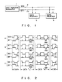
- Fig. 1 shows that data transfer system for use in, for example, a video tape recorder, which transmits data from a microcomputer incorporated in the recorder to an integrated circuit for controlling a servomotor incorporated therein.
- reference numeral 1 denotes a data transfer apparatus for transmitting transfer clock signals SCK1 and binary transfer data signals SDT1, reference numerals 2 and 2a a clock signal-transfer line and a data signal-transfer line, both connected to the data transfer apparatus 1, and reference numeral 3 a plurality of data-receiving terminal units for receiving the transfer clock signals SCK1 and binary transfer data signals SDT1 transmitted through the lines 2 and 2a.
- the data transfer apparatus 1 At the start of transmission of the transfer data signal SDT1, the data transfer apparatus 1 generates a transfer start signal START having logic levels which are different at times corresponding to the leading edge and trailing edge of a clock signal SCK1.
- the apparatus 1 During the transmission of the signal SDT1, the apparatus 1 generates, in serial order, signals SDT1 having logic levels which are identical at times corresponding to the leading edge and trailing edge of each clock signal SCKP1.
- the logic level of the transfer data signal SDT1 is usually inverted at a time between the trailing edge of a certain one of the transfer clock signals SCK1 and the leading edge of the following one.
- the apparatus 1 At the end of transmission, the apparatus 1 generates a transfer end signal END having logic levels inverted at times corresponding to the leading edge and trailing edge of the clock signal SCK1. It should be noted that the logic level of the transfer end signal END changes in the opposite way to that of the transfer start signal START.
- a - D of Fig. 2 show four examples of the relationship between the logic level of the transfer data signal SDT1 and the leading and trailing edges of the transfer clock signal SCK1.
- a of Fig. 2 shows one example.
- the transfer data signal SDT1 has a low level "L” at the rise of the transfer clock signal SCK1, and a high level “H” at the fall of the same.
- a signal of low level "L” containing 2-bit data is transmitted, and then a signal of high level "H” containing 2-bit data is transmitted.
- the level of the signal SDT1 is high at the rise of the transfer clock signal SCK1, and becomes low at the fall of the same.
- FIG. B of Fig. 2 shows another example.
- the level of the transfer data signal SDT1 is high at the rise of the transfer clock signal SCK1, and becomes low at the fall of the same.
- a signal of low level "L” containing 2-bit data is transmitted, and then a signal of high level "H” containing 2-bit data is transmitted.
- the level of the signal SDT1 is low at the rise of the transfer clock signal SCK1, and becomes high at the fall of the same.
- the level of the transfer data signal SDT1 is low at the fall of the transfer clock signal SCK1, and becomes high at the rise of the same.
- a signal of low level "L” containing 2-bit data is transmitted, and then a signal of high level "H” containing 2-bit data is transmitted.
- the level of the signal SDT1 is high at the fall of the transfer clock signal SCK1, and becomes low at the rise of the same.
- the level of the transfer data signal SDT1 is high at the fall of the transfer clock signal SCK1, and becomes low at the rise of the same.
- a signal of low level "L” containing 2-bit data is transmitted, and then a signal of high level "H” containing 2-bit data is transmitted.
- the level of the signal SDT1 is low at the fall of the transfer clock signal SCK1, and becomes high at the rise of the same.
- the data-receiving terminal units 3 have signal-receiving terminals connected to the transfer lines 2 and 2a, and is constructed as follows:
- the transfer data signal SDT1 and transfer clock signal SCK1 transmitted from the data transfer apparatus 1 are hereinafter referred to as “received data signal SDT2" and “received clock signal SCK2", respectively.
- the unit 3 regards the signal as the transfer start signal START, and starts to receive the following signals. Subsequently, when it detects that the logic level of the following received data signal SDT2 is not changed between the leading edge and trailing edge of the received clock signal SCK2, it regards the signal as a received data signal D0. Further, when it detects that the logic level of the received data signal SDT2 has been changed from the second value to the first value between the leading edge and trailing edge of the received clock signal SCK2, it regards the signal as the transfer end signal END.
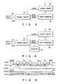
- Fig. 3 shows an example of the data receiving terminal unit 3 comprising an integrated circuit.
- Reference numerals 30 and 30a denote a clock-receving terminal and a data-receiving terminal which are connected to the transfer lines 2 and 2a, respectively.
- a timing circuit 31 receives the clock signal SCK2 and serial data signal SDT2 through the receiving terminals 30 and 30a. Upon detection of the transfer start signal START, the circuit 31 starts to receive the following signals. Then, upon receipt of the following clock signal SCK2 and serial data signal SDT2, it generates clock signals SCKA and a data signals SDTA. Further, upon detection of the transfer end signal END, it stops generating the signals SCKA and SDTA, and simultaneously activates a latch signal LATCH.
- a shift register 32 receives the data signals SDTA in serial order and in synchronism with the respective leading edges of the clock pulses SCKA.
- a latch circuit 33 latches the data transmitted from the shift register 32, also decodes the serial data to parallel data, and further transmits them to a circuit contained in the integrated circuit.
- the data receiving terminal unit 3 may be modified such that it detects the number of bits of data transmitted from the generation of the transfer start signal START to that of the transfer end signal END by counting the clock signals SCKA by means of a counter 34, and receives the transfer data only if the number of the bits counted meets a predetermined value.
- a plurality of data receiving terminal units 3 can select respective particular data, if each unit is set to receive that signal of a particular number of bits which indicates a corresponding data.
- Fig. 5 shows the operation of the data receiving terminal unit 3 performed when it receives those clock signals SCK1 and serial data signals SDT1 which are transmitted from the data transfer apparatus 1 at the timing shown in A of Fig. 2.
- the unit 3 regards the received data signal SDT2 as the transfer start signal START when it detects that the level of the signal SDT2 has changed from the "L" level to the "H” level between the leading edge and trailing edge of the received clock signal SCK2.
- the latch signal LATCH is made inactive.
- the received data signal SDT2 is regarded as the transfer data signal D0 while the unit 3 detects that the level of the signal SDT2 is unchanged between the leading edge and trailing edge of the received clock signal SCK2.
- the transfer data signals D0 - Dn are output after the transfer start signal START is inactivated.
- the signal SDT2 is regarded as the transfer end signal END when the level of the signal SDT2 is detected to change from the "H” level to the "L” level between the leading edge and trailing edge of the received clock signal SCK2, thereby activating the latch signal LATCH.
- hatched portions shown in Fig. 5 indicates time periods in which the logic level is maintained as it is.
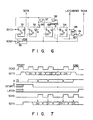
- Fig. 6 shows a specific structure of the timing circuit 31 shown in Fig. 3.
- Reference numerals 51 - 54 denote D-type flip-flop circuits, numerals 55 and 56 inventors, numeral 57 an AND gate having two input terminals, numeral 58 a NOR gate having two input terminals, numerals 59 and 60 NOR gates each having two input terminals and one output terminal, and numeral 61 a NOR gate having three input terminals.
- the output terminal of one of the NOR gates is connected to one of the input terminals of the other NOR gate, while the output terminal of the second-mentioned gate is connected to one of the input terminals of the first-mentioned gate.
- the first flip-flop circuit 51 has a data input terminal D for receiving the data signal SDT2, a clock input terminal CK for receiving an inverted clock signal SCK obtained by inverting the received clock signal SCK2 by the invertor 55, and an output terminal Q for outputting the data signal SDTA.
- the second flip-flop circuit 52 has a data input terminal D for receiving the data signal SDT2, a clock input terminal CK for receiving the clock signal SCK2, and an output terminal Q.
- a signal A output from the terminal Q is inverted by the invertor 56, and then input into the AND gate 57, together with the received data signal SDT2.
- the output from the invertor 56 is input into the NOR gate, together with the received data signal SDT2.
- the third flip-flop circuit 53 has a data input terminal D for receiving the output of the AND gate 57, a clock input terminal CK for receiving the inverted clock signal SCK , and an output terminal Q for outputting a signal B (the transfer start signal START).
- the signal B is input into the NOR gate 61, together with the inverted clock signal SCK .
- the fourth flip-flop circuit 54 has a data input terminal D for receiving the output of the NOR gate, a clock input terminal CK for receiving the inverted clock signal SCK , and an output terminal Q for outputting the latch signal LATCH.
- One of the two input terminals of the NOR gate 59 receives the latch signal LATCH (transfer end signal END), and one of two input terminals of the NOR gate 60 receives the signal B (transfer start signal START).
- the output of the NOR gate 60 is input into the NOR gate 61, which in turn outputs the clock signal SCKA.
- Fig. 7 shows waveforms useful in explaining the operation of the timing circuit 31 shown in Fig. 6.
- the circuit 31 starts signal reception upon detection of the transfer start signal START. Subsequently, it generates, upon detection of the received clock signal SCK2 and serial data signals SDT2, the clock signal SCKA (having the same phase as the clock signal SCK) and the data signal SDTA (this signal is 180°, out of phase with respect to the clock signal SCK, and varies at the time corresponding to the trailing edge of the clock signal SCK). Then, when the circuit 31 detects the transfer end signal END, it stops the generation of the clock signal SCKA and data signal SDTA, and simultaneously activates the latch signal LATCH.
- the present invention can be modified, as shown in A - D of Fig. 2, such that the transfer apparatus 1 transmits a sub-data SBD whose logic level is inverted temporarily between the leading and trailing edges of the transfer clock signal SCK1, and the receiving terminal unit 3 detects whether or not the data signal is temporarily inverted therebetween, thereby enabling the transmission of the sub-data SBD, as well as the main data SDT.
Landscapes
- Engineering & Computer Science (AREA)
- Theoretical Computer Science (AREA)
- Physics & Mathematics (AREA)
- General Engineering & Computer Science (AREA)
- General Physics & Mathematics (AREA)
- Computer Networks & Wireless Communication (AREA)
- Signal Processing (AREA)
- Information Transfer Systems (AREA)
- Synchronisation In Digital Transmission Systems (AREA)
- Communication Control (AREA)
- Dc Digital Transmission (AREA)
Abstract
Description
- This invention relates to a data transfer system for use in, for example, a video tape recorder, which transfers data from a microcomputer incorporated in the recorder to an integrated circuit for controlling a servomotor incorporated therein.
- Published Unexamined Japanese Patent Application No. 57-106262 discloses two types of data transfer systems. The first type employs two transfer lines for transmitting a clock signal and a data signal, respectively. The second type is identical to the first type, except that it has one more line for controlling the start and finish of data transmission.
- More specifically, the first-type system comprises a data transfer apparatus for transmitting clock signals and binary serial-data signals, a bidirectional bus having two lines connected to the data transfer apparatus, and a plurality of data transfer/receiving terminal units connected to the bus. Each of the terminal units has two terminals, one for receiving a signal from the bidirectional bus, and the other for transmitting a signal in reply to the signal received.
- Since each of the data transfer/receiving terminal units requires transfer/receiving terminals connected to the bus, respectively, the system inevitably has a complex hardware structure.
- Further, the data transfer apparatus transmits a data signal which has identical logic levels at times corresponding to the leading and trailing edges of a clock signal, but does not transmit a sub-data signal which has logic levels temporarily inverted at any time between the leading and trailing edges of the clock signal. With this structure, it is impossible to transmit lots of data.
- On the other hand, the second-type system requires as many as three transfer lines.
- It is the object of the invention to provide a data transfer system which employs two transfer lines, and data receiving terminal units having only receiving terminals for the lines, resulting in a simple hardware structure, and to provide a data transfer method which enables the system of simple structure to accurately control the start and finish of data transmission.
- To attain the above object, the data transfer system of the invention comprises:
a data transfer apparatus (1) for transmitting clock signals (SCK₁) and binary data signals (SDT₁), the data signals being transmitted in serial order, of which a signal transmitted at the start has a first logic level at a time corresponding to a leading edge of a clock signal (SCK₁) and a second logic level at a time corresponding to a trailing edge of the same, signals transmitted after the start have identical logic levels at times corresponding to the leading edge and trailing edge of the transfer clock signal, and a signal transmitted at the edge has the second level at the time corresponding to the leading edge of the clock signal and the first logic level at the time corresponding to the trailing edge of the same;
a clock signal-tranfer line (2) connected to the data transfer apparatus (1);
a data signal-transfer line (2a) connected to the data transfer apparatus (1); and
at least one data receiving terminal unit (3) connected to the clock signal-transfer line (2) and data signal-transfer line (2a), the data receiving terminal unit (3) regarding the data signal (SDT₂) transmitted from data transfer apparatus (1) as a transfer start signal (START) when it detects that the data signal (SDT₂) transmitted at the time corresponding to the leading edge of the clock signal (SCK₂) transmitted from the apparatus (1) has the first logic level, and that the data signal (SDT₂) transmitted at the time corresponding to the trailing edge of the same has the second logic level, also regarding the data signal (SDT₂) as a transfer data signal when it detects that the data signal (SDT₂) transmitted at the time corresponding to the leading edge of the clock signal (SCK₂) has the same logic level as that transmitted at the time corresponding to the trailing edge of the same, and further regarding the data signal (SDT₂) as a transfer end signal (END) when it detects that the data signal (SDT₂) transmitted at the time corresponding to the leading edge of the clock signal (SCK₂) has the second logic level, and that the data signal (SDT₂) transmitted at the time corresponding to the trailing edge of the same has the first logic level. - According to another aspect of the invention, a method of transmitting data is provided which comprises the steps of:
transmitting clock signals (SCK₁) from a data transfer apparatus (1) to at least one receiving terminal unit (3) connected to the apparatus (1) via a clock signal-transfer line (2);
transmitting binary data signals (SDT₁) in serial order from the data transfer apparatus (1) to the receiving terminal unit (3) connected to the apparatus (1) via a data signal-transfer line (2a);
making the data transfer apparatus (3) regard the data signal (SDT₂) transmitted from data transfer apparatus (1) as a transfer start signal (START) when the apparatus (3) detects that the data signal (SDT₂) transmitted at a time corresponding to a leading edge of a clock signal (SCK₂) transmitted from the apparatus (1) has a first logic level, and that the data signal (SDT₂) transmitted at a time corresponding to a trailing edge of the same has a second logic level;
making the apparatus (3) regard the data signal (SDT₂) as a transfer data signal when it detects that the data signal (SDT₂) transmitted at the time corresponding to the leading edge of the clock signal (SCK₂) has the same logic level as that transmitted at the time corresponding to the trailing edge of the same; and
making the apparatus (3) regard the data signal (SDT₂) as a transfer end signal (END) when it detects that the data signal (SDT₂) transmitted at the time corresponding to the leading edge of the clock signal (SCK₂) has the second logic level, and that the data signal (SDT₂) transmitted at the time corresponding to the trailing edge of the same has the first logic level. - According to the invention constructed as above, the start time of data transmission, the end time thereof, and the time therebetween are determined by comparing logic levels of a data signal (SDT₂) assumed at times corresponding to the leading and trailing edges of a clock signal (SCK₂), so that the start and end of the data transmission can be controlled by using only two transfer lines (2, 2a). In addition, each data receiving terminal unit (3) has only receiving terminals connected to the transfer lines (2, 2a), resulting in a simple hardware structure.
- This invention can be more fully understood from the following detailed description when taken in conjunction with the accompanying drawings, in which:
- Fig. 1 is a block diagram, showing a data transfer apparatus according to an embodiment of the present invention; A - D of Fig. 2 are waveform charts, showing the relationship between the logic levels of data signals transmitted from the data transfer apparatus shown in Fig. 1 and the leading/trailing edges of clock signals transmitted from the same;
- Fig. 3 is a circuit diagram of a data receiver shown in Fig. 1;
- Fig. 4 is a circuit diagram of another data receiver shown in Fig. 1;
- Fig. 5 is a waveform chart, showing the operation of data receiving terminal units shown in Figs. 3 and 4;
- Fig. 6 is a circuit diagram of a timing circuit shown in Figs. 3 and 4; and
- Fig. 7 is a waveform chart, showing the operation of the timing circuit shown in Fig. 6.
- The invention will now be explained in detail with reference to the accompanying drawings showing an embodiment thereof.
- Fig. 1 shows that data transfer system for use in, for example, a video tape recorder, which transmits data from a microcomputer incorporated in the recorder to an integrated circuit for controlling a servomotor incorporated therein. In the figure,
reference numeral 1 denotes a data transfer apparatus for transmitting transfer clock signals SCK₁ and binary transfer data signals SDT₁,reference numerals 2 and 2a a clock signal-transfer line and a data signal-transfer line, both connected to thedata transfer apparatus 1, and reference numeral 3 a plurality of data-receiving terminal units for receiving the transfer clock signals SCK₁ and binary transfer data signals SDT₁ transmitted through thelines 2 and 2a. - At the start of transmission of the transfer data signal SDT₁, the
data transfer apparatus 1 generates a transfer start signal START having logic levels which are different at times corresponding to the leading edge and trailing edge of a clock signal SCK₁. During the transmission of the signal SDT₁, theapparatus 1 generates, in serial order, signals SDT₁ having logic levels which are identical at times corresponding to the leading edge and trailing edge of each clock signal SCKP₁. The logic level of the transfer data signal SDT₁ is usually inverted at a time between the trailing edge of a certain one of the transfer clock signals SCK₁ and the leading edge of the following one. At the end of transmission, theapparatus 1 generates a transfer end signal END having logic levels inverted at times corresponding to the leading edge and trailing edge of the clock signal SCK₁. It should be noted that the logic level of the transfer end signal END changes in the opposite way to that of the transfer start signal START. - The above-described structure of the
data transfer apparatus 1 comprising a microcomputer or the like is known to those skilled in the art. - A - D of Fig. 2 show four examples of the relationship between the logic level of the transfer data signal SDT₁ and the leading and trailing edges of the transfer clock signal SCK₁. Specifically, A of Fig. 2 shows one example. In the figure, at the start of the transmission, the transfer data signal SDT₁ has a low level "L" at the rise of the transfer clock signal SCK₁, and a high level "H" at the fall of the same. During the transmission, for example, a signal of low level "L" containing 2-bit data is transmitted, and then a signal of high level "H" containing 2-bit data is transmitted. At the end of the transfer, the level of the signal SDT₁ is high at the rise of the transfer clock signal SCK₁, and becomes low at the fall of the same.
- B of Fig. 2 shows another example. At the start of the transmission, the level of the transfer data signal SDT₁ is high at the rise of the transfer clock signal SCK₁, and becomes low at the fall of the same. During the transmission, for example, a signal of low level "L" containing 2-bit data is transmitted, and then a signal of high level "H" containing 2-bit data is transmitted. At the end of the transmission, the level of the signal SDT₁ is low at the rise of the transfer clock signal SCK₁, and becomes high at the fall of the same.
- Further, as is shown in C of Fig. 2, at the start of the transfer, the level of the transfer data signal SDT₁ is low at the fall of the transfer clock signal SCK₁, and becomes high at the rise of the same. During the transmission, for example, a signal of low level "L" containing 2-bit data is transmitted, and then a signal of high level "H" containing 2-bit data is transmitted. At the end of the transmission, the level of the signal SDT₁ is high at the fall of the transfer clock signal SCK₁, and becomes low at the rise of the same.
- Finally, as is shown in D of Fig. 2, at the start of the transmission, the level of the transfer data signal SDT₁ is high at the fall of the transfer clock signal SCK₁, and becomes low at the rise of the same. During the transmission, for example, a signal of low level "L" containing 2-bit data is transmitted, and then a signal of high level "H" containing 2-bit data is transmitted. At the end of the transmission, the level of the signal SDT₁ is low at the fall of the transfer clock signal SCK₁, and becomes high at the rise of the same.
- In A - D of Fig. 2, if the logic level of the transfer data signal SDT₁ is temporarily inverted between the leading and trailing edges of the transfer clock signal SCK₁, the data can be considered normal.
- The data-receiving
terminal units 3 have signal-receiving terminals connected to thetransfer lines 2 and 2a, and is constructed as follows: - The transfer data signal SDT₁ and transfer clock signal SCK₁ transmitted from the
data transfer apparatus 1 are hereinafter referred to as "received data signal SDT₂" and "received clock signal SCK₂", respectively. When each data-receivingterminal unit 3 detects that the logic level of the received data signal SDT₂ has been changed from a first value to a second value between the leading edge and trailing edge of the received clock signal SCK₂, theunit 3 regards the signal as the transfer start signal START, and starts to receive the following signals. Subsequently, when it detects that the logic level of the following received data signal SDT₂ is not changed between the leading edge and trailing edge of the received clock signal SCK₂, it regards the signal as a received data signal D₀. Further, when it detects that the logic level of the received data signal SDT₂ has been changed from the second value to the first value between the leading edge and trailing edge of the received clock signal SCK₂, it regards the signal as the transfer end signal END. - Fig. 3 shows an example of the data receiving
terminal unit 3 comprising an integrated circuit.Reference numerals transfer lines 2 and 2a, respectively. Atiming circuit 31 receives the clock signal SCK₂ and serial data signal SDT₂ through thereceiving terminals circuit 31 starts to receive the following signals. Then, upon receipt of the following clock signal SCK₂ and serial data signal SDT₂, it generates clock signals SCKA and a data signals SDTA. Further, upon detection of the transfer end signal END, it stops generating the signals SCKA and SDTA, and simultaneously activates a latch signal LATCH. Ashift register 32 receives the data signals SDTA in serial order and in synchronism with the respective leading edges of the clock pulses SCKA. Upon activation of the latch signal LATCH, alatch circuit 33 latches the data transmitted from theshift register 32, also decodes the serial data to parallel data, and further transmits them to a circuit contained in the integrated circuit. - As is shown in Fig. 4, the data receiving
terminal unit 3 may be modified such that it detects the number of bits of data transmitted from the generation of the transfer start signal START to that of the transfer end signal END by counting the clock signals SCKA by means of acounter 34, and receives the transfer data only if the number of the bits counted meets a predetermined value. In this case, a plurality of data receivingterminal units 3 can select respective particular data, if each unit is set to receive that signal of a particular number of bits which indicates a corresponding data. - Fig. 5 shows the operation of the data receiving
terminal unit 3 performed when it receives those clock signals SCK₁ and serial data signals SDT₁ which are transmitted from thedata transfer apparatus 1 at the timing shown in A of Fig. 2. Theunit 3 regards the received data signal SDT₂ as the transfer start signal START when it detects that the level of the signal SDT₂ has changed from the "L" level to the "H" level between the leading edge and trailing edge of the received clock signal SCK₂. Upon generation of the signal START, the latch signal LATCH is made inactive. Then, the received data signal SDT₂ is regarded as the transfer data signal D₀ while theunit 3 detects that the level of the signal SDT₂ is unchanged between the leading edge and trailing edge of the received clock signal SCK₂. The transfer data signals D₀ - Dn are output after the transfer start signal START is inactivated. The signal SDT₂ is regarded as the transfer end signal END when the level of the signal SDT₂ is detected to change from the "H" level to the "L" level between the leading edge and trailing edge of the received clock signal SCK₂, thereby activating the latch signal LATCH. - The hatched portions shown in Fig. 5 indicates time periods in which the logic level is maintained as it is.
- Fig. 6 shows a specific structure of the
timing circuit 31 shown in Fig. 3. Reference numerals 51 - 54 denote D-type flip-flop circuits,numerals numerals flop circuit 51 has a data input terminal D for receiving the data signal SDT₂, a clock input terminal CK for receiving an inverted clock signalSCK obtained by inverting the received clock signal SCK₂ by theinvertor 55, and an output terminal Q for outputting the data signal SDTA. The second flip-flop circuit 52 has a data input terminal D for receiving the data signal SDT₂, a clock input terminal CK for receiving the clock signal SCK₂, and an output terminal Q. A signal A output from the terminal Q is inverted by theinvertor 56, and then input into the ANDgate 57, together with the received data signal SDT₂. The output from theinvertor 56 is input into the NOR gate, together with the received data signal SDT₂. The third flip-flop circuit 53 has a data input terminal D for receiving the output of the ANDgate 57, a clock input terminal CK for receiving the inverted clock signalSCK , and an output terminal Q for outputting a signal B (the transfer start signal START). The signal B is input into the NORgate 61, together with the inverted clock signalSCK . The fourth flip-flop circuit 54 has a data input terminal D for receiving the output of the NOR gate, a clock input terminal CK for receiving the inverted clock signalSCK , and an output terminal Q for outputting the latch signal LATCH. One of the two input terminals of the NORgate 59 receives the latch signal LATCH (transfer end signal END), and one of two input terminals of the NORgate 60 receives the signal B (transfer start signal START). The output of the NORgate 60 is input into the NORgate 61, which in turn outputs the clock signal SCKA. - Fig. 7 shows waveforms useful in explaining the operation of the
timing circuit 31 shown in Fig. 6. Thecircuit 31 starts signal reception upon detection of the transfer start signal START. Subsequently, it generates, upon detection of the received clock signal SCK₂ and serial data signals SDT₂, the clock signal SCKA (having the same phase as the clock signal SCK) and the data signal SDTA (this signal is 180°, out of phase with respect to the clock signal SCK, and varies at the time corresponding to the trailing edge of the clock signal SCK). Then, when thecircuit 31 detects the transfer end signal END, it stops the generation of the clock signal SCKA and data signal SDTA, and simultaneously activates the latch signal LATCH. - In the above-described embodiment, although the data signal SDT₁ is transmitted which has logic levels being identical between the leading edge and trailing edge of the transfer clock signal SCK₁, the present invention can be modified, as shown in A - D of Fig. 2, such that the
transfer apparatus 1 transmits a sub-data SBD whose logic level is inverted temporarily between the leading and trailing edges of the transfer clock signal SCK₁, and the receivingterminal unit 3 detects whether or not the data signal is temporarily inverted therebetween, thereby enabling the transmission of the sub-data SBD, as well as the main data SDT. - Reference signs in the claims are intended for better understanding and shall not limit the scope.
Claims (6)
- A data transfer apparatus characterized by comprising:
a data transfer means (1) for transmitting clock signals (SCK₁) and binary data signals (SDT₁), the data signals being transmitted in serial order, of which a signal transmitted at the start has a first logic level at a time corresponding to a leading edge of a clock signal (SCK₁) and a second logic level at a time corresponding to a trailing edge of the same, signals transmitted after the start have identical logic levels at times corresponding to the leading edge and trailing edge of the transfer clock signal, and a signal transmitted at the end has the second level at the time corresponding to the leading edge of the clock signal and the first logic level at the time corresponding to the trailing edge of the same;
a clock signal-tranfer line (2) connected to the data transfer means (1);
a data signal-transfer line (2a) connected to the data transfer means (1); and
at least one data receiving terminal unit (3) connected to the clock signal-transfer line (2) and data signal-transfer line (2a), the data receiving terminal unit (3) regarding the data signal (SDT₂) transmitted from data transfer means (1) as a transfer start signal (START) when it detects that the data signal (SDT₂) transmitted at the time corresponding to the leading edge of the clock signal (SCK₂) transmitted from the means (1) has the first logic level, and that the data signal (SDT₂) transmitted at the time corresponding to the trailing edge of the same has the second logic level, also regarding the data signal (SDT₂) as a transfer data signal when it detects that the data signal (SDT₂) transmitted at the time corresponding to the leading edge of the clock signal (SCK₂) has the same logic level as that transmitted at the time corresponding to the trailing edge of the same, and further regarding the data signal (SDT₂) as a transfer end signal (END) when it detects that the data signal (SDT₂) transmitted at the time corresponding to the leading edge of the clock signal (SCK₂) has the second logic level, and that the data signal (SDT₂) transmitted at the time corresponding to the trailing edge of the same has the first logic level. - The apparatus according to claim 1, characterized in that the receiving terminal unit (3) comprises a timing circuit (31) for receiving the clock signals (SCK₁) and the data signals (SDT₁) which are transmitted from the data transfer means (1) through the clock signal-transfer line (2) and the data signal-transfer line (2a), respectively, the timing circuit (31) starting data reception upon detection of the transfer start signal (START), also generating clock signals (SCKA) and data signals (SDTA) corresponding to the received clock signals (SCK₂) and the received data signals (SDT₂) upon detection thereof, and further stopping the generation of the clock signals (SCKA) and the data signals (SDTA) upon detection of the transfer end signal (END), and simultaneously activating a latch signal (LATCH), the system further comprising a shift register (32) for receiving the data signals (SDTA) in serial order at times corresponding to the leading edge of the clock signal (SCKA), and a latch circuit (33) for latching data transmitted from the shift register (32) upon activation of the latch signal (LATCH), and decoding the serial data into parallel data.
- The apparatus according to claim 2, characterized in that the receiving terminal unit (3) further comprises a counter (34) for counting the clock signals (SCKA) generated by the timing circuit (31), thereby detecting the number of bits of data transmitted from the time at which the transfer start signal (START) is detected to the time at which the transfer end signal (END) is detected, and the receiving terminal unit (3) receives the data signals (SDT₁) transmitted from the data transfer means (1) only if the bit number detected is a predetermined value.
- A method of transmitting data, comprising the steps of:
transmitting clock signals (SCK₁) from a data transfer means (1) to at least one receiving terminal unit (3) connected to the means (1) via a clock signal-transfer line (2);
transmitting binary data signals (SDT₁) in serial order from the data transfer apparatus (1) to the receiving terminal unit (3) connected to the means (1) via a data signal-transfer line (2a);
making the data transfer apparatus (3) regard the data signal (SDT₂) transmitted from data transfer means (1) as a transfer start signal (START) when the apparatus (3) detects that the data signal (SDT₂) transmitted at a time corresponding to a leading edge of a clock signal (SCK₂) transmitted from the means (1) has a first logic level, and that the data signal (SDT₂) transmitted at a time corresponding to a trailing edge of the same has a second logic level;
making the apparatus (3) regard the data signal (SDT₂) as a transfer data signal when it detects that the data signal (SDT₂) transmitted at the time corresponding to the leading edge of the clock signal (SCK₂) has the same logic level as that transmitted at the time corresponding to the trailing edge of the same; and
making the apparatus (3) regard the data signal (SDT₂) as a transfer end signal (END) when it detects that the data signal (SDT₂) transmitted at the time corresponding to the leading edge of the clock signal (SCK₂) has the second logic level, and that the data signal (SDT₂) transmitted at the time corresponding to the trailing edge of the same has the first logic level. - The method according to claim 4, characterized in that the receiving terminal unit (3) comprises a timing circuit (31) for receiving the clock signals (SCK₁) and the data signals (SDT₁) which are transmitted from the data transfer means (1) through the clock signal-transfer line (2) and the data signal-transfer line (2a), respectively, the timing circuit (31) starting data reception upon detection of the transfer start signal (START), also generating clock signals (SCKA) and data signals (SDTA) corresponding to the received clock signals (SCK₂) and the received data signals (SDT₂) upon detection thereof, and further stopping the generation of the clock signals (SCKA) and the data signals (SDTA) upon detection of the transfer end signal (END), and simultaneously activating a latch signal (LATCH), the system further comprising a shift register (32) for receiving the data signals (SDTA) in serial order at times corresponding to the leading edge of the clock signal (SCKA), and a latch circuit (33) for latching data transmitted from the shift register (32) upon activation of the latch signal (LATCH), and decoding the serial data into parallel data.
- The method according to claim 5, characterized in that the receiving terminal unit (3) further comprises a counter (34) for counting the clock signals (SCKA) generated by the timing circuit (31), thereby detecting the number of bits of data transmitted from the time at which the transfer start signal (START) is detected to the time at which the transfer end signal (END) is detected, and the receiving terminal unit (3) receives the data signals (SDT₁) transmitted from the data transfer apparatus (1) only if the bit number detected is a predetermined value.
Applications Claiming Priority (2)
| Application Number | Priority Date | Filing Date | Title |
|---|---|---|---|
| JP32970989A JPH0624356B2 (en) | 1989-12-21 | 1989-12-21 | Data transfer method |
| JP329709/89 | 1989-12-21 |
Publications (3)
| Publication Number | Publication Date |
|---|---|
| EP0434083A2 true EP0434083A2 (en) | 1991-06-26 |
| EP0434083A3 EP0434083A3 (en) | 1992-03-04 |
| EP0434083B1 EP0434083B1 (en) | 1996-09-11 |
Family
ID=18224397
Family Applications (1)
| Application Number | Title | Priority Date | Filing Date |
|---|---|---|---|
| EP90125083A Expired - Lifetime EP0434083B1 (en) | 1989-12-21 | 1990-12-21 | Data transfer system and method of transferring data |
Country Status (5)
| Country | Link |
|---|---|
| US (1) | US5142556A (en) |
| EP (1) | EP0434083B1 (en) |
| JP (1) | JPH0624356B2 (en) |
| KR (1) | KR940002144B1 (en) |
| DE (1) | DE69028498T2 (en) |
Cited By (4)
| Publication number | Priority date | Publication date | Assignee | Title |
|---|---|---|---|---|
| EP0718778A1 (en) * | 1994-12-21 | 1996-06-26 | Philips Electronique Grand Public | Method of transmission of data on a bus |
| EP1096745A2 (en) * | 1999-10-29 | 2001-05-02 | Rohm Co., Ltd. | Serial data transfer method in synchronism with a clock signal |
| GB2365723A (en) * | 2000-02-22 | 2002-02-20 | Nec Corp | Serial to parallel conversion by extracting even and odd numbered data pulses synchronously with leading and trailing edges of clock pulses respectively |
| WO2006054226A2 (en) * | 2004-11-16 | 2006-05-26 | Koninklijke Philips Electronics N.V. | Bus communication system |
Families Citing this family (14)
| Publication number | Priority date | Publication date | Assignee | Title |
|---|---|---|---|---|
| JPH0522262A (en) * | 1991-06-21 | 1993-01-29 | Matsushita Electric Ind Co Ltd | Data transmission system, transmitter, receiver and transmission control system |
| US5548620A (en) * | 1994-04-20 | 1996-08-20 | Sun Microsystems, Inc. | Zero latency synchronized method and apparatus for system having at least two clock domains |
| US5798667A (en) * | 1994-05-16 | 1998-08-25 | At&T Global Information Solutions Company | Method and apparatus for regulation of power dissipation |
| US5534796A (en) * | 1995-04-21 | 1996-07-09 | Intergraph Corporation | Self-clocking pipeline register |
| GB9713079D0 (en) | 1997-06-21 | 1997-08-27 | T & N Technology Ltd | Manufacture of plain bearings |
| IL138411A (en) | 1998-03-16 | 2005-11-20 | Jazio Inc | High speed bus system and method for using voltageand timing oscillating references for signal detection |
| US6160423A (en) * | 1998-03-16 | 2000-12-12 | Jazio, Inc. | High speed source synchronous signaling for interfacing VLSI CMOS circuits to transmission lines |
| US6892252B2 (en) | 2000-09-21 | 2005-05-10 | Michael Tate | Asymmetric data path media access controller |
| US7123660B2 (en) * | 2001-02-27 | 2006-10-17 | Jazio, Inc. | Method and system for deskewing parallel bus channels to increase data transfer rates |
| JP3637014B2 (en) * | 2001-11-21 | 2005-04-06 | 日本電気株式会社 | Clock synchronization loss detection circuit and optical receiver using the same |
| JP2006040149A (en) * | 2004-07-29 | 2006-02-09 | Toshiba Corp | Semiconductor integrated circuit device |
| KR100632952B1 (en) * | 2004-09-30 | 2006-10-11 | 삼성전자주식회사 | Method and device capable of judging whether program operation is failed due to power failure |
| DE102006006833B4 (en) * | 2006-02-14 | 2008-07-17 | Infineon Technologies Ag | Method for transmitting digital information, and signal modulation and signal demodulation device |
| KR100866603B1 (en) * | 2007-01-03 | 2008-11-03 | 삼성전자주식회사 | Data processing method and apparatus for performing deserializing and serializing |
Citations (3)
| Publication number | Priority date | Publication date | Assignee | Title |
|---|---|---|---|---|
| EP0154774A2 (en) * | 1984-02-10 | 1985-09-18 | Deutsche Thomson-Brandt GmbH | Data transmission with a bidirectionel data bus |
| EP0258873A2 (en) * | 1986-09-01 | 1988-03-09 | Nec Corporation | Serial bus interface system for data communication using two-wire line as clock bus and data bus |
| EP0266790A2 (en) * | 1986-11-06 | 1988-05-11 | Nec Corporation | Serial bus interface capable of transferring data in different formats |
Family Cites Families (4)
| Publication number | Priority date | Publication date | Assignee | Title |
|---|---|---|---|---|
| JPS5949044A (en) * | 1982-09-13 | 1984-03-21 | Fuji Electric Co Ltd | Data communication method |
| JPS63197151A (en) * | 1987-02-12 | 1988-08-16 | Hitachi Ltd | Serial data transfer system |
| US4782481A (en) * | 1987-02-24 | 1988-11-01 | Hewlett-Packard Company | Apparatus and method for transferring information |
| JPH0786855B2 (en) * | 1987-04-15 | 1995-09-20 | 日本電気株式会社 | Serial data processing device |
-
1989
- 1989-12-21 JP JP32970989A patent/JPH0624356B2/en not_active Expired - Fee Related
-
1990
- 1990-12-18 KR KR1019900020857A patent/KR940002144B1/en not_active IP Right Cessation
- 1990-12-19 US US07/630,243 patent/US5142556A/en not_active Expired - Lifetime
- 1990-12-21 EP EP90125083A patent/EP0434083B1/en not_active Expired - Lifetime
- 1990-12-21 DE DE69028498T patent/DE69028498T2/en not_active Expired - Fee Related
Patent Citations (3)
| Publication number | Priority date | Publication date | Assignee | Title |
|---|---|---|---|---|
| EP0154774A2 (en) * | 1984-02-10 | 1985-09-18 | Deutsche Thomson-Brandt GmbH | Data transmission with a bidirectionel data bus |
| EP0258873A2 (en) * | 1986-09-01 | 1988-03-09 | Nec Corporation | Serial bus interface system for data communication using two-wire line as clock bus and data bus |
| EP0266790A2 (en) * | 1986-11-06 | 1988-05-11 | Nec Corporation | Serial bus interface capable of transferring data in different formats |
Cited By (10)
| Publication number | Priority date | Publication date | Assignee | Title |
|---|---|---|---|---|
| EP0718778A1 (en) * | 1994-12-21 | 1996-06-26 | Philips Electronique Grand Public | Method of transmission of data on a bus |
| FR2728705A1 (en) * | 1994-12-21 | 1996-06-28 | Philips Electronics Nv | DATA TRANSMISSION PROCEDURE BY BUS |
| EP1096745A2 (en) * | 1999-10-29 | 2001-05-02 | Rohm Co., Ltd. | Serial data transfer method in synchronism with a clock signal |
| EP1096745A3 (en) * | 1999-10-29 | 2006-01-18 | Rohm Co., Ltd. | Serial data transfer method in synchronism with a clock signal |
| GB2365723A (en) * | 2000-02-22 | 2002-02-20 | Nec Corp | Serial to parallel conversion by extracting even and odd numbered data pulses synchronously with leading and trailing edges of clock pulses respectively |
| GB2365723B (en) * | 2000-02-22 | 2002-10-09 | Nec Corp | Data transfer method and system |
| US6898722B2 (en) | 2000-02-22 | 2005-05-24 | Nec Corporation | Parallel data transfer method and system of DDR divided data with associated transfer clock signal over three signal lines |
| WO2006054226A2 (en) * | 2004-11-16 | 2006-05-26 | Koninklijke Philips Electronics N.V. | Bus communication system |
| WO2006054226A3 (en) * | 2004-11-16 | 2006-07-27 | Koninkl Philips Electronics Nv | Bus communication system |
| CN101057229B (en) * | 2004-11-16 | 2010-11-03 | Nxp股份有限公司 | Bus communication system |
Also Published As
| Publication number | Publication date |
|---|---|
| JPH0624356B2 (en) | 1994-03-30 |
| EP0434083A3 (en) | 1992-03-04 |
| KR940002144B1 (en) | 1994-03-18 |
| US5142556A (en) | 1992-08-25 |
| KR910013799A (en) | 1991-08-08 |
| DE69028498D1 (en) | 1996-10-17 |
| EP0434083B1 (en) | 1996-09-11 |
| DE69028498T2 (en) | 1997-02-13 |
| JPH03191633A (en) | 1991-08-21 |
Similar Documents
| Publication | Publication Date | Title |
|---|---|---|
| EP0434083B1 (en) | Data transfer system and method of transferring data | |
| EP0059724B1 (en) | Self-clocking data transmission system | |
| US4887262A (en) | Single-channel bus system for multi-master use with bit cell synchronization, and master station comprising a bit cell synchronization element suitable for this purpose | |
| US4298978A (en) | Data communication apparatus | |
| US4689740A (en) | Two-wire bus-system comprising a clock wire and a data wire for interconnecting a number of stations | |
| EP0051332A1 (en) | Two-wire bus-system comprising a clock wire and a data wire for interconnecting a number of stations | |
| EP0486072A2 (en) | Interface for serial data communications link | |
| EP1650670A1 (en) | Serial bus system | |
| GB1581836A (en) | Cpu-i/o bus interface for a data processing system | |
| EP0400824A2 (en) | Bidirectional communication line buffer apparatus | |
| EP0418776B1 (en) | Controller for effecting a serial data communication and system including the same | |
| EP0196870B1 (en) | Interface circuit for transmitting and receiving data | |
| EP0024940A2 (en) | Method and apparatus for transmission of serial data | |
| US5379327A (en) | Synchronous-to-asynchronous converter | |
| EP0564118B1 (en) | Serial data transfer apparatus | |
| US5193093A (en) | Data transfer process with loop checking | |
| EP1072101B1 (en) | Methods and apparatus for exchanging data | |
| US5502720A (en) | Packet collecting circuit in data-flow type system | |
| US4744024A (en) | Method of operating a bus in a data processing system via a repetitive three stage signal sequence | |
| US5550533A (en) | High bandwidth self-timed data clocking scheme for memory bus implementation | |
| SE515886C2 (en) | Methods of data transfer and data transfer device operating at two frequencies | |
| US7085325B2 (en) | Serial interface unit with transmit monitor | |
| US5559998A (en) | Clock synchronous serial information receiving apparatus receiving reliable information even when noise is present | |
| US7107474B2 (en) | Data transfer unit and method | |
| US4229623A (en) | Receiving means for use in a high speed, low noise digital data communication system |
Legal Events
| Date | Code | Title | Description |
|---|---|---|---|
| PUAI | Public reference made under article 153(3) epc to a published international application that has entered the european phase |
Free format text: ORIGINAL CODE: 0009012 |
|
| 17P | Request for examination filed |
Effective date: 19901221 |
|
| AK | Designated contracting states |
Kind code of ref document: A2 Designated state(s): DE FR GB |
|
| PUAL | Search report despatched |
Free format text: ORIGINAL CODE: 0009013 |
|
| AK | Designated contracting states |
Kind code of ref document: A3 Designated state(s): DE FR GB |
|
| 17Q | First examination report despatched |
Effective date: 19951129 |
|
| GRAH | Despatch of communication of intention to grant a patent |
Free format text: ORIGINAL CODE: EPIDOS IGRA |
|
| GRAH | Despatch of communication of intention to grant a patent |
Free format text: ORIGINAL CODE: EPIDOS IGRA |
|
| GRAA | (expected) grant |
Free format text: ORIGINAL CODE: 0009210 |
|
| AK | Designated contracting states |
Kind code of ref document: B1 Designated state(s): DE FR GB |
|
| REF | Corresponds to: |
Ref document number: 69028498 Country of ref document: DE Date of ref document: 19961017 |
|
| ET | Fr: translation filed | ||
| PLBE | No opposition filed within time limit |
Free format text: ORIGINAL CODE: 0009261 |
|
| STAA | Information on the status of an ep patent application or granted ep patent |
Free format text: STATUS: NO OPPOSITION FILED WITHIN TIME LIMIT |
|
| 26N | No opposition filed | ||
| PGFP | Annual fee paid to national office [announced via postgrant information from national office to epo] |
Ref country code: FR Payment date: 19971209 Year of fee payment: 8 |
|
| PGFP | Annual fee paid to national office [announced via postgrant information from national office to epo] |
Ref country code: GB Payment date: 19971212 Year of fee payment: 8 |
|
| PG25 | Lapsed in a contracting state [announced via postgrant information from national office to epo] |
Ref country code: GB Free format text: LAPSE BECAUSE OF NON-PAYMENT OF DUE FEES Effective date: 19981221 |
|
| GBPC | Gb: european patent ceased through non-payment of renewal fee |
Effective date: 19981221 |
|
| PG25 | Lapsed in a contracting state [announced via postgrant information from national office to epo] |
Ref country code: FR Free format text: LAPSE BECAUSE OF NON-PAYMENT OF DUE FEES Effective date: 19990831 |
|
| REG | Reference to a national code |
Ref country code: FR Ref legal event code: ST |
|
| PGFP | Annual fee paid to national office [announced via postgrant information from national office to epo] |
Ref country code: DE Payment date: 20051215 Year of fee payment: 16 |
|
| PG25 | Lapsed in a contracting state [announced via postgrant information from national office to epo] |
Ref country code: DE Free format text: LAPSE BECAUSE OF NON-PAYMENT OF DUE FEES Effective date: 20070703 |