EP0423036A2 - CPU-bus controller - Google Patents
CPU-bus controller Download PDFInfo
- Publication number
- EP0423036A2 EP0423036A2 EP90402847A EP90402847A EP0423036A2 EP 0423036 A2 EP0423036 A2 EP 0423036A2 EP 90402847 A EP90402847 A EP 90402847A EP 90402847 A EP90402847 A EP 90402847A EP 0423036 A2 EP0423036 A2 EP 0423036A2
- Authority
- EP
- European Patent Office
- Prior art keywords
- input
- output bus
- signals
- bus
- data
- Prior art date
- Legal status (The legal status is an assumption and is not a legal conclusion. Google has not performed a legal analysis and makes no representation as to the accuracy of the status listed.)
- Granted
Links
Images


Classifications
-
- G—PHYSICS
- G06—COMPUTING; CALCULATING OR COUNTING
- G06F—ELECTRIC DIGITAL DATA PROCESSING
- G06F13/00—Interconnection of, or transfer of information or other signals between, memories, input/output devices or central processing units
- G06F13/38—Information transfer, e.g. on bus
-
- G—PHYSICS
- G06—COMPUTING; CALCULATING OR COUNTING
- G06F—ELECTRIC DIGITAL DATA PROCESSING
- G06F13/00—Interconnection of, or transfer of information or other signals between, memories, input/output devices or central processing units
- G06F13/38—Information transfer, e.g. on bus
- G06F13/42—Bus transfer protocol, e.g. handshake; Synchronisation
- G06F13/4204—Bus transfer protocol, e.g. handshake; Synchronisation on a parallel bus
- G06F13/4221—Bus transfer protocol, e.g. handshake; Synchronisation on a parallel bus being an input/output bus, e.g. ISA bus, EISA bus, PCI bus, SCSI bus
- G06F13/423—Bus transfer protocol, e.g. handshake; Synchronisation on a parallel bus being an input/output bus, e.g. ISA bus, EISA bus, PCI bus, SCSI bus with synchronous protocol
Definitions
- the present invention relates to microprocessor bus controllers and in particular to bus controllers incorporating state machine technology to provide a functional link between microprocessors having different size data widths, and a data bus which allows access to devices having different size data widths on the data bus.
- I/O bus input/output system
- a complete I/O bus includes several component parts: the data bus, lines over which data flows; the address bus, a set of lines that specify the memory addresses to which data will be transferred; and various support lines carrying control signals and power for the various devices on the bus.
- a bus controller initiates and controls all I/O bus cycles. The controller controls the interface to the I/O bus, the address and data buffers, the CPU, the direct memory access (DMA) device and other memory controllers.
- DMA direct memory access
- bus controllers were integrated into and functioned as a part of the microprocessor architecture. As microprocessor technology has advanced, bus controller technology has become separate and distinct. Similarly, as the number of peripheral devices available for use with various microprocessors has increased, it has become obvious that peripheral devices usable with one integrated microprocessor-bus controller architecture can not generally be used with the bus controller of another microprocessor.
- microprocessors are expected to interface with memory manage units, CRT controllers, floppy disc controllers, hard disc controllers, arithmetic cove processors and the like.
- memory manage units CRT controllers, floppy disc controllers, hard disc controllers, arithmetic cove processors and the like.
- floppy disc controllers floppy disc controllers
- hard disc controllers arithmetic cove processors and the like.
- arithmetic cove processors and the like.
- the next generation of 32-byte microprocessors must be able to interface with already existing peripheral devices without the immediate need for specifically designed bus controllers.
- bus controllers designed to interface with a specific type or range of types of microprocessors and peripheral devices are still limited to certain system configurations and further limit design flexibilitas for the next generation of microprocessors. See for example the well-known personal computer models known as the "PC XT” and “PC AT”, manufactured and marketed by the IBM Corporation.
- I/O bus structures and small microprocessor based computer systems comprised little more than buffered extensions of the microprocessor I/O pins. While microprocessors speeds, data widths, architecture and I/O protocols evolve at a rapid rate, system level I/O bus configurations remain essential unchanged in structure and timing for five to ten years. For example, reflecting the capabilities of its 8-bit 8088 microprocessor, the original IBM PC utilizes an I/O bus which permits only eight bits of data to be transferred at one time. With the more advanced PC AT, while maintaining the simplicity in functionality of the original PC I/O bus, IBM added an additional 8 data lines to the I/O bus to provide for 16-bit data transfers.
- IBM's basic micro-channel design supports 8-bit data transfers with additional pins provided for 16- and 32- bit operations.
- the biggest advantage of the new micro-channel type I/O buses, is their "multiple master architecture" which allows microprocessors on expansion boards to have full access to the computer system's resources.
- a bus controller is required which automatically accommodates one or more microprocessors, which may have different word or data widths and which allows the microprocessors to access other devices, "slaves", on the bus which may have different data width sizes from each other and from the microprocessors.
- a microprocessor and I/O bus controller comprises a state machine I/O bus controller which provides a functional control link between the microprocessors and the main I/O data bus.
- the bus controller provides the signals required to control the data flow to and from the I/O bus. It further generates the control strobes required to facilitate communication between the microprocessors and plug in adapters of 8-,16- or 32-bit widths. While the interface between the microprocessors and the bus controller is synchronous in nature, the 1/0 bus interface may be asynchronous.
- the microprocessors can have a data width of 16 or 32 bits or more while the devices on the I/O bus can have data widths of 8, 16 or 32 bits.
- bus controller state machine Any difference between the data width size of a microprocessor and the bus device accessed is automatically accommodated by the bus controller state machine.
- the use of a state machine within a bus controller provides the ability to change the function and timing of various signals quickly and easily, and also provides the means to change the bus cycle functionality and timing (in a dynamic sense) in response to I/O conditions or specific microprocessor access requests.
- the bus controller also provides reset control and clock generation logic for the computer system.
- the state machine senses and evaluates an access request from a microprocessor; i.e., what kind of processor 16- or 32-bit processor, and which bits have been requested, etc. Then the state machine evaluates the data bus width of the device which is being accessed by the microprocessor request to determine the proper action to be taken. For example, if a 32- bit microprocessor requests 32 bits of data from an 8 bit device, the bus controller accesses that 8-bit device 4 times in succession, to gather the requested data bits and then passes all 32 bits to the microprocessor simultaneously.
- the microprocessor and its controlling application software typically do not have to be aware of data bus widths, because the bus controller automatically accommodates any differences in data widths between the microprocessor and the accessed device.
- the bus controller includes logic to determine the number of I/0 bus cycles required to satisfy a microprocessor data request to accommodate for the differences in data width sizes between a microprocessor and accessed device.
- the bus controller will generate the 4 byte enable bytes required for any microprocessor access request, if a 16-bit wide microprocessor requests 16 bits of data from a 32-bit wide memory device, the bus controller will only access the memory device once to transfer the two bytes to satisfy the 16-bit data request.
- the implementation of the bus controller of the present invention also provides additional features. For example, if a microprocessor needs to access a co-microprocessor, which is physically not on the system main I/O bus, but on the microprocessor board, then the bus controller disables the data buffers to and from the main I/O bus to allow the microprocessor to access the co-microprocessor. Further, the bus controller generates special control signals that disables the I/O bus data buffers and the I/O bus control strobes generated to allow a read access to "private" on board system memory, to allow a much faster access than could be achieved through the system main I/O bus.
- the bus controller of the present invention can be implemented as a single VLSI component. This allows very efficient use of logic partition and reduction of the total computer system component devices. Furthermore, the system operates faster because of tighter logic integration.
- the microprocessor controlled computer system block diagram is shown.
- the system is controlled by a central processing unit (CPU) 11, such as a 32-bit microprocessor part number 80386, manufactured by Intel Corporation described in the Intel "Microprocessor and Peripheral Handbook", Volume One, Microprocessor, 1988, on pages 4-1 through 4-128, and is incorporated by reference as if fully set forth herein.
- the CPU 11 is connected through buffers 27 to the main system memory 13 via local bus 15 and a memory bus 16. Also connected to the local bus 15 is a math co-processor or NPU 17 and a direct memory access (DMA) controller 19.
- DMA direct memory access
- An 80-bit numeric processor extension, part number 80387, manufactured by Intel Corporation, may be used as the math co-processor 17.
- the main system memory 13 which can be expanded up to eight megabytes or more of page/interleaved memory, is also coupled to a memory controller 25 and to the address/data buffers 27 via memory bus 16.
- the CPU 11, NPU 17 and DMA controller 19 are also coupled to the address/data buffers 27 and the CPU/Bus controller 21 via the local bus 15.
- the microprocessors 13,17, the DMA controller 19 and main system memory 13 are coupled to the system main I/O bus 23 via the address/data buffers 27.
- the remaining system components such as floppy disc controller 29 and others as shown are connected to the system main I/O bus 23.
- the system main I/O bus 23 is a 32-byte wide "arbitrated" bus similar to the IBM Micro Channel or an Apple Computer, Inc's Nubus.
- the architecture of this type of I/O bus provides the capability of microprocessors on add-in cards connected to the bus, to act as "master" processors on a par with the main system microprocessor 11 and which may assume temporary control of the entire system.
- Arbitration circuitry included in the I/O bus 23 architecture, allocates microprocessor bus access and assures that no one device can monopolize the I/O bus.
- the I/O bus 23, provides full support for add-on cards, allowing other devices such as graphic printer controllers, or high resolution graphic display boards to be added to this system.
- the use of the I/O bus 23 enables access to the devices on the I/O bus 23 and is controlled by the CPU/Bus controller 21.
- the CPU/Bus controller 21 performs the I/O bus control functions for a multiprocessor computer system and acts as the functional control link between the microprocessors 11,17 and the main I/O bus 23.
- the CPU/Bus controller 21 controls the interface between the CPU 11, NPU 17, DMA controller 19, the main system memory 13, the address/data buffers 27 and the memory controller 25 and the main I/O bus 23.
- the CPU/Bus controller operations with the CPU 11 are synchronous in nature while the operations with the I/O bus 23 are essential asynchronous.
- the function link or interface between the CPU 11 and the I/O bus 23 is accomplished by a state machine 31 in the CPU/Bus controller 21.
- the CPU/Bus controller 21 comprises 8 blocks or sections. These blocks are the clock generator 43, reset control 41, status interpreter 33, byte enable detect 35, last cycle detect 39, state machine 31, access latches 45 and buffer control/byte enable 37.
- the major signals utilized by the CPU/Bus controller 21 are listed and defined in Appendix 1 attached hereto.
- the clock generation section of the CPU/Bus controller 21 generates clock signals for various other sections of the computer system and comprises the reset control block 41 and the clock generator block 43.
- the reset control circuit 41 provides the proper timing and pulse width for a microprocessor reset signal and a system reset signal derived from a raw reset signal.
- the reset control circuitry 41 couples the microprocessor reset signal to the clock generator 43 where the processor reset signal is synchronized with the processor clock.
- the clock generator 43 generates various clock signals to be used in other functional sections of the computer system; e.g., serial port communications and floppy disk controller functions.
- the main clock input signal, CLK48M, to the clock generator 43 has a frequency of 48 megaHertz (MHz).
- This 48 MHz clock signal is frequency divided to provide a peripherals clock, PERCLK, signal having a frequency of 1.846 MHz.
- the main clock input signal is also divided by 3 to provide a disk clock, DSK16M, signal of 16 MHz which can be used by the floppy disk controller or any other system element requiring a 16 MHz clock.
- a variable frequency clock, DSK96M, signal is derived from the main clock input signal and has a frequency of 9.6 MHz or 16 MHz depending on the state of the DKCK16 input signal to the clock generator circuit 43.
- a system clock, SYSCLK, signal is derived from the processor clock, CLKPRO, input to the clock generator 43 and has a frequency equal to one-half the frequency of the processor clock.
- the system clock is used to synchronize the CPU/Bus controller 21 with the microprocessor 11 and the memory controller 25.
- the processor clock has a frequency of 40 MHz which yields a system clock of 20 MHz.
- the status interpreter block 33, the byte enable detect block 35 and the last cycle detect block 39 comprise a CPU interface section in the CPU/Bus controller 21.
- This section responds to an access request from the CPU 11, as indicated for example, by a /ADS signal from the microprocessor 11 in the case of a 80386 microprocessor.
- the response can be in the form of a I/O bus access to memory or to a port location.
- the type of access requested is defined by the signals WRITE, DATA, and MEM/10 in the case of an 80386 microprocessor.
- This access can be a read or a write and typically takes place through the I/O Bus 23.
- the CPU/Bus controller 21 also handles the system cycles for interrupt acknowledge, halt and shutdown.
- a halt access stops the microprocessor and is not an I/O bus operation in that no data transaction occurs.
- the shutdown access is also not an I/O bus operation, but in this case the CPU/Bus controller issues a reset signal to the microprocessor.
- the microprocessor concludes the I/O bus access request by sampling a READY signal generated by the CPU/Bus controller state machine 31 at the completion of an access request.
- the microprocessor 11 detects the presence of the ready signal, the current access cycle will be concluded if the SYSCLK signal is active, and the next access requested may begin.
- the status interpreter block 33 interprets status information input from the I/O bus 23 and microprocessor request information input from the CPU 11 to detect that the microprocessor has requested a bus access or an access to the system memory 13. In accordance with Table 1 below, the status interpreter 33 determines what type of access has been requested and provides the proper stimulus signals to the state machine 31 to commence the proper I/O bus 23 cycle activity.
- the bit enable detect block 35 evaluates the data bus width of the microprocessor 11 and the bit enable signal input information in accordance with Table 2 for a 32-bit microprocessor and Table 3 for a 16-bit microprocessor to determine which data bits are being requested by the CPU 11. This information is. then relayed to the I/O bus 23 as well as other sections of the CPU/Bus controller to properly access the requested data.
- the last cycle detect block 39 evaluates input information from the I/O bus 23, the byte enable detect block 35, the CPU/Bus controller state machine 31 and the data width of the device being accessed to determine if the current I/O bus 23 access cycle is the last access cycle needed to fulfill the current microprocessor 11 request.
- the CPU/Bus controller 23 If the present bus access cycle is the last access cycle required, the CPU/Bus controller 23 generates a ready signal to the microprocessor to allow the microprocessor 11 to proceed with the next request.
- the last cycle detect block 39 also generates the bit enable (i.e., addresses) manipulation control signals for the buffer control/byte enable block 37.
- the CPU/Bus controller state machine 31 generates the proper I/O bus 23 control strobes for the I/O bus 23 after the CPU interface section has determined the type of I/O bus cycle requested by a system on board microprocessor such as CPU 11.
- the state machine 31 is a synchronous state machine which supplies the required bus control strobes with appropriate timing.
- the state machine 31 also generates data byte enable signals corresponding to the low order address lines, as well as the actual command strobes and system status signals.
- the state machine 31 also provides cycle status information signals internal to the CPU/Bus controller 21 to indicate which portion of the bus access cycle is currently being executed.
- the state machine 31 In response to internal signals such as the last cycle signal on line 38 generated by the last access detect block 39 and external input signals to the CPU/Bus controller such as I/O ready signals and bus control strobe disable information (utilized in a fast on board memory access), the state machine 31 also generates the READY signal to the microprocessor 11.
- the buffer control/byte enable block 37 generates the control signals which control the data path buffers 27 to control the data flow between the CPU 11 and the I/O bus 23.
- the byte enable (ie., addresses) signals which are necessary for the devices on the I/O bus 23 to properly decode the access are also generated by the buffer control/byte enable block 37.
- a portion of the data path comprise crossover buffers which steer data from the lower data word to the upper data word as well as from a lower byte to an upper byte.
- Three additional buffers can store information on the lower byte for presentation to the microprocessor on subsequent I/O bus commands. This is used when the microprocessor 11 requests a 16- or 32-bit access to an 8-bit device on the I/O bus 23. In this case, the CPU/Bus controller commands up to 4 I/O bus 23 accesses to satisfy the CPU 11 request.
- Each access request from the microprocessor 11 can generate up to 4 data bytes.
- the CPU/Bus controller may have to access the I/O bus 23 up to 4 times; for example, a 32-bit request to a 8-bit device will require 4 access cycles.
- the microprocessor 11, in the case of a 32-bit microprocessor can request up to 32 bits of data which requires 1 access cycle from a 32-bit device, 2 access cycles from a 16-bit device or 4 access cycles from an 8-bit device. Each block of 8 bits requested requires a data byte enable signal to be generated by the CPU/Bus controller.
- the number of bus access cycles required is a function of the microprocessor data width, the device data width and the request.
- the data starting address is provided to the CPU/Bus controller by the microprocessor 11. If the request is a 4-byte (i.e., 32 bits) request then the access cycle has to start at byte 0 or byte 4.
- a 2-byte request (i.e., 16 bits) can start at bytes 0, 1 or 2. Similarly, a 3-byte access can start at byte 0 or 1 and a 1-byte access can start at any byte level. Since a device access proceeds in a known sequence, once the state machine 31 knows when to commence the access cycles, all it then needs to know is when to stop the access operation; i.e., when the request has been satisfied.
- the last cycle detect block 39 determines when the process stops by comparing the current request information from the microprocessor, the accessed device data width size and the data byte address. The highest requested data byte address is compared with the current access cycle and the current data byte enable signal and a READY signal is generated when a match is found. The READY signal indicates to the CPU 11 that the access is complete and the data lines are valid.
- Appendix 2 attached hereto lists the I/O bus access combinations as a function of possible data bytes and access device size.
- Appendix 3 attached hereto lists the proper byte enable signals corresponding to the different states of the information signals input by the I/O bus 23 and the CPU 11.
- Appendix IV attached hereto lists the conditions under which the last cycle detect block 39 generates a LAST CYCLE signal to the state machine 31 on line 38.
- FIGS. 3a, 3b, and 3c are a functional logic block diagram of the VLSI integrated circuit which implements CPU/Bus controller 21.
- Figures 4a and 4b are a detailed logic diagram of the CPU/Bus controller state machine 31 and
- Figures 5a and 5b are a detailed logic diagram of the last cycle detect block 39.
- the package layout and pin assignments are shown in Figure 6. Appendix V attached hereto lists the electrical specifications for the VLS1 chip package.
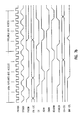
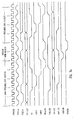
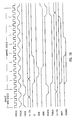
- Figures 7a through 7d are timing diagrams showing the relationship between the various CPU/Bus controller signals for pipelined and non-pipelined I/O bus access and for private memory access.
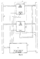
- the functions of the buffer control/byte enable block 37 may be implemented in sections of the address/data buffers 27 as shown in Figure 8 (the address/data buffers 27 may also be implemented as a separate VLSI chip).
- the TTL buffers in the data buffer section 271 are controlled directly by address and byte enable signals which appear on the system main I/O bus 23.
- the data transfer enable bits (BHE and BLE) and the word enable bit utilized to select data addresses (WLE) are generated in the address buffer section 273. This provides for all of the address and byte enable signals to generated on the same chip and to have the same timing.
Abstract
Description
- The present invention relates to microprocessor bus controllers and in particular to bus controllers incorporating state machine technology to provide a functional link between microprocessors having different size data widths, and a data bus which allows access to devices having different size data widths on the data bus.
- In a microprocessor controlled computer system such as a personal or desk top computer, the computer requires a set of electronic connections between the microprocessor and other devices making up the computer system. These communication lines are collectively called the input/output system or I/O bus. All messages in data pass between the microprocessor and other system components travel on the bus. A complete I/O bus includes several component parts: the data bus, lines over which data flows; the address bus, a set of lines that specify the memory addresses to which data will be transferred; and various support lines carrying control signals and power for the various devices on the bus. A bus controller initiates and controls all I/O bus cycles. The controller controls the interface to the I/O bus, the address and data buffers, the CPU, the direct memory access (DMA) device and other memory controllers.
- Prior art bus controllers were integrated into and functioned as a part of the microprocessor architecture. As microprocessor technology has advanced, bus controller technology has become separate and distinct. Similarly, as the number of peripheral devices available for use with various microprocessors has increased, it has become obvious that peripheral devices usable with one integrated microprocessor-bus controller architecture can not generally be used with the bus controller of another microprocessor.
- Separate microprocessor and bus controller architectures provide system design flexibility as well as facilitating interface of many peripheral devices among many different microprocessors. In the present state of the art, microprocessors are expected to interface with memory manage units, CRT controllers, floppy disc controllers, hard disc controllers, arithmetic cove processors and the like. In addition, it is well known that the next generation of 32-byte microprocessors must be able to interface with already existing peripheral devices without the immediate need for specifically designed bus controllers.
- However, even though the present day microprocessor and bus controller architectures are separated, bus controllers designed to interface with a specific type or range of types of microprocessors and peripheral devices are still limited to certain system configurations and further limit design flexibilitas for the next generation of microprocessors. See for example the well-known personal computer models known as the "PC XT" and "PC AT", manufactured and marketed by the IBM Corporation.
- In the past, I/O bus structures and small microprocessor based computer systems comprised little more than buffered extensions of the microprocessor I/O pins. While microprocessors speeds, data widths, architecture and I/O protocols evolve at a rapid rate, system level I/O bus configurations remain essential unchanged in structure and timing for five to ten years. For example, reflecting the capabilities of its 8-bit 8088 microprocessor, the original IBM PC utilizes an I/O bus which permits only eight bits of data to be transferred at one time. With the more advanced PC AT, while maintaining the simplicity in functionality of the original PC I/O bus, IBM added an additional 8 data lines to the I/O bus to provide for 16-bit data transfers. More recently, new more sophisticated I/O buses having greater capabilities have been developed; for example, the IBM "Micro Channel" I/O bus developed for IBM's new "PS/2" computer models. IBM's basic micro-channel design supports 8-bit data transfers with additional pins provided for 16- and 32- bit operations. The biggest advantage of the new micro-channel type I/O buses, is their "multiple master architecture" which allows microprocessors on expansion boards to have full access to the computer system's resources. In order to achieve capabilities and functionality of the new buses, a bus controller is required which automatically accommodates one or more microprocessors, which may have different word or data widths and which allows the microprocessors to access other devices, "slaves", on the bus which may have different data width sizes from each other and from the microprocessors.
- A microprocessor and I/O bus controller according to the principles of the present invention comprises a state machine I/O bus controller which provides a functional control link between the microprocessors and the main I/O data bus. The bus controller provides the signals required to control the data flow to and from the I/O bus. It further generates the control strobes required to facilitate communication between the microprocessors and plug in adapters of 8-,16- or 32-bit widths. While the interface between the microprocessors and the bus controller is synchronous in nature, the 1/0 bus interface may be asynchronous. The microprocessors can have a data width of 16 or 32 bits or more while the devices on the I/O bus can have data widths of 8, 16 or 32 bits. Any difference between the data width size of a microprocessor and the bus device accessed is automatically accommodated by the bus controller state machine. The use of a state machine within a bus controller provides the ability to change the function and timing of various signals quickly and easily, and also provides the means to change the bus cycle functionality and timing (in a dynamic sense) in response to I/O conditions or specific microprocessor access requests. The bus controller also provides reset control and clock generation logic for the computer system.
- In the bus controller of the present invention, the state machine senses and evaluates an access request from a microprocessor; i.e., what kind of processor 16- or 32-bit processor, and which bits have been requested, etc. Then the state machine evaluates the data bus width of the device which is being accessed by the microprocessor request to determine the proper action to be taken. For example, if a 32- bit microprocessor requests 32 bits of data from an 8 bit device, the bus controller accesses that 8-
bit device 4 times in succession, to gather the requested data bits and then passes all 32 bits to the microprocessor simultaneously. Thus, the microprocessor and its controlling application software typically do not have to be aware of data bus widths, because the bus controller automatically accommodates any differences in data widths between the microprocessor and the accessed device. The bus controller includes logic to determine the number of I/0 bus cycles required to satisfy a microprocessor data request to accommodate for the differences in data width sizes between a microprocessor and accessed device. Thus, while the bus controller will generate the 4 byte enable bytes required for any microprocessor access request, if a 16-bit wide microprocessor requests 16 bits of data from a 32-bit wide memory device, the bus controller will only access the memory device once to transfer the two bytes to satisfy the 16-bit data request. - The implementation of the bus controller of the present invention also provides additional features. For example, if a microprocessor needs to access a co-microprocessor, which is physically not on the system main I/O bus, but on the microprocessor board, then the bus controller disables the data buffers to and from the main I/O bus to allow the microprocessor to access the co-microprocessor. Further, the bus controller generates special control signals that disables the I/O bus data buffers and the I/O bus control strobes generated to allow a read access to "private" on board system memory, to allow a much faster access than could be achieved through the system main I/O bus. The bus controller of the present invention can be implemented as a single VLSI component. This allows very efficient use of logic partition and reduction of the total computer system component devices. Furthermore, the system operates faster because of tighter logic integration.
-
- Figure 1 is a block diagram of a typical microprocessor-controlled computer system incorporating an I/O bus and a CPU/Bus controller according to the principals of the present invention;
- Figure 2 is a block diagram of a CPU/Bus controller according to the principles of the present invention;
- Figures 3a, 3b and 3c are a functional block diagram of the CPU/Bus controller shown in figure 2;
- Figures 4a and 4b are a logic diagram of the state machine shown in figures 2 and 3a;
- Figures 5a and 5b are a logic diagram of the last cycle detect circuitry shown in Figures 2 and 3a;
- Figure 6 is a diagram showing the package and pin layout for a VS21 chip implementing the CPU/Bus controller of the present invention;
- Figures 7a-7b are timing diagrams showing the relationship between various signal waveforms in the CPU/Bus controller of Figures 3a-3c; and
- Figure 8 is a conceptual block diagram of an alternate implementation of the bus controller of the present invention.
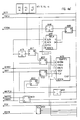
- Referring now to Figure 1, the microprocessor controlled computer system block diagram is shown. The system is controlled by a central processing unit (CPU) 11, such as a 32-bit microprocessor part number 80386, manufactured by Intel Corporation described in the Intel "Microprocessor and Peripheral Handbook", Volume One, Microprocessor, 1988, on pages 4-1 through 4-128, and is incorporated by reference as if fully set forth herein. The
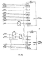
CPU 11 is connected throughbuffers 27 to themain system memory 13 vialocal bus 15 and amemory bus 16. Also connected to thelocal bus 15 is a math co-processor orNPU 17 and a direct memory access (DMA)controller 19. An 80-bit numeric processor extension, part number 80387, manufactured by Intel Corporation, may be used as themath co-processor 17. Themain system memory 13, which can be expanded up to eight megabytes or more of page/interleaved memory, is also coupled to amemory controller 25 and to the address/data buffers 27 viamemory bus 16. TheCPU 11, NPU 17 andDMA controller 19 are also coupled to the address/data buffers 27 and the CPU/Bus controller 21 via thelocal bus 15. To provide access to the remaining components of the computer system, themicroprocessors DMA controller 19 andmain system memory 13 are coupled to the system main I/O bus 23 via the address/data buffers 27. The remaining system components such asfloppy disc controller 29 and others as shown are connected to the system main I/O bus 23. The system main I/O bus 23 is a 32-byte wide "arbitrated" bus similar to the IBM Micro Channel or an Apple Computer, Inc's Nubus. The architecture of this type of I/O bus provides the capability of microprocessors on add-in cards connected to the bus, to act as "master" processors on a par with themain system microprocessor 11 and which may assume temporary control of the entire system. Arbitration circuitry (not shown) included in the I/O bus 23 architecture, allocates microprocessor bus access and assures that no one device can monopolize the I/O bus. The I/O bus 23, provides full support for add-on cards, allowing other devices such as graphic printer controllers, or high resolution graphic display boards to be added to this system. The use of the I/O bus 23 enables access to the devices on the I/O bus 23 and is controlled by the CPU/Bus controller 21. - Referring now, also to Figure 2, a functional block diagram of the CPU/
Bus controller 21 constructed according to the principles of the present invention is shown. The CPU/Bus controller 21 performs the I/O bus control functions for a multiprocessor computer system and acts as the functional control link between themicroprocessors O bus 23. The CPU/Bus controller 21 controls the interface between theCPU 11,NPU 17,DMA controller 19, themain system memory 13, the address/data buffers 27 and thememory controller 25 and the main I/O bus 23. The CPU/Bus controller operations with theCPU 11 are synchronous in nature while the operations with the I/O bus 23 are essential asynchronous. The function link or interface between theCPU 11 and the I/O bus 23 is accomplished by astate machine 31 in the CPU/Bus controller 21. The CPU/Bus controller 21 comprises 8 blocks or sections. These blocks are theclock generator 43, resetcontrol 41, status interpreter 33, byte enable detect 35, last cycle detect 39,state machine 31, access latches 45 and buffer control/byte enable 37. The major signals utilized by the CPU/Bus controller 21 are listed and defined inAppendix 1 attached hereto. - The clock generation section of the CPU/
Bus controller 21 generates clock signals for various other sections of the computer system and comprises thereset control block 41 and theclock generator block 43. Thereset control circuit 41 provides the proper timing and pulse width for a microprocessor reset signal and a system reset signal derived from a raw reset signal. Thereset control circuitry 41 couples the microprocessor reset signal to theclock generator 43 where the processor reset signal is synchronized with the processor clock. Theclock generator 43 generates various clock signals to be used in other functional sections of the computer system; e.g., serial port communications and floppy disk controller functions. The main clock input signal, CLK48M, to theclock generator 43 has a frequency of 48 megaHertz (MHz). This 48 MHz clock signal is frequency divided to provide a peripherals clock, PERCLK, signal having a frequency of 1.846 MHz. The main clock input signal is also divided by 3 to provide a disk clock, DSK16M, signal of 16 MHz which can be used by the floppy disk controller or any other system element requiring a 16 MHz clock. A variable frequency clock, DSK96M, signal is derived from the main clock input signal and has a frequency of 9.6 MHz or 16 MHz depending on the state of the DKCK16 input signal to theclock generator circuit 43. A system clock, SYSCLK, signal is derived from the processor clock, CLKPRO, input to theclock generator 43 and has a frequency equal to one-half the frequency of the processor clock. The system clock is used to synchronize the CPU/Bus controller 21 with themicroprocessor 11 and thememory controller 25. When theCPU 11 comprises a 80386 microprocessor, the processor clock has a frequency of 40 MHz which yields a system clock of 20 MHz. - The status interpreter block 33, the byte enable detect
block 35 and the last cycle detectblock 39 comprise a CPU interface section in the CPU/Bus controller 21. This section responds to an access request from theCPU 11, as indicated for example, by a /ADS signal from themicroprocessor 11 in the case of a 80386 microprocessor. The response can be in the form of a I/O bus access to memory or to a port location. The type of access requested is defined by the signals WRITE, DATA, and MEM/10 in the case of an 80386 microprocessor. This access can be a read or a write and typically takes place through the I/O Bus 23. In addition to normal read/write accesses, the CPU/Bus controller 21 also handles the system cycles for interrupt acknowledge, halt and shutdown. A halt access stops the microprocessor and is not an I/O bus operation in that no data transaction occurs. The shutdown access is also not an I/O bus operation, but in this case the CPU/Bus controller issues a reset signal to the microprocessor. In a normal cycle, the microprocessor concludes the I/O bus access request by sampling a READY signal generated by the CPU/Buscontroller state machine 31 at the completion of an access request. When themicroprocessor 11 detects the presence of the ready signal, the current access cycle will be concluded if the SYSCLK signal is active, and the next access requested may begin. - The status interpreter block 33 interprets status information input from the I/
O bus 23 and microprocessor request information input from theCPU 11 to detect that the microprocessor has requested a bus access or an access to thesystem memory 13. In accordance with Table 1 below, the status interpreter 33 determines what type of access has been requested and provides the proper stimulus signals to thestate machine 31 to commence the proper I/O bus 23 cycle activity.
- In response to information and control signals from the
CPU 11 and the I/O bus 23 the bit enable detectblock 35 evaluates the data bus width of themicroprocessor 11 and the bit enable signal input information in accordance with Table 2 for a 32-bit microprocessor and Table 3 for a 16-bit microprocessor to determine which data bits are being requested by theCPU 11. This information is. then relayed to the I/O bus 23 as well as other sections of the CPU/Bus controller to properly access the requested data. The last cycle detectblock 39 evaluates input information from the I/O bus 23, the byte enable detectblock 35, the CPU/Buscontroller state machine 31 and the data width of the device being accessed to determine if the current I/O bus 23 access cycle is the last access cycle needed to fulfill thecurrent microprocessor 11 request. If the present bus access cycle is the last access cycle required, the CPU/Bus controller 23 generates a ready signal to the microprocessor to allow themicroprocessor 11 to proceed with the next request. The last cycle detectblock 39 also generates the bit enable (i.e., addresses) manipulation control signals for the buffer control/byte enableblock 37.

- The CPU/Bus
controller state machine 31 generates the proper I/O bus 23 control strobes for the I/O bus 23 after the CPU interface section has determined the type of I/O bus cycle requested by a system on board microprocessor such asCPU 11. Thestate machine 31 is a synchronous state machine which supplies the required bus control strobes with appropriate timing. Thestate machine 31 also generates data byte enable signals corresponding to the low order address lines, as well as the actual command strobes and system status signals. Thestate machine 31 also provides cycle status information signals internal to the CPU/Bus controller 21 to indicate which portion of the bus access cycle is currently being executed. In response to internal signals such as the last cycle signal online 38 generated by the last access detectblock 39 and external input signals to the CPU/Bus controller such as I/O ready signals and bus control strobe disable information (utilized in a fast on board memory access), thestate machine 31 also generates the READY signal to themicroprocessor 11. - The buffer control/byte enable
block 37 generates the control signals which control the data path buffers 27 to control the data flow between theCPU 11 and the I/O bus 23. The byte enable (ie., addresses) signals which are necessary for the devices on the I/O bus 23 to properly decode the access are also generated by the buffer control/byte enableblock 37. There are 2 data bytes to be controlled in a 16-bit system and 4 data bytes in a 32-bit system. A portion of the data path comprise crossover buffers which steer data from the lower data word to the upper data word as well as from a lower byte to an upper byte. Three additional buffers can store information on the lower byte for presentation to the microprocessor on subsequent I/O bus commands. This is used when themicroprocessor 11 requests a 16- or 32-bit access to an 8-bit device on the I/O bus 23. In this case, the CPU/Bus controller commands up to 4 I/O bus 23 accesses to satisfy theCPU 11 request. - Each access request from the
microprocessor 11 can generate up to 4 data bytes. In order to satisfy a microprocessor request the CPU/Bus controller may have to access the I/O bus 23 up to 4 times; for example, a 32-bit request to a 8-bit device will require 4 access cycles. - The
microprocessor 11, in the case of a 32-bit microprocessor can request up to 32 bits of data which requires 1 access cycle from a 32-bit device, 2 access cycles from a 16-bit device or 4 access cycles from an 8-bit device. Each block of 8 bits requested requires a data byte enable signal to be generated by the CPU/Bus controller. The number of bus access cycles required is a function of the microprocessor data width, the device data width and the request. When a request is made, the data starting address is provided to the CPU/Bus controller by themicroprocessor 11. If the request is a 4-byte (i.e., 32 bits) request then the access cycle has to start atbyte 0 orbyte 4. A 2-byte request (i.e., 16 bits) can start atbytes byte state machine 31 knows when to commence the access cycles, all it then needs to know is when to stop the access operation; i.e., when the request has been satisfied. The last cycle detectblock 39 determines when the process stops by comparing the current request information from the microprocessor, the accessed device data width size and the data byte address. The highest requested data byte address is compared with the current access cycle and the current data byte enable signal and a READY signal is generated when a match is found. The READY signal indicates to theCPU 11 that the access is complete and the data lines are valid. -
Appendix 2 attached hereto lists the I/O bus access combinations as a function of possible data bytes and access device size.Appendix 3 attached hereto lists the proper byte enable signals corresponding to the different states of the information signals input by the I/O bus 23 and theCPU 11. Appendix IV attached hereto lists the conditions under which the last cycle detectblock 39 generates a LAST CYCLE signal to thestate machine 31 online 38. - The preferred embodiment of the CPU/
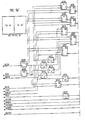
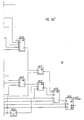
Bus controller 21 is implemented in one VLSI chip integrated circuit housed in a rectangular 68-pin package. Figures 3a, 3b, and 3c are a functional logic block diagram of the VLSI integrated circuit which implements CPU/Bus controller 21. Figures 4a and 4b are a detailed logic diagram of the CPU/Buscontroller state machine 31 and Figures 5a and 5b are a detailed logic diagram of the last cycle detectblock 39. The package layout and pin assignments are shown in Figure 6. Appendix V attached hereto lists the electrical specifications for the VLS1 chip package. Figures 7a through 7d are timing diagrams showing the relationship between the various CPU/Bus controller signals for pipelined and non-pipelined I/O bus access and for private memory access. - Alternatively, the functions of the buffer control/byte enable
block 37 may be implemented in sections of the address/data buffers 27 as shown in Figure 8 (the address/data buffers 27 may also be implemented as a separate VLSI chip). In this embodiment, the TTL buffers in thedata buffer section 271 are controlled directly by address and byte enable signals which appear on the system main I/O bus 23. The data transfer enable bits (BHE and BLE) and the word enable bit utilized to select data addresses (WLE) are generated in theaddress buffer section 273. This provides for all of the address and byte enable signals to generated on the same chip and to have the same timing. - While the present invention has been described in conjunction with a specific embodiment thereof, it will be understood by those skilled in the art that alternatives, modifications and variations in form and detail may be made without departing from the spirit of the invention or exceeding the scope of the appended claims.
Claims (22)


Applications Claiming Priority (2)
| Application Number | Priority Date | Filing Date | Title |
|---|---|---|---|
| US419096 | 1989-10-11 | ||
| US07/419,096 US5220651A (en) | 1989-10-11 | 1989-10-11 | Cpu-bus controller for accomplishing transfer operations between a controller and devices coupled to an input/output bus |
Publications (3)
| Publication Number | Publication Date |
|---|---|
| EP0423036A2 true EP0423036A2 (en) | 1991-04-17 |
| EP0423036A3 EP0423036A3 (en) | 1991-09-25 |
| EP0423036B1 EP0423036B1 (en) | 1998-11-25 |
Family
ID=23660769
Family Applications (1)
| Application Number | Title | Priority Date | Filing Date |
|---|---|---|---|
| EP90402847A Expired - Lifetime EP0423036B1 (en) | 1989-10-11 | 1990-10-11 | CPU-bus controller |
Country Status (7)
| Country | Link |
|---|---|
| US (1) | US5220651A (en) |
| EP (1) | EP0423036B1 (en) |
| JP (1) | JP3302357B2 (en) |
| KR (1) | KR0156922B1 (en) |
| CA (1) | CA2026068A1 (en) |
| DE (1) | DE69032783T2 (en) |
| SG (1) | SG43847A1 (en) |
Cited By (3)
| Publication number | Priority date | Publication date | Assignee | Title |
|---|---|---|---|---|
| WO1994016388A1 (en) * | 1992-12-31 | 1994-07-21 | Seiko Epson Corporation | System and method for controlling the input and output of data between a host processor and an i/o device |
| US5682508A (en) * | 1995-03-23 | 1997-10-28 | Onset Computer Corporation | UART protocol that provides predictable delay for communication between computers of disparate ability |
| EP0817090A2 (en) * | 1996-07-01 | 1998-01-07 | Sun Microsystems, Inc. | System for multisized bus coupling in a packet-switched computer system |
Families Citing this family (29)
| Publication number | Priority date | Publication date | Assignee | Title |
|---|---|---|---|---|
| US5537602A (en) * | 1988-09-16 | 1996-07-16 | Hitachi, Ltd. | Process system for controlling bus system to communicate data between resource and processor |
| JP2511146B2 (en) * | 1989-07-07 | 1996-06-26 | 富士通株式会社 | Data processing device |
| JP2776390B2 (en) * | 1989-11-30 | 1998-07-16 | 富士通株式会社 | Transmission and reception bus interface |
| US5333294A (en) * | 1990-10-09 | 1994-07-26 | Compaq Computer Corporation | Configurable data width direct memory access device with a read address counter and a write address counter which increments the addresses based on the desired data transfer width |
| US5353417A (en) * | 1991-05-28 | 1994-10-04 | International Business Machines Corp. | Personal computer with bus interface controller coupled directly with local processor and input/output data buses and for anticipating memory control changes on arbitration for bus access |
| US5418930A (en) * | 1991-09-05 | 1995-05-23 | International Business Machines Corporation | Circuit for interfacing asynchronous to synchronous communications |
| US5511229A (en) * | 1991-09-13 | 1996-04-23 | Matsushita Electric Industrial Co., Ltd. | Data processing system having a switching network connecting multiple peripheral devices using data paths capable of different data bus widths |
| US5341495A (en) * | 1991-10-04 | 1994-08-23 | Bull Hn Information Systems, Inc. | Bus controller having state machine for translating commands and controlling accesses from system bus to synchronous bus having different bus protocols |
| US5341508A (en) * | 1991-10-04 | 1994-08-23 | Bull Hn Information Systems Inc. | Processing unit having multiple synchronous bus for sharing access and regulating system bus access to synchronous bus |
| JPH0619466A (en) * | 1992-07-01 | 1994-01-28 | Kawai Musical Instr Mfg Co Ltd | Music information processing system |
| US5469547A (en) * | 1992-07-17 | 1995-11-21 | Digital Equipment Corporation | Asynchronous bus interface for generating individual handshake signal for each data transfer based on associated propagation delay within a transaction |
| US5745791A (en) * | 1992-09-16 | 1998-04-28 | Intel Corporation | System for interfacing first and second components having different data path width by generating first and second component address to read data into buffer |
| US5299315A (en) * | 1992-09-17 | 1994-03-29 | International Business Machines Corp. | Personal computer with programmable threshold FIFO registers for data transfer |
| TW276312B (en) * | 1992-10-20 | 1996-05-21 | Cirrlis Logic Inc | |
| JP3369227B2 (en) * | 1992-11-09 | 2003-01-20 | 株式会社東芝 | Processor |
| US5649162A (en) * | 1993-05-24 | 1997-07-15 | Micron Electronics, Inc. | Local bus interface |
| US5513372A (en) * | 1993-08-23 | 1996-04-30 | Intel Corporation | Peripheral interface having hold control logic for generating stall signals to arbitrate two read and one write operations between processor and peripheral |
| US5426740A (en) * | 1994-01-14 | 1995-06-20 | Ast Research, Inc. | Signaling protocol for concurrent bus access in a multiprocessor system |
| US5678064A (en) * | 1994-12-01 | 1997-10-14 | International Business Machines Corporation | Local bus-ISA bridge for supporting PIO and third party DMA data transfers to IDE drives |
| US5867672A (en) * | 1996-05-21 | 1999-02-02 | Integrated Device Technology, Inc. | Triple-bus FIFO buffers that can be chained together to increase buffer depth |
| US6230216B1 (en) * | 1999-01-28 | 2001-05-08 | Vlsi Technology, Inc. | Method for eliminating dual address cycles in a peripheral component interconnect environment |
| JP3886870B2 (en) * | 2002-09-06 | 2007-02-28 | 株式会社ルネサステクノロジ | Data processing device |
| JP4542308B2 (en) * | 2002-12-16 | 2010-09-15 | 株式会社ソニー・コンピュータエンタテインメント | Signal processing device and information processing device |
| EP1619588B1 (en) * | 2004-07-21 | 2007-05-09 | STMicroelectronics Limited | Memory access |
| US20070073932A1 (en) * | 2005-09-13 | 2007-03-29 | Alcatel | Method and apparatus for a configurable data path interface |
| US8667254B1 (en) * | 2008-05-15 | 2014-03-04 | Xilinx, Inc. | Method and apparatus for processing data in an embedded system |
| CN103198043B (en) * | 2013-01-24 | 2016-05-11 | 杭州中科微电子有限公司 | A kind of improved AHB to APB bus bridge and control method thereof |
| US9543044B2 (en) * | 2013-11-07 | 2017-01-10 | Stmicroelectronics International N.V. | System and method for improving memory performance and identifying weak bits |
| KR200483746Y1 (en) | 2015-07-24 | 2017-07-03 | 퍼니피쉬(주) | Lamp |
Citations (4)
| Publication number | Priority date | Publication date | Assignee | Title |
|---|---|---|---|---|
| US4315308A (en) * | 1978-12-21 | 1982-02-09 | Intel Corporation | Interface between a microprocessor chip and peripheral subsystems |
| WO1986000436A1 (en) * | 1984-06-26 | 1986-01-16 | Motorola, Inc. | Data processor having dynamic bus sizing |
| US4580213A (en) * | 1982-07-07 | 1986-04-01 | Motorola, Inc. | Microprocessor capable of automatically performing multiple bus cycles |
| EP0333319A2 (en) * | 1988-03-14 | 1989-09-20 | Advanced Micro Devices, Inc. | Bus-combatible programmable sequencers |
Family Cites Families (19)
| Publication number | Priority date | Publication date | Assignee | Title |
|---|---|---|---|---|
| US3969722A (en) * | 1974-07-03 | 1976-07-13 | General Electric Company | Method and apparatus for operator interrogation of simulated control circuits |
| US4124889A (en) * | 1975-12-24 | 1978-11-07 | Computer Automation, Inc. | Distributed input/output controller system |
| JPS5427741A (en) * | 1977-08-03 | 1979-03-02 | Toshiba Corp | Information processing organization |
| GB1601955A (en) * | 1977-10-21 | 1981-11-04 | Marconi Co Ltd | Data processing systems |
| US4363094A (en) * | 1977-12-29 | 1982-12-07 | M/A-COM DDC, Inc. | Communications processor |
| US4268904A (en) * | 1978-02-15 | 1981-05-19 | Tokyo Shibaura Electric Co., Ltd. | Interruption control method for multiprocessor system |
| US4400778A (en) * | 1979-11-05 | 1983-08-23 | Litton Resources Systems, Inc. | Large-volume, high-speed data processor |
| US4491916A (en) * | 1979-11-05 | 1985-01-01 | Litton Resources Systems, Inc. | Large volume, high speed data processor |
| JPS5789128A (en) * | 1980-11-25 | 1982-06-03 | Hitachi Ltd | Controlling system for information interchange |
| US4562533A (en) * | 1981-12-03 | 1985-12-31 | Ncr Corporation | Data communications system to system adapter |
| US4476527A (en) * | 1981-12-10 | 1984-10-09 | Data General Corporation | Synchronous data bus with automatically variable data rate |
| US4602327A (en) * | 1983-07-28 | 1986-07-22 | Motorola, Inc. | Bus master capable of relinquishing bus on request and retrying bus cycle |
| US4835681A (en) * | 1984-06-27 | 1989-05-30 | Compaq Computer Corporation | Personal computer having normal and high speed execution modes |
| US4727491A (en) * | 1984-06-27 | 1988-02-23 | Compaq Computer Corporation | Personal computer having normal and high speed execution modes |
| BG39765A1 (en) * | 1985-02-14 | 1986-08-15 | Turlakov | Device for connecting 8- degree and 16- degree modules to 16- degree microprocessor system |
| EP0256267B1 (en) * | 1986-08-12 | 1994-03-02 | Hitachi, Ltd. | Microprocessor for retrying data transfer |
| US4787032A (en) * | 1986-09-08 | 1988-11-22 | Compaq Computer Corporation | Priority arbitration circuit for processor access |
| GB2196762B (en) * | 1986-10-27 | 1990-12-19 | Burr Brown Ltd | Interleaved access to global memory by high priority source |
| US4987529A (en) * | 1988-08-11 | 1991-01-22 | Ast Research, Inc. | Shared memory bus system for arbitrating access control among contending memory refresh circuits, peripheral controllers, and bus masters |
-
1989
- 1989-10-11 US US07/419,096 patent/US5220651A/en not_active Expired - Lifetime
-
1990
- 1990-09-24 CA CA002026068A patent/CA2026068A1/en not_active Abandoned
- 1990-10-11 DE DE69032783T patent/DE69032783T2/en not_active Expired - Lifetime
- 1990-10-11 KR KR1019900016189A patent/KR0156922B1/en not_active IP Right Cessation
- 1990-10-11 SG SG1996002138A patent/SG43847A1/en unknown
- 1990-10-11 JP JP27514790A patent/JP3302357B2/en not_active Expired - Lifetime
- 1990-10-11 EP EP90402847A patent/EP0423036B1/en not_active Expired - Lifetime
Patent Citations (4)
| Publication number | Priority date | Publication date | Assignee | Title |
|---|---|---|---|---|
| US4315308A (en) * | 1978-12-21 | 1982-02-09 | Intel Corporation | Interface between a microprocessor chip and peripheral subsystems |
| US4580213A (en) * | 1982-07-07 | 1986-04-01 | Motorola, Inc. | Microprocessor capable of automatically performing multiple bus cycles |
| WO1986000436A1 (en) * | 1984-06-26 | 1986-01-16 | Motorola, Inc. | Data processor having dynamic bus sizing |
| EP0333319A2 (en) * | 1988-03-14 | 1989-09-20 | Advanced Micro Devices, Inc. | Bus-combatible programmable sequencers |
Cited By (5)
| Publication number | Priority date | Publication date | Assignee | Title |
|---|---|---|---|---|
| WO1994016388A1 (en) * | 1992-12-31 | 1994-07-21 | Seiko Epson Corporation | System and method for controlling the input and output of data between a host processor and an i/o device |
| US5499384A (en) * | 1992-12-31 | 1996-03-12 | Seiko Epson Corporation | Input output control unit having dedicated paths for controlling the input and output of data between host processor and external device |
| US5682508A (en) * | 1995-03-23 | 1997-10-28 | Onset Computer Corporation | UART protocol that provides predictable delay for communication between computers of disparate ability |
| EP0817090A2 (en) * | 1996-07-01 | 1998-01-07 | Sun Microsystems, Inc. | System for multisized bus coupling in a packet-switched computer system |
| EP0817090A3 (en) * | 1996-07-01 | 2004-01-28 | Sun Microsystems, Inc. | System for multisized bus coupling in a packet-switched computer system |
Also Published As
| Publication number | Publication date |
|---|---|
| US5220651A (en) | 1993-06-15 |
| EP0423036B1 (en) | 1998-11-25 |
| SG43847A1 (en) | 1997-11-14 |
| KR0156922B1 (en) | 1998-11-16 |
| JPH03208153A (en) | 1991-09-11 |
| JP3302357B2 (en) | 2002-07-15 |
| CA2026068A1 (en) | 1991-04-12 |
| DE69032783D1 (en) | 1999-01-07 |
| KR910008589A (en) | 1991-05-31 |
| DE69032783T2 (en) | 1999-07-01 |
| EP0423036A3 (en) | 1991-09-25 |
Similar Documents
| Publication | Publication Date | Title |
|---|---|---|
| US5220651A (en) | Cpu-bus controller for accomplishing transfer operations between a controller and devices coupled to an input/output bus | |
| JP2571673B2 (en) | Method and apparatus for providing back-to-back data transfer in an information processing system having a multiplexed bus | |
| US5191657A (en) | Microcomputer architecture utilizing an asynchronous bus between microprocessor and industry standard synchronous bus | |
| JP2573566B2 (en) | Bus converter | |
| US5867675A (en) | Apparatus and method for combining data streams with programmable wait states | |
| US5440751A (en) | Burst data transfer to single cycle data transfer conversion and strobe signal conversion | |
| US5937173A (en) | Dual purpose computer bridge interface for accelerated graphics port or registered peripheral component interconnect devices | |
| US6557068B2 (en) | High speed peripheral interconnect apparatus, method and system | |
| US5819096A (en) | PCI to ISA interrupt protocol converter and selection mechanism | |
| US6185520B1 (en) | Method and system for bus switching data transfers | |
| US7523245B1 (en) | Compact ISA-bus interface | |
| US5774681A (en) | Method and apparatus for controlling a response timing of a target ready signal on a PCI bridge | |
| JPH1173386A (en) | Computer system provided with peripheral element connection bus | |
| US5561772A (en) | Expansion bus system for replicating an internal bus as an external bus with logical interrupts replacing physical interrupt lines | |
| US5748945A (en) | Method for slave DMA emulation on a computer system bus | |
| EP0795157A1 (en) | Bridge between two buses | |
| US6247088B1 (en) | Bridgeless embedded PCI computer system using syncronous dynamic ram architecture | |
| US5951667A (en) | Method and apparatus for connecting expansion buses to a peripheral component interconnect bus | |
| US5721882A (en) | Method and apparatus for interfacing memory devices operating at different speeds to a computer system bus | |
| US5689660A (en) | Enhanced peripheral component interconnect bus protocol | |
| US6021483A (en) | PCI-to-PCI bridges with a timer register for storing a delayed transaction latency | |
| US5978869A (en) | Enhanced dual speed bus computer system | |
| US6490638B1 (en) | General purpose bus with programmable timing | |
| JPH10198629A (en) | Method and device for transaction communication between two pct buses | |
| US6067590A (en) | Data bus agent including a storage medium between a data bus and the bus agent device |
Legal Events
| Date | Code | Title | Description |
|---|---|---|---|
| PUAI | Public reference made under article 153(3) epc to a published international application that has entered the european phase |
Free format text: ORIGINAL CODE: 0009012 |
|
| AK | Designated contracting states |
Kind code of ref document: A2 Designated state(s): BE CH DE DK ES FR GB IT LI NL SE |
|
| PUAL | Search report despatched |
Free format text: ORIGINAL CODE: 0009013 |
|
| AK | Designated contracting states |
Kind code of ref document: A3 Designated state(s): BE CH DE DK ES FR GB IT LI NL SE |
|
| 17P | Request for examination filed |
Effective date: 19920311 |
|
| RAP1 | Party data changed (applicant data changed or rights of an application transferred) |
Owner name: MICRAL, INC. |
|
| 17Q | First examination report despatched |
Effective date: 19950913 |
|
| RAP1 | Party data changed (applicant data changed or rights of an application transferred) |
Owner name: AST RESEARCH, INC. |
|
| GRAG | Despatch of communication of intention to grant |
Free format text: ORIGINAL CODE: EPIDOS AGRA |
|
| GRAG | Despatch of communication of intention to grant |
Free format text: ORIGINAL CODE: EPIDOS AGRA |
|
| GRAH | Despatch of communication of intention to grant a patent |
Free format text: ORIGINAL CODE: EPIDOS IGRA |
|
| GRAH | Despatch of communication of intention to grant a patent |
Free format text: ORIGINAL CODE: EPIDOS IGRA |
|
| GRAA | (expected) grant |
Free format text: ORIGINAL CODE: 0009210 |
|
| AK | Designated contracting states |
Kind code of ref document: B1 Designated state(s): BE CH DE DK ES FR GB IT LI NL SE |
|
| PG25 | Lapsed in a contracting state [announced via postgrant information from national office to epo] |
Ref country code: IT Free format text: LAPSE BECAUSE OF FAILURE TO SUBMIT A TRANSLATION OF THE DESCRIPTION OR TO PAY THE FEE WITHIN THE PRE;WARNING: LAPSES OF ITALIAN PATENTS WITH EFFECTIVE DATE BEFORE 2007 MAY HAVE OCCURRED AT ANY TIME BEFORE 2007. THE CORRECT EFFECTIVE DATE MAY BE DIFFERENT FROM THE ONE RECORDED.SCRIBED TIME-LIMIT Effective date: 19981125 Ref country code: FR Free format text: LAPSE BECAUSE OF FAILURE TO SUBMIT A TRANSLATION OF THE DESCRIPTION OR TO PAY THE FEE WITHIN THE PRESCRIBED TIME-LIMIT Effective date: 19981125 Ref country code: ES Free format text: THE PATENT HAS BEEN ANNULLED BY A DECISION OF A NATIONAL AUTHORITY Effective date: 19981125 Ref country code: NL Free format text: LAPSE BECAUSE OF FAILURE TO SUBMIT A TRANSLATION OF THE DESCRIPTION OR TO PAY THE FEE WITHIN THE PRESCRIBED TIME-LIMIT Effective date: 19981125 Ref country code: CH Free format text: LAPSE BECAUSE OF FAILURE TO SUBMIT A TRANSLATION OF THE DESCRIPTION OR TO PAY THE FEE WITHIN THE PRESCRIBED TIME-LIMIT Effective date: 19981125 Ref country code: BE Free format text: LAPSE BECAUSE OF FAILURE TO SUBMIT A TRANSLATION OF THE DESCRIPTION OR TO PAY THE FEE WITHIN THE PRESCRIBED TIME-LIMIT Effective date: 19981125 Ref country code: LI Free format text: LAPSE BECAUSE OF FAILURE TO SUBMIT A TRANSLATION OF THE DESCRIPTION OR TO PAY THE FEE WITHIN THE PRESCRIBED TIME-LIMIT Effective date: 19981125 Ref country code: SE Free format text: THE PATENT HAS BEEN ANNULLED BY A DECISION OF A NATIONAL AUTHORITY Effective date: 19981125 |
|
| REG | Reference to a national code |
Ref country code: CH Ref legal event code: EP |
|
| REF | Corresponds to: |
Ref document number: 69032783 Country of ref document: DE Date of ref document: 19990107 |
|
| PG25 | Lapsed in a contracting state [announced via postgrant information from national office to epo] |
Ref country code: DK Free format text: LAPSE BECAUSE OF FAILURE TO SUBMIT A TRANSLATION OF THE DESCRIPTION OR TO PAY THE FEE WITHIN THE PRESCRIBED TIME-LIMIT Effective date: 19990225 |
|
| EN | Fr: translation not filed | ||
| NLV1 | Nl: lapsed or annulled due to failure to fulfill the requirements of art. 29p and 29m of the patents act | ||
| REG | Reference to a national code |
Ref country code: CH Ref legal event code: PL |
|
| PLBE | No opposition filed within time limit |
Free format text: ORIGINAL CODE: 0009261 |
|
| STAA | Information on the status of an ep patent application or granted ep patent |
Free format text: STATUS: NO OPPOSITION FILED WITHIN TIME LIMIT |
|
| 26N | No opposition filed | ||
| REG | Reference to a national code |
Ref country code: GB Ref legal event code: IF02 |
|
| REG | Reference to a national code |
Ref country code: GB Ref legal event code: 732E |
|
| REG | Reference to a national code |
Ref country code: GB Ref legal event code: 732E |
|
| PGFP | Annual fee paid to national office [announced via postgrant information from national office to epo] |
Ref country code: GB Payment date: 20090914 Year of fee payment: 20 |
|
| PGFP | Annual fee paid to national office [announced via postgrant information from national office to epo] |
Ref country code: DE Payment date: 20091030 Year of fee payment: 20 |
|
| REG | Reference to a national code |
Ref country code: GB Ref legal event code: PE20 Expiry date: 20101010 |
|
| PG25 | Lapsed in a contracting state [announced via postgrant information from national office to epo] |
Ref country code: GB Free format text: LAPSE BECAUSE OF EXPIRATION OF PROTECTION Effective date: 20101010 |
|
| PG25 | Lapsed in a contracting state [announced via postgrant information from national office to epo] |
Ref country code: DE Free format text: LAPSE BECAUSE OF EXPIRATION OF PROTECTION Effective date: 20101011 |