EP0413363A2 - Circuit for generating data of a letter to be displayed on a screen - Google Patents
Circuit for generating data of a letter to be displayed on a screen Download PDFInfo
- Publication number
- EP0413363A2 EP0413363A2 EP90115834A EP90115834A EP0413363A2 EP 0413363 A2 EP0413363 A2 EP 0413363A2 EP 90115834 A EP90115834 A EP 90115834A EP 90115834 A EP90115834 A EP 90115834A EP 0413363 A2 EP0413363 A2 EP 0413363A2
- Authority
- EP
- European Patent Office
- Prior art keywords
- letter
- data
- color
- displayed
- memory
- Prior art date
- Legal status (The legal status is an assumption and is not a legal conclusion. Google has not performed a legal analysis and makes no representation as to the accuracy of the status listed.)
- Withdrawn
Links
Images


Classifications
-
- G—PHYSICS
- G09—EDUCATION; CRYPTOGRAPHY; DISPLAY; ADVERTISING; SEALS
- G09G—ARRANGEMENTS OR CIRCUITS FOR CONTROL OF INDICATING DEVICES USING STATIC MEANS TO PRESENT VARIABLE INFORMATION
- G09G5/00—Control arrangements or circuits for visual indicators common to cathode-ray tube indicators and other visual indicators
- G09G5/22—Control arrangements or circuits for visual indicators common to cathode-ray tube indicators and other visual indicators characterised by the display of characters or indicia using display control signals derived from coded signals representing the characters or indicia, e.g. with a character-code memory
- G09G5/24—Generation of individual character patterns
-
- H—ELECTRICITY
- H01—ELECTRIC ELEMENTS
- H01H—ELECTRIC SWITCHES; RELAYS; SELECTORS; EMERGENCY PROTECTIVE DEVICES
- H01H2219/00—Legends
- H01H2219/054—Optical elements
- H01H2219/064—Optical isolation of switch sites
-
- H—ELECTRICITY
- H01—ELECTRIC ELEMENTS
- H01H—ELECTRIC SWITCHES; RELAYS; SELECTORS; EMERGENCY PROTECTIVE DEVICES
- H01H2231/00—Applications
- H01H2231/022—Telephone handset
Definitions
- This invention relates to a circuit for generating data of a letter to be displayed on a screen, and more particularly to, a circuit for generating data of a letter to be displayed on a screen, and color-data of the letter and a background to be displayed along with the letter.
- a circuit for generating data of a letter to be displayed on a screen is widely used to display a number, a symbol, an alphabetical letter, etc. (simply defined "letter” hereinafter) which are superimposed on a video image displayed on a CRT screen of a raster scan type.
- a typical example of the letter is a channel number, etc. displayed on a video image which has been displayed on a CRT screen of a television set.
- a conventional circuit for generating data of a letter comprises a character memory for storing data of letters to be displayed, and a video memory for temporarily storing an address of the character memory to be accessed
- a predetermined address information is written into the video memory to access the character memory, so that data of a letter to be displayed is read from the character memory by the address information.
- the data of the letter read from the character memory is supplied to a display circuit including a CRT screen, so that at least one letter is displayed at a predetermined position on the CRT screen by superimposing the data of the letter on data of a video image at a predetermined timing, or by replacing a portion of the video image data with the letter data.
- a disadvantage occurs in that a storing capacity of a memory is increased to result in the increase of a chip area of an integrated circuit for this circuit for generating data of a letter.
- a occupied area of the memory is increased, other parts are limited to be included in, for instance, a television set, so that other functions are limited to be added thereto. This disadvantage becomes remarkable, as the number of letters to be stored is increased.
- a circuit for generating data of a letter to be displayed on a screen comprises a first memory for storing data of plural letters each including a letter portion and a background portion, means for reading data of at least one letter to be displayed from the first memory, a second memory for temporarily storing color data for a portion selected from the letter portion and the background portion of the at least one letter, and means connected to the first and second memories for generating a letter color signal indicative of a predetermined color in response to the letter portion of the at least one letter and the color data, and a background color signal indicative of a color different from the predetermined color in response to the background portion of the at least one letter and the color data.
- the letter portion and the background portion have different information from each other among data of the plural letters stored in the first memory, and the color data are used common to the letter portion and the background portion to generate different color signals for the letter and background portions.
- a letter color and a background color have a relation of complementary colors.
- Color data are of, for instance, three bit signals corresponding to red, blue, and green to designate eight colors.
- the color data is used to determine a color of the letter portion, when the letter portion is read from a memory. Otherwise, a complementary color relative to the color of the letter portion is used for a color of the background portion.
- the complementary color is based on data which is obtained by inverting all bits of the color data of the letter portion Consequently, the contrast between a letter and a background displayed on a screen is made clear.
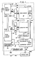
- Fig. 1 shows a circuit for generating data of a letter to be displayed on a screen in the preferred embodiment according to this invention.
- This circuit 100 has a character ROM 50 for storing data corresponding to plural letters which can be displayed on a CRT screen of a display unit 200. Among the plural letters, at least one letter is selected to be displayed by command data supplied through a command bus 11 from an external controller (not shown).
- the command data include information of a letter to be displayed and information designating a color of the letter, and are transferred to a write control circuit 10.
- start address information of a memory region of the character ROM 50 storing a letter to be displayed and color data corresponding to the letter are generated, and supplied through a data bus 12 to a RAM (Random Access Memory) 20.
- an address of the RAM 20 is designated by address information supplied through a write address bus 13, a multiplexer 30, and an access address bus 31 from the write control circuit 10.
- the RAM 20 includes a VRAM (Video RAM) region 21, to which the start address information is written, and a color data memory region 22, to which the color data are written.
- the write control circuit 10 is supplied with a horizontal synchronous pulse Hs and a vertical synchronous pulse Vs from the display unit 200, and controls the RAM 20 to store data of following display in place of formerly stored data during horizontal and/or vertical retrace periods. Thus, a letter and a color to be displayed are designated.
- the RAM 20 is also controlled by a read control circuit 70, so that data are read from the RAM 20.
- the read control circuit 70 provides a predetermined timing signal in accordance with the horizontal and vertical synchronous pulses Hs and Vs, and a clock signal St generated to be synchronous with the horizontal synchronous pulse Hs by a synchronous oscillator 80.
- the RAM 20 is accessed by address information supplied through a read address bus 71, the multiplexer 30, and the access address bus 31 from the read control circuit 70.
- the start address information is read at an accessed address from the VRAM region 21, while the color data are read at an accessed address from the color data region 22.
- the start address information thus read from the VRAM region 21 is supplied through a data bus 23 to an upper bit region 41 of a ROM pointer 40, and is latched therein.
- the VRAM region 21 has a width of eight bits, and the character ROM 50 has addresses each having twelve bits.
- a lower bit region 42 of the ROM pointer 40 is of four bits which are incremented by receiving the horizontal synchronous pulse Hs.
- Address information is supplied from the ROM pointer 40 to the character ROM 50, from which data corresponding to one horizontal scanning period among data of a letter to be displayed are read in parallel.
- each of letters stored in the character ROM 50 has a width of seven bits and a height of nine bits. This means that data of seven bits are read from the character ROM 50 to be supplied through a data bus 51 to a shift register 60, in which the seven bit data are latched to be supplied to a line 61 one bit by one bit synchronously with a shift clock signal.
- the lower bit region 42 is reset by a reset signal supplied from the read control circuit 70.
- the read control circuit 70 supplies the display unit 200 with a blanking signal BLK on a signal line 72 to communicate the conduct of displaying a letter on the CRT screen thereto.
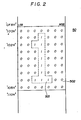
- Fig. 2 shows a memory map addressed from "100H” (H: hexadecinormal digit) to "108H” in the character ROM 50.
- This memory region is a region having a size of seven bits by nine bits as explained before to define a letter portion 501 and a background portion 502.
- data having ten bits of "1” are stored in the letter portion 501, while data having the remaining bits of "0" are stored in the background portion 502.
- data of the other letters are stored in other regions of the character ROM 50.
- address information supplied from the ROM pointer 40 is "102H”
- data of "0011000" are read from the character ROM 50 to be latched in the shift register 60.
- Output data SCD on a signal line 61 of the shift register 60 are supplied to a letter color/background color signal generating circuit 90 together with the color data 5cc read from the color data region 22 of the VRAM 20, so that a letter display/color data signal SD having different information between the letter and background portions for a letter to be displayed is generated therein to be supplied through a signal line 91 to the display unit 200.
- a portion of a video image signal is replaced with the letter display/color data signal SD by the blanking signal BLK, so that at least one letter having a predetermined color and a background having a complementary color relative to the predetermined color are displayed at a predetermined position on the CRT screen of the display unit 200.
- the letter color/background color signal generating circuit 90 is controlled as to whether or not the background should have a color by a control signal C, and controlled in timing of supplying the letter display/color data signal SD to the display unit 200 by the clock signal St supplied from the synchronous oscillator 80.
- Fig. 3 shows the letter color/background color signal generating circuit 90 comprising an inverter 901, a NAND gate 902, an OR gate 903, three Exclusive-NOR gates 904 to 906, three AND gates 907 to 909, and three D-flip flops 910 to 912 which are connected to each other as shown therein.
- the color data Scc are of three bits corresponding to red SccR, green SccG, and blue SccB, respectively.
- output data SD supplied to the display unit 200 are of three bits corresponding to red SDR, green SDG, and blue SDB, respectively, so that eight kinds of colors can be designated.
- the data are supplied from the shift register 60 via the signal line 61 to the letter color/background color generating circuit 90 one bit by one bit in the order of LSB to MSB as the signal SCD synchronously with the shift clock signal SCK.
- the shift output SCD having a waveform as shown in Fig. 4A is obtained.
- a color of a letter to be displayed, and a color of a background which is a complementary color of the letter color can be displayed on the CRT display only by color data Scc designating the letter color.
- a letter can be displayed by a color different from those of other letters, and a background can be also displayed by a color different from that of the displayed letter and those of other backgrounds.
- the control signal C is "0", so that the output of the NAND gate 902 is fixed to be "1". Therefore, only when data of the letter portion 501 are supplied from the circuit 90 to the display unit 200, the output data SD for a color designated by the color data Scc are generated therein. On the other hand, each bit of the output data SD is "0", when data of the background portion 502 are supplied from the circuit 90 to the display unit 200.
- a color of a letter to be displayed is designated by color data Scc
- a color of a background corresponding to the letter may thereby be designated.
- the inverter 901 is connected to the OR gate 903 instead of the NAND gate 902.
- the bit number of color data, letter data, etc. may be changed.
Landscapes
- Engineering & Computer Science (AREA)
- Physics & Mathematics (AREA)
- Computer Hardware Design (AREA)
- General Physics & Mathematics (AREA)
- Theoretical Computer Science (AREA)
- Controls And Circuits For Display Device (AREA)
- Studio Circuits (AREA)
Abstract
A letter having a letter portion and a background portion is displayed on a screen. One of the letter portion and the background portion is displayed with a first color designated by color data stored in a memory, and the remaining one thereof is displayed with a second color which is determined by data obtained by inverting data of the first color.
Description
- This invention relates to a circuit for generating data of a letter to be displayed on a screen, and more particularly to, a circuit for generating data of a letter to be displayed on a screen, and color-data of the letter and a background to be displayed along with the letter.
- A circuit for generating data of a letter to be displayed on a screen is widely used to display a number, a symbol, an alphabetical letter, etc. (simply defined "letter" hereinafter) which are superimposed on a video image displayed on a CRT screen of a raster scan type. A typical example of the letter is a channel number, etc. displayed on a video image which has been displayed on a CRT screen of a television set.
- A conventional circuit for generating data of a letter comprises a character memory for storing data of letters to be displayed, and a video memory for temporarily storing an address of the character memory to be accessed In this circuit, a predetermined address information is written into the video memory to access the character memory, so that data of a letter to be displayed is read from the character memory by the address information. The data of the letter read from the character memory is supplied to a display circuit including a CRT screen, so that at least one letter is displayed at a predetermined position on the CRT screen by superimposing the data of the letter on data of a video image at a predetermined timing, or by replacing a portion of the video image data with the letter data.
- In such a circuit for generating data of a letter, it is required in recent years that a letter selected from plural letters is displayed by a predetermined color which is different those of the remaining letters. It is also required that a background of the displayed letter selected from plural backgrounds is displayed by a predetermined color which is different from that of the displayed letter, and from those of the remaining backgrounds. For this purpose, it is necessary that a memory for storing data designating a color of a letter to be displayed and data designating a color of a background corresponding to the letter is provided.
- However, where such a memory is provided to realize the above explained purpose, a disadvantage occurs in that a storing capacity of a memory is increased to result in the increase of a chip area of an integrated circuit for this circuit for generating data of a letter. As an occupied area of the memory is increased, other parts are limited to be included in, for instance, a television set, so that other functions are limited to be added thereto. This disadvantage becomes remarkable, as the number of letters to be stored is increased.
- Accordingly, it is an object of this invention to provide an improved circuit for generating data of a letter to be displayed on a screen.
- It is a further object of this invention to provide a circuit for generating data of a letter to be displayed on a screen, in which data for a color of a letter to be displayed, and for a color of a background corresponding to the letter are generated.
- According to this invention, a circuit for generating data of a letter to be displayed on a screen comprises a first memory for storing data of plural letters each including a letter portion and a background portion, means for reading data of at least one letter to be displayed from the first memory, a second memory for temporarily storing color data for a portion selected from the letter portion and the background portion of the at least one letter, and means connected to the first and second memories for generating a letter color signal indicative of a predetermined color in response to the letter portion of the at least one letter and the color data, and a background color signal indicative of a color different from the predetermined color in response to the background portion of the at least one letter and the color data.
- In the circuit for generating data of a letter according to this invention, the letter portion and the background portion have different information from each other among data of the plural letters stored in the first memory, and the color data are used common to the letter portion and the background portion to generate different color signals for the letter and background portions.
- Therefore, the necessity of storing both data designating a letter color a background color is eliminated. Thus, either one of the letter color or the background color is stored to decrease a storing capacity of a memory. This provides the decrease of an occupied area of the memory on a chip for the circuit for generating data of a letter of this invention.
- In a preferred embodiment of this invention, a letter color and a background color have a relation of complementary colors. Color data are of, for instance, three bit signals corresponding to red, blue, and green to designate eight colors. Where color data of a letter portion is stored in a memory, the color data is used to determine a color of the letter portion, when the letter portion is read from a memory. Otherwise, a complementary color relative to the color of the letter portion is used for a color of the background portion. The complementary color is based on data which is obtained by inverting all bits of the color data of the letter portion Consequently, the contrast between a letter and a background displayed on a screen is made clear.
- This invention will be explained in more detail in conjunction with appended drawings, wherein:
- Fig. 1 is a block diagram showing a circuit for generating data of a letter to be displayed on a screen in a preferred embodiment according to this invention;
- Fig. 2 is a memory map showing a memory region of a character ROM (Reed Only Memory) included in the circuit of Fig. 1;
- Fig. 3 is a circuitry diagram showing a circuit for generating letter color/background color signals included in the circuit of Fig. 1;
- Figs. 4A and 4B are timing charts showing operation of the circuit of Fig. 1; and
- Fig. 5 is an explanatory diagram showing a relation between letter and background colors based on color data.
- Fig. 1 shows a circuit for generating data of a letter to be displayed on a screen in the preferred embodiment according to this invention. This
circuit 100 has acharacter ROM 50 for storing data corresponding to plural letters which can be displayed on a CRT screen of adisplay unit 200. Among the plural letters, at least one letter is selected to be displayed by command data supplied through acommand bus 11 from an external controller (not shown). The command data include information of a letter to be displayed and information designating a color of the letter, and are transferred to awrite control circuit 10. In thiswrite control circuit 10, start address information of a memory region of thecharacter ROM 50 storing a letter to be displayed and color data corresponding to the letter are generated, and supplied through adata bus 12 to a RAM (Random Access Memory) 20. For the writing of the supplied data, an address of theRAM 20 is designated by address information supplied through awrite address bus 13, amultiplexer 30, and anaccess address bus 31 from thewrite control circuit 10. TheRAM 20 includes a VRAM (Video RAM)region 21, to which the start address information is written, and a colordata memory region 22, to which the color data are written. Thewrite control circuit 10 is supplied with a horizontal synchronous pulse Hs and a vertical synchronous pulse Vs from thedisplay unit 200, and controls theRAM 20 to store data of following display in place of formerly stored data during horizontal and/or vertical retrace periods. Thus, a letter and a color to be displayed are designated. - On the other hand, the
RAM 20 is also controlled by aread control circuit 70, so that data are read from theRAM 20. Theread control circuit 70 provides a predetermined timing signal in accordance with the horizontal and vertical synchronous pulses Hs and Vs, and a clock signal St generated to be synchronous with the horizontal synchronous pulse Hs by asynchronous oscillator 80. - The
RAM 20 is accessed by address information supplied through aread address bus 71, themultiplexer 30, and theaccess address bus 31 from theread control circuit 70. The start address information is read at an accessed address from theVRAM region 21, while the color data are read at an accessed address from thecolor data region 22. The start address information thus read from theVRAM region 21 is supplied through adata bus 23 to anupper bit region 41 of aROM pointer 40, and is latched therein. In this preferred embodiment, theVRAM region 21 has a width of eight bits, and thecharacter ROM 50 has addresses each having twelve bits. Alower bit region 42 of theROM pointer 40 is of four bits which are incremented by receiving the horizontal synchronous pulse Hs. Address information is supplied from theROM pointer 40 to thecharacter ROM 50, from which data corresponding to one horizontal scanning period among data of a letter to be displayed are read in parallel. In this preferred embodiment, each of letters stored in thecharacter ROM 50 has a width of seven bits and a height of nine bits. This means that data of seven bits are read from thecharacter ROM 50 to be supplied through a data bus 51 to ashift register 60, in which the seven bit data are latched to be supplied to aline 61 one bit by one bit synchronously with a shift clock signal. In theROM pointer 40, thelower bit region 42 is reset by a reset signal supplied from theread control circuit 70. In addition, theread control circuit 70 supplies thedisplay unit 200 with a blanking signal BLK on asignal line 72 to communicate the conduct of displaying a letter on the CRT screen thereto. - The detail of the write and read
control circuits - Fig. 2 shows a memory map addressed from "100H" (H: hexadecinormal digit) to "108H" in the
character ROM 50. This memory region is a region having a size of seven bits by nine bits as explained before to define aletter portion 501 and abackground portion 502. As clearly illustrated in Fig. 2, data having ten bits of "1" are stored in theletter portion 501, while data having the remaining bits of "0" are stored in thebackground portion 502. In the same manner, data of the other letters are stored in other regions of thecharacter ROM 50. Here, if it is assumed that address information supplied from theROM pointer 40 is "102H", data of "0011000" are read from thecharacter ROM 50 to be latched in theshift register 60. - Output data SCD on a
signal line 61 of theshift register 60 are supplied to a letter color/background colorsignal generating circuit 90 together with the color data 5cc read from thecolor data region 22 of theVRAM 20, so that a letter display/color data signal SD having different information between the letter and background portions for a letter to be displayed is generated therein to be supplied through asignal line 91 to thedisplay unit 200. - In the
display unit 200, a portion of a video image signal is replaced with the letter display/color data signal SD by the blanking signal BLK, so that at least one letter having a predetermined color and a background having a complementary color relative to the predetermined color are displayed at a predetermined position on the CRT screen of thedisplay unit 200. In this display, the letter color/background colorsignal generating circuit 90 is controlled as to whether or not the background should have a color by a control signal C, and controlled in timing of supplying the letter display/color data signal SD to thedisplay unit 200 by the clock signal St supplied from thesynchronous oscillator 80. - Fig. 3 shows the letter color/background color
signal generating circuit 90 comprising aninverter 901, aNAND gate 902, an ORgate 903, three Exclusive-NORgates 904 to 906, three ANDgates 907 to 909, and three D-flip flops 910 to 912 which are connected to each other as shown therein. In this preferred embodiment, the color data Scc are of three bits corresponding to red SccR, green SccG, and blue SccB, respectively. In compliance with the color data Scc, output data SD supplied to thedisplay unit 200 are of three bits corresponding to red SDR, green SDG, and blue SDB, respectively, so that eight kinds of colors can be designated. - In operation, when the control signal C which is applied to the letter color/background color
signal generating circuit 90 is "1", as shown in the timing chart of Fig. 4A, a predetermined color is given to a background to be displayed. Therefore, an output of theOR gate 903 is "1". If it is assumed that a color of a letter designated by a color data Scc is red, color component signals SccR, SccG and SccB of the color data Scc are "1", "0", and "0", respectively, as shown in Fig. 5. Where the address information supplied from theROM pointer 40 is "102H", the data "0011000" are latched in theshift register 60, as shown in Fig. 2. Then, the data are supplied from theshift register 60 via thesignal line 61 to the letter color/backgroundcolor generating circuit 90 one bit by one bit in the order of LSB to MSB as the signal SCD synchronously with the shift clock signal SCK. As a result, the shift output SCD having a waveform as shown in Fig. 4A is obtained. When the shift output SCD is "0", an output of theNAND gate 902 is "0", so that inverted output signals "0", "1" and "1" are supplied in regard to the color component signals SccR, SccG, and SccB of "1", "0" and "0" from the Exclusive-NORs NAND gate 902 is "1", so that the color component signals SccR, SccG and SccB of "1", "0", and "0" are supplied from the Exclusive-NORs circuit 90 via thedata bus 91 to thedisplay unit 200. Consequently, thelatter portion 501 of the letter is displayed on the CRT display by red, while thebackground 502 thereof is displayed thereon by cyan which is a complementary color of red. Therefore, a color of a letter to be displayed, and a color of a background which is a complementary color of the letter color can be displayed on the CRT display only by color data Scc designating the letter color. As described above, since data of colors are set in thecolor data region 22 of the RAM in accordance with letters to be displayed, a letter can be displayed by a color different from those of other letters, and a background can be also displayed by a color different from that of the displayed letter and those of other backgrounds. - On the contrary, where no color is given to a background, the control signal C is "0", so that the output of the
NAND gate 902 is fixed to be "1". Therefore, only when data of theletter portion 501 are supplied from thecircuit 90 to thedisplay unit 200, the output data SD for a color designated by the color data Scc are generated therein. On the other hand, each bit of the output data SD is "0", when data of thebackground portion 502 are supplied from thecircuit 90 to thedisplay unit 200. - In the preferred embodiment, although a color of a letter to be displayed is designated by color data Scc, a color of a background corresponding to the letter may thereby be designated. In this case, the
inverter 901 is connected to theOR gate 903 instead of theNAND gate 902. As a matter of course, the bit number of color data, letter data, etc. may be changed. - Although the invention has been described with respect to specific embodiment for complete and clear disclosure, the appended claims are not to be thus limited but are to be construed as embodying all modification and alternative constructions that may occur to one skilled in the art which fairly fall within the basic teaching herein set forth.
Claims (4)
1. A circuit for generating data of a letter to be displayed on a screen, comprising:
a first memory for storing data of plural letters each including a letter portion and a background portion;
means for reading data of at least one letter to be displayed from said first memory;
a second memory for temporarily storing color data for a portion selected from said letter portion and said background portion of said at least one letter; and
means connected to said first and second memories for generating a letter color signal indicative of a predetermined color in response to said letter portion of said at least one letter and said color data, and a background color signal indicative of a color different from said predetermined color in response to said background portion of the at least one letter and said color data.
2. A circuit for generating data of a letter to be displayed on a screen, according to claim 1, wherein:
said second memory stores said color data having a plurality of bits, said letter color signal and said background color signal being determined by said plurality of said bits and a signal obtained by inverting said plurality of said bits.
said second memory stores said color data having a plurality of bits, said letter color signal and said background color signal being determined by said plurality of said bits and a signal obtained by inverting said plurality of said bits.
3. A circuit for generating data of a letter to be displayed on a screen, according to claim 1, wherein:
said second memory includes a region for temporarily storing address data for said first memory.
said second memory includes a region for temporarily storing address data for said first memory.
4. A circuit for generating data of a letter to be displayed on a screen, according to claim 1, wherein:
said color signal generating means is connected to said first memory via means for converting parallel data to serial data, and to said second memory via means for transferring parallel data.
said color signal generating means is connected to said first memory via means for converting parallel data to serial data, and to said second memory via means for transferring parallel data.
Applications Claiming Priority (2)
| Application Number | Priority Date | Filing Date | Title |
|---|---|---|---|
| JP21227889 | 1989-08-18 | ||
| JP212278/89 | 1989-08-18 |
Publications (2)
| Publication Number | Publication Date |
|---|---|
| EP0413363A2 true EP0413363A2 (en) | 1991-02-20 |
| EP0413363A3 EP0413363A3 (en) | 1991-10-23 |
Family
ID=16619957
Family Applications (1)
| Application Number | Title | Priority Date | Filing Date |
|---|---|---|---|
| EP19900115834 Withdrawn EP0413363A3 (en) | 1989-08-18 | 1990-08-17 | Circuit for generating data of a letter to be displayed on a screen |
Country Status (3)
| Country | Link |
|---|---|
| US (1) | US5467109A (en) |
| EP (1) | EP0413363A3 (en) |
| JP (1) | JPH03155592A (en) |
Families Citing this family (5)
| Publication number | Priority date | Publication date | Assignee | Title |
|---|---|---|---|---|
| US5721568A (en) * | 1995-06-28 | 1998-02-24 | Lg Semicon Co., Ltd. | Font ROM control circuit for on-screen display |
| JP3534948B2 (en) * | 1996-08-09 | 2004-06-07 | 株式会社ルネサステクノロジ | Image display control device |
| JP4337251B2 (en) * | 2000-09-04 | 2009-09-30 | コニカミノルタビジネステクノロジーズ株式会社 | Image processing apparatus, image processing method, and computer-readable recording medium storing image processing program |
| DE10129918B4 (en) * | 2001-06-21 | 2006-05-11 | Micronas Gmbh | Method for selecting pixel data |
| JP4570025B2 (en) * | 2004-02-06 | 2010-10-27 | ルネサスエレクトロニクス株式会社 | Controller driver and display panel driving method |
Citations (3)
| Publication number | Priority date | Publication date | Assignee | Title |
|---|---|---|---|---|
| FR2323198A1 (en) * | 1975-09-04 | 1977-04-01 | Vdo Schindling | PROCESS FOR CONTRASTING REPRESENTATION OF SYMBOLS ON A DISPLAY APPARATUS |
| GB2186765A (en) * | 1986-02-17 | 1987-08-19 | Philips Electronic Associated | Data display apparatus |
| EP0244820A1 (en) * | 1986-05-09 | 1987-11-11 | Metallgesellschaft Ag | Apparatus for preheating and, if necessary, drying fine-grained solids |
Family Cites Families (10)
| Publication number | Priority date | Publication date | Assignee | Title |
|---|---|---|---|---|
| US3911418A (en) * | 1969-10-08 | 1975-10-07 | Matsushita Electric Ind Co Ltd | Method and apparatus for independent color control of alphanumeric display and background therefor |
| US3685038A (en) * | 1970-03-23 | 1972-08-15 | Viatron Computer Systems Corp | Video data color display system |
| US4139838A (en) * | 1977-04-06 | 1979-02-13 | Hitachi, Ltd. | Color pattern and alphanumeric character generator for use with raster-scan display devices |
| JPS5574641A (en) * | 1978-11-29 | 1980-06-05 | Fujitsu Ltd | Display unit |
| US4232311A (en) * | 1979-03-20 | 1980-11-04 | Chyron Corporation | Color display apparatus |
| US4639721A (en) * | 1982-10-09 | 1987-01-27 | Sharp Kabushiki Kaisha | Data selection circuit for the screen display of data from a personal computer |
| US4788535A (en) * | 1983-11-10 | 1988-11-29 | Matsushita Electric Industrial Co., Ltd. | Display apparatus |
| US4734619A (en) * | 1986-07-07 | 1988-03-29 | Karel Havel | Display device with variable color background |
| US4959793A (en) * | 1987-04-22 | 1990-09-25 | Nec Corporation | Microcomputer having function of generating data signals used for displaying characters |
| JP2578170B2 (en) * | 1988-06-23 | 1997-02-05 | シャープ株式会社 | Image display device |
-
1990
- 1990-08-15 JP JP2215584A patent/JPH03155592A/en active Pending
- 1990-08-17 EP EP19900115834 patent/EP0413363A3/en not_active Withdrawn
-
1994
- 1994-04-18 US US08/229,106 patent/US5467109A/en not_active Expired - Lifetime
Patent Citations (3)
| Publication number | Priority date | Publication date | Assignee | Title |
|---|---|---|---|---|
| FR2323198A1 (en) * | 1975-09-04 | 1977-04-01 | Vdo Schindling | PROCESS FOR CONTRASTING REPRESENTATION OF SYMBOLS ON A DISPLAY APPARATUS |
| GB2186765A (en) * | 1986-02-17 | 1987-08-19 | Philips Electronic Associated | Data display apparatus |
| EP0244820A1 (en) * | 1986-05-09 | 1987-11-11 | Metallgesellschaft Ag | Apparatus for preheating and, if necessary, drying fine-grained solids |
Also Published As
| Publication number | Publication date |
|---|---|
| US5467109A (en) | 1995-11-14 |
| EP0413363A3 (en) | 1991-10-23 |
| JPH03155592A (en) | 1991-07-03 |
Similar Documents
| Publication | Publication Date | Title |
|---|---|---|
| US4742344A (en) | Digital display system with refresh memory for storing character and field attribute data | |
| EP0473391B1 (en) | Display of scrolling background images composed of characters | |
| US4486856A (en) | Cache memory and control circuit | |
| US4682161A (en) | Variable size character display without loss of obscured character positions | |
| US4628467A (en) | Video display control system | |
| US4668947A (en) | Method and apparatus for generating cursors for a raster graphic display | |
| US5453763A (en) | Still picture display apparatus and external memory cartridge used therefor | |
| EP0139095A2 (en) | Display selection in a raster scan display system | |
| EP0464555A2 (en) | Image data control apparatus and display system | |
| JPH0222959B2 (en) | ||
| EP0215984B1 (en) | Graphic display apparatus with combined bit buffer and character graphics store | |
| US4642625A (en) | Graphic processor for color and positional data of an image to be displayed | |
| US4617564A (en) | Graphic display system with display line scan based other than power of 2 refresh memory based on power of 2 | |
| US4868554A (en) | Display apparatus | |
| US5230066A (en) | Microcomputer | |
| EP0225197B1 (en) | Video display control circuit arrangement | |
| EP0413363A2 (en) | Circuit for generating data of a letter to be displayed on a screen | |
| EP0400990A2 (en) | Apparatus for superimposing character patterns in accordance with dot-matrix on video signals | |
| US4788536A (en) | Method of displaying color picture image and apparatus therefor | |
| KR950008023B1 (en) | Raste scan display system | |
| EP0466935B1 (en) | Still picture display device and external memory cartridge used therefor | |
| US4291306A (en) | Figure displaying device | |
| US4780708A (en) | Display control system | |
| JPS6228473B2 (en) | ||
| JPS6024586A (en) | Display data processing circuit |
Legal Events
| Date | Code | Title | Description |
|---|---|---|---|
| PUAI | Public reference made under article 153(3) epc to a published international application that has entered the european phase |
Free format text: ORIGINAL CODE: 0009012 |
|
| 17P | Request for examination filed |
Effective date: 19900817 |
|
| AK | Designated contracting states |
Kind code of ref document: A2 Designated state(s): DE FR GB |
|
| PUAL | Search report despatched |
Free format text: ORIGINAL CODE: 0009013 |
|
| AK | Designated contracting states |
Kind code of ref document: A3 Designated state(s): DE FR GB |
|
| 17Q | First examination report despatched |
Effective date: 19930701 |
|
| STAA | Information on the status of an ep patent application or granted ep patent |
Free format text: STATUS: THE APPLICATION HAS BEEN WITHDRAWN |
|
| 18W | Application withdrawn |
Withdrawal date: 19931109 |