EP0409211A2 - Universal decoder - Google Patents
Universal decoder Download PDFInfo
- Publication number
- EP0409211A2 EP0409211A2 EP90113788A EP90113788A EP0409211A2 EP 0409211 A2 EP0409211 A2 EP 0409211A2 EP 90113788 A EP90113788 A EP 90113788A EP 90113788 A EP90113788 A EP 90113788A EP 0409211 A2 EP0409211 A2 EP 0409211A2
- Authority
- EP
- European Patent Office
- Prior art keywords
- vbi
- sync
- horizontal sync
- video
- horizontal
- Prior art date
- Legal status (The legal status is an assumption and is not a legal conclusion. Google has not performed a legal analysis and makes no representation as to the accuracy of the status listed.)
- Granted
Links
Images


Classifications
-
- H—ELECTRICITY
- H04—ELECTRIC COMMUNICATION TECHNIQUE
- H04N—PICTORIAL COMMUNICATION, e.g. TELEVISION
- H04N7/00—Television systems
- H04N7/16—Analogue secrecy systems; Analogue subscription systems
- H04N7/167—Systems rendering the television signal unintelligible and subsequently intelligible
- H04N7/171—Systems operating in the amplitude domain of the television signal
- H04N7/1713—Systems operating in the amplitude domain of the television signal by modifying synchronisation signals
-
- H—ELECTRICITY
- H04—ELECTRIC COMMUNICATION TECHNIQUE
- H04N—PICTORIAL COMMUNICATION, e.g. TELEVISION
- H04N7/00—Television systems
- H04N7/16—Analogue secrecy systems; Analogue subscription systems
- H04N7/167—Systems rendering the television signal unintelligible and subsequently intelligible
- H04N7/171—Systems operating in the amplitude domain of the television signal
- H04N7/1716—Systems operating in the amplitude domain of the television signal by inverting the polarity of active picture signal portions
Abstract
Description
- Many television video encoding schemes suppress synchronizing (sync) pulses in order to render a picture unintelligible on an ordinary TV receiver. The decoders used in these schemes use dedicated discrete logic devices or custom logic integrated circuits and may also include an oscillator that is phase locked to a timing signal in order to generate a sync restoration gate.
- The present invention relates to a microprocessor based universal decoding module which is programmed to decode one or more types of encoded television video signals.
- One purpose of the invention is a decoder that accepts timing signals at the input ports of a microprocessor which then directly develops a sync restoration gate, under control of a stored program, and delivers said gate to a microprocessor output port.
- Another purpose of the invention is a universal decoder of the type described which is programmed to decode several types of suppressed sync encoding, including video inversion encoding, with the decoder option being selected through a hard wire or strap on the decoder, or by addressing the decoder from a cable television head end.
- Another purpose is a universal decoder module as described in which the sync suppressed encoding is decoded through the use of timing signals which are in the vertical blanking interval (VBI) of the video signal, with the timing signal being either the unsuppressed horizontal and vertical sync in the VBI or specially formed timing signals incorporated in the VBI at the encoder.
- Another purpose is a universal decoder module as described which may accomodate several types of sync suppressed encoding, including video inversion and including encoding in which the sync suppression depth is dynamically varied.
- Another purpose is an add-on universal decoder module which may be used with RF attentuated suppressed sync, video inversion encoding, and level shifting horizontal sync supression.
- Another purpose is a universal decoder module as described in which a specially formed timing signal may be placed in the VBI at the encoder for use in decoding suppressed sync encoded video signals.
- Other purposes will appear in the ensuing specification, drawings and claims.
- The invention is illustrated diagrammatically in the following drawings wherein:
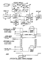
- Figure 1 is a block diagram of one type of decoder module, as installed in a CATV converter,
- Figure 2 is a wave form diagram of the decoder module of Figure 1 showing the relationship between suppressed horizontal sync, the sync gate, restored horizontal sync, and horizontal timing signals,
- Figure 3 is a program flow chart for the decoder module of Figure 1,
- Figure 4 is a block diagram of a decoder module arranged to decode another type of suppressed sync encoded video signal,
- Figure 5 is a waveform diagram of the VBI timing signal for the decoder module of Figure 4, and
- Figure 6 is a program flow chart of the decoder module of Figure 4.
- A great many of the currently used television encoding techniques suppress synchronizing pulses in order to render a TV picture unintelligible to an ordinary television set. Of the options currently in use, there is suppression of sync pulses during an entire video field and suppression of the sync pulses during picture video only, with both horizontal and vertical sync remaining at normal levels during the vertical blanking interval (VBI). Sync may be suppressed in a number of different ways. There may be a shift in the level of the sync pulses and this is done primarily when the video signal is at baseband frequency. Sync may also be suppressed by attenuation of the sync pulses at RF or at baseband and there may be a variation in the attenuation applied to the sync pulses on a field by field basis, and this variation may be random or may be related to some portion of the video signal. A suppressed horizontal sync pulse is shown in Figure 2. There is a leading guard band (before the H-sync pulse) and a trailing guard band (after the color burst), each of which is about 2 microseconds wide. The guard bands allow for a timing variation of the sync restoration gate generated in a decoder, which starts during the leading guard band and ends during the trailing guard band. The horizontal sync pulse and both guard bands normally occur during the overscan period on a TV screen and thus are invisible to the viewer.
- Under present cable television practice, once a particular cable system has committed to a particular type of video signal encoding, all decoders must be of the same type or must be the product of a single manufacturer. This unreasonably limits a particular cable company in its purchase of new decoders.
- The present invention provides a universal decoder in that the decoder module has multiple programs so that it may be used to decode several different types of sync suppressed video encoding. The decoder module may be used in connection with various types of cable television converters to the end that a cable system operator no longer will be required to buy decoders from a particular source, but rather can buy converters containing universal decoder modules from different sources. A cable system may also change over to a new encoding system gradually by installing new decoders that contain a universal decoder module that is compatible with the old encoding system.
- The present invention will be described in connection with a cable television converter that incorporates the type of encoding system shown in U.S. Patent 4,336,553 which is essentially the same type of encoding system as shown in U.S. Patents 4,340,906 and 4,353,088. It should be understood that the universal decoder module of the present invention can be used with any number of different cable television converters and/or decoders and in no sense should be limited to use with the specific encoding system disclosed in the '553 patent.
- In Figure 1, a
cable input 10 provides incoming video at RF to atuner 12. The output fromtuner 12, the video at a suitable intermediate frequency, is connected to anIF amplifier 14 which in turn is connected to a video demodulator 16 which provides the video signal at baseband or video frequency. The output from video demodulator 16 is connected through a resistor 18 to adecode module 20 which provides one of the inputs to avideo processor 22. - A sync separator 24 and a peak reading AGC circuit 26 receive inputs of baseband video, with the sync separator being effective to provide the horizontal sync timing signal (HEX) on line 27 and the vertical sync timing signal (VEX) on line 28. The HEX and VEX signals are provided to
video processor 22 and todecoder module 20. The output from the peak reading AGC circuit is connected toIF amplifier 14 which provides the gain for the amplifier to maintain the video signal in the converter/decoder at desired voltage levels. With the exception ofdecoder module 20, the remaining circuits are used in the commercial implementation of the encoding system of the '553 patent. - The video signal which is supplied to
tuner 10 has suppressed horizontal sync. In this particular embodiment of the invention the level of the sync has been suppressed only during the horizontal sync interval of the picture portion of the video. There is no suppression of horizontal or vertical sync during the VBI. Thedecode module 20 is effective to restore the level of the horizontal sync pulses which had been suppressed at the encoder and the video signal with restored horizontal sync during the picture video is the input tovideo processor 22. The HEX and VEX signals from the sync separator are used in the video processor and the fully restored video signal is then remodulated inmodulator 30 to a locally unused channel, forexample channel 3, as is conventional in cable television systems. -
Decoder module 20 includes a microprocessor 32 which may, for example, be an Intel 8051 type. Microprocessor 32 includes a CPU, program memory, data memory, I/O ports and other peripheral circuits such as a timer, all contained in one or more integrated circuit(s). Microprocessor 32 has HEX andVEX inputs video input 38. The microprocessor has an output online 40 which controls video signal inversion as will be described later. Microprocessor 32 also has an output online 42 to a transistor 44 which functions throughresistor 46 and resistor 18 as a pulldown circuit to restore the level of horizontal sync in accordance with instructions from the microprocessor. - Figure 2 shows the relationship between the waveform of suppressed horizontal sync, the sync gate, restored horizontal sync and HEX. Figure 3 is a flow chart for the program in the microprocessor which functions to control the outputs as described.
- In Figure 2, the normal IRE levels for a horizontal sync pulse and the color burst are indicated in that portion of the diagram designated "restored horizontal sync." The suppressed horizontal sync shows that the level of the sync pulse between the leading and trailing guard bands has been suppressed 70 IRE from a normal sync level of -40 IRE to a suppressed sync level of +30 IRE. The color burst has been similarly level changed. As mentioned above, the leading and trailing guard bands are each about 2 microseconds wide. Microprocessor 32 has an instruction cycle time of one microsecond and its clock signal is asynchronous to the incoming sync pulses of the video signal. The horizontal sync gate, generated by microprocessor 32, will thus have a timing variation (jitter) of one microsecond relative to the horizontal sync pulse. The horizontal sync gate, which is shown to have a one microsecond jitter, is shown between the suppressed horizontal sync waveform and the restored horizontal sync waveform, with the sync gate starting during the leading guard band and ending during the trailing guard band. The sync gate is used to control the restoration of horizontal sync to a normal IRE level. The HEX waveform in Figure 2 is triggered by and approximately coincident with the start of the horizontal sync pulse.
- The Figure 3 flow chart describes the program followed by microprocessor 32 in restoring the IRE levels of suppressed horizontal sync in a video baseband encoding or scrambling system in which the horizontal and vertical sync pulses in the VBI have not been suppressed. The
first step 48 in the program is a search for the VEX signal, and once there is a VEX input to the microprocessor, the next step, as represented at 50, is to determine the first HEX after VEX. A yes output fromstep 50 initiates step 52 which is to seek the last HEX in a particular vertical blanking interval. When there is an affirmative answer to the test ofstep 52, after a short delay represented bystep 54, the horizontal sync gate will begin, as represented bystep 56. As shown in Figure 2, the sync gate begins during the leading guard band and continues until its termination in the trailing guard band. The one microsecond jitter from the microprocesser clock, which occurs at the beginning and end of the sync gate and is shown in the restored sync, has no effect on the restored sync. After the sync gate has been turned on, as represented bystep 56, there is a short delay represented bystep 58, with the next step indicated at 60 representing a test as to whether or not the HEX signal is on. If the HEX signal is on, after a short delay indicated by step 62, the sync gate will be turned off, as represented bystep 64. If the HEX is not on at step 60, there is a short delay, +1 microsecond, represented bystep 66, after which the sync gate is turned off. - The difference between the delays, as represented by
steps 62 and 66, is the result of the one microsecond instruction cycle of the microprocessor and the fact that the spacing between horizontal sync pulses is approximately 63.5 microseconds. The microprocessor must switch between sync gate spacings of 63 and 64 microseconds. The HEX pulse is triggered by the restored horizontal sync and the microprocessor tests for a presence of HEX shortly after the start of the sync gate. If HEX is present at this time, a 63 microsecond spacing is selected. If HEX is not yet present, the spacing is 64 microseconds. - When the sync gate is turned off, as represented by
step 64, the next step is to determine if that is the end of the picture video, as represented bystep 68. If it is not the end of picture video, the program recycles to step 54, to provide horizontal sync gates to raise succeeding horizontal sync pulses in the picture video up to their proper IRE levels. If it is the end of the picture video, the program is recycled back to the beginning where the microprocessor will again search for VEX in the next VBI. - The decode module of Figure 1, having a microprocessor programmed in accordance with the flow chart of Figure 3 provides a horizontal sync gate to restore horizontal sync from the suppressed horizontal sync waveform of Figure 2 to the restored horizontal sync waveform of Figure 2. This particular example uses coding in the form of a 70 IRE level change for the horizontal sync pulses in the picture video, with the horizontal and vertical sync pulses in the VBI being unsuppressed. The decode module, as so programmed, can function to control decoding of any video signal which has been so encoded.
- Many video encoding systems also use video signal polarity inversion as a form of encoding. The decode module of Figure 1 has microprocessor 32 programmed so as to accomodate such polarity inversion. Only the active or picture video between horizontal sync pulses is inverted. The encoding system disclosed in the above-mentioned '553 patent has a video inversion circuit, as video polarity inversion is a normal part of the encoding disclosed in that patent. A video inversion sig-nal is developed by the microprocessor and provided on
line 40 to the video processor and used to control the inversion of the video signal. - When a field is to be inverted, a section of a line during the preceding VBI is elevated to 100 IRE. The line section normally has a zero IRE level. The inversion flag of 100 IRE in the VBI is detected by the microprocessor at the video input and an inversion gate is developed by the microprocessor and provided to the
video processor 22 in the period between horizontal sync gates. - The video inversion decoding portion of
decoder module 20 has been shown in connection with a particular type of sync suppression encoding. It should be understood that video signal polarity inversion may be used with any form of sync suppression encoding. - Figures 4, 5 and 6 relate to the use of the microprocessor based decoder module to decode a signal where each horizontal sync pulse is suppressed during picture video and the entire VBI (including horizontal and vertical sync) is also suppressed. Suppression is accomplished by an RF gated attenuator in the encoder. In order to decode such a video encoded signal, it is necessary to provide a timing signal and the timing signal will be placed in the VBI. Normally, such systems are decoded through the use of a timing signal carried as audio carrier amplitude modulation. However, the same decoding functions can be performed by the use of a timing signal in the VBI. In a mixed decoder system (with universal decoders added) both timing signals are carried simultaneously; the audio carrier signal for pre-existing decoders and the VBI signal for the universal decoders.
- As shown in Figure 5, the timing signal, which will be read by a positive peak reader in the decode module, begins with a solid 100 IRE signal in
line 10 which functions to charge the capacitor in the peak reader. Line 11 shows a known timing signal, again having a maximum level of 100 IRE.Line 12 is the complement of line 11. This particular combination of signal levels is extremely unlikely to occur on successive lines of active video and thus there is no likelihood of a false timing signal being utilized by the microprocessor. The VBI timing signal as shown in Figure 5 will have a data rate which is sufficiently slow so as to be read directly by the microprocessor in the decoder module. The head end video processor, which would add the VBI timing signal, may interface with the encoder to determine when the scrambling parameters, such as sync suppression depth, are being changed dynamically, and such changes can be inserted as data on another VBI horizontal line and passed to the decoder in real time. - Since an RF gated sync encoder attenuates the sync pulses, as opposed to level shifting as disclosed in the Figure 1-3 embodiment, the sync pull down circuit, illustrated in Figure 1, will not correctly restore horizontal sync and the color burst. An RF gated attenuator at the converter IF will properly restore the sync pulses.
- As shown in Figure 4, a tuner 80 has a cable input at 82. A
gated attenuator 84 is connected to the IF output of tuner 80, with the output from the attenuator being connected to anIF amplifier 86.Video demodulator 88, the microprocessor-baseddecode module 90, video processor 92,remodulator 94,peak reading AGC 96 and thesync separator circuit 98 are all comparable to the similarly designated circuits in Figure 1. The principal difference is that the sync gate frommicroprocesser 90, rather than causing a level change in the suppressed horizontal sync pulses, will increase the amplitude of the horizontal sync pulses and the entire VBI, as described in connection with the flow chart program of Figure 6. - In Figure 6, the
initial step 100 is the reset of the field counter, which controls the next step indicated at 102, which is a search for the VBI timing data illustrated in Figure 5. When the timing data is found, the sync gate input togated attenuator 84 will increase the gain during the VBI interval, as indicated bystep 104. The gain will remain at an increased level, to raise the amplitude of the horizontal and vertical sync pulses within the VBI, untilstep 106 which has a yes output at the end of the VBI. The VBI gate timing from thetiming data step 102 until the end ofstep 106 is determined by an internal timer in the microprocessor. The gain is then decreased, as indicated bystep 108, which provides the start of step 110, which times out at for the end of the field. At the end of the field, the gain is again increased, as indicated by step 112. The gain will remain at an increased level during the time that the microprocessor is searching for the VBI timing data, as indicated in step 114. This search will continue until either the VBI timing data is found or until the VBI search time-out period is reached, as indicated by step 116. If the VBI search times out, the gain will be lowered, as indicated atstep 118, and the entire cycle, beginning at the reset of the field counter, will be initiated. If the VBI timing data is found within the allocated search period, the number of fields counted is checked in step 120. If the VBI gain has been gated up for less than 20 consecutive fields, the field counter is incremented instep 122 and the cycle is repeated for another field. If the field counter count is 20, in step 120, the acquisition routine is exited. - The result of the program illustrated in Figure 6 is to settle the AGC control to provide proper IF gain and video signal level. The flow chart of Figure 6 describes what may be termed the acquisition portion of decoding. Once the VBI timing data has been successfully acquired by the microprocessor, the microprocessor enters the decode mode. This mode follows the program of Figure 3, except that the VBI timing signal is used instead of VEX and the gated attenuator is used to increase the signal level for the entire vertical blanking interval. By raising the gain of the entire vertical blanking interval, there is horizontal sync in that interval for use by the decoder to develop horizontal sync gates for the attenuated horizontal sync pulses of each horizontal line in the picture video. Thus, the program for decoding in the microprocessor for an attenuated sync pulse encoding system will function the same as the program for decoding in the sync level shifting encoding system, as shown in Figures 1-3, in that the restored horizontal and vertical sync in the VBI provides the timing for the horizontal sync gate which in turn increases the gain of the gated attenuator during the period of horizontal sync.
- The present invention provides a universal decoder module which has a microprocessor with multiple programs for use in decoding different types of encoded video signals. When it has been determined which type of encoding is used on a particular cable television system, and depending on whether the system has addressable converters, the selection of the particular program needed to decode the encoded video either can be communicated to a subscriber through the address format of the cable system, or if the individual subscribers are not individually addressable, then each decoder module may be mechanically configured to accept a particular type of encoding. Such a mechanical configuration could be by a hard wire, switch or otherwise.
- The invention provides a means whereby a particular cable system is not forever married to the converter/decoders of a particular manufacturer. The universal decoder is able, through one of its several programs, to decode many varieties of suppressed sync encoded video, whether or not video inversion is included in such. This has the advantage that the cable system operator may use different manufacturers' hardware and the decoder module may be used as an add-on to provide decoding for an otherwise non-decoding converter. However, some converters or decoders may not contain some of the circuitry which exists in the embodiment described above (such as the video inverter or sync separator) and this circuitry would have to be added.
- Whereas the preferred form of the invention has been shown and described herein, it should be realized that there may be many modifications, substitutions and alterations thereto.
Claims (17)
said decoder including a microprocessor programmed to first determine horizontal sync timing from timing signals in the VBI and second to provide a horizontal sync gate signal based on horizontal sync timing, which horizontal sync gate signal is effective to restore the suppressed horizontal sync pulses to an unsuppressed format.
using a microprocessor programmed to determine horizontal sync pulse timing from timing signals in the VBI and to provide a horizontal sync gate signal from said timing signal, which horizontal sync gate signal is used to restore suppressed horizontal sync pulses.
Applications Claiming Priority (2)
| Application Number | Priority Date | Filing Date | Title |
|---|---|---|---|
| US382899 | 1982-05-28 | ||
| US38289989A | 1989-07-21 | 1989-07-21 |
Publications (3)
| Publication Number | Publication Date |
|---|---|
| EP0409211A2 true EP0409211A2 (en) | 1991-01-23 |
| EP0409211A3 EP0409211A3 (en) | 1992-06-03 |
| EP0409211B1 EP0409211B1 (en) | 1995-07-05 |
Family
ID=23510887
Family Applications (1)
| Application Number | Title | Priority Date | Filing Date |
|---|---|---|---|
| EP90113788A Expired - Lifetime EP0409211B1 (en) | 1989-07-21 | 1990-07-18 | Universal decoder |
Country Status (14)
| Country | Link |
|---|---|
| EP (1) | EP0409211B1 (en) |
| JP (1) | JP2635202B2 (en) |
| AR (1) | AR244481A1 (en) |
| AT (1) | ATE124833T1 (en) |
| AU (1) | AU621762B2 (en) |
| BR (1) | BR9003532A (en) |
| CA (1) | CA2020313C (en) |
| DE (1) | DE69020654T2 (en) |
| DK (1) | DK0409211T3 (en) |
| ES (1) | ES2077612T3 (en) |
| GR (1) | GR3017056T3 (en) |
| IL (1) | IL94988A0 (en) |
| NO (1) | NO179060C (en) |
| PL (1) | PL163971B1 (en) |
Citations (4)
| Publication number | Priority date | Publication date | Assignee | Title |
|---|---|---|---|---|
| US4222068A (en) * | 1978-11-02 | 1980-09-09 | American Television And Communications Corporation | Subscription television apparatus and methods |
| US4336553A (en) * | 1980-05-14 | 1982-06-22 | Oak Industries | Method of coding audio and video signals |
| US4338628A (en) * | 1979-12-19 | 1982-07-06 | Dynacom International, Inc. | Scrambled video communication system |
| EP0187483A2 (en) * | 1985-01-02 | 1986-07-16 | General Instrument Corporation | Improved video encryption system |
Family Cites Families (6)
| Publication number | Priority date | Publication date | Assignee | Title |
|---|---|---|---|---|
| US4965825A (en) * | 1981-11-03 | 1990-10-23 | The Personalized Mass Media Corporation | Signal processing apparatus and methods |
| JPS60103789A (en) * | 1983-11-10 | 1985-06-08 | Sanyo Electric Co Ltd | Scramble system of television signal |
| US4571615A (en) * | 1983-06-10 | 1986-02-18 | General Instrument Corporation | Timing generator for sync suppressed television signals |
| JPS6260383A (en) * | 1985-09-10 | 1987-03-17 | Matsushita Electric Ind Co Ltd | Video signal processor |
| JPS63122388A (en) * | 1986-11-12 | 1988-05-26 | Hitachi Ltd | Synchronizing reproducing circuit |
| US4928309A (en) * | 1989-03-31 | 1990-05-22 | General Instrument Corporation | Method and apparatus for descrambling a television signal |
-
1990
- 1990-07-03 CA CA002020313A patent/CA2020313C/en not_active Expired - Fee Related
- 1990-07-05 IL IL94988A patent/IL94988A0/en not_active IP Right Cessation
- 1990-07-11 AU AU58903/90A patent/AU621762B2/en not_active Ceased
- 1990-07-18 DE DE69020654T patent/DE69020654T2/en not_active Expired - Fee Related
- 1990-07-18 AT AT90113788T patent/ATE124833T1/en not_active IP Right Cessation
- 1990-07-18 DK DK90113788.5T patent/DK0409211T3/en active
- 1990-07-18 EP EP90113788A patent/EP0409211B1/en not_active Expired - Lifetime
- 1990-07-18 ES ES90113788T patent/ES2077612T3/en not_active Expired - Lifetime
- 1990-07-20 BR BR909003532A patent/BR9003532A/en not_active IP Right Cessation
- 1990-07-20 NO NO903252A patent/NO179060C/en not_active IP Right Cessation
- 1990-07-20 AR AR90317430A patent/AR244481A1/en active
- 1990-07-20 PL PL90286151A patent/PL163971B1/en unknown
- 1990-07-21 JP JP2193785A patent/JP2635202B2/en not_active Expired - Fee Related
-
1995
- 1995-08-09 GR GR950402180T patent/GR3017056T3/en unknown
Patent Citations (4)
| Publication number | Priority date | Publication date | Assignee | Title |
|---|---|---|---|---|
| US4222068A (en) * | 1978-11-02 | 1980-09-09 | American Television And Communications Corporation | Subscription television apparatus and methods |
| US4338628A (en) * | 1979-12-19 | 1982-07-06 | Dynacom International, Inc. | Scrambled video communication system |
| US4336553A (en) * | 1980-05-14 | 1982-06-22 | Oak Industries | Method of coding audio and video signals |
| EP0187483A2 (en) * | 1985-01-02 | 1986-07-16 | General Instrument Corporation | Improved video encryption system |
Also Published As
| Publication number | Publication date |
|---|---|
| NO903252D0 (en) | 1990-07-20 |
| DK0409211T3 (en) | 1995-11-20 |
| JPH03101577A (en) | 1991-04-26 |
| IL94988A0 (en) | 1991-06-10 |
| ATE124833T1 (en) | 1995-07-15 |
| GR3017056T3 (en) | 1995-11-30 |
| NO179060B (en) | 1996-04-15 |
| JP2635202B2 (en) | 1997-07-30 |
| CA2020313A1 (en) | 1991-01-22 |
| AU5890390A (en) | 1991-01-24 |
| NO179060C (en) | 1996-08-28 |
| CA2020313C (en) | 1996-06-11 |
| DE69020654D1 (en) | 1995-08-10 |
| AU621762B2 (en) | 1992-03-19 |
| PL163971B1 (en) | 1994-06-30 |
| BR9003532A (en) | 1991-08-27 |
| NO903252L (en) | 1991-01-22 |
| AR244481A1 (en) | 1993-10-29 |
| EP0409211B1 (en) | 1995-07-05 |
| ES2077612T3 (en) | 1995-12-01 |
| DE69020654T2 (en) | 1995-11-30 |
| PL286151A1 (en) | 1992-01-27 |
| EP0409211A3 (en) | 1992-06-03 |
Similar Documents
| Publication | Publication Date | Title |
|---|---|---|
| US5113440A (en) | Universal decoder | |
| US4336553A (en) | Method of coding audio and video signals | |
| US4424532A (en) | Coding and decoding system for video and audio signals | |
| US4353088A (en) | Coding and decoding system for video and audio signals | |
| US4471380A (en) | Scrambling and descrambling of television signals for subscription TV | |
| US4340906A (en) | Video signal coding by video signal polarity reversal on the basis of brightness level comparison | |
| US4466017A (en) | Sync suppression scrambling of television signals for subscription TV | |
| CA1218143A (en) | Timing generator for sync suppressed television signals | |
| US4231063A (en) | Frame synchronizer having a write-inhibit circuit | |
| US3460161A (en) | Secrecy television apparatus with scrambled synchronizing signals | |
| US4511919A (en) | Method and apparatus for scrambling and descrambling video signals in a multichannel system | |
| US4145717A (en) | Subscription TV audio carrier recovery system | |
| EP0078976A2 (en) | Dynamic video scrambling | |
| US4590519A (en) | Television signal scrambling/descrambling system | |
| US4673975A (en) | Television signal scrambling apparatus | |
| GB2038137A (en) | Coding and decoding of TV signals | |
| US4636852A (en) | Scrambling and descrambling of television signals for subscription TV | |
| EP0409211B1 (en) | Universal decoder | |
| US4463376A (en) | Television signal processing system for a wireless pay system | |
| US5861925A (en) | Multiplexed text data sampling circuit | |
| KR0152079B1 (en) | Automatic frequency control method and receiving apparatus using thereof | |
| US4802214A (en) | Method and apparatus for identifying and rendering operative particular descramblers in a television signal scrambling system | |
| JPS58157281A (en) | Phase alternation type dynamic scramble | |
| US4613900A (en) | Digital code reading apparatus and method | |
| US3466385A (en) | Correlation testing arrangement for a subscription television receiver |
Legal Events
| Date | Code | Title | Description |
|---|---|---|---|
| PUAI | Public reference made under article 153(3) epc to a published international application that has entered the european phase |
Free format text: ORIGINAL CODE: 0009012 |
|
| AK | Designated contracting states |
Kind code of ref document: A2 Designated state(s): AT BE CH DE DK ES FR GB GR IT LI LU NL SE |
|
| PUAL | Search report despatched |
Free format text: ORIGINAL CODE: 0009013 |
|
| AK | Designated contracting states |
Kind code of ref document: A3 Designated state(s): AT BE CH DE DK ES FR GB GR IT LI LU NL SE |
|
| 17P | Request for examination filed |
Effective date: 19920630 |
|
| 17Q | First examination report despatched |
Effective date: 19940414 |
|
| RAP1 | Party data changed (applicant data changed or rights of an application transferred) |
Owner name: TV/COM TECHNOLOGIES, INC. |
|
| GRAA | (expected) grant |
Free format text: ORIGINAL CODE: 0009210 |
|
| AK | Designated contracting states |
Kind code of ref document: B1 Designated state(s): AT BE CH DE DK ES FR GB GR IT LI LU NL SE |
|
| REF | Corresponds to: |
Ref document number: 124833 Country of ref document: AT Date of ref document: 19950715 Kind code of ref document: T |
|
| REF | Corresponds to: |
Ref document number: 69020654 Country of ref document: DE Date of ref document: 19950810 |
|
| ITF | It: translation for a ep patent filed |
Owner name: JACOBACCI & PERANI S.P.A. |
|
| ET | Fr: translation filed | ||
| REG | Reference to a national code |
Ref country code: GR Ref legal event code: FG4A Free format text: 3017056 |
|
| REG | Reference to a national code |
Ref country code: DK Ref legal event code: T3 |
|
| REG | Reference to a national code |
Ref country code: ES Ref legal event code: FG2A Ref document number: 2077612 Country of ref document: ES Kind code of ref document: T3 |
|
| PLBE | No opposition filed within time limit |
Free format text: ORIGINAL CODE: 0009261 |
|
| STAA | Information on the status of an ep patent application or granted ep patent |
Free format text: STATUS: NO OPPOSITION FILED WITHIN TIME LIMIT |
|
| 26N | No opposition filed | ||
| PGFP | Annual fee paid to national office [announced via postgrant information from national office to epo] |
Ref country code: SE Payment date: 20010727 Year of fee payment: 12 Ref country code: DK Payment date: 20010727 Year of fee payment: 12 Ref country code: AT Payment date: 20010727 Year of fee payment: 12 |
|
| PGFP | Annual fee paid to national office [announced via postgrant information from national office to epo] |
Ref country code: LU Payment date: 20010730 Year of fee payment: 12 |
|
| PGFP | Annual fee paid to national office [announced via postgrant information from national office to epo] |
Ref country code: GR Payment date: 20010731 Year of fee payment: 12 |
|
| PGFP | Annual fee paid to national office [announced via postgrant information from national office to epo] |
Ref country code: BE Payment date: 20010801 Year of fee payment: 12 |
|
| PGFP | Annual fee paid to national office [announced via postgrant information from national office to epo] |
Ref country code: CH Payment date: 20010807 Year of fee payment: 12 |
|
| REG | Reference to a national code |
Ref country code: GB Ref legal event code: IF02 |
|
| PG25 | Lapsed in a contracting state [announced via postgrant information from national office to epo] |
Ref country code: LU Free format text: LAPSE BECAUSE OF NON-PAYMENT OF DUE FEES Effective date: 20020718 Ref country code: AT Free format text: LAPSE BECAUSE OF NON-PAYMENT OF DUE FEES Effective date: 20020718 |
|
| PG25 | Lapsed in a contracting state [announced via postgrant information from national office to epo] |
Ref country code: SE Free format text: LAPSE BECAUSE OF NON-PAYMENT OF DUE FEES Effective date: 20020719 |
|
| PG25 | Lapsed in a contracting state [announced via postgrant information from national office to epo] |
Ref country code: LI Free format text: LAPSE BECAUSE OF NON-PAYMENT OF DUE FEES Effective date: 20020731 Ref country code: DK Free format text: LAPSE BECAUSE OF NON-PAYMENT OF DUE FEES Effective date: 20020731 Ref country code: CH Free format text: LAPSE BECAUSE OF NON-PAYMENT OF DUE FEES Effective date: 20020731 Ref country code: BE Free format text: LAPSE BECAUSE OF NON-PAYMENT OF DUE FEES Effective date: 20020731 |
|
| BERE | Be: lapsed |
Owner name: *TV/COM TECHNOLOGIES INC. Effective date: 20020731 |
|
| PG25 | Lapsed in a contracting state [announced via postgrant information from national office to epo] |
Ref country code: GR Free format text: LAPSE BECAUSE OF NON-PAYMENT OF DUE FEES Effective date: 20030206 |
|
| REG | Reference to a national code |
Ref country code: DK Ref legal event code: EBP |
|
| EUG | Se: european patent has lapsed | ||
| REG | Reference to a national code |
Ref country code: CH Ref legal event code: PL |
|
| PGFP | Annual fee paid to national office [announced via postgrant information from national office to epo] |
Ref country code: NL Payment date: 20030731 Year of fee payment: 14 |
|
| PGFP | Annual fee paid to national office [announced via postgrant information from national office to epo] |
Ref country code: FR Payment date: 20040630 Year of fee payment: 15 |
|
| PGFP | Annual fee paid to national office [announced via postgrant information from national office to epo] |
Ref country code: GB Payment date: 20040702 Year of fee payment: 15 |
|
| PGFP | Annual fee paid to national office [announced via postgrant information from national office to epo] |
Ref country code: ES Payment date: 20040719 Year of fee payment: 15 |
|
| PGFP | Annual fee paid to national office [announced via postgrant information from national office to epo] |
Ref country code: DE Payment date: 20040729 Year of fee payment: 15 |
|
| PG25 | Lapsed in a contracting state [announced via postgrant information from national office to epo] |
Ref country code: NL Free format text: LAPSE BECAUSE OF NON-PAYMENT OF DUE FEES Effective date: 20050201 |
|
| NLV4 | Nl: lapsed or anulled due to non-payment of the annual fee |
Effective date: 20050201 |
|
| PG25 | Lapsed in a contracting state [announced via postgrant information from national office to epo] |
Ref country code: IT Free format text: LAPSE BECAUSE OF NON-PAYMENT OF DUE FEES;WARNING: LAPSES OF ITALIAN PATENTS WITH EFFECTIVE DATE BEFORE 2007 MAY HAVE OCCURRED AT ANY TIME BEFORE 2007. THE CORRECT EFFECTIVE DATE MAY BE DIFFERENT FROM THE ONE RECORDED. Effective date: 20050718 Ref country code: GB Free format text: LAPSE BECAUSE OF NON-PAYMENT OF DUE FEES Effective date: 20050718 |
|
| PG25 | Lapsed in a contracting state [announced via postgrant information from national office to epo] |
Ref country code: ES Free format text: LAPSE BECAUSE OF NON-PAYMENT OF DUE FEES Effective date: 20050719 |
|
| PG25 | Lapsed in a contracting state [announced via postgrant information from national office to epo] |
Ref country code: DE Free format text: LAPSE BECAUSE OF NON-PAYMENT OF DUE FEES Effective date: 20060201 |
|
| GBPC | Gb: european patent ceased through non-payment of renewal fee |
Effective date: 20050718 |
|
| PG25 | Lapsed in a contracting state [announced via postgrant information from national office to epo] |
Ref country code: FR Free format text: LAPSE BECAUSE OF NON-PAYMENT OF DUE FEES Effective date: 20060331 |
|
| REG | Reference to a national code |
Ref country code: FR Ref legal event code: ST Effective date: 20060331 |
|
| REG | Reference to a national code |
Ref country code: ES Ref legal event code: FD2A Effective date: 20050719 |