EP0406469B1 - Digital control circuit for tuning systems - Google Patents
Digital control circuit for tuning systems Download PDFInfo
- Publication number
- EP0406469B1 EP0406469B1 EP89112332A EP89112332A EP0406469B1 EP 0406469 B1 EP0406469 B1 EP 0406469B1 EP 89112332 A EP89112332 A EP 89112332A EP 89112332 A EP89112332 A EP 89112332A EP 0406469 B1 EP0406469 B1 EP 0406469B1
- Authority
- EP
- European Patent Office
- Prior art keywords
- digital
- data
- control circuit
- bit
- output
- Prior art date
- Legal status (The legal status is an assumption and is not a legal conclusion. Google has not performed a legal analysis and makes no representation as to the accuracy of the status listed.)
- Expired - Lifetime
Links
- 230000010354 integration Effects 0.000 claims description 24
- 238000009499 grossing Methods 0.000 claims description 18
- 230000003068 static effect Effects 0.000 claims description 9
- 230000008859 change Effects 0.000 claims description 6
- 230000015572 biosynthetic process Effects 0.000 claims description 5
- 238000003786 synthesis reaction Methods 0.000 claims description 5
- 125000004122 cyclic group Chemical group 0.000 claims description 2
- 238000010586 diagram Methods 0.000 description 11
- 230000006870 function Effects 0.000 description 8
- 230000009977 dual effect Effects 0.000 description 7
- 230000008901 benefit Effects 0.000 description 5
- 230000007774 longterm Effects 0.000 description 4
- 238000001308 synthesis method Methods 0.000 description 3
- 230000010355 oscillation Effects 0.000 description 2
- 230000006399 behavior Effects 0.000 description 1
- 230000002457 bidirectional effect Effects 0.000 description 1
- 238000006243 chemical reaction Methods 0.000 description 1
- 238000013479 data entry Methods 0.000 description 1
- 230000001419 dependent effect Effects 0.000 description 1
- 230000004069 differentiation Effects 0.000 description 1
- 238000000034 method Methods 0.000 description 1
- 238000001208 nuclear magnetic resonance pulse sequence Methods 0.000 description 1
- 230000008569 process Effects 0.000 description 1
- 239000004065 semiconductor Substances 0.000 description 1
Images

Classifications
-
- H—ELECTRICITY
- H03—ELECTRONIC CIRCUITRY
- H03J—TUNING RESONANT CIRCUITS; SELECTING RESONANT CIRCUITS
- H03J7/00—Automatic frequency control; Automatic scanning over a band of frequencies
-
- H—ELECTRICITY
- H03—ELECTRONIC CIRCUITRY
- H03L—AUTOMATIC CONTROL, STARTING, SYNCHRONISATION OR STABILISATION OF GENERATORS OF ELECTRONIC OSCILLATIONS OR PULSES
- H03L7/00—Automatic control of frequency or phase; Synchronisation
- H03L7/06—Automatic control of frequency or phase; Synchronisation using a reference signal applied to a frequency- or phase-locked loop
- H03L7/16—Indirect frequency synthesis, i.e. generating a desired one of a number of predetermined frequencies using a frequency- or phase-locked loop
- H03L7/18—Indirect frequency synthesis, i.e. generating a desired one of a number of predetermined frequencies using a frequency- or phase-locked loop using a frequency divider or counter in the loop
- H03L7/183—Indirect frequency synthesis, i.e. generating a desired one of a number of predetermined frequencies using a frequency- or phase-locked loop using a frequency divider or counter in the loop a time difference being used for locking the loop, the counter counting between fixed numbers or the frequency divider dividing by a fixed number
- H03L7/187—Indirect frequency synthesis, i.e. generating a desired one of a number of predetermined frequencies using a frequency- or phase-locked loop using a frequency divider or counter in the loop a time difference being used for locking the loop, the counter counting between fixed numbers or the frequency divider dividing by a fixed number using means for coarse tuning the voltage controlled oscillator of the loop
- H03L7/189—Indirect frequency synthesis, i.e. generating a desired one of a number of predetermined frequencies using a frequency- or phase-locked loop using a frequency divider or counter in the loop a time difference being used for locking the loop, the counter counting between fixed numbers or the frequency divider dividing by a fixed number using means for coarse tuning the voltage controlled oscillator of the loop comprising a D/A converter for generating a coarse tuning voltage
Definitions
- Devices for receiving high-frequency signals contain control devices with which a local oscillator required for frequency conversion is set to the correct oscillation frequency.
- the voltage-dependent capacitance of tuner diodes is generally used to vary the natural frequency of high-frequency oscillators in a wide range.
- tuner diodes are used at the same time, the control characteristics of which are paired in order to ensure capacity synchronization with different tuner tuning voltages.
- a monolithically integrated, digital control circuit for tuning systems of television receivers is described Device for generating a Has tuner tuning voltage according to the voltage synthesis process.
- PDM signal pulse density modulated pulse sequence
- This signal is smoothed by means of a multi-stage low-pass filter to give the tuner tuning voltage that is constant over time.
- This described device for generating the tuner tuning voltage is accordingly a dynamic digital-to-analog converter which forms the desired high-resolution analog signal from the stored data by means of a pulse density modulator.
- the control circuit described also contains four further dynamic digital-to-analog converters which generate low-resolution analog function setting voltages from stored data, e.g. for volume or brightness adjustment.
- the control circuit also has a timing and control device for the individual functional sequences. Via a data entry device, e.g. an externally accessible data bus, the data stored under various addresses in the digital storage unit can be read in, called up or changed.
- the respective TV channel number which is activated via a remote control circuit, serves as the address, for example.
- a disadvantage of such analog or digital PLL control loops in tuning systems is, however, that they require a low-pass filter with a very low cut-off frequency or an integrator that slows the change from one frequency to another in order to suppress oscillation and to smooth the tuner tuning voltage.
- This is a hindrance where a single tuner is to be switched quickly between several signal sources, for example in the case of multiple image reproduction in the television receiver or in the case of a frequency diversity reception device in the car radio. If the switchover takes too long, some of the information is lost.
- multi-tuner versions are usually forbidden in the entertainment area for cost reasons.
- WO-A 88/01113 describes a digital control circuit for tuning systems which enables a rapid change in the tuner tuning voltage by means of a data setting device and a PLL circuit, cf. the preambles of independent claims 1 and 9.
- WO-A-87/07794 describes a similar circuit for generating a tuner tuning voltage, in which the usual functional elements of the associated PLL circuit are described in detail.
- the accuracy of the tuning voltage depends on the accuracy of a static digital-to-analog converter, which is controlled with a digital word of the appropriate number of digits.
- the required high resolution requires correspondingly complex digital-to-analog converters with an accuracy of 12 to 14 bits. As is generally known, this accuracy is difficult to achieve in monolithic integration.
- This object is achieved according to the invention with the features specified in independent claim 1 or independent claim 9.
- the low-pass filter required according to the invention has only a small time constant, which enables the desired smoothing of the output signals with a short running-in time.
- Another advantage of the invention is that a digital control circuit for tuning systems is specified, in which as many functions as possible can be carried out via already existing functional devices. This is particularly important if the digital control circuit contains a programmable microprocessor that can take over these functions in the form of microprogram sequences.
- a digital control circuit 1 for high-frequency tuning systems is connected via a data input device 8 to an external data bus 8a which is, for example, externally fed by a remote control receiver 8b.
- the digital control circuit 1 is supplied with a wide variety of data via the data input device 8, which either serve to change the channel or change certain function setting voltages s1, s2, s3, such as volume, brightness, etc.
- the function setting voltages s1, s2, s3 are generated by first, relatively low-resolution digital-to-analog converters 3, 4, 5, of which three are shown in FIG. 1, for example.
- the data input of these digital-to-analog converters takes place via a Buffer 18 from the digital storage device 6.
- the central control function in the digital control circuit 1 is carried out by a timing and control device 7, which generates control commands st and a central control clock cl for all subcircuits.
- the digital control circuit 1 contains, as an essential functional part, a device 2 for generating a tuner tuning voltage vt.
- the tuner tuning voltage vt must have a very high resolution in the voltage range between 0.5 V and 33 V, for example 16 bits (in the dual number code ). This requires completely different digital-to-analog converters than when generating the function setting voltages. Such a high-resolution digital-to-analog converter can therefore hardly be realized as a static converter with a monotonous characteristic. For this reason, the principle of the dynamic converter shown in FIG.
- PDM signal pulse-density-modulated signal
- the frequency synthesis system shown in FIG. 1 contains a phase locked loop 13, which comprises a tuner 22 and the device 2 for generating the tuner tuning voltage vt.
- the tuner 22 is also supplied with the high-frequency antenna signal h.
- the oscillator signal fo is fed to the frequency divider input of a programmable frequency divider 15, the control input of which is fed with the division number tz from the digital memory device 6.
- the output of the programmable frequency divider 15 is connected to the signal input of a phase comparator 16, the reference input of which is fed with a reference signal for a fixed frequency.
- the reference signal fr can be derived, for example, from the system clock cl.
- the division number tz can also be a non-complete division number.
- phase comparator 16 the output of which generates an up or down signal
- a digital integrator 10 which corresponds to the respective Gives integration value i, for example a 16-digit data value in the dual number code
- second digital-to-analog converter 9 of high resolution
- the digital integrator 10 has an attachment device 10a, by means of which the digital integrator 10 can be set to an arbitrarily predeterminable value at any time. This takes place via a first data line 11, via which the default data value id is supplied to the digital integrator 10 from the digital storage device 6.
- the value that corresponds to the steady-state integration value i is advantageously selected as the default data value id when the phase-locked loop 13 is locked to the correct local frequency. Because of the non-linear characteristic of the tuner diodes, this integration value i must be determined in a separate measuring step. This is done, for example, when programming the desired channel for the first time.
- the steady-state integration value i is transmitted to the digital storage device 6 via the second data line 12 and is stored there together with the associated number of divisions tz at the address of this channel.
- this stored integration value i arrives as the preset data value id via the first data line 11 on the attachment device 10a of the digital integrator 10.
- phase locked loop 13 is thus close to the steady state and the frequency of the VCO 14 has been switched over almost without delay. At most, a slight correction over a few incrementing steps at the up / down increment input 10b is required.
- the final integration value i would only be set after a large number of increment or decrement steps.
- the run-in time would also depend on the step size of the tuner tuning voltage vt.
- the first and the second data line 11, 12 can be combined as a bidirectional data line.
- the presetting of the digital integrator 10 is not necessary for the relatively slow search run, because the integration value i is only changed via increment steps.
- the search is usually carried out when starting up for the first time, in which case the digital storage device 6 does not yet contain any default data values id.
- Such a digital-to-analog converter could directly drive the VCO 14 without an analog smoothing filter. The characteristic curve would not even have to be linear.
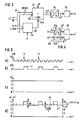
- a dynamic digital-to-analog converter is shown schematically as a block diagram in FIG. 2, namely a known pulse density modulator 20, which essentially consists of an accumulator 26, 27 and which has only an overflow output 26a as an output.
- the integration value i represents an m-digit data word in the dual number code that is fed to the first data input of an m-digit adder 26.
- the m-digit output of this adder 26 is connected to the input of an accumulator memory 27, the output of which is connected to the m-digit second input of the adder 26.
- the accumulator 26, 27 of the pulse density modulator 20 is clocked by the system clock cl.
- a smoothing low-pass filter 19 which consists of several RC elements connected in series, serves to smooth the PDM signal p1.
- the constant tuner tuning voltage vt can then be tapped at the output of the smoothing low pass 19.
- the time constant of the smoothing low pass 19 depends directly on the long-term period of the PDM signal p1. The higher the resolution of the dynamic digital-to-analog converter, the greater the number of digits m of the adder 26 and the greater the long-term or repetition period of the PDM signal p1 can become.
- FIG. 3 an embodiment of a dynamic digital-to-analog converter according to the invention from FIG. 1 is shown schematically as a block diagram which, despite the high resolution, only requires an analog smoothing filter 25 with a small time constant, which is also provided in an analog manner.
- the m-digit integration value i (in the dual number code) is split into two data parts, with n higher-order digits forming the higher-order data part ih and the other mn remaining digits forming the lower-order data part il.
- the n-digit data part ih is fed to the n digits of the first data input 21a of an (n + 1) digit adder 21, the n + 1 digits relating to the data volume of the output.
- the least significant digit of the most significant data part ih is connected to the LSB digit of the first data input 21a.
- the low-order data part il is fed with an (mn) -digit pulse density modulator 23, the output-side PDM signal p2 of which is fed to the second data input 21b, specifically the LSB point of the (n + 1) -digit adder 21. Since the sum of the higher-order data part ih and the PDM signal p2 can be a maximum of 2 n , but with n digits only the value 2 n -1 can be realized, the output signal of the adder must have 21 n + 1 digits in the binary number code.
- n + 1) digit digital-to-analog converter 24 The output signal of this converter 24 fluctuates by exactly one LSB in time with the PDM signal p2. This slight pulse disturbance can be easily leveled by means of a smoothing filter 25 with a small time constant, so that the unsmoothed tuner tuning voltage vt 'becomes a ripple-free signal.
- This measure according to the invention makes it possible to implement a high-resolution digital-to-analog converter which is static for the coarse adjustment range and for the Fine adjustment range advantageously combines the dynamic implementation principle.
- the small number of digits of the static digital-to-analog converter 24 and the small time constant sufficient for smoothing, which is realized by a simple smoothing filter 25, are particularly advantageous.
- the statically set rough adjustment range also acts as an analog setting for the smoothing filter.
- Such a digital-to-analog converter can advantageously be used in the digital control circuit 1 for tuning systems in which the quickly switchable tuner tuning voltage vt is formed by the device 2 according to the voltage synthesis method.
- the small time constant of the analog smoothing filter 25 then represents the only delay, as in frequency synthesis, which does not, however, interfere.
- FIG. 4 schematically shows a particularly advantageous development of the circuit arrangement according to FIG. 3.
- the (n + 1) -digit digital-analog converter 24 according to FIG. 3 can be replaced by an n-digit digital-analog converter 24a, which is only equipped with an additional, separate LSB stage 24c have to be.
- the n digits of the higher-order data part ih directly feed the input of the actual n-digit digital-to-analog converter 24b, while the PDM signal p2 is fed to the input of the separate LSB stage 24c.
- the output signal of the actual n-digit digital-to-analog converter 24b is a constant basic value ih ', which is fed to the first input of an analog adder 28.
- the output of the separate LSB stage 24c provides an amplitude-correct PDM signal p2 'which is fed to the second input of the analog adder 28.
- the amplitude-correct PDM signal p2 ' has an accurate LSB level value regardless of the level of the pulse density modulator 23.
- the output signal of the analog adder 28 corresponds exactly to the unsmoothed tuner tuning voltage vt 'of Fig.3.
- FIG. 5 the functioning of this circuit arrangement according to FIG. 3 or 4 is illustrated in FIG. 5 on the basis of some typical signal curves.
- the binary number 1101 with the decimal value 13 is assumed as the supplied integration value i.
- the higher order data part ih thus consists of the binary number 11 (decimal value 3) and the lower order data part il consists of the dual number 01 (decimal value 1).
- the timing diagram 5a shows the system clock cl, whose pulse-pause ratio is 1: 1.
- the time diagram 5b shows the PDM signal p2 of the (mn) digit pulse density modulator 23.
- the counter content of the pulse density modulator 23 is the dual number 01 (decimal value 1) accepted. This results in an overflow at the third clock pulse t3, which appears as a logic "1" in the PDM signal p2. This overflow appears after every four clock pulses. This corresponds to the ratio of the data value supplied, namely the decimal value 1, to the number of possible differentiation levels, namely four in the example shown.
- the constant basic value ih ' is shown with the decimal value 3.
- This constant basic value ih ' is not present as the actual signal in the circuit arrangement according to FIG. 3, but is readily obtained as an intermediate step from the higher-value data part ih or directly as a signal from FIG.
- the timing diagram 5d finally shows the unsmoothed tuner tuning signal vt 'from Fig.3 and Fig.4, which consists of the combination of the constant basic value ih' and the amplitude-correct PDM signal p2 '.
- the constant basic value ih 'and the amplitude-correct PDM signal p2' are only included as real signals in FIG.
- the unsmoothed tuner tuning voltage vt ' jumps from decimal value 3 by one LSB value to decimal value 4. The same thing is repeated every four clock pulses.
- the arithmetic mean is formed during smoothing, so that the tuner tuning voltage vt, which is drawn as a dash-dotted line, is (LSB) / 4 above the decimal value 3.
- a particularly advantageous development of the invention consists in that the digital control circuit 1 contains a large number of devices 2 for generating different tuner tuning voltages. This enables the use of unpaired tuner diodes by storing the different tuning data of these tuner diodes under a common address in the digital memory device 6. For each digital integrator 10 or digital low-pass filter, the respective default data value id must also be stored under the same address.
- the digital control circuit 1 in the timing and control device 7 with a programmable microprocessor 29, which controls the cyclic switching of the reception channels, for example when receiving multi-channel television signals.
- the required data such as the channel numbers, playback sequence, dwell time or cycle duration can then be entered as a program via the data input device.
- the use of a program enables a wide variety of applications to be covered with a single digital control circuit 1. This is a very economical solution, especially in the consumer sector.
- the circuitry can be kept small, even if a variety of tuner tuning voltages vt should be generated. Except for the output stages of the digital-to-analog converters 9, 24, 24a, the functional parts are then only actually present once, or are even implemented in software technology.
Landscapes
- Channel Selection Circuits, Automatic Tuning Circuits (AREA)
Description
Geräte zum Empfang hochfrequenter Signale enthalten Steuereinrichtungen, mit denen ein zur Frequenzumsetzung erforderlicher lokaler Oszillator auf die richtige Schwingungsfrequenz gesetzt wird. Hierzu wird in der Regel die spannungsabhängige Kapazität von Tunerdioden ausgenutzt, um die Eigenfrequenz von Hochfrequenz-Oszillatoren in weiten Bereichen zu variieren. Meist sind dabei gleichzeitig mehrere Tunerdioden im Einsatz, deren Steuerkennlinien gepaart sind, um einen Kapazitätsgleichlauf bei unterschiedlichen Tuner-Abstimmspannungen zu gewährleisten.Devices for receiving high-frequency signals contain control devices with which a local oscillator required for frequency conversion is set to the correct oscillation frequency. For this purpose, the voltage-dependent capacitance of tuner diodes is generally used to vary the natural frequency of high-frequency oscillators in a wide range. Usually, several tuner diodes are used at the same time, the control characteristics of which are paired in order to ensure capacity synchronization with different tuner tuning voltages.
Die manuelle Einstellung der Tuner-Abstimmspannung wird bei modernen Geräten vorteilhafterweise immer mehr durch digitale Steuerschaltungen ersetzt, wobei die Langzeitkonstanz und die Genauigkeit in der Einstellung und Reproduzierbarkeit erheblich gesteigert ist. Es wird dabei zwischen Spannungs- und Frequenzsyntheseverfahren unterschieden, wobei letztere eine Phasenregelschleife (= PLL) enthalten, welche die definierte Einstellung beliebiger lokaler Oszillatorfrequenzen erlaubt.The manual adjustment of the tuner tuning voltage is more and more advantageously being replaced by digital control circuits in modern devices, the long-term constancy and the accuracy in the setting and reproducibility being considerably increased. A distinction is made between voltage and frequency synthesis methods, the latter containing a phase locked loop (= PLL), which allows the defined setting of any local oscillator frequencies.
In der "ITT Semiconductors" Firmendruckschrift, "SAA 1290, Remote-Control and Tuning IC for TV Receivers", Ausgabe 1986, Juli, Bestellnummer 6251-222-5E ist beispielsweise eine monolithisch integrierte, digitale Steuerschaltung für Abstimmsysteme von Fernsehempfängern beschrieben, die eine Einrichtung zur Erzeugung einer Tuner-Abstimmspannung nach dem Spannungssyntheseverfahren aufweist. Als Ausgangssignal wird eine pulsdichtemodulierte Impulsfolge (= PDM-Signal) abgegeben, die über externe Schalteinrichtungen ein PDM-Signal mit einer Amplitude von 33 V erzeugt. Dieses Signal wird mittels eines mehrgliedrigen Tiefpasses geglättet, um die zeitlich konstante Tuner-Abstimmspannung zu ergeben. Es handelt sich hier bei dieser beschriebenen Einrichtung zur Erzeugung der Tuner-Abstimmspannung demnach um einen dynamischen Digital-Analogumsetzer, der aus den abgelegten Daten mittels eines Pulsdichtemodulators das gewünschte Analogsignal hoher Auflösung bildet.For example, in the "ITT Semiconductors" company publication, "SAA 1290, Remote Control and Tuning IC for TV Receivers", edition 1986, July, order number 6251-222-5E, a monolithically integrated, digital control circuit for tuning systems of television receivers is described Device for generating a Has tuner tuning voltage according to the voltage synthesis process. A pulse density modulated pulse sequence (= PDM signal) is emitted as the output signal, which generates a PDM signal with an amplitude of 33 V via external switching devices. This signal is smoothed by means of a multi-stage low-pass filter to give the tuner tuning voltage that is constant over time. This described device for generating the tuner tuning voltage is accordingly a dynamic digital-to-analog converter which forms the desired high-resolution analog signal from the stored data by means of a pulse density modulator.
Die beschriebene Steuerschaltung enthält ferner vier weitere dynamische Digital-Analogumsetzer, die aus gespeicherten Daten analoge Funktions-Einstellspannungen geringer Auflösung erzeugen, z.B. für die Lautstärke- oder Helligkeitseinstellung. Schließlich weist die Steuerschaltung auch eine Zeitablauf- und Steuereinrichtung für die einzelnen Funktionsabläufe auf. Über eine Dateneingabeeinrichtung, z.B. ein extern zugänglichen Datenbus, können die unter verschiedenen Adressen in der digitalen Speichereinheit abgespeicherten Daten eingelesen, abgerufen oder verändert werden. Als Adresse dient beispielsweise die jeweilige Fernseh-Kanalnummer, die über eine Fernbedienungsschaltung aktiviert wird.The control circuit described also contains four further dynamic digital-to-analog converters which generate low-resolution analog function setting voltages from stored data, e.g. for volume or brightness adjustment. Finally, the control circuit also has a timing and control device for the individual functional sequences. Via a data entry device, e.g. an externally accessible data bus, the data stored under various addresses in the digital storage unit can be read in, called up or changed. The respective TV channel number, which is activated via a remote control circuit, serves as the address, for example.
In der Offenlegungsschrift DE-A 34 27 852 (= US-A-4 544 911 und US-A-4 595 910) ist eine digitale Steuerschaltung für Abstimmsysteme in Fernsehempfängern beschrieben, die nach dem Frequenzsyntheseverfahren - also mit einer PLL-Regelschleife - arbeitet. Bei ihr wird die Tuner-Abstimmspannung ebenfalls mittels eines dynamischen Digital-Analogumsetzers erzeugt. Als Pulsdichtemodulator - in der Offenlegungsschrift Digital-Tastverhältnis-Steuerung genannt - wird ein akkumulierender Zähler verwendet, dessen Zähleingang mit einem aufzuaddierenden Datenwort gespeist ist und dessen Überlaufausgang das PDM-Signal liefert. Dabei tritt das Überlaufsignal in einem Betrachtungszeitraum im zeitlichen Mittel in demjenigen Verhältnis auf, das dem Zahlenverhältnis gleich ist, das aus dem Wert des zu addierenden Datenworts und der Anzahl der möglichen Zählerpositionen zu bilden ist.In the published patent application DE-A 34 27 852 (= US-A-4 544 911 and US-A-4 595 910) is a digital Control circuit for tuning systems in television receivers described, which works according to the frequency synthesis method - ie with a PLL control loop. With it, the tuner tuning voltage is also generated by means of a dynamic digital-to-analog converter. An accumulating counter is used as the pulse density modulator - called digital duty cycle control in the published patent application - the counter input of which is fed with a data word to be added and the overflow output of which supplies the PDM signal. The overflow signal occurs over a period of time on average in the ratio that is equal to the numerical ratio that is to be formed from the value of the data word to be added and the number of possible counter positions.
Ein Nachteil derartiger analoger oder digitaler PLL-Regelschleifen in Abstimmsystemen ist indessen, daß sie zur Schwingungsunterdrückung und zur Glättung der Tuner-Abstimmspannung einen Tiefpaß mit sehr niedriger Grenzfrequenz oder einen Integrator benötigen, der den Wechsel von einer Frequenz auf eine andere verlangsamt. Dies ist dort hinderlich, wo ein einziger Tuner rasch zwischen mehreren Signalquellen umgeschaltet werden soll, z.B. bei einer Mehrfachbildwiedergabe im Fernsehempfänger oder bei einer Frequenz-Diversity-Empfangseinrichtung im Autoradio. Dauert die Umschaltung zu lang, geht ein Teil der Information verloren. Andererseits verbieten sich Mehrtunerausführungen im Unterhaltungsbereich meist aus Kostengründen.A disadvantage of such analog or digital PLL control loops in tuning systems is, however, that they require a low-pass filter with a very low cut-off frequency or an integrator that slows the change from one frequency to another in order to suppress oscillation and to smooth the tuner tuning voltage. This is a hindrance where a single tuner is to be switched quickly between several signal sources, for example in the case of multiple image reproduction in the television receiver or in the case of a frequency diversity reception device in the car radio. If the switchover takes too long, some of the information is lost. On the other hand, multi-tuner versions are usually forbidden in the entertainment area for cost reasons.
In WO-A 88/01113 ist eine digitale Steuerschaltung für Abstimmsysteme beschrieben, die mittels einer Datenvorsetzeinrichtung und einer PLL-Schaltung einen raschen Wechsel der Tuner-Abstimmspannung ermöglicht, vgl. die Oberbegriffe der unabhängigen Ansprüche 1 und 9.WO-A 88/01113 describes a digital control circuit for tuning systems which enables a rapid change in the tuner tuning voltage by means of a data setting device and a PLL circuit, cf. the preambles of
In WO-A-87/07794 ist eine ähnliche Schaltung zur Erzeugung einer Tuner-Abstimmspannung beschrieben, bei der die üblichen Funktionselemente der zugehörigen PLL-Schaltung ausführlich beschrieben sind.WO-A-87/07794 describes a similar circuit for generating a tuner tuning voltage, in which the usual functional elements of the associated PLL circuit are described in detail.
In den beiden letztgenannten Schaltungen ist die Genauigkeit der Abstimmspannung jeweils von der Genauigkeit eines statischen Digital-Analog-Umsetzers abhängig, der mit einem Digitalwort der entsprechenden Stellenanzahl angesteuert wird. Die geforderte hohe Auflösung erfordert entsprechend aufwendige Digital-Analogumsetzer mit einer Genauigkeit von 12 bis 14 Bit. Monolithisch integriert ist diese Genauigkeit bekanntlich nur schwer zu realisieren.In the latter two circuits, the accuracy of the tuning voltage depends on the accuracy of a static digital-to-analog converter, which is controlled with a digital word of the appropriate number of digits. The required high resolution requires correspondingly complex digital-to-analog converters with an accuracy of 12 to 14 bits. As is generally known, this accuracy is difficult to achieve in monolithic integration.
Die bereits angesprochene Abstimmspannungserzeugung mit dynamischen Digital-Analogumsetzern, die insbesondere unter dem Begriff Pulsdichtemodulator ( =PDM) bekannt sind, erfordert bei einer hohen Auflösung eine hohe Zeitkonstante des nachgeschalteten Siebgliedes.The aforementioned tuning voltage generation using dynamic digital-to-analog converters, which are known in particular under the term pulse density modulator (= PDM), requires a high time constant of the downstream filter element with a high resolution.
Es ist daher Aufgabe der Erfindung, eine verbesserte digitale Steuerschaltung für Abstimmsysteme anzugeben, die ohne hochauflösende statische Digital-Analog-Umsetzer auskommt und die auch keine Tiefpaßfilter mit großer Zeitkonstante für die Glättung bei der Verwendung hochauflösender dynamischer Digital-Analog-Umsetzer erfordert. Diese Aufgabe wird erfindungsgemäß mit den im unabhängigen Anspruch 1 oder unabhängigen Anspruch 9 angegebenen Merkmalen gelöst.It is therefore an object of the invention to provide an improved digital control circuit for tuning systems which does not require high-resolution static digital-to-analog converters and which also does not have low-pass filters with a large time constant for smoothing when using high-resolution dynamic digital-to-analog converter required. This object is achieved according to the invention with the features specified in
Das nach der Erfindung erforderliche Tiefpaßfilter weist lediglich eine kleine Zeitkonstante auf, wodurch die gewünschte Glättung der Ausgangssignale mit kleiner Einlaufzeit ermöglicht wird.The low-pass filter required according to the invention has only a small time constant, which enables the desired smoothing of the output signals with a short running-in time.
Ein weiterer Vorteil der Erfindung besteht darin, daß eine digitale Steuerschaltung für Abstimmsysteme angegeben wird, bei der möglichst viele Funktionen über bereits vorhandene Funktionseinrichtungen abwickelbar sind. Dies ist insbesondere dann von Wichtigkeit, wenn die digitale Steuerschaltung einen programmierbaren Mikroprozessor enthält, der diese Funktionen in Form von Mikroprogrammfolgen übernehmen kann.Another advantage of the invention is that a digital control circuit for tuning systems is specified, in which as many functions as possible can be carried out via already existing functional devices. This is particularly important if the digital control circuit contains a programmable microprocessor that can take over these functions in the form of microprogram sequences.
Die durch die Erfindung erreichten Vorteile sind im wesentlichen darin zu sehen, daß die lange Einlaufzeit der Tiefpaßfilter durch das Vorsetzen auf einen Wert, der möglichst dicht im Bereich des eingeschwungenen Endwertes liegt, drastisch verkürzt wird. Dabei muß als weiterer Vorteil gesehen werden, daß die Erfindung das Ziel der kurzen Einlaufzeit erreicht, ohne die Schwingneigung zu verschlechtern. Es erweist sich im Gegenteil als besonderer Vorteil, daß die Nichtbeachtung der Einlaufzeit des Tiefpaßfilters geradezu einen zusätzlichen Freiheitsgrad für die Filterdimensionierung darstellt. Diese und weitere Vorteile ergeben sich im folgenden auch aus der ausführlichen Beschreibung der in der Zeichnung dargestellten Ausführungsbeispiele.The advantages achieved by the invention are essentially to be seen in the fact that the long running-in period of the low-pass filter is drastically shortened by setting it to a value that is as close as possible to the settled final value. It must be seen as a further advantage that the invention achieves the goal of the short running-in time without worsening the tendency to oscillate. On the contrary, it proves to be a particular advantage that the failure to observe the running-in time of the low-pass filter virtually represents an additional degree of freedom for the dimensioning of the filter. These and further advantages will also emerge below from the detailed description of the exemplary embodiments shown in the drawing.
Die Erfindung wird nun anhand der Figuren der Zeichnung näher erläutert:
- Fig.1 zeigt in Form eines schematisierten Blockschaltbildes eines Ausführungsbeispiel der digitalen Steuerschaltung für Abstimmsysteme, welche die Erfindung enthält.
- Fig.2 zeigt schematisch ein bekanntes Ausführungsbeispiel eines Pulsdichtemodulators,
- Fig.3 zeigt schematisch im Blockschaltbild als Ausführung der Erfindung nach Fig.1 einen Digital-Analogumsetzer hoher Auflösung, der sowohl das statische als auch das dynamische Umsetzungsprinzip in sich vereint,
- Fig.4 zeigt schematisch eine weitergebildete Teilschaltung der Schaltungsanordnung nach Fig.3 und
- Fig.5 zeigt einige grundsätzliche Signalverläufe der Schaltungsanordnung nach Fig.3 oder 4.
- 1 shows in the form of a schematic block diagram of an exemplary embodiment of the digital control circuit for tuning systems which the invention contains.
- 2 schematically shows a known embodiment of a pulse density modulator,
- 3 shows schematically in the block diagram as an embodiment of the invention according to FIG. 1 a digital-to-analog converter high resolution, which combines both the static and the dynamic implementation principle,
- 4 shows schematically a further developed subcircuit of the circuit arrangement according to FIGS
- 5 shows some basic signal curves of the circuit arrangement according to FIG. 3 or 4.
Fig.1 zeigt schematisch im Blockschaltbild ein grundsätzliches Ausführungsbeispiel welches die Erfindung enthält. Eine digitale Steuerschaltung 1 für Hochfrequenz-Abstimmsysteme, insbesondere für Fernsehempfänger, ist über eine Dateneingabeeinrichtung 8 mit einem externen Datenbus 8a verbunden, der beispielsweise extern von einem Fernbedienungsempfänger 8b gespeist ist. Über die Dateneingabeeinrichtung 8 werden der digitalen Steuerschaltung 1 unterschiedlichste Daten zugeführt, die entweder dem Kanalwechsel dienen oder bestimmte Funktions-Einstellspannungen s1, s2, s3 ändern, wie z.B. Lautstärke, Helligkeit usw... Mit den zugeführten Daten wird eine digitale Speichereinrichtung 6 angesteuert, welche aus den angesteuerten Speicherplätzen die eigentlichen internen Daten/Befehle ausliest. Es handelt sich dabei um einen Schreib-Lese-Speicher mit wahlfreiem Zugriff (= RAM). Die Funktions-Einstellspannungen s1, s2, s3 werden von ersten, relativ gering auflösenden Digital-Analogumsetzern 3, 4, 5 erzeugt, von denen in Fig.1 beispielsweise drei gezeichnet sind. Die Dateneingabe dieser Digital-Analogumsetzer erfolgt über einen Zwischenspeicher 18 aus der digitalen Speichereinrichtung 6.1 shows schematically in the block diagram a basic embodiment which contains the invention. A
Die zentrale Steuerfunktion in der digitalen Steuerschaltung 1 wird von einer Zeitablauf- und Steuereinrichtung 7 übernommen, welche Steuerbefehle st und einen zentralen Steuertakt cl für alle Teilschaltungen erzeugt. Die digitale Steuerschaltung 1 enthält schließlich als wesentlichen Funktionsteil eine Einrichtung 2 zur Erzeugung einer Tuner-Abstimmspannung vt. Dabei muß bekanntlich die Tuner-Abstimmspannung vt im Spannungsbereich zwischen 0,5 V und 33 V eine sehr hohe Auflösung aufweisen, beispielsweise 16 Bit (im Dualzahlcode). Dies erfordert ganz andere Digital-Analogumsetzer als bei der Erzeugung der Funktions-Einstellspannungen. Ein derartig hochauflösender Digital-Analogumsetzer läßt sich daher kaum als statischer Umsetzer mit einer monotonen Kennlinie realisieren. Daher wird in der Regel das Prinzip des in Fig.2 dargestellten dynamischen Umsetzers aufgegriffen, indem aus den digitalen Abstimmdaten ein pulsdichtemoduliertes Signal (= PDM-Signal) erzeugt wird, das mittels eines analogen Glättungsfilters geglättet wird. Derartige hochauflösende, dynamische Digital-Analogumsetzer erfordern als Glättungsfilter ein Tiefpaß mit sehr niedriger Grenzfrequenz, so daß beim Frequenzwechsel die Einlaufdauer ebenfalls lang werden kann. Dies widerspricht aber der angegebenen Aufgabenstellung der Erfindung.The central control function in the
Der Hauptgrund für die langsame Änderungsgeschwindigkeit der Tuner-Abstimmspannung vt liegt jedoch, wie bereits beschrieben, im eigentlichen Tiefpaßfilter oder Integrator der Phasenregelschleife bei Frequenzsynthesesystemen. Das in Fig.1 dargestellte Frequenzsynthessystem enthält eine Phasenregelschleife 13, welche einen Tuner 22 und die Einrichtung 2 zur Erzeugung der Tuner-Abstimmspanng vt umfaßt. Der schematisch dargestellte Tuner 22 enthält der Übersichtlichkeit wegen lediglich einen spannungsgesteuerten Oszillator (= VCO) 14, dessen Steuereingang von der Tuner-Abstimmspannung vt gespeist ist und dessen Ausgang ein hochfrequentes Oszillatorsignal fo mit der gewünschten lokalen Frequenz abgibt. Dem Tuner 22 ist ferner das hochfrequente Antennensignal h zugeführt. Das Oszillatorsignal fo ist auf den Frequenzteilereingang eines programmierbaren Frequenzteilers 15 geführt, dessen Steuereingang mit der Teilungszahl tz aus der digitalen Speichereinrichtung 6 gespeist ist. Der Ausgang des programmierbaren Frequenzteilers 15 ist mit dem Signaleingang eines Phasenvergleichers 16 verbunden, dessen Referenzeingang mit einem Referenzsignal fr fester Frequenz gespeist ist. Das Referenzsignal fr kann beispielsweise aus dem Systemtakt cl abgeleitet sein. Bei der Teilungszahl tz kann es sich auch um eine nichtganze Teilungszahl handeln.The main reason for the slow rate of change However, as already described, the tuner tuning voltage vt lies in the actual low-pass filter or integrator of the phase locked loop in frequency synthesis systems. The frequency synthesis system shown in FIG. 1 contains a phase locked
Der Ausgang des Phasenvergleichers 16, dessen Ausgang ein Auf- oder Absignal erzeugt, ist mit dem entsprechenden Auf/Ab-Inkrementeingang 10b eines digitalen Integrators 10 verbunden, der den jeweiligen Integrationswert i, beispielsweise ein 16-stelliger Datenwert im Dualzahlencode, an einen zweiten Digital-Analogumsetzer 9 hoher Auflösung abgibt, dessen Ausgang die Tuner-Abstimmspannung vt liefert. Damit ist die Phasenregelschleife 13 geschlossen.The output of the
Der digitale Integrator 10 weist eine Vorsetzeinrichtung 10a auf, über die der digitale Integrator 10 zu jedem Zeitpunkt auf einen beliebig vorgebbaren Wert eingestellt werden kann. Dies erfolgt über eine erste Datenleitung 11, über die der Vorsetzdatenwert id dem digitalen Integrator 10 aus der digitalen Speichereinrichtung 6 zugeführt ist. Vorteilhafterweise wird dabei als Vorsetzdatenwert id derjenige Wert gewählt, der dem eingeschwungenen Integrationswert i entspricht, wenn die Phasenregelschleife 13 auf die richtige lokale Frequenz eingerastet ist. Wegen der nichtlinearen Kennlinie der Tunerdioden muß dieser Integrationswert i in einem eigenen Meßschritt bestimmt werden. Dies wird beispielsweise bei der erstmaligen Programmierung des gewünschten Kanals durchgeführt. Dabei wird der eingeschwungene Integrationswert i über die zweite Datenleitung 12 auf die digitale Speichereinrichtung 6 übertragen, und dort unter der Adresse dieses Kanals zusammen mit der zugehörigen Teilungszahl tz abgespeichert. Beim erneuten Aufruf dieses Kanals gelangt dieser gespeicherte Integrationswert i als Vorsetzdatenwert id über die erste Datenleitung 11 auf die Vorsetzeinrichtung 10a des digitalen Integrators 10.The
Damit befindet sich die Phasenregelschleife 13 dicht im Bereich des eingeschwungenen Zustands und die Frequenz des VCO 14 ist nahezu verzögerungsfrei umgeschaltet worden. Allenfalls ist eine geringfügige Korrektur über wenige Inkrementierschritte am Auf/Ab-Inkrementeingang 10b erforderlich.The phase locked
Ohne die Vorsetzeinrichtung 10a würde sich der endgültige Integrationswert i erst nach einer Vielzahl von Inkrement- oder Dekrementschritten, einstellen. Die Einlaufzeit wäre auch ferner von der Sprunggröße der Tuner-Abstimmspannung vt abhängig. Die erste und die zweite Datenleitung 11, 12 sind als eine bidirektionale Datenleitung zusammenlegbar.Without the attachment device 10a, the final integration value i would only be set after a large number of increment or decrement steps. The run-in time would also depend on the step size of the tuner tuning voltage vt. The first and the
Für den relativ langsamen Suchlauf ist die Vorsetzung des digitalen Integrators 10 nicht erforderlich, weil der Integrationswert i nur über Inkrementschritte geändert wird. Zudem erfolgt der Suchlauf meist bei erstmaliger Inbetriebnahme, bei der die digitale Speichereinrichtung 6 sowieso noch keine Vorsetzdatenwerte id enthält.The presetting of the
Als zweiter Digital-Analogumsetzer 9 wäre ein statischer Umsetzer ideal, dessen Kennlinie monoton ist und dessen differentieller Fehler kleiner als ein LSB (= least significant bit) ist. Ein derartiger Digital-Analogumsetzer könnte ohne analoges Glättungsfilter direkt den VCO 14 ansteuern. Dabei müßte die Kennlinie nicht einmal linear sein.As a second digital-to-
In Fig.2 ist schematisch als Blockschaltbild ein dynamischer Digital-Analogumsetzer dargestellt, nämlich ein bekannter Pulsdichtemodulator 20, der im wesentlichen aus einem Akkumulator 26, 27 besteht und der als Ausgang lediglich einen Überlaufausgang 26a aufweist. Als Beispiel ist angenommen, daß der Integrationswert i ein m-stelliges Datenwort im Dualzahlcode darstellt, das dem ersten Dateneingang eines m-stelligen Addierers 26 zugeführt ist. Der m-stellige Ausgang dieses Addierers 26 ist mit dem Eingang eines Akkumulatorspeichers 27 verbunden, dessen Ausgang an den m-stelligen zweiten Eingang des Addierers 26 angeschlossen ist. Der Akkumulator 26, 27 des Pulsdichtemodulators 20 ist von Systemtakt cl getaktet. Der Überlaufausgang 26a des Addierers 26 liefert das pulsdichtemodulierte Signal (= PDM-Signal) p1.A dynamic digital-to-analog converter is shown schematically as a block diagram in FIG. 2, namely a known
Jedesmal, wenn die Summe der dem m-stelligen Addierer 26 zugeführten Daten größer als der m-stellige Datenumfang im Dualzahlcode ist, wird am Überlaufausgang 26a eine logische "1" ausgegeben. Wie bereits oben angegeben, tritt im Mittel die logische "1" in einem zahlenmäßigen Verhältnis auf, das dem Verhältnis aus dem jeweiligen Integrationswert i und dem maximalen Datenumfang entspricht, der durch die Stellenanzahl m bestimmt wird. Ein Glättungstiefpaß 19, der aus mehreren hintereinandergeschalteten RC-Gliedern besteht, dient der Glättung des PDM-Signals p1. Am Ausgang des Glättungstiefpasses 19 ist dann die konstante Tuner-Abstimmspannung vt abgreifbar. Die Zeitkonstante des Glättungstiefpasses 19 hängt direkt von der Langzeitperiode des PDM-Signals p1 ab. Je höher die Auflösung des dynamischen Digital-Analogwandlers ist, desto größer ist die Stellenanzahl m des Addierers 26 und desto größer kann auch die Langzeit- oder Wiederholungsperiode des PDM-Signals p1 werden.Every time the sum of the data supplied to the m-
In Fig.3 ist eine erfindungsgemäße-Ausführung eines dynamischen Digital-Analogumsetzers von Fig. 1 schematisch als Blockschaltbild dargestellt, der trotz hoher Auflösung nur ein analoges Glättungsfilter 25 kleiner Zeitkonstante benötigt, das zudem analog vorgesetzt wird. Der m-stellige Integrationswert i (im Dualzahlcode) ist dabei in zwei Datenteile aufgespalten, wobei n höherwertige Stellen den höherwertigen Datenteil ih und die anderen m-n restlichen Stellen den niederwertigen Datenteil il bilden. Mit dem höherwertigen Datenteil ih sind die n Stellen des ersten Dateneingangs 21a eines (n+1)-stelligen Addierers 21 gespeist, wobei sich die n+1 Stellen auf den Datenumfang des Ausganges beziehen. Die niederwertigste Stelle des höherwertigen Datenteils ih ist dabei an die LSB-Stelle des ersten Dateneingangs 21a angeschlossen. Mit dem niederwertigen Datenteil il ist ein (m-n)-stelliger Pulsdichtemodulator 23 gespeist, dessen ausgangsseitiges PDM-Signal p2 dem zweiten Dateneingang 21b, und zwar der LSB-Stelle des (n+1)-stelligen Addierers 21 zugeführt ist. Da die Summe aus dem höherwertigen Datenteil ih und dem PDM-Signal p2 maximal 2n sein kann, mit n Stellen aber lediglich der Wert 2n-1 realisierbar ist, muß im Dualzahlcode das Ausgangssignal des Addierers 21 n+1 Stellen aufweisen.In FIG. 3, an embodiment of a dynamic digital-to-analog converter according to the invention from FIG. 1 is shown schematically as a block diagram which, despite the high resolution, only requires an
Ein 16-stelliger (m= 16) Integrationswert i wird z.B. vorteilhaft so aufgeteilt, daß die sechs höherwertigen Stellen (n= 6) statisch und die restlichen zehn niedrigwertigen Stellen (m-n= 10) dynamisch verarbeitet werden.A 16-digit (m = 16) integration value i is e.g. advantageously divided so that the six higher-order digits (n = 6) are processed statically and the remaining ten lower-order digits (m-n = 10) dynamically.
Sollen alle möglichen 2n Werte digitalisiert werden, erfordert dies einen (n+1)-stelligen Digital-Analogumsetzer 24. Das Ausgangssignal dieses Umsetzers 24 schwankt um genau ein LSB im Takt des PDM-Signals p2. Diese geringfügige Pulsstörung läßt sich leicht mittels eines Glättungsfilters 25 kleiner Zeitkonstante einebnen, so daß aus der ungeglätteten Tuner-Abstimmspannung vt′ ein rippelfreies Signal wird.If all possible 2 n values are to be digitized, this requires a (n + 1) digit digital-to-
Das Glättungsverhalten wird durch folgende zwei PDM-Signaleigenschaften begünstigt:
- 1. Im PDM-Signal p2 weist die Rippel-Amplitude nur die Höhe von einem LSB-Wert auf, während bei dem a.a.0. beschriebenen ungeglätteten PDM-Signal die Rippel-Amplitude 33 V beträgt.
- 2. Die Langzeit- oder Wiederholungsperiode des (m-n)-stelligen
Pulsdichtemodulators 23 ist durch die geringe Stellenanzahl m-n wesentlich kürzer als bei einem Pulsdichtemodulator mit der vollen Stellenanzahl m.
- 1. In the PDM signal p2, the ripple amplitude has only the level of an LSB value, while in the aa0. described unsmoothed PDM signal, the ripple amplitude is 33 V.
- 2. The long-term or repetition period of the (mn) -digit
pulse density modulator 23 is significantly shorter than in the case of a pulse density modulator with the full number of digits m due to the small number of digits mn.
Durch diese erfindungsgemäße Maßnahme läßt sich ein Digital-Analogumsetzer hoher Auflösung realisieren, der für den Grobeinstellbereich das statische und für den Feineinstellbereich das dynamische Umsetzungsprinzip vorteilhaft vereinigt. Von Vorteil sind insbesondere die geringe Stellenanzahl des statischen Digital-Analogumsetzers 24 und die zur Glättung ausreichende kleine Zeitkonstante, die durch ein einfaches Glättungsfilter 25 realisiert ist. Der statisch eingestellte Grobeinstellbereich wirkt zudem als analoge Vorsetzung des Glättungsfilters.This measure according to the invention makes it possible to implement a high-resolution digital-to-analog converter which is static for the coarse adjustment range and for the Fine adjustment range advantageously combines the dynamic implementation principle. The small number of digits of the static digital-to-
Ein derartiger Digital-Analogumsetzer läßt sich mit Vorteil in der digitalen Steuerschaltung 1 für Abstimmsysteme verwenden, bei der die rasch umschaltbare Tuner-Abstimmspannung vt durch die Einrichtung 2 nach dem Spannungssyntheseverfahren gebildet wird. Denn die kleine Zeitkonstante des analogen Glättungsfilters 25 stellt dann wie bei der Frequenzsynthese die einzige Verzögerung dar, die indessen nicht stört.Such a digital-to-analog converter can advantageously be used in the
Fig.4 zeigt schematisch als Ausschnitt eine besonders vorteilhafte Weiterbildung der Schaltungsanordnung nach Fig.3. Bei gleicher Auflösung der Tuner-Abstimmspannung vt läßt sich nämlich der (n+1)-stellige Digital-Analogumsetzer 24 nach Fig.3 durch einen n-stelligen Digital-Analogumsetzer 24a ersetzen, der lediglich mit einer zusätzlichen, separaten LSB-Stufe 24c ausgerüstet sein muß. In diesem Fall speisen die n Stellen des höherwertigen Datenteils ih direkt den Eingang des eigentlichen n-stelligen Digital-Analogumsetzers 24b, während das PDM-Signal p2 dem Eingang der separaten LSB-Stufe 24c zugeführt ist. Das Ausgangssignal des eigentlichen n-stelligen Digital-Analogumsetzers 24b ist ein konstanter Grundwert ih′, der dem ersten Eingang eines analogen Addierers 28 zugeführt ist. Der Ausgang der separaten LSB-Stufe 24c liefert ein amplitudenrichtiges PDM-Signal p2′, das dem zweiten Eingang des analogen Addierers 28 zugeführt ist. Das amplitudenrichtige PDM-Signal p2′ weist unabhängig vom Pegel des Pulsdichtemodulators 23 einen genauen LSB-Pegelwert auf. Das Ausgangssignal des analogen Addierers 28 entspricht genau der ungeglätteten Tuner-Abstimmspannung vt′ von Fig.3.FIG. 4 schematically shows a particularly advantageous development of the circuit arrangement according to FIG. 3. With the same resolution of the tuner tuning voltage vt, the (n + 1) -digit digital-
In Fig.5 ist schließlich anhand einiger typischer Signalverläufe die Funktionsweise dieser Schaltungsanordnung nach Fig.3 oder 4 verdeutlicht. Als Beispiel ist vereinfachend angenommen, daß m=4 und n=2 Stellen im Dualzahlcode umfaßt. Als zugeführter Integrationswert i wird die Dualzahl 1101 mit dem Dezimalwert 13 angenommen. Der höherwertige Datenteil ih besteht somit aus der Dualzahl 11 (Dezimalwert 3) und der niederwertige Datenteil il aus der Dualzahl 01 (Dezimalwert 1).Finally, the functioning of this circuit arrangement according to FIG. 3 or 4 is illustrated in FIG. 5 on the basis of some typical signal curves. As a simple example, it is assumed that m = 4 and n = 2 digits in the dual number code. The binary number 1101 with the
Im Zeitdiagramm 5a ist der Systemtakt cl dargestellt, dessen Impuls-Pausenverhältnis 1:1 beträgt.The timing diagram 5a shows the system clock cl, whose pulse-pause ratio is 1: 1.
Im Zeitdiagramm 5b ist das PDM-Signal p2 des (m-n)-stelligen Pulsdichtemodulators 23 dargestellt. Im angenommenen Beispiel beträgt dessen Stellenanzahl 2, also m-n=2, wodurch vier Positionen unterscheidbar sind. Zum Zeitpunkt t=0 ist als Zählerinhalt des Pulsdichtemodulators 23 die Dualzahl 01 (Dezimalwert 1) angenommen. Damit ergibt sich beim dritten Taktimpuls t3 ein Überlauf, der als logische "1" im PDM-Signal p2 erscheint. Dieser Überlauf erscheint nach jeweils vier Taktimpulsen. Dies entspricht dem Verhältnis des zugeführten Datenwerts, nämlich dem Dezimalwert 1, zur Anzahl der möglichen Unterscheidungsstufen, nämlich vier im dargestellten Beispiel.The time diagram 5b shows the PDM signal p2 of the (mn) digit
Im Zeitdiagramm 5c ist der konstante Grundwert ih′ mit dem Dezimalwert 3 dargestellt. Als eigentliches Signal ist dieser konstante Grundwert ih′ in der Schaltungsanordnung nach Fig.3 zwar nicht vorhanden, ergibt sich jedoch ohne weiteres als gedanklicher Zwischenschritt aus dem höherwertigen Datenteil ih oder direkt als Signal aus Fig.4.In the time diagram 5c, the constant basic value ih 'is shown with the decimal value 3. This constant basic value ih 'is not present as the actual signal in the circuit arrangement according to FIG. 3, but is readily obtained as an intermediate step from the higher-value data part ih or directly as a signal from FIG.
Das Zeitdiagramm 5d zeigt schließlich das ungeglättete Tuner-Abstimmsignal vt′ aus Fig.3 und Fig.4, das aus der Kombination des konstanten Grundwertes ih′ und des amplitudenrichtigen PDM-Signal p2′ besteht. Dabei sind der konstante Grundwert ih′ und das amplitudenrichtige PDM-Signal p2′ als reale Signale lediglich in Fig.4 enthalten. Zum Zeitpunkt t3, t7 springt die ungeglättete Tuner-Abstimmspannung vt′ vom Dezimalwert 3 um ein LSB-Wert auf den Dezimalwert 4. Das gleiche wiederholt sich alle vier Taktimpulse. Bei der Glättung wird das arithmetische Mittel gebildet, so daß die Tuner-Abstimmspannung vt, die als strichpunktierte Linie gezeichnet ist, um (LSB)/4 oberhalb des Dezimalwertes 3 liegt.The timing diagram 5d finally shows the unsmoothed tuner tuning signal vt 'from Fig.3 and Fig.4, which consists of the combination of the constant basic value ih' and the amplitude-correct PDM signal p2 '. The constant basic value ih 'and the amplitude-correct PDM signal p2' are only included as real signals in FIG. At time t3, t7, the unsmoothed tuner tuning voltage vt 'jumps from decimal value 3 by one LSB value to decimal value 4. The same thing is repeated every four clock pulses. The arithmetic mean is formed during smoothing, so that the tuner tuning voltage vt, which is drawn as a dash-dotted line, is (LSB) / 4 above the decimal value 3.
Im Zeitdiagramm 5d sind auf der linken Seite als Abszissenwerte die Ausgangswerte in LSB-Einheiten der Digital-Analogumsetzer 24, 24a dargestellt. Auf der rechten Abszisse sind alle Ausgangswerte der Wandleranordnung nach Fig.3 oder Fig.4 als unterscheidbare Stufen von 0 bis 15 durchnummeriert. Im Zeitdiagramm nach Fig.5d ist zu erkennen, daß die ungeglättete Tuner-Abstimmspannung vt′ in Fig.3 und Fig.4 zeitweilig höhere Werte einnehmen kann, als die maximal mögliche Tuner-Abstimmspannung, die dem Dezimalwert 15 entsprechen würde.In the time diagram 5d, the output values in LSB units of the digital-to-
Eine besonders vorteilhafte Weiterbildung der Erfindung besteht darin, daß die digitale Steuerschaltung 1 eine Vielzahl von Einrichtungen 2 zur Erzeugung verschiedener Tuner-Abstimmspannungen enthält. Dies ermöglicht die Verwendung von nicht gepaarten Tunerdioden, indem die unterschiedlichen Abstimmdaten dieser Tunerdioden unter einer gemeinsamen Adresse in der digitalen Speichereinrichtung 6 abgelegt sind. Für jeden digitalen Integrator 10 oder digitalen Tiefpaß ist unter der gleichen Adresse dann auch noch der jeweilige Vorsetzdatenwert id abzuspeichern.A particularly advantageous development of the invention consists in that the
Um die unterschiedlichsten Anwendungsbedürfnisse zu befriedigen, ist es vorteilhaft, die digitale Steuerschaltung 1 in der Zeitablauf- und Steuereinrichtung 7 mit einem programmierbaren Mikroprozessor 29 zu versehen, der beispielsweise beim Mehrkanalempfang von Fernsehsignalen das zyklische Umschalten der Empfangskanäle steuert. Die erforderlichen Daten, wie die Kanalnummern, Wiedergabefolge, Verweildauer oder Zyklusdauer lassen sich dann über die Dateneingabeeinrichtung als Programm eingeben. Die Verwendung eines Programms ermöglicht, daß mit einer einzigen digitalen Steuerschaltung 1 unterschiedlichste Anwendungsfälle abdeckbar sind. Dies stellt speziell im Konsumbereich eine sehr wirtschaftliche Lösung dar.In order to satisfy the most varied of application requirements, it is advantageous to provide the
Die im Digitalbereich mögliche Mehrfachausnutzung von Funktionsteilen im Multiplexbetrieb läßt sich ebenfalls anwenden. Noch vorteilhafter ist es, wenn diese Funktionsteile gar nicht erst als Hardware-Schaltungen realisiert sind sondern als Mikroprogramm in Software-Technik vorliegen. Dies bietet sich insbesondere dort an, wo bereits ein Mikroprozessor 29 in der digitalen Steuerschaltung 1 vorhanden ist, vgl. Fig.1. In der Regel ist seine Rechengeschwindigkeit so hoch, daß er derartige Funktionen ohne weiteres übernehmen kann. Der digitale Integrator 10 und die ersten und zweiten Datenleitungen 11, 12 sind dann beispielsweise nur in Form eines Mikroprogramms vorhanden, das im Mikroprozessor Daten zwischen dem Speicher und der arithmetischen Logikeinheit (= ALU) bewegt. Beim Vorsetzen wird dann der Vorsetzdatenwert id in die ALU geschrieben. Genau so kann der Addierer 21 und der Pulsdichtemodulator 23 als Mikroprogrammfolge realisiert sein.The multiple use of functional parts in multiplex operation that is possible in the digital field can also be used. It is even more advantageous if these functional parts are not even implemented as hardware circuits, but rather as micro programs in software technology. This is particularly appropriate where a
So läßt sich der Schaltungsaufwand klein halten, auch wenn eine Vielzahl von Tuner-Abstimmspannungen vt erzeugt werden soll. Bis auf die Ausgangsstufen der Digital-Analogumsetzer 9, 24, 24a sind die Funktionsteile dann nur einmal real vorhanden, oder gar in Software-Technik realisiert.So the circuitry can be kept small, even if a variety of tuner tuning voltages vt should be generated. Except for the output stages of the digital-to-
Claims (10)
- A digital control circuit (1) for tuning systems, comprising the following components:- a device (2) with a digital-to-analog converter (9; 24), also referred to as second digital-to-analog converter, for generating a tuning voltage (vt),- a digital memory device (6) for storing data for the tuning voltage (vt),- a timing and control unit (7),- a data input device (8), and- a data presetting device (10a) in the device (2) which is coupled via data links to the memory device (6), which provides at the output a preset data value (id) corresponding to the steady state of the respective tuning voltage,
characterized by the following features:- The second digital-to-analog converter (9), which is contained in the device (2) and is controlled by a digital integrator (10), is divided into a statically converting coarse adjustment portion and a dynamically converting fine adjustment portion;- the digital integrator (10) includes a presetting device (10a) which is fed from the digital memory device (6) via a first data line (11), and provides at the output an integration value (i) assigned to the respective tuning voltage (vt), said integration value being encoded as an m-digit binary number;- the respective preset data value (id) and the data for the associated tuning voltage (vt) are stored at the same address, and the preset data value (id) is equal to the steady-state integration value at said tuning voltage (vt);- the integration value (i) can also be written via a second data line (12) into the digital memory device (6), where it is stored at the same address as the associated tuning voltage (vt), said integration value (i) serving as the preset data value (id) when being called;- the presetting of the digital integrator (10) occurs on each selective change of the tuning voltage (vt);- an n-bit high-order data part (ih) of the integration value (i) is fed to the n high-order-bit terminals of the first data input (21a) of an adder (21);- the remaining, (m-n)-bit low-order data part (il) of the integration value (i) is fed to the data input of a pulse-density modulator (23) which is switched by a constant system clock (cl);- the output of the pulse-density modulator (23) feeds the least-significant-bit (LSB) terminal of the second data input (21b) of the adder (21), whose (n+1)-bit output is coupled to the input of a static, (n+l)-bit digital-to-analog converter (24); and- the output (vt') of the (n+1)-bit digital-to-analog converter (24) is smoothed by means of an analog low-pass filter with a short time constant, the smoothing filter (25), and forms the tuning voltage (vt) with a resolution of 2m-1 steps. - A digital control circuit (1) as claimed in claim 1, characterized in that the device (2) for generating the tuning voltage (vt) is a frequency synthesis system with a phase-locked loop (13) in which the following elements are connected in cascade:
a voltage-controlled oscillator (14) serving as a high-frequency local oscillator, a programmable frequency divider (15), a phase comparator (16) having a fixed-frequency reference signal (fr) applied to its reference input, a digital integrator (10) having its increment/ decrement input (10b) connected to the output of the phase comparator (16), and the second digital-to-analog converter (9), whose output is coupled to the control input of the VCO (14). - A digital control circuit (1) as claimed in claim 2, characterized in that, when the tuning voltage (vt) changes during search tuning, the presetting of the digital integrator (10) is inhibited, and that the integration value (i) is changed only via fixed increment/decrement steps which are applied via the increment/decrement input (10b).
- A digital control circuit (1) as claimed in any one of claims 1 to 3, characterized in that it includes a plurality of devices (2) for generating different tuning voltages (vt), the different tuning data and the associated preset data values (id) for the operation of nonpaired tuning diodes being stored at a common address.
- A digital control circuit (1) as claimed in any one of claims 1 to 4, characterized by the following features:- The digital control circuit (1) serves to switch channels in television receivers during multichannel reception and simultaneous multipicture display, and- the cyclic switching of the received channels is controlled by the timing and control unit (7), into which the necessary data, such as channel numbers, sequence, dwell time, or cycle duration, is fed via the data input device (8).
- A digital control circuit (1) as claimed in any one of claims 2 to 5, characterized by the following features:- The timing and control unit (7) includes a microprocessor (29) which is programmable and controllable via the data input device (8), and- the digital integrator (10) and the first and second data lines (11, 12) are implemented in software.
- A digital control circuit (1) as claimed in any one of claims 1 to 6, characterized in that the adder (21) and the pulse-density modulator (23) are implemented in software.
- A digital control circuit (1) as claimed in any one of claims 1 to 7, characterized in that the pulse-density modulator (23) is an (m-n)-bit counter with an overflow output whose (m-n)-bit data input is fed with the low-order data part (il), and whose overflow signal is applied as a pulse-density-modulated signal, also referred to as PDM signal (p2), to the LSB terminal of the second data input (21b) of the adder (21).
- A digital control circuit (1) as claimed in claim 1 wherein the processing of the n-bit high-order data part (ih) of the integration value (i)
is characterized by the following features:- The n-bit high-order data part (ih) of the integration value (i) is fed to the data input of a static, n-bit digital-to-analog converter (24a) which contains an n-bit digital-to-analog converter proper (24b) and a separate LSB stage (24c) as functional units;- the remaining, (m-n)-bit low-order data part (il) of the integration value (i) is fed to the data input of a pulse-density modulator (23) which is switched by a constant system clock (cl);- the output (p2) of the pulse-density modulator (23) is fed to the separate LSB stage (24c); and- the output of the n-bit digital-to-analog converter proper (24b) and the output of the separate LSB stage (24c) are coupled to respective inputs of an analog adder (28) whose output is an unsmoothed tuning voltage (vt′) which is smoothed by means of an analog low-pass filter with a short time constant, the smoothing filter (25), and forms the tuning voltage (vt) with a resolution of 2m-1 steps. - A digital control circuit (1) as claimed in any one of claims 1 to 9, characterized in that two or more first digital-to-analog converters (3, 4, 5) serve to generate two or more function control voltages (sl, s2, s3).
Priority Applications (5)
| Application Number | Priority Date | Filing Date | Title |
|---|---|---|---|
| DE58909454T DE58909454D1 (en) | 1989-07-06 | 1989-07-06 | Digital control circuit for tuning systems. |
| EP89112332A EP0406469B1 (en) | 1989-07-06 | 1989-07-06 | Digital control circuit for tuning systems |
| US07/538,954 US5059979A (en) | 1989-07-06 | 1990-06-15 | Digital control circuit for tuning systems with a pulse density modulation digital to analog converter |
| KR1019900010132A KR0134878B1 (en) | 1989-07-06 | 1990-07-05 | Digital control circuit for tuning systems |
| JP2177685A JP3023146B2 (en) | 1989-07-06 | 1990-07-06 | Digital control circuit for tuning system |
Applications Claiming Priority (1)
| Application Number | Priority Date | Filing Date | Title |
|---|---|---|---|
| EP89112332A EP0406469B1 (en) | 1989-07-06 | 1989-07-06 | Digital control circuit for tuning systems |
Publications (2)
| Publication Number | Publication Date |
|---|---|
| EP0406469A1 EP0406469A1 (en) | 1991-01-09 |
| EP0406469B1 true EP0406469B1 (en) | 1995-09-27 |
Family
ID=8201592
Family Applications (1)
| Application Number | Title | Priority Date | Filing Date |
|---|---|---|---|
| EP89112332A Expired - Lifetime EP0406469B1 (en) | 1989-07-06 | 1989-07-06 | Digital control circuit for tuning systems |
Country Status (5)
| Country | Link |
|---|---|
| US (1) | US5059979A (en) |
| EP (1) | EP0406469B1 (en) |
| JP (1) | JP3023146B2 (en) |
| KR (1) | KR0134878B1 (en) |
| DE (1) | DE58909454D1 (en) |
Families Citing this family (24)
| Publication number | Priority date | Publication date | Assignee | Title |
|---|---|---|---|---|
| US5678211A (en) * | 1992-08-28 | 1997-10-14 | Thomson Consumer Electronics, Inc. | Television tuning apparatus |
| US5504521A (en) * | 1994-06-13 | 1996-04-02 | Display Laboratories, Inc. | Method and apparatus for making corrections in a video monitor during horizontal scan |
| US5510833A (en) * | 1994-06-13 | 1996-04-23 | Display Laboratories Inc. | Method and apparatus for transforming coordinate systems in an automated video monitor alignment system |
| US6052146A (en) * | 1994-06-13 | 2000-04-18 | Display Laboratories, Inc. | Alignment of a video monitor using an on-screen display chip and a gain matrix table |
| US5568512A (en) * | 1994-07-27 | 1996-10-22 | Micron Communications, Inc. | Communication system having transmitter frequency control |
| GB9415185D0 (en) * | 1994-07-28 | 1994-09-21 | Thomson Consumer Electronics | Fast acting control system |
| CN1035223C (en) * | 1995-01-23 | 1997-06-18 | 联华电子股份有限公司 | Oversampling noise transfer device |
| DE19548539A1 (en) * | 1995-12-23 | 1997-06-26 | Bosch Gmbh Robert | Mixing oscillator with a phase locked loop for a radio receiver |
| US5739870A (en) * | 1996-03-11 | 1998-04-14 | Display Laboratories, Inc. | Math engine for generating font gradients |
| US5745741A (en) * | 1996-04-10 | 1998-04-28 | Motorola, Inc. | Frequency stable periodic pulse generation apparatus and method |
| US5995546A (en) * | 1996-04-10 | 1999-11-30 | Texas Instruments Incorporated | Digital integrator for pulse-density modulation using an adder carry or an integrator overflow |
| US6014168A (en) * | 1996-04-26 | 2000-01-11 | Display Laboratories, Inc. | Screen mapping of a cathode ray tube |
| US5896170A (en) * | 1996-07-02 | 1999-04-20 | Display Laboratories, Inc. | Dynamic alignment of cathode ray tube rasters |
| US6362737B1 (en) * | 1998-06-02 | 2002-03-26 | Rf Code, Inc. | Object Identification system with adaptive transceivers and methods of operation |
| US5969486A (en) * | 1997-01-16 | 1999-10-19 | Display Laboratories, Inc. | Detecting horizontal blanking time in cathode ray tube devices |
| US6437829B1 (en) | 1997-01-16 | 2002-08-20 | Display Laboratories, Inc. | Alignment of cathode ray tube displays using a video graphics controller |
| US6285397B1 (en) | 1997-01-16 | 2001-09-04 | Display Laboratories, Inc. | Alignment of cathode ray tube video displays using a host computer processor |
| US6281950B1 (en) | 1997-06-16 | 2001-08-28 | Display Laboratories, Inc. | High speed digital zone control |
| US6459398B1 (en) * | 1999-07-20 | 2002-10-01 | D.S.P.C. Technologies Ltd. | Pulse modulated digital to analog converter (DAC) |
| GB2362277A (en) * | 2000-05-09 | 2001-11-14 | Sharp Kk | Digital-to-analog converter and active matrix liquid crystal display |
| US20020098803A1 (en) * | 2000-12-20 | 2002-07-25 | Matthew Poulton | Apparatus for providing variable control of the gain of an RF amplifier |
| US7283012B2 (en) * | 2005-04-15 | 2007-10-16 | Via Telecom., Ltd. | Tri-state pulse density modulator |
| WO2010040863A2 (en) | 2010-01-15 | 2010-04-15 | Phonak Ag | A method for operating a hearing device as well as a hearing device |
| CN116886081A (en) * | 2017-03-30 | 2023-10-13 | 绍兴市上虞区幻想动力机器人科技有限公司 | Pulse density value signal conversion circuit |
Citations (1)
| Publication number | Priority date | Publication date | Assignee | Title |
|---|---|---|---|---|
| WO1988001113A1 (en) * | 1986-08-08 | 1988-02-11 | Hughes Aircraft Company | Rapid frequency synthesizer apparatus and method |
Family Cites Families (15)
| Publication number | Priority date | Publication date | Assignee | Title |
|---|---|---|---|---|
| GB1553697A (en) * | 1975-07-17 | 1979-10-03 | Licentia Gmbh | Digital to analogue converter arrangements |
| JPS5810015B2 (en) * | 1975-12-24 | 1983-02-23 | ソニー株式会社 | Senkiyokusouchi |
| DE2636150C2 (en) * | 1976-08-11 | 1984-10-25 | Siemens AG, 1000 Berlin und 8000 München | Method and arrangement for phase-accurate synchronization of basic generators |
| US4318130A (en) * | 1978-08-09 | 1982-03-02 | The Magnavox Company | Microprocessor control system for television receivers |
| DE3025358A1 (en) * | 1980-07-04 | 1982-01-21 | Deutsche Itt Industries Gmbh, 7800 Freiburg | CONTROL SYSTEM FOR ADJUSTING A PHYSICAL SIZE |
| US4380742A (en) * | 1980-08-04 | 1983-04-19 | Texas Instruments Incorporated | Frequency/phase locked loop circuit using digitally controlled oscillator |
| US4479248A (en) * | 1980-09-04 | 1984-10-23 | The Magnavox Company | Frequency synthesized tuning system using a microprocessor |
| US4410860A (en) * | 1980-12-31 | 1983-10-18 | Rca Corporation | Frequency synthesizer with learning circuit |
| DE3264444D1 (en) * | 1982-10-22 | 1985-08-01 | Itt Ind Gmbh Deutsche | Set of two integrated circuits including a pll for colour television receivers |
| US4544911A (en) * | 1983-08-31 | 1985-10-01 | Rca Corporation | Low cost monotonic digital-to-analog converter |
| US4595910A (en) * | 1983-07-28 | 1986-06-17 | Rca Corporation | Digital-to-analog converter useful in a television receiver |
| GB2144005B (en) * | 1983-07-28 | 1986-10-22 | Rca Corp | Digital-to-analog converter useful in a television receiver |
| WO1987007794A1 (en) * | 1986-06-03 | 1987-12-17 | Information Resources, Inc. | Characterized fast tuning control for a television system |
| JPS63161718A (en) * | 1986-12-24 | 1988-07-05 | Matsushita Electric Ind Co Ltd | Channel selection device |
| US4810974A (en) * | 1987-06-26 | 1989-03-07 | Texas Instruments Incorporated | Drift compensated digitally tuned voltage controlled oscillator |
-
1989
- 1989-07-06 DE DE58909454T patent/DE58909454D1/en not_active Expired - Fee Related
- 1989-07-06 EP EP89112332A patent/EP0406469B1/en not_active Expired - Lifetime
-
1990
- 1990-06-15 US US07/538,954 patent/US5059979A/en not_active Expired - Lifetime
- 1990-07-05 KR KR1019900010132A patent/KR0134878B1/en not_active IP Right Cessation
- 1990-07-06 JP JP2177685A patent/JP3023146B2/en not_active Expired - Fee Related
Patent Citations (1)
| Publication number | Priority date | Publication date | Assignee | Title |
|---|---|---|---|---|
| WO1988001113A1 (en) * | 1986-08-08 | 1988-02-11 | Hughes Aircraft Company | Rapid frequency synthesizer apparatus and method |
Also Published As
| Publication number | Publication date |
|---|---|
| KR0134878B1 (en) | 1998-04-30 |
| JP3023146B2 (en) | 2000-03-21 |
| JPH0345008A (en) | 1991-02-26 |
| KR910003923A (en) | 1991-02-28 |
| US5059979A (en) | 1991-10-22 |
| EP0406469A1 (en) | 1991-01-09 |
| DE58909454D1 (en) | 1995-11-02 |
Similar Documents
| Publication | Publication Date | Title |
|---|---|---|
| EP0406469B1 (en) | Digital control circuit for tuning systems | |
| DE60217164T2 (en) | CASCADED DELAY CONTROL CIRCUIT | |
| DE60006346T2 (en) | Fractional frequency ratio synthesizer and delta-sigma modulator to control the fractional part | |
| DE60036426T2 (en) | Direct digital frequency synthesis that enables troubleshooting | |
| DE69635573T2 (en) | frequency synthesizer | |
| DE10007679C2 (en) | Frequency generator for NMR applications with direct digital frequency synthesis (DDS), method for operating such a DDS generator and method for operating an NMR spectrometer with DDS generator | |
| EP0974196B1 (en) | Afc-digital tuning through mutual digital synthesis | |
| DE2515969B2 (en) | MULTI-CHANNEL GENERATOR | |
| WO2000065789A1 (en) | Digital gmsk filter | |
| DE4004195C2 (en) | Circuit arrangement for generating a signal coupled to a reference signal | |
| EP0520590A1 (en) | Circuit for frequency synthesis | |
| EP0472555B1 (en) | High linearity d/a converter | |
| DE2903700C2 (en) | Programmable divider | |
| EP0868784B1 (en) | Combining oscillator with a phase-indexed control circuit for a radio receiver | |
| DE60108908T2 (en) | FREQUENCY PARTS FOR BROKEN FREQUENCY RATIO CONDITIONS | |
| DE3013700A1 (en) | VIBRATION FREQUENCY CONTROL DEVICE FOR A PLL SYSTEM OSCILLATOR | |
| EP0873588A1 (en) | Method and device for modulating the frequency of a high-frequency signal | |
| DE3544371C2 (en) | ||
| DE69626824T2 (en) | MONOLITICAL ANALOG-DIGITAL CONVERTER | |
| DE102004038100B3 (en) | Generation of a clock with spread frequency spectrum | |
| DE102009052481A1 (en) | Phase-locked loop | |
| WO2000028666A1 (en) | Frequency synthesizer, method for operating a frequency synthesizer and integrated circuit comprising a frequency synthesizer | |
| DE4302438A1 (en) | Circuit arrangement for frequency division by an odd number | |
| EP1012965B1 (en) | Circuit for producing a modulated signal | |
| DE102006007022B4 (en) | Fully digital PLL system (ADPLL system) |
Legal Events
| Date | Code | Title | Description |
|---|---|---|---|
| PUAI | Public reference made under article 153(3) epc to a published international application that has entered the european phase |
Free format text: ORIGINAL CODE: 0009012 |
|
| AK | Designated contracting states |
Kind code of ref document: A1 Designated state(s): DE FR NL |
|
| 17P | Request for examination filed |
Effective date: 19910104 |
|
| 17Q | First examination report despatched |
Effective date: 19930707 |
|
| GRAA | (expected) grant |
Free format text: ORIGINAL CODE: 0009210 |
|
| AK | Designated contracting states |
Kind code of ref document: B1 Designated state(s): DE FR NL |
|
| REF | Corresponds to: |
Ref document number: 58909454 Country of ref document: DE Date of ref document: 19951102 |
|
| ET | Fr: translation filed | ||
| PLBE | No opposition filed within time limit |
Free format text: ORIGINAL CODE: 0009261 |
|
| STAA | Information on the status of an ep patent application or granted ep patent |
Free format text: STATUS: NO OPPOSITION FILED WITHIN TIME LIMIT |
|
| 26N | No opposition filed | ||
| PGFP | Annual fee paid to national office [announced via postgrant information from national office to epo] |
Ref country code: NL Payment date: 20050616 Year of fee payment: 17 |
|
| PGFP | Annual fee paid to national office [announced via postgrant information from national office to epo] |
Ref country code: FR Payment date: 20050718 Year of fee payment: 17 |
|
| PGFP | Annual fee paid to national office [announced via postgrant information from national office to epo] |
Ref country code: DE Payment date: 20050831 Year of fee payment: 17 |
|
| PG25 | Lapsed in a contracting state [announced via postgrant information from national office to epo] |
Ref country code: NL Free format text: LAPSE BECAUSE OF NON-PAYMENT OF DUE FEES Effective date: 20070201 Ref country code: DE Free format text: LAPSE BECAUSE OF NON-PAYMENT OF DUE FEES Effective date: 20070201 |
|
| NLV4 | Nl: lapsed or anulled due to non-payment of the annual fee |
Effective date: 20070201 |
|
| REG | Reference to a national code |
Ref country code: FR Ref legal event code: ST Effective date: 20070330 |
|
| PG25 | Lapsed in a contracting state [announced via postgrant information from national office to epo] |
Ref country code: FR Free format text: LAPSE BECAUSE OF NON-PAYMENT OF DUE FEES Effective date: 20060731 |