EP0379301A1 - Method of stripping organic material - Google Patents
Method of stripping organic material Download PDFInfo
- Publication number
- EP0379301A1 EP0379301A1 EP90300282A EP90300282A EP0379301A1 EP 0379301 A1 EP0379301 A1 EP 0379301A1 EP 90300282 A EP90300282 A EP 90300282A EP 90300282 A EP90300282 A EP 90300282A EP 0379301 A1 EP0379301 A1 EP 0379301A1
- Authority
- EP
- European Patent Office
- Prior art keywords
- gas
- ashing
- plasma
- water
- oxygen
- Prior art date
- Legal status (The legal status is an assumption and is not a legal conclusion. Google has not performed a legal analysis and makes no representation as to the accuracy of the status listed.)
- Granted
Links
- 238000000034 method Methods 0.000 title claims abstract description 78
- 239000011368 organic material Substances 0.000 title claims description 18
- XLYOFNOQVPJJNP-UHFFFAOYSA-N water Substances O XLYOFNOQVPJJNP-UHFFFAOYSA-N 0.000 claims abstract description 108
- 238000004380 ashing Methods 0.000 claims abstract description 101
- QVGXLLKOCUKJST-UHFFFAOYSA-N atomic oxygen Chemical compound [O] QVGXLLKOCUKJST-UHFFFAOYSA-N 0.000 claims abstract description 51
- 239000001301 oxygen Substances 0.000 claims abstract description 50
- 229910052760 oxygen Inorganic materials 0.000 claims abstract description 50
- 229910052736 halogen Inorganic materials 0.000 claims abstract description 27
- 150000002367 halogens Chemical class 0.000 claims abstract description 27
- 239000000758 substrate Substances 0.000 claims abstract description 14
- 125000005843 halogen group Chemical group 0.000 claims abstract description 8
- 230000007935 neutral effect Effects 0.000 claims abstract description 3
- 239000008246 gaseous mixture Substances 0.000 claims abstract 2
- 238000000752 ionisation method Methods 0.000 claims abstract 2
- 239000007789 gas Substances 0.000 claims description 79
- VYPSYNLAJGMNEJ-UHFFFAOYSA-N Silicium dioxide Chemical compound O=[Si]=O VYPSYNLAJGMNEJ-UHFFFAOYSA-N 0.000 claims description 38
- 238000006243 chemical reaction Methods 0.000 claims description 32
- 229910052731 fluorine Inorganic materials 0.000 claims description 23
- 230000008569 process Effects 0.000 claims description 23
- YCKRFDGAMUMZLT-UHFFFAOYSA-N Fluorine atom Chemical compound [F] YCKRFDGAMUMZLT-UHFFFAOYSA-N 0.000 claims description 22
- 239000011737 fluorine Substances 0.000 claims description 22
- TXEYQDLBPFQVAA-UHFFFAOYSA-N tetrafluoromethane Chemical compound FC(F)(F)F TXEYQDLBPFQVAA-UHFFFAOYSA-N 0.000 claims description 21
- 235000012239 silicon dioxide Nutrition 0.000 claims description 19
- 239000000377 silicon dioxide Substances 0.000 claims description 19
- 230000005587 bubbling Effects 0.000 claims description 3
- 239000012159 carrier gas Substances 0.000 claims description 3
- WMIYKQLTONQJES-UHFFFAOYSA-N hexafluoroethane Chemical compound FC(F)(F)C(F)(F)F WMIYKQLTONQJES-UHFFFAOYSA-N 0.000 claims description 3
- 229910020323 ClF3 Inorganic materials 0.000 claims description 2
- 101100441092 Danio rerio crlf3 gene Proteins 0.000 claims description 2
- XPDWGBQVDMORPB-UHFFFAOYSA-N Fluoroform Chemical compound FC(F)F XPDWGBQVDMORPB-UHFFFAOYSA-N 0.000 claims description 2
- 229910052581 Si3N4 Inorganic materials 0.000 claims description 2
- 229910052786 argon Inorganic materials 0.000 claims description 2
- RJCQBQGAPKAMLL-UHFFFAOYSA-N bromotrifluoromethane Chemical compound FC(F)(F)Br RJCQBQGAPKAMLL-UHFFFAOYSA-N 0.000 claims description 2
- 235000019406 chloropentafluoroethane Nutrition 0.000 claims description 2
- AFYPFACVUDMOHA-UHFFFAOYSA-N chlorotrifluoromethane Chemical compound FC(F)(F)Cl AFYPFACVUDMOHA-UHFFFAOYSA-N 0.000 claims description 2
- PXBRQCKWGAHEHS-UHFFFAOYSA-N dichlorodifluoromethane Chemical compound FC(F)(Cl)Cl PXBRQCKWGAHEHS-UHFFFAOYSA-N 0.000 claims description 2
- 235000019404 dichlorodifluoromethane Nutrition 0.000 claims description 2
- 229910052734 helium Inorganic materials 0.000 claims description 2
- HQVNEWCFYHHQES-UHFFFAOYSA-N silicon nitride Chemical compound N12[Si]34N5[Si]62N3[Si]51N64 HQVNEWCFYHHQES-UHFFFAOYSA-N 0.000 claims description 2
- SFZCNBIFKDRMGX-UHFFFAOYSA-N sulfur hexafluoride Chemical compound FS(F)(F)(F)(F)F SFZCNBIFKDRMGX-UHFFFAOYSA-N 0.000 claims description 2
- JOHWNGGYGAVMGU-UHFFFAOYSA-N trifluorochlorine Chemical compound FCl(F)F JOHWNGGYGAVMGU-UHFFFAOYSA-N 0.000 claims description 2
- IGELFKKMDLGCJO-UHFFFAOYSA-N xenon difluoride Chemical compound F[Xe]F IGELFKKMDLGCJO-UHFFFAOYSA-N 0.000 claims description 2
- XKRFYHLGVUSROY-UHFFFAOYSA-N Argon Chemical compound [Ar] XKRFYHLGVUSROY-UHFFFAOYSA-N 0.000 claims 2
- IJGRMHOSHXDMSA-UHFFFAOYSA-N Atomic nitrogen Chemical compound N#N IJGRMHOSHXDMSA-UHFFFAOYSA-N 0.000 claims 2
- 150000001875 compounds Chemical class 0.000 claims 1
- 239000001307 helium Substances 0.000 claims 1
- SWQJXJOGLNCZEY-UHFFFAOYSA-N helium atom Chemical compound [He] SWQJXJOGLNCZEY-UHFFFAOYSA-N 0.000 claims 1
- 239000001257 hydrogen Substances 0.000 claims 1
- 229910052739 hydrogen Inorganic materials 0.000 claims 1
- 150000002431 hydrogen Chemical class 0.000 claims 1
- 229910052757 nitrogen Inorganic materials 0.000 claims 1
- GVGCUCJTUSOZKP-UHFFFAOYSA-N nitrogen trifluoride Chemical compound FN(F)F GVGCUCJTUSOZKP-UHFFFAOYSA-N 0.000 claims 1
- 238000005530 etching Methods 0.000 abstract description 18
- 238000011109 contamination Methods 0.000 abstract description 9
- 239000004065 semiconductor Substances 0.000 abstract description 6
- 238000004519 manufacturing process Methods 0.000 abstract description 4
- 125000004430 oxygen atom Chemical group O* 0.000 description 24
- 230000004913 activation Effects 0.000 description 20
- 125000001153 fluoro group Chemical group F* 0.000 description 18
- 229910052681 coesite Inorganic materials 0.000 description 17
- 229910052906 cristobalite Inorganic materials 0.000 description 17
- 229910052682 stishovite Inorganic materials 0.000 description 17
- 229910052905 tridymite Inorganic materials 0.000 description 17
- QKCGXXHCELUCKW-UHFFFAOYSA-N n-[4-[4-(dinaphthalen-2-ylamino)phenyl]phenyl]-n-naphthalen-2-ylnaphthalen-2-amine Chemical compound C1=CC=CC2=CC(N(C=3C=CC(=CC=3)C=3C=CC(=CC=3)N(C=3C=C4C=CC=CC4=CC=3)C=3C=C4C=CC=CC4=CC=3)C3=CC4=CC=CC=C4C=C3)=CC=C21 QKCGXXHCELUCKW-UHFFFAOYSA-N 0.000 description 8
- 238000010494 dissociation reaction Methods 0.000 description 6
- 230000005593 dissociations Effects 0.000 description 6
- 238000011282 treatment Methods 0.000 description 6
- 239000000203 mixture Substances 0.000 description 5
- 238000010517 secondary reaction Methods 0.000 description 5
- VUZPPFZMUPKLLV-UHFFFAOYSA-N methane;hydrate Chemical compound C.O VUZPPFZMUPKLLV-UHFFFAOYSA-N 0.000 description 4
- 230000009471 action Effects 0.000 description 3
- 230000008859 change Effects 0.000 description 3
- 150000002500 ions Chemical class 0.000 description 3
- 238000005259 measurement Methods 0.000 description 3
- 229920002120 photoresistant polymer Polymers 0.000 description 3
- 230000008901 benefit Effects 0.000 description 2
- 230000000052 comparative effect Effects 0.000 description 2
- 230000000694 effects Effects 0.000 description 2
- 229910001385 heavy metal Inorganic materials 0.000 description 2
- 125000004435 hydrogen atom Chemical group [H]* 0.000 description 2
- 239000011261 inert gas Substances 0.000 description 2
- 230000003647 oxidation Effects 0.000 description 2
- 238000007254 oxidation reaction Methods 0.000 description 2
- VZGDMQKNWNREIO-UHFFFAOYSA-N tetrachloromethane Chemical compound ClC(Cl)(Cl)Cl VZGDMQKNWNREIO-UHFFFAOYSA-N 0.000 description 2
- MYMOFIZGZYHOMD-UHFFFAOYSA-N Dioxygen Chemical compound O=O MYMOFIZGZYHOMD-UHFFFAOYSA-N 0.000 description 1
- XUIMIQQOPSSXEZ-UHFFFAOYSA-N Silicon Chemical compound [Si] XUIMIQQOPSSXEZ-UHFFFAOYSA-N 0.000 description 1
- 230000002411 adverse Effects 0.000 description 1
- -1 are employed Substances 0.000 description 1
- 125000004429 atom Chemical group 0.000 description 1
- 230000005540 biological transmission Effects 0.000 description 1
- 230000015572 biosynthetic process Effects 0.000 description 1
- 238000011161 development Methods 0.000 description 1
- 229910001882 dioxygen Inorganic materials 0.000 description 1
- 238000010894 electron beam technology Methods 0.000 description 1
- 238000002474 experimental method Methods 0.000 description 1
- 238000002347 injection Methods 0.000 description 1
- 239000007924 injection Substances 0.000 description 1
- 239000004973 liquid crystal related substance Substances 0.000 description 1
- 238000000691 measurement method Methods 0.000 description 1
- 229910052751 metal Inorganic materials 0.000 description 1
- 239000002184 metal Substances 0.000 description 1
- 150000002739 metals Chemical class 0.000 description 1
- 229920003986 novolac Polymers 0.000 description 1
- QYSGYZVSCZSLHT-UHFFFAOYSA-N octafluoropropane Chemical compound FC(F)(F)C(F)(F)C(F)(F)F QYSGYZVSCZSLHT-UHFFFAOYSA-N 0.000 description 1
- 229920005989 resin Polymers 0.000 description 1
- 239000011347 resin Substances 0.000 description 1
- 229920006395 saturated elastomer Polymers 0.000 description 1
- 238000000926 separation method Methods 0.000 description 1
- 229910052710 silicon Inorganic materials 0.000 description 1
- 239000010703 silicon Substances 0.000 description 1
- 239000000243 solution Substances 0.000 description 1
- 238000004528 spin coating Methods 0.000 description 1
- 238000006467 substitution reaction Methods 0.000 description 1
- 238000012360 testing method Methods 0.000 description 1
Images


Classifications
-
- H—ELECTRICITY
- H01—ELECTRIC ELEMENTS
- H01L—SEMICONDUCTOR DEVICES NOT COVERED BY CLASS H10
- H01L21/00—Processes or apparatus adapted for the manufacture or treatment of semiconductor or solid state devices or of parts thereof
- H01L21/02—Manufacture or treatment of semiconductor devices or of parts thereof
- H01L21/04—Manufacture or treatment of semiconductor devices or of parts thereof the devices having potential barriers, e.g. a PN junction, depletion layer or carrier concentration layer
- H01L21/18—Manufacture or treatment of semiconductor devices or of parts thereof the devices having potential barriers, e.g. a PN junction, depletion layer or carrier concentration layer the devices having semiconductor bodies comprising elements of Group IV of the Periodic Table or AIIIBV compounds with or without impurities, e.g. doping materials
- H01L21/30—Treatment of semiconductor bodies using processes or apparatus not provided for in groups H01L21/20 - H01L21/26
- H01L21/302—Treatment of semiconductor bodies using processes or apparatus not provided for in groups H01L21/20 - H01L21/26 to change their surface-physical characteristics or shape, e.g. etching, polishing, cutting
-
- H—ELECTRICITY
- H01—ELECTRIC ELEMENTS
- H01L—SEMICONDUCTOR DEVICES NOT COVERED BY CLASS H10
- H01L21/00—Processes or apparatus adapted for the manufacture or treatment of semiconductor or solid state devices or of parts thereof
- H01L21/02—Manufacture or treatment of semiconductor devices or of parts thereof
- H01L21/04—Manufacture or treatment of semiconductor devices or of parts thereof the devices having potential barriers, e.g. a PN junction, depletion layer or carrier concentration layer
- H01L21/18—Manufacture or treatment of semiconductor devices or of parts thereof the devices having potential barriers, e.g. a PN junction, depletion layer or carrier concentration layer the devices having semiconductor bodies comprising elements of Group IV of the Periodic Table or AIIIBV compounds with or without impurities, e.g. doping materials
- H01L21/30—Treatment of semiconductor bodies using processes or apparatus not provided for in groups H01L21/20 - H01L21/26
- H01L21/31—Treatment of semiconductor bodies using processes or apparatus not provided for in groups H01L21/20 - H01L21/26 to form insulating layers thereon, e.g. for masking or by using photolithographic techniques; After treatment of these layers; Selection of materials for these layers
- H01L21/3105—After-treatment
- H01L21/311—Etching the insulating layers by chemical or physical means
- H01L21/31127—Etching organic layers
- H01L21/31133—Etching organic layers by chemical means
- H01L21/31138—Etching organic layers by chemical means by dry-etching
-
- G—PHYSICS
- G03—PHOTOGRAPHY; CINEMATOGRAPHY; ANALOGOUS TECHNIQUES USING WAVES OTHER THAN OPTICAL WAVES; ELECTROGRAPHY; HOLOGRAPHY
- G03F—PHOTOMECHANICAL PRODUCTION OF TEXTURED OR PATTERNED SURFACES, e.g. FOR PRINTING, FOR PROCESSING OF SEMICONDUCTOR DEVICES; MATERIALS THEREFOR; ORIGINALS THEREFOR; APPARATUS SPECIALLY ADAPTED THEREFOR
- G03F7/00—Photomechanical, e.g. photolithographic, production of textured or patterned surfaces, e.g. printing surfaces; Materials therefor, e.g. comprising photoresists; Apparatus specially adapted therefor
- G03F7/26—Processing photosensitive materials; Apparatus therefor
- G03F7/42—Stripping or agents therefor
- G03F7/427—Stripping or agents therefor using plasma means only
Definitions
- the present invention relates to methods of stripping organic material, for example, to remove a resist such as a photoresist, X-ray resist, or electron beam resist, used in the production of semiconductor devices, liquid crystal devices and plasma displays.
- a resist such as a photoresist, X-ray resist, or electron beam resist
- a photoresist (hereinafter abbreviated as resist) is used as a mask when etching a wafer, and as the resist becomes unnecessary after the etching treatment, it must be removed.
- the removal methods include the wet treatment system in which a resist stripping solution is used, and the dry treatment system of oxydizing or ashing the resist in an active species of oxygen atoms or an oxygen plasma.
- a gas composed mainly of oxygen gas is used for the ashing.
- the wafer since the ashing rate (i.e., amount of organic material per unit of time) is low, the wafer must be heated to about 200°C or higher to obtain a satisfactory ashing rate.
- the wafer is thus heated, however, a minute amount of heavy metals and alkaline metals contained in the resist is introduced into the wafer, whereby problems relating to contamination of the wafer can arise.
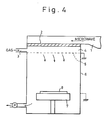
- FIG. 4 An apparatus for carrying out a downstream ashing method is shown in Fig. 4.
- a vacuum reaction chamber 6 is connected to the vacuum pump P, the reaction gases are fed through the gas introducing inlet 3 into the plasma generation chamber 4 provided in reaction chamber 6, and are then formed into a plasma by, for example, microwaves at a frequency of, for example, 2.45 GHz, transmitted through a microwave transmission window 2 by a waveguide 1.
- the ions and the electrons are shielded by the earthed shower head 5, and residual (neutral) active species pass through the shower head 5 and flow down toward the wafer 8 on the stage 7.
- the active species come into contact with the wafer 8 and remove the resist film, comprising an organic material (not shown) coated on the wafer 8, by ashing.
- a gas composed mainly of oxygen is introduced, as the gas for ashing, through the gas introducing inlet 3, formed into a plasma, and subjected to a downstream to bring the active species of oxygen atoms into contact with the wafer 8.
- the activation energy during the ashing is as high as 0.52 eV, the influence on the ashing rate of the temperature (i.e., temperature dependency) is great, and thus the reproducibility and controllability of the ashing are poor.
- the ashing rate is as low as 0.2 ⁇ m/min., and therefore, to obtaining the minimum limit of an about 0.5 ⁇ m/min. of ashing rate required for practical application, the wafer 8 must be heated to about 200°C or higher, and accordingly, the contamination problems of the wafer 8 arises.
- This method may be carried out using the apparatus of Fig. 4, by introducing O2 and H2O through the gas introducing inlet 3 to form the same into a plasma, which is then subjected to a downstream to bring active species of oxygen atoms formed from oxygen, oxygen atoms, and hydrogen atoms and OH formed from H2O, into contact with the wafer 8.
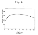
- Fig. 6 the relationship between the ratio of H2O to the total amount of the gas mixture of O2 and H2O is shown in Fig. 6. It should be noted that the stage temperature is 180°C, and the flow rate of the gas mixture of O2 and H2O is 1 liter/min.
- the ashing rate reaches a maximum value of 0.35 ⁇ m/min., which is about 2-fold that of the ashing method using a gas composed mainly of oxygen, when the content of H2O is 30% to 40%. Even when the ratio of H2O is further increased, the ashing rate is not substantially lowered.
- the activation energy is less, at 0.39 eV, compared with the ashing method using a gas composed mainly of oxygen. This is considered to be due to a lowering of the activation energy by OH formed primarily from H2O.
- the temperature dependency is reduced, and thus the reproducibility and controllability are improved.
- the wafer 8 must be heated to about 200°C or higher, and thus the contamination problems of the wafer still remains.
- an ashing rate of 1 ⁇ m/min. or higher which is about 5-fold higher than that of the method using a gas composed mainly of oxygen, can be obtained when about 10% to 15% of a gas containing a small amount of halogen, for example, carbon tetrafluoride (CF4) in oxygen, is added to the plasma.
- a gas containing a small amount of halogen for example, carbon tetrafluoride (CF4) in oxygen
- the gas containing a halogen promotes the dissociation of oxygen into oxygen atoms, when the gas containing oxygen and a halogen is formed into a plasma.
- the active species of oxygen atoms are increased, to improve the ashing rate, and at the same time, ashing at room temperature is possible due to a lowering of the activation energy by the action of fluorine, and further, an additional advantage is gained in that the temperature dependency is greatly reduced.
- the fluorine atoms reach the SiO2 surface, a drawback arises in that the substrate layer of, for example, SiO2, may be etched during the ashing process.
- a further method which can provide a satisfactory ashing rate even at room temperature, performs ashing by using a gas containing mainly fluorine, as described below:
- the method may be carried out in a modified downstream ashing apparatus such as that of Figure 5, which is an improved form of the apparatus of Fig. 4.
- This method comprises injecting NF3 through the gas introducing inlet 3 to form a plasma, and then subjecting the active species of fluorine atoms to a downstream through the shower plate 5.
- H2O is added in an amount smaller than the amount of NF3 injected, whereby the chemical reaction with fluorine and H2O, as shown below, occurs 2 F + H2O ⁇ 2HF + O to generate the oxygen atoms necessary for ashing.
- residual fluorine atoms which have not undergone the chemical reaction withdraw H from the C-H bond on the resist surface, thereby substituting for the H (H. Okano et al. The Electrochem. Soc. Spring Meeting, Atlanta, May 15 - 20, 1988).
- the ashing rate is improved by the oxygen atoms formed by the chemical reaction between the H2O and fluorine atoms, and the residual fluorine atoms, which have not undergone the chemical reaction. Further, the activation energy is lowered by a substitution of H from the C-H bond on the resist surface with fluorine atom, and accordingly, in addition to enabling ashing at room temperature, an advantage is gained in that the temperature dependency is greatly reduced.
- the wafer temperature In the first method described above, in which a gas composed mainly of oxygen is used, and in the method (a) (downstream ashing method with oxygen and water), the wafer temperature must be raised to 200°C or higher, to obtain a practical ashing rate, and thus the problem of wafer contamination can arise.
- a halogen-containing gas namely (b) the method of using a gas containing oxygen and a halogen, and (c) the method of adding water during the downstream of nitrogen trifluoride (NF3), because fluorine, which is a gas containing a halogen, is used to obtain a practical ashing rate even at room temperature, a problem can arise in that the substrate layer of, for example, SiO2, is etched.
- NF3 nitrogen trifluoride
- the above-described methods may not provide a satisfactory ashing rate at low temperature without etching the substrate layer, and without generating a contamination of the wafer.
- the substrate layer e.g. silicon dioxide, silicon nitride
- the substrate layer e.g. silicon dioxide, silicon nitride
- An embodiment of the present invention can provide a process for stripping an organic material, which comprises forming gases including a gas containing oxygen and a gas containing a halogen into plasma in a plasma chamber, and supplying an active species in the gas formed plasma to a reaction chamber to strip the organic material in the reaction chamber, wherein an amount of water vapor of at least one mole based upon two moles of the dissociated halogen atom is fed into the reaction chamber, and the active species of the halogen are removed before contact thereof with the organic material.
- the gas containing the halogen promotes dissociation of oxygen into free oxygen atoms, to increase the amount of free oxygen atoms.
- oxygen-containing gas are oxygen; air, and a mixture of oxygen with an inert gas, CO2 and /or N2.
- halogen-containing gas examples include F2, Cl2, Br2, HF, CF4, NF3, C2F6, C3F8, CHF3, SF6, CCl4, ClF3 , CCl2F2, C2ClF5, C2Cl2F4, CClF3 and Hbr, CBrF3, and xenon fluoride.
- the use of a fluorine-containing gas is preferable.
- the molar ratio of the halogen-containing gas/(the halogen-containing gas + the oxygen-containing gas) is preferably 0.05 to 0.3, more preferably 0.1 to 0.25.
- the active species in the gas formed into plasma are supplied to the vacuum reaction chamber 6, and water vapor is added in an amount of at least one mole, preferably 1.2 to 2.4 moles, for every 2 moles of the dissociated halogen atom (i.e., active species), during the course of the downward flow of the active species, the following chemical reaction occurs: 2 X + H2O ⁇ 2 HX + O.
- the active species of halogen formed by the halogen-containing gas which is utilized to promote a dissociation of oxygen, are substantially completely removed, and therefore, the substrate layer (e.g., SiO2, SiN) is not significantly etched.
- a part of the added water vapor is separated into oxygen atoms, hydrogen atoms, and OH by a secondary reaction with the active species in the downstream, to thereby increase the active species, and as a result, the amount of oxygen atoms and other active species participating in the ashing is increased, and thus the ashing rate is improved.
- the activation energy is lowered by the OH generated by the secondary reaction, whereby ashing at a lower temperature becomes possible, and further, the temperature dependency is reduced to thereby improve the reproducibility and controllability.
- the water vapor can be introduced into the reaction chamber by evacuating the content of a water vessel containing water.
- the water vessel can be optionally heated by a heater (e.g. an electric heater).
- the water vapor can also be introduced into the reaction chamber by bubbling the water in the water vessel with an inert carrier gas (e.g., N2, O2, H2, Ar, He).
- an inert carrier gas e.g., N2, O2, H2, Ar, He.
- a silicon wafer 8 having a diameter of 4 inches (about 10 cm) was used as the substrate of the sample to be ashed, a silicon wafer 8 having a diameter of 4 inches (about 10 cm) was used, a substrate layer of SiO2 is formed on the surface of the wafer 8 by the thermal oxidation method, and a resist of OFPR 800 (i.e., cresol-novolak resin type positive photoresist, a product of Tokyo Ohka K.K.), was then coated thereon by the spin coating method.
- OFPR 800 i.e., cresol-novolak resin type positive photoresist, a product of Tokyo Ohka K.K.
- the ashing process was carried out in the apparatus of Fig. 5, which has a plurality of water vapor inlets 9 capable of supplying water to be uniformly added to the reaction chamber 6, and the amounts of water supplied through the water vapor inlets 9 can be controlled.
- the other arrangements are similar to those as shown in Fig. 4.
- the pressure in the reaction vessel 6 is maintained at usually 0.1 to 3 Torr, typically about 0.8 Torr, and a microwave having a frequency of, for example, 2.45 GHz generated from a microwave generating device 11 is transmitted by a waveguide 1.
- a radio frequency can also be used instread of the microwave.
- gases for the ashing for example, oxygen and a small amount of CF4, introduced through the gas introducing inlet 3 from the bombs 12 and 13 through a mass flow controller 14, are used, and water in a saturated vapor preessure state is supplied through the water vapor inlet 9.
- the total amount of oxygen, CF4, and water at this time is controlled to one liter/min.
- the water vapor can be introduced by evacuating a water vessel 15 containing water 16 via a mass flow controller 14 or by bubbling an inert gas (e.g., N2) from a gas bomb or cylinder 18 via a mass flow controller 14.
- the water vessel 15 can be appropriately heated by a heater 17.
- the gases formed into a plasma are given a constant ratio of an amount of CF4 of 15% relative to the amount of a gas mixture of the oxygen and CF4.
- the change in the SiO2 etching rate was determined when the added amount of water was varied from 0 to 30%.
- a sample having SiO2 formed on the whole surface of the wafer 8 as described above was used.
- the sample was mounted on a stage 7 having a temperature of 150°C, ashing was performed for 10 minutes, a measurement was conducted after ashing by a known esoprimetric method, and the SiO2 etching rate was obtained from the result of that measurement.
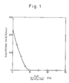
- the minimum limit of this measurement method is 5 ⁇ . The results are shown in Fig. 1.
- axis of the ordinate depicts the SiO2 etching rate
- the axis of the abscissa depicts the ratio of water relative to the total amount of oxygen, CF4, and water.
- the SiO2 When water was not added, the SiO2 was etched at an etching rate of about 230 ⁇ . As the added amount of water was increased, the etching rate was gradually lowered, and no etching of the SiO2 occurred when the added amount of water was more than about 10%.
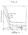
- a wafer 8 having a resist coated to a thickness of 1.1 ⁇ m on the surface thereof was used as the sample. After ashing of the sample for 30 seconds, the thickness of the resist was measured by a contact needle type step difference measuring instrument, and the ashing rate of the resist was calculated.
- axis of the ordinate depicts the ashing rate of the resist
- the axis of the abscissa depicts the ratio of water to the total amount of oxygen, CF4, and water.
- the ashing rate was very high, at 1 ⁇ m/min. or more, even when the temperature of the stage 7 was at room temperature, and thereafter, as the added amount of water was increased to about 10%, the ashing rate was lowered.
- the added amount of water exceeded about 10%, the ashing rate of a wafer at room temperature could not be measured, and the ashing rate became about 0.5 ⁇ m/min. and about 0.9 ⁇ m/min., at wafer temperatures of 150°C, and 180°C, respectively.
- the ashing rate which is about 0.9 ⁇ m/min. at a wafer temperature of 180°C, is lower than when the added amount of water is less than about 10%
- the ashing rate is improved about 5-fold compared with the method described above in which a gas composed mainly of oxygen is used, and about 2.5-fold compared with the method in which O2 + H2O are used as shown in Figure 4.
- the ashing rate is smaller when the added amount of water is about 10% or more than when it is smaller than about 10%. This may be considered to be due to an increased activation energy caused by the removal of fluorine atoms, and this can be readily estimated also from the tendency toward a change of the SiO2 etching rate shown in Fig. 1 with the added amount of water of 10% as the boundary, which is the same as the ashing rate tendency shown in the Fig. 1.
- the active species amount of oxygen atoms is increased by a generation of secondary oxygen atoms through the chemical reaction between water and fluorine, and further, oxygen atoms through the oxygen dissociation action of fluorine, and oxygen atoms and other active species through the secondary reaction can be obtained, the ashing rate is improved compared with the method in which O2 + H2O are used.
- the activation energy at this time was determined as described below.
- a wafer 8 surface coated with a resist to a thickness of 1.1 ⁇ m was used as the sample.
- the sample was mounted on the stage, and after ashing was performed by varying the stage temperature at predetermined temperature intervals each time the added amount of water was varied, the thickness of the resist was measured by a contact needle type step difference measuring instrument, and the ashing rate of the resist was calculated.
- the activation energy was determined from the slope of the straight line.
- the Fig. 3 the activation energy is shown on the logarithmic scale on the axis of the ordinate, and the ratio of water relative to the total amount of oxygen, CF4, and water on the axis of the abscissa.
- the activation energy was as low as 0.05 eV, due to the influence of the fluorine atoms. Subsequently, as the added amount of water was increased to about 10%, the activation energy became higher, until at about 10% or higher, the activation energy became stabilized at about 0.39 eV, as in the downstream ashing method in which oxygen and water were used.
- This phenomenon is understood to be due to the fact that, if the added amount of water is about 10% or more, fluorine atoms can be removed to eliminate the influence of the fluorine, whereby OH formed from water by a secondary reaction mainly determines the activation energy.
- water is added in an amount larger than that of the active species of fluorine atoms. That is, when the ratio of CF4 relative to the amount of the gas mixture of oxygen and CF4 is 15%, ashing is performed with the added amount of water of about 10% or more.
- OH formed by a separation of water lowers the activation energy to 0.39 eV, which is less than the 0.52 eV obtained in the method described above in which a gas composed mainly of oxygen is used, and thus in addition to enabling ashing at a lower temperature, the temperature dependency is reduced and the reproducibility and controllability are accordingly enhanced.
- the ashing rate was about 10,000 ⁇ /min.
- the ashing rate was about 7,500 ⁇ /min. Thus, about 33% increase in the ashing rate was attained by the above process embodying the invention.
- the process in this Example is not limited to the ashing of a resist, but also can be applied to the oxidation and ashing of a large number of organic materials other than a resist.
- CF4 was employed as the gas for ashing, similar effects can be obtained even when the other fluorine-containing gases (e.g., C2F6 and NF3), which are fluorinated gases, are employed, and a gas containing a halogen also may be used.
- the number of oxygen atoms participating in the ashing can be increased and substantially all halogen atoms are removed before they reach the wafer, and further, the reproducibility and controllability are enhanced by lowering the activation energy to thereby reduce the temperature dependency. Accordingly, a high ashing rate can be achieved at a desirably low temperature, without unacceptable etching of the substrate layer, thereby assisting in the production of substantially undamaged semiconductor devices.
Landscapes
- Engineering & Computer Science (AREA)
- Physics & Mathematics (AREA)
- General Physics & Mathematics (AREA)
- Computer Hardware Design (AREA)
- Condensed Matter Physics & Semiconductors (AREA)
- Manufacturing & Machinery (AREA)
- Microelectronics & Electronic Packaging (AREA)
- Power Engineering (AREA)
- Chemical & Material Sciences (AREA)
- Chemical Kinetics & Catalysis (AREA)
- General Chemical & Material Sciences (AREA)
- Plasma & Fusion (AREA)
- Drying Of Semiconductors (AREA)
- Exposure Of Semiconductors, Excluding Electron Or Ion Beam Exposure (AREA)
Abstract
Description
- The present invention relates to methods of stripping organic material, for example, to remove a resist such as a photoresist, X-ray resist, or electron beam resist, used in the production of semiconductor devices, liquid crystal devices and plasma displays.
- In the production of semiconductor devices, usually a photoresist (hereinafter abbreviated as resist) is used as a mask when etching a wafer, and as the resist becomes unnecessary after the etching treatment, it must be removed. The removal methods include the wet treatment system in which a resist stripping solution is used, and the dry treatment system of oxydizing or ashing the resist in an active species of oxygen atoms or an oxygen plasma.
- Currently, dry treatments, which comprise simple ashing steps but can also treat the resist carbonized in the process of ion injection, are widely used, and among these treatments, the downstream ashing method, which causes little or no damage to the wafer, is most widely used.
- In one form of dry treatment utilizing the downstream ashing method, a gas composed mainly of oxygen gas is used for the ashing is Nevertheless, since the ashing rate (i.e., amount of organic material per unit of time) is low, the wafer must be heated to about 200°C or higher to obtain a satisfactory ashing rate. When the wafer is thus heated, however, a minute amount of heavy metals and alkaline metals contained in the resist is introduced into the wafer, whereby problems relating to contamination of the wafer can arise.
- Accordingly, the development of a technique by which a satisfactory ashing rate can be obtained at a low temperature, at which contamination of the wafer does not occur, is desirable.
- An apparatus for carrying out a downstream ashing method is shown in Fig. 4.
- As shown in Fig. 4, a
vacuum reaction chamber 6 is connected to the vacuum pump P, the reaction gases are fed through thegas introducing inlet 3 into theplasma generation chamber 4 provided inreaction chamber 6, and are then formed into a plasma by, for example, microwaves at a frequency of, for example, 2.45 GHz, transmitted through amicrowave transmission window 2 by awaveguide 1. - Among the ions, electrons, and active species formed by plasma formation, the ions and the electrons are shielded by the
earthed shower head 5, and residual (neutral) active species pass through theshower head 5 and flow down toward thewafer 8 on thestage 7. The active species come into contact with thewafer 8 and remove the resist film, comprising an organic material (not shown) coated on thewafer 8, by ashing. - In the downstream ashing method of Fig. 4, a gas composed mainly of oxygen is introduced, as the gas for ashing, through the
gas introducing inlet 3, formed into a plasma, and subjected to a downstream to bring the active species of oxygen atoms into contact with thewafer 8. - According to this method, since the activation energy during the ashing is as high as 0.52 eV, the influence on the ashing rate of the temperature (i.e., temperature dependency) is great, and thus the reproducibility and controllability of the ashing are poor. Further, when the stage temperature is 180°C, the ashing rate is as low as 0.2 µm/min., and therefore, to obtaining the minimum limit of an about 0.5 µm/min. of ashing rate required for practical application, the
wafer 8 must be heated to about 200°C or higher, and accordingly, the contamination problems of thewafer 8 arises. - To enable ashing to be carried out at a lower temperature than that used in the above-described downstream method, the following methods may be used:
- This method may be carried out using the apparatus of Fig. 4, by introducing O₂ and H₂O through the
gas introducing inlet 3 to form the same into a plasma, which is then subjected to a downstream to bring active species of oxygen atoms formed from oxygen, oxygen atoms, and hydrogen atoms and OH formed from H₂O, into contact with thewafer 8. - In this method, the relationship between the ratio of H₂O to the total amount of the gas mixture of O₂ and H₂O is shown in Fig. 6. It should be noted that the stage temperature is 180°C, and the flow rate of the gas mixture of O₂ and H₂O is 1 liter/min.
- As seen from the Fig. 6, when the ratio of H₂O is increased, the ashing rate reaches a maximum value of 0.35 µm/min., which is about 2-fold that of the ashing method using a gas composed mainly of oxygen, when the content of H₂O is 30% to 40%. Even when the ratio of H₂O is further increased, the ashing rate is not substantially lowered.
- This is considered to be because the oxygen atoms formed from H₂O and other active species participate in the ashing, together with the oxygen atoms formed from oxygen.
- Also, the activation energy is less, at 0.39 eV, compared with the ashing method using a gas composed mainly of oxygen. This is considered to be due to a lowering of the activation energy by OH formed primarily from H₂O.
- As the result, in addition to enabling ashing at a temperature lower than that used in the ashing method using a gas composed mainly of oxygen, the temperature dependency is reduced, and thus the reproducibility and controllability are improved. To obtain a practical ashing rate, however, the
wafer 8 must be heated to about 200°C or higher, and thus the contamination problems of the wafer still remains. - It is found that when using a gas composed mainly of oxygen, a satisfactory ashing rate can be obtained at a low temperature by an addition of a fluorine gas, as described below:
- It is found in use of the Fig. 4 apparatus that an ashing rate of 1 µm/min. or higher, which is about 5-fold higher than that of the method using a gas composed mainly of oxygen, can be obtained when about 10% to 15% of a gas containing a small amount of halogen, for example, carbon tetrafluoride (CF₄) in oxygen, is added to the plasma.
- This is because the gas containing a halogen promotes the dissociation of oxygen into oxygen atoms, when the gas containing oxygen and a halogen is formed into a plasma.
- Further, when even a small amount of a gas containing fluorine, as a halogen, is added, and the active species of the fluorine come into contact with the
wafer 8, the activation energy during ashing is remarkably lowered to about 0.05 eV, compared with the method using only oxygen (V. Vukanovic et al., J. vac. Sci. Technol., B6 (1), Jan/Feb 1988 pp. 66, J.M. Cook and Brent W. Benson, J. Electrochem. Soc. Vol., 130, No. 12, December, 1983, pp. 2459) - In this method, the active species of oxygen atoms are increased, to improve the ashing rate, and at the same time, ashing at room temperature is possible due to a lowering of the activation energy by the action of fluorine, and further, an additional advantage is gained in that the temperature dependency is greatly reduced. Nevertheless, when the fluorine atoms reach the SiO₂ surface, a drawback arises in that the substrate layer of, for example, SiO₂, may be etched during the ashing process.
- A further method, which can provide a satisfactory ashing rate even at room temperature, performs ashing by using a gas containing mainly fluorine, as described below:
- The method may be carried out in a modified downstream ashing apparatus such as that of Figure 5, which is an improved form of the apparatus of Fig. 4.
- This method comprises injecting NF₃ through the
gas introducing inlet 3 to form a plasma, and then subjecting the active species of fluorine atoms to a downstream through theshower plate 5. During the downstream from theaddition inlet 9, H₂O is added in an amount smaller than the amount of NF₃ injected, whereby the chemical reaction with fluorine and H₂O, as shown below, occurs
2 F + H₂O → 2HF + O
to generate the oxygen atoms necessary for ashing. Also, residual fluorine atoms which have not undergone the chemical reaction withdraw H from the C-H bond on the resist surface, thereby substituting for the H (H. Okano et al. The Electrochem. Soc. Spring Meeting, Atlanta, May 15 - 20, 1988). - According to this method, the ashing rate is improved by the oxygen atoms formed by the chemical reaction between the H₂O and fluorine atoms, and the residual fluorine atoms, which have not undergone the chemical reaction. Further, the activation energy is lowered by a substitution of H from the C-H bond on the resist surface with fluorine atom, and accordingly, in addition to enabling ashing at room temperature, an advantage is gained in that the temperature dependency is greatly reduced.
- Nevertheless, because fluorine atoms reach the surface of the
wafer 8, the problem of an etching of the substrate layer such as SiO₂ arises, and further, because oxygen atoms are obtained by an exothermic reaction between fluorine atoms and H₂O, the wafer surface is heated by excess heat radiated therefrom, whereby the contamination problems of thewafer 8 with, for example, heavy metals, arises. - In the first method described above, in which a gas composed mainly of oxygen is used, and in the method (a) (downstream ashing method with oxygen and water), the wafer temperature must be raised to 200°C or higher, to obtain a practical ashing rate, and thus the problem of wafer contamination can arise.
- In the methods of using a halogen-containing gas, namely (b) the method of using a gas containing oxygen and a halogen, and (c) the method of adding water during the downstream of nitrogen trifluoride (NF₃), because fluorine, which is a gas containing a halogen, is used to obtain a practical ashing rate even at room temperature, a problem can arise in that the substrate layer of, for example, SiO₂, is etched.
- Further, in the downstream ashing method of (c), because the chemical reaction between water and fluorine atoms is an exothermic reaction, and therefore, the wafer surface is excessively heated, the above-mentioned contamination problems of the wafer can arise.
- Accordingly, the above-described methods may not provide a satisfactory ashing rate at low temperature without etching the substrate layer, and without generating a contamination of the wafer.
- Recently, the present inventors briefly reported a possibility of a downstream ashing method using O₂, CF₄, and H₂O as an ashing gas in Extended Abstracts of the 49 th Autumn Meetings, 1988; The Japan Society of Applied Physics page 553 (October, 1988). This method is disclosed in a copending U.S. Patent Application Serial No. 361178 filed June 5, 1989.
- It is therefore desirable to provide a method of stripping an organic material by which the substrate layer (e.g. silicon dioxide, silicon nitride) is not etched, a satisfactory ashing rate at a desirably low temperature is obtained, and the semiconductor elements or other devices concerned are not unacceptably damaged.
- It is also desirable to provide an apparatus for carrying out such a method.
- An embodiment of the present invention can provide a process for stripping an organic material, which comprises forming gases including a gas containing oxygen and a gas containing a halogen into plasma in a plasma chamber, and supplying an active species in the gas formed plasma to a reaction chamber to strip the organic material in the reaction chamber, wherein an amount of water vapor of at least one mole based upon two moles of the dissociated halogen atom is fed into the reaction chamber, and the active species of the halogen are removed before contact thereof with the organic material. Reference will now be made, by way of example, to the accompanying drawings, wherein:
- Figure 1 is a graph showing the relationship between the added amount of water and the SiO₂ etching rate in a process embodying the present invention;
- Figure 2 is a graph showing the relationship between the added amount of water relative to the temperature of the wafer in a process embodying the present invention;
- Figure 3 is a graph showing the relationship between the added amount of water vapor and the activation energy in a process embodying the present invention;
- Fig. 4 is an illustration showing a downstream ashing apparatus;
- Fig. 5 is an illustration showing a further downstream ashing apparatus; and,
- Fig. 6 is a graph showing the relationship between the added amount of water and the ashing rate of the resist in in a previously-considered downstream ashing method using oxygen and water.
- A process for ashing an organic material embodying the present invention is described below.
- By forming gases, including a gas containing oxygen and a gas containing a small amount of a halogen, into plasma in the plasma chamber 4 (see Fig. 5), the gas containing the halogen promotes dissociation of oxygen into free oxygen atoms, to increase the amount of free oxygen atoms. Examples of oxygen-containing gas are oxygen; air, and a mixture of oxygen with an inert gas, CO₂ and /or N₂. Examples of the halogen-containing gas are F₂, Cl₂, Br₂, HF, CF₄, NF₃, C₂F₆, C₃F₈, CHF₃, SF₆, CCl₄, ClF₃ , CCl₂F₂, C₂ClF₅, C₂Cl₂F₄, CClF₃ and Hbr, CBrF₃, and xenon fluoride. The use of a fluorine-containing gas is preferable.
- The molar ratio of the halogen-containing gas/(the halogen-containing gas + the oxygen-containing gas) is preferably 0.05 to 0.3, more preferably 0.1 to 0.25.
- When the active species in the gas formed into plasma are supplied to the
vacuum reaction chamber 6, and water vapor is added in an amount of at least one mole, preferably 1.2 to 2.4 moles, for every 2 moles of the dissociated halogen atom (i.e., active species), during the course of the downward flow of the active species, the following chemical reaction occurs:
2 X + H₂O → 2 HX + O.
By utilizing this chemical reaction, the active species of halogen formed by the halogen-containing gas, which is utilized to promote a dissociation of oxygen, are substantially completely removed, and therefore, the substrate layer (e.g., SiO₂, SiN) is not significantly etched. - Also, a part of the added water vapor is separated into oxygen atoms, hydrogen atoms, and OH by a secondary reaction with the active species in the downstream, to thereby increase the active species, and as a result, the amount of oxygen atoms and other active species participating in the ashing is increased, and thus the ashing rate is improved.
- Further, when the active species come into contact with the organic material, to effect ashing, the activation energy is lowered by the OH generated by the secondary reaction, whereby ashing at a lower temperature becomes possible, and further, the temperature dependency is reduced to thereby improve the reproducibility and controllability.
- Although the chemical reaction between water and atoms of a halogen is an exothermic reaction, only a small amount of the gas containing a halogen need be used, because it is utilized for the dissociation of oxygen, whereby the amount of heat generated is reduced to an extent such that it does not affect the wafer.
- The water vapor can be introduced into the reaction chamber by evacuating the content of a water vessel containing water. The water vessel can be optionally heated by a heater (e.g. an electric heater). The water vapor can also be introduced into the reaction chamber by bubbling the water in the water vessel with an inert carrier gas (e.g., N₂, O₂, H₂, Ar, He).
- The above-discussed process for ashing organic material will now be illustrated by reference to Examples which utilize the downstream ashing process for the ashing of a resist coated on the surface of a wafer.
- In these Examples (see Fig. 5), as the substrate of the sample to be ashed, a
silicon wafer 8 having a diameter of 4 inches (about 10 cm) was used, a substrate layer of SiO₂ is formed on the surface of thewafer 8 by the thermal oxidation method, and a resist of OFPR 800 (i.e., cresol-novolak resin type positive photoresist, a product of Tokyo Ohka K.K.), was then coated thereon by the spin coating method. - The ashing process was carried out in the apparatus of Fig. 5, which has a plurality of
water vapor inlets 9 capable of supplying water to be uniformly added to thereaction chamber 6, and the amounts of water supplied through thewater vapor inlets 9 can be controlled. The other arrangements are similar to those as shown in Fig. 4. - The ashing conditions when performing ashing by using the apparatus of Fig. 5 are described below.
- The pressure in the
reaction vessel 6 is maintained at usually 0.1 to 3 Torr, typically about 0.8 Torr, and a microwave having a frequency of, for example, 2.45 GHz generated from amicrowave generating device 11 is transmitted by awaveguide 1. A radio frequency can also be used instread of the microwave. As the gases for the ashing, for example, oxygen and a small amount of CF₄, introduced through thegas introducing inlet 3 from thebombs mass flow controller 14, are used, and water in a saturated vapor preessure state is supplied through thewater vapor inlet 9. The total amount of oxygen, CF₄, and water at this time is controlled to one liter/min. The water vapor can be introduced by evacuating awater vessel 15 containing water 16 via amass flow controller 14 or by bubbling an inert gas (e.g., N₂) from a gas bomb orcylinder 18 via amass flow controller 14. Thewater vessel 15 can be appropriately heated by aheater 17. - In this Example, to facilitate the comparison between measured values, the gases formed into a plasma are given a constant ratio of an amount of CF₄ of 15% relative to the amount of a gas mixture of the oxygen and CF₄.
- Under the operating conditions of the Figure 5 apparatus and using the sample as described above, the following measurement was performed.
- First, the change in the SiO₂ etching rate was determined when the added amount of water was varied from 0 to 30%.
- At this time, a sample having SiO₂ formed on the whole surface of the
wafer 8 as described above was used. The sample was mounted on astage 7 having a temperature of 150°C, ashing was performed for 10 minutes, a measurement was conducted after ashing by a known esoprimetric method, and the SiO₂ etching rate was obtained from the result of that measurement. The minimum limit of this measurement method is 5 Å. The results are shown in Fig. 1. - In Fig. 1, the axis of the ordinate depicts the SiO₂ etching rate, and the axis of the abscissa depicts the ratio of water relative to the total amount of oxygen, CF₄, and water.
- When water was not added, the SiO₂ was etched at an etching rate of about 230 Å. As the added amount of water was increased, the etching rate was gradually lowered, and no etching of the SiO₂ occurred when the added amount of water was more than about 10%.
- From this result, it can be seen that, of the reduced active species, only the fluorine atoms participate in the etching of the SiO₂, and accordingly it can be seen that, if the added amount of water is increased to more than about 10%, substantially all of the fluorine atoms are removed before reaching the wafer, whereby no etching of the SiO₂ occurs.
- Next, the ashing rate when setting the temperature of the
stage 7 at room temperature, 150°C, and 180°C, and varying the added amount of water from 0 to 25%, was determined. - At this time, a
wafer 8 having a resist coated to a thickness of 1.1 µm on the surface thereof was used as the sample. After ashing of the sample for 30 seconds, the thickness of the resist was measured by a contact needle type step difference measuring instrument, and the ashing rate of the resist was calculated. - The results are shown in Fig. 2.
- In Fig. 2, the axis of the ordinate depicts the ashing rate of the resist, and the axis of the abscissa depicts the ratio of water to the total amount of oxygen, CF₄, and water.
- When water was not added, the ashing rate was very high, at 1 µm/min. or more, even when the temperature of the
stage 7 was at room temperature, and thereafter, as the added amount of water was increased to about 10%, the ashing rate was lowered. When the added amount of water exceeded about 10%, the ashing rate of a wafer at room temperature could not be measured, and the ashing rate became about 0.5 µm/min. and about 0.9 µm/min., at wafer temperatures of 150°C, and 180°C, respectively. - As a result, when the added amount of water is made about 10% or more, at which etching of the substrate layer does not occur, although the ashing rate, which is about 0.9 µm/min. at a wafer temperature of 180°C, is lower than when the added amount of water is less than about 10%, the ashing rate is improved about 5-fold compared with the method described above in which a gas composed mainly of oxygen is used, and about 2.5-fold compared with the method in which O₂ + H₂O are used as shown in Figure 4.
- The ashing rate is smaller when the added amount of water is about 10% or more than when it is smaller than about 10%. This may be considered to be due to an increased activation energy caused by the removal of fluorine atoms, and this can be readily estimated also from the tendency toward a change of the SiO₂ etching rate shown in Fig. 1 with the added amount of water of 10% as the boundary, which is the same as the ashing rate tendency shown in the Fig. 1.
- Accordingly, since the active species amount of oxygen atoms is increased by a generation of secondary oxygen atoms through the chemical reaction between water and fluorine, and further, oxygen atoms through the oxygen dissociation action of fluorine, and oxygen atoms and other active species through the secondary reaction can be obtained, the ashing rate is improved compared with the method in which O₂ + H₂O are used.
- Next, the change in activation energy was determined when the added amount of water was varied from 0 to 30%.
- The activation energy at this time was determined as described below. A
wafer 8 surface coated with a resist to a thickness of 1.1 µm was used as the sample. The sample was mounted on the stage, and after ashing was performed by varying the stage temperature at predetermined temperature intervals each time the added amount of water was varied, the thickness of the resist was measured by a contact needle type step difference measuring instrument, and the ashing rate of the resist was calculated. By plotting the values on the axis of the ordinate on the logarithmic scale and the absolute temperatures on the axis of the abscissa on a reciprocal number scale, to prepare an Arrhenius plot, the activation energy was determined from the slope of the straight line. - The results are shown in Fig. 3.
- The Fig. 3, the activation energy is shown on the logarithmic scale on the axis of the ordinate, and the ratio of water relative to the total amount of oxygen, CF₄, and water on the axis of the abscissa.
- When water was not added, the activation energy was as low as 0.05 eV, due to the influence of the fluorine atoms. Subsequently, as the added amount of water was increased to about 10%, the activation energy became higher, until at about 10% or higher, the activation energy became stabilized at about 0.39 eV, as in the downstream ashing method in which oxygen and water were used.
- As a result, when the added amount of water was about 10% or more, although the value of the activation energy of about 0.39 eV was greater than when the added amount of water was about 10% or less, as shown in Fig. 3, it became smaller compared with the 0.52 eV obtained in the method described above in which a gas composed mainly of oxygen was used.
- Accordingly, in addition to enabling ashing at a lower temperature than in the latter method using a gas composed mainly of oxygen, the temperature dependency was reduced and thus the reproducibility and controllability were enhanced.
- This phenomenon is understood to be due to the fact that, if the added amount of water is about 10% or more, fluorine atoms can be removed to eliminate the influence of the fluorine, whereby OH formed from water by a secondary reaction mainly determines the activation energy.
- From the above description, in this Example, when ashing of the resist is performed in the state in which the added amount of water is less than about 10%, namely the state in which the added amount of water is smaller than the amount of active species of fluorine atoms, a high ashing rate can be obtained at room temperature. Nevertheless, as shown in Fig. 1, since the SiO₂ substrate layer is etched, which has an adverse influence on the element formed on the
wafer 8, ashing is not performed. - Therefore, in this Example, water is added in an amount larger than that of the active species of fluorine atoms. That is, when the ratio of CF₄ relative to the amount of the gas mixture of oxygen and CF₄ is 15%, ashing is performed with the added amount of water of about 10% or more. Accordingly, since all fluorine atoms are removed by the H₂O added during the course of the downstream, before reaching the wafer, no etching of the substrate layer by fluorine atoms occurs, and further, due to the oxygen atoms obtained by the oxygen dissociation action of fluorine, the oxygen atoms generated by the chemical reaction of fluorine and water, and the oxygen atoms formed by the secondary reaction, the number of oxygen atoms can be increased, and therefore, when the stage temperature is 180°C, the ashing rate can be greatly improved to about 5-fold that of the method using a gas composed mainly of oxygen, and about 2.5-fold that of the method using oxygen and water.
- Also, OH formed by a separation of water lowers the activation energy to 0.39 eV, which is less than the 0.52 eV obtained in the method described above in which a gas composed mainly of oxygen is used, and thus in addition to enabling ashing at a lower temperature, the temperature dependency is reduced and the reproducibility and controllability are accordingly enhanced.
- As comparative tests, the following experiments were effected. First, in a process embodying the present invention, the above-mentioned resist ashing was carried out under the following conditions:
CF₄ / (O₂ + CF₄) = 15%
O₂ + CF₄ = 1 liter/min.
Water vapor = about 200 ml/min.
Microwave = 1.5 KW
Vacuum of reaction chamber = 0.8 Torr
Wafer Temperature = 160°C - The ashing rate was about 10,000 Å/min.
- As a Comparative Example, the water vapor was fed to the plasma chamber, together with CF₄ and O₂, under the following conditions. The other conditions were the same as above.
O₂ + CF₄ + H₂O = 1 liter/min.
CF₄ / O₂ = 15%
H₂O = about 100 cc/min. - The ashing rate was about 7,500 Å/min. Thus, about 33% increase in the ashing rate was attained by the above process embodying the invention.
- The process in this Example is not limited to the ashing of a resist, but also can be applied to the oxidation and ashing of a large number of organic materials other than a resist. Also, although CF₄ was employed as the gas for ashing, similar effects can be obtained even when the other fluorine-containing gases (e.g., C₂F₆ and NF₃), which are fluorinated gases, are employed, and a gas containing a halogen also may be used.
- As described above, in a process embodying the invention, the number of oxygen atoms participating in the ashing can be increased and substantially all halogen atoms are removed before they reach the wafer, and further, the reproducibility and controllability are enhanced by lowering the activation energy to thereby reduce the temperature dependency. Accordingly, a high ashing rate can be achieved at a desirably low temperature, without unacceptable etching of the substrate layer, thereby assisting in the production of substantially undamaged semiconductor devices.
Claims (16)
characterised in that water vapour is introduced into the said working chamber at a rate such that the working chamber receives at least one mole of water vapour for every two moles of free halogen atoms received therein from the plasma chamber, thereby to prevent such free halogen atoms from contacting the said organic film.
supplying an active species of the halogen in said gas formed plasma to a reaction chamber to strip the organic material in said reaction chamber, wherein at least one mole of water vapor based upon two moles of the dissociated halogen atom is introduced into said reaction chamber, and
said active species of the halogen are removed before contact thereof with said organic material.
a reaction chamber provided with a stage for placing the organic material to be treated; a plasma generating means; a gas introducing inlet; a shower head; a water vapor inlet means; and a gas evacuating conduit.
Applications Claiming Priority (2)
| Application Number | Priority Date | Filing Date | Title |
|---|---|---|---|
| JP1003303A JP2890432B2 (en) | 1989-01-10 | 1989-01-10 | Ashing method of organic matter |
| JP3303/89 | 1989-01-10 |
Publications (2)
| Publication Number | Publication Date |
|---|---|
| EP0379301A1 true EP0379301A1 (en) | 1990-07-25 |
| EP0379301B1 EP0379301B1 (en) | 1995-11-08 |
Family
ID=11553594
Family Applications (1)
| Application Number | Title | Priority Date | Filing Date |
|---|---|---|---|
| EP90300282A Expired - Lifetime EP0379301B1 (en) | 1989-01-10 | 1990-01-10 | Method of stripping organic material |
Country Status (5)
| Country | Link |
|---|---|
| US (1) | US4983254A (en) |
| EP (1) | EP0379301B1 (en) |
| JP (1) | JP2890432B2 (en) |
| KR (1) | KR940001646B1 (en) |
| DE (1) | DE69023355D1 (en) |
Cited By (8)
| Publication number | Priority date | Publication date | Assignee | Title |
|---|---|---|---|---|
| WO1991001516A2 (en) * | 1989-07-21 | 1991-02-07 | Board Of Regents, The University Of Texas System | Pattern forming and transferring processes |
| WO1993015444A1 (en) * | 1992-01-30 | 1993-08-05 | Fraunhofer-Gesellschaft zur Förderung der angewandten Forschung e.V. | Method for the dry development of a silicon-containing lacquer film sensitive to uv and/or electron-beam radiation |
| WO1995022171A2 (en) * | 1994-02-03 | 1995-08-17 | Applied Materials, Inc. | Stripping, passivation and corrosion inhibition of semiconductor substrates |
| US5545289A (en) * | 1994-02-03 | 1996-08-13 | Applied Materials, Inc. | Passivating, stripping and corrosion inhibition of semiconductor substrates |
| EP0798767A2 (en) * | 1996-03-29 | 1997-10-01 | Praxair Technology, Inc. | Removal of carbon from substrate surface |
| EP0940846A1 (en) * | 1998-03-06 | 1999-09-08 | Interuniversitair Micro-Elektronica Centrum Vzw | Method for stripping ion implanted photoresist layer |
| US6440864B1 (en) | 2000-06-30 | 2002-08-27 | Applied Materials Inc. | Substrate cleaning process |
| US6692903B2 (en) | 2000-12-13 | 2004-02-17 | Applied Materials, Inc | Substrate cleaning apparatus and method |
Families Citing this family (43)
| Publication number | Priority date | Publication date | Assignee | Title |
|---|---|---|---|---|
| JPH0777211B2 (en) * | 1987-08-19 | 1995-08-16 | 富士通株式会社 | Ashing method |
| US5226056A (en) * | 1989-01-10 | 1993-07-06 | Nihon Shinku Gijutsu Kabushiki Kaisha | Plasma ashing method and apparatus therefor |
| EP0416774B1 (en) | 1989-08-28 | 2000-11-15 | Hitachi, Ltd. | A method of treating a sample of aluminium-containing material |
| US5228052A (en) * | 1991-09-11 | 1993-07-13 | Nihon Shinku Gijutsu Kabushiki Kaisha | Plasma ashing apparatus |
| DE4132559A1 (en) * | 1991-09-30 | 1993-04-08 | Siemens Ag | Plasma etching in-situ cleaning process for vacuum deposition chambers - with separate plasma discharge excitation of etch gas and admission of activated etch gas to chamber |
| DE4202158C1 (en) * | 1992-01-27 | 1993-07-22 | Siemens Ag, 8000 Muenchen, De | |
| DE69320963T2 (en) * | 1992-06-22 | 1999-05-12 | Lam Res Corp | PLASMA CLEANING METHOD FOR REMOVING RESIDUES IN A PLASMA TREATMENT CHAMBER |
| US5387289A (en) * | 1992-09-22 | 1995-02-07 | Genus, Inc. | Film uniformity by selective pressure gradient control |
| JP3231426B2 (en) * | 1992-10-28 | 2001-11-19 | 富士通株式会社 | Hydrogen plasma downflow processing method and hydrogen plasma downflow processing apparatus |
| US5445679A (en) * | 1992-12-23 | 1995-08-29 | Memc Electronic Materials, Inc. | Cleaning of polycrystalline silicon for charging into a Czochralski growing process |
| DE4308990A1 (en) * | 1993-03-20 | 1994-09-22 | Bosch Gmbh Robert | Etching method and device for cleaning semiconductor elements, in particular power diodes |
| JPH06285868A (en) * | 1993-03-30 | 1994-10-11 | Bridgestone Corp | Cleaning method of vulcanizing mold |
| JP2804700B2 (en) * | 1993-03-31 | 1998-09-30 | 富士通株式会社 | Semiconductor device manufacturing apparatus and semiconductor device manufacturing method |
| JP3288490B2 (en) * | 1993-07-09 | 2002-06-04 | 富士通株式会社 | Semiconductor device manufacturing method and semiconductor device manufacturing apparatus |
| JP3438109B2 (en) * | 1994-08-12 | 2003-08-18 | 富士通株式会社 | Plasma processing apparatus and plasma processing method |
| JPH08186098A (en) * | 1994-12-27 | 1996-07-16 | Ryoden Semiconductor Syst Eng Kk | Removal of photosensitive resin and removal method |
| US5671116A (en) * | 1995-03-10 | 1997-09-23 | Lam Research Corporation | Multilayered electrostatic chuck and method of manufacture thereof |
| US5753567A (en) * | 1995-08-28 | 1998-05-19 | Memc Electronic Materials, Inc. | Cleaning of metallic contaminants from the surface of polycrystalline silicon with a halogen gas or plasma |
| US5835333A (en) * | 1995-10-30 | 1998-11-10 | Lam Research Corporation | Negative offset bipolar electrostatic chucks |
| US5693147A (en) * | 1995-11-03 | 1997-12-02 | Motorola, Inc. | Method for cleaning a process chamber |
| US5780359A (en) * | 1995-12-11 | 1998-07-14 | Applied Materials, Inc. | Polymer removal from top surfaces and sidewalls of a semiconductor wafer |
| US5812361A (en) * | 1996-03-29 | 1998-09-22 | Lam Research Corporation | Dynamic feedback electrostatic wafer chuck |
| US5614026A (en) * | 1996-03-29 | 1997-03-25 | Lam Research Corporation | Showerhead for uniform distribution of process gas |
| JPH09270421A (en) | 1996-04-01 | 1997-10-14 | Mitsubishi Electric Corp | Surface treatment apparatus and method |
| US6015761A (en) * | 1996-06-26 | 2000-01-18 | Applied Materials, Inc. | Microwave-activated etching of dielectric layers |
| US5925577A (en) * | 1997-02-19 | 1999-07-20 | Vlsi Technology, Inc. | Method for forming via contact hole in a semiconductor device |
| US7001848B1 (en) * | 1997-11-26 | 2006-02-21 | Texas Instruments Incorporated | Hydrogen plasma photoresist strip and polymeric residue cleanup process for oxygen-sensitive materials |
| US6080680A (en) * | 1997-12-19 | 2000-06-27 | Lam Research Corporation | Method and composition for dry etching in semiconductor fabrication |
| US6387819B1 (en) * | 1998-04-29 | 2002-05-14 | Applied Materials, Inc. | Method for etching low K dielectric layers |
| US6410417B1 (en) * | 1998-11-05 | 2002-06-25 | Promos Technologies, Inc. | Method of forming tungsten interconnect and vias without tungsten loss during wet stripping of photoresist polymer |
| US6599829B2 (en) * | 1998-11-25 | 2003-07-29 | Texas Instruments Incorporated | Method for photoresist strip, sidewall polymer removal and passivation for aluminum metallization |
| US6242350B1 (en) | 1999-03-18 | 2001-06-05 | Taiwan Semiconductor Manufacturing Company | Post gate etch cleaning process for self-aligned gate mosfets |
| US6610168B1 (en) * | 1999-08-12 | 2003-08-26 | Sipec Corporation | Resist film removal apparatus and resist film removal method |
| US20050022839A1 (en) * | 1999-10-20 | 2005-02-03 | Savas Stephen E. | Systems and methods for photoresist strip and residue treatment in integrated circuit manufacturing |
| US6805139B1 (en) | 1999-10-20 | 2004-10-19 | Mattson Technology, Inc. | Systems and methods for photoresist strip and residue treatment in integrated circuit manufacturing |
| US6440874B1 (en) * | 2000-03-24 | 2002-08-27 | Advanced Micro Devices, Inc. | High throughput plasma resist strip process for temperature sensitive applications |
| WO2002050883A1 (en) * | 2000-12-18 | 2002-06-27 | Sumitomo Precision Products Co., Ltd | Cleaning method and etching method |
| JP2006019414A (en) * | 2004-06-30 | 2006-01-19 | Canon Inc | Plasma processing device |
| US20070193602A1 (en) * | 2004-07-12 | 2007-08-23 | Savas Stephen E | Systems and Methods for Photoresist Strip and Residue Treatment in Integrated Circuit Manufacturing |
| US20070123049A1 (en) * | 2005-11-17 | 2007-05-31 | Kao-Su Huang | Semiconductor process and method for removing condensed gaseous etchant residues on wafer |
| JP4946321B2 (en) * | 2006-09-29 | 2012-06-06 | 富士通セミコンダクター株式会社 | Substrate processing apparatus and substrate processing method |
| US20080296258A1 (en) * | 2007-02-08 | 2008-12-04 | Elliott David J | Plenum reactor system |
| TWI576938B (en) * | 2012-08-17 | 2017-04-01 | 斯克林集團公司 | Substrate processing apparatus and substrate processing method |
Citations (3)
| Publication number | Priority date | Publication date | Assignee | Title |
|---|---|---|---|---|
| EP0237078A2 (en) * | 1986-03-13 | 1987-09-16 | Fujitsu Limited | Downstream microwave plasma processing apparatus having an improved coupling structure between microwave and plasma |
| EP0328350A2 (en) * | 1988-02-09 | 1989-08-16 | Fujitsu Limited | Dry etching with hydrogen bromide or bromine |
| EP0345757A2 (en) * | 1988-06-09 | 1989-12-13 | Fujitsu Limited | An ashing method for removing an organic film on a substance of a semiconductor device under fabrication |
Family Cites Families (3)
| Publication number | Priority date | Publication date | Assignee | Title |
|---|---|---|---|---|
| US4699689A (en) * | 1985-05-17 | 1987-10-13 | Emergent Technologies Corporation | Method and apparatus for dry processing of substrates |
| US4749440A (en) * | 1985-08-28 | 1988-06-07 | Fsi Corporation | Gaseous process and apparatus for removing films from substrates |
| JPH02174120A (en) * | 1988-12-27 | 1990-07-05 | Toshiba Corp | Removal of organic high-polymer film |
-
1989
- 1989-01-10 JP JP1003303A patent/JP2890432B2/en not_active Expired - Lifetime
-
1990
- 1990-01-04 US US07/460,798 patent/US4983254A/en not_active Expired - Lifetime
- 1990-01-10 KR KR1019900000240A patent/KR940001646B1/en not_active IP Right Cessation
- 1990-01-10 EP EP90300282A patent/EP0379301B1/en not_active Expired - Lifetime
- 1990-01-10 DE DE69023355T patent/DE69023355D1/en not_active Expired - Lifetime
Patent Citations (3)
| Publication number | Priority date | Publication date | Assignee | Title |
|---|---|---|---|---|
| EP0237078A2 (en) * | 1986-03-13 | 1987-09-16 | Fujitsu Limited | Downstream microwave plasma processing apparatus having an improved coupling structure between microwave and plasma |
| EP0328350A2 (en) * | 1988-02-09 | 1989-08-16 | Fujitsu Limited | Dry etching with hydrogen bromide or bromine |
| EP0345757A2 (en) * | 1988-06-09 | 1989-12-13 | Fujitsu Limited | An ashing method for removing an organic film on a substance of a semiconductor device under fabrication |
Non-Patent Citations (5)
| Title |
|---|
| 4EME COLLOQUE INTERNATIONAL SUR LES PLASMAS ET LA PULVERISATION CATHODIQUE, Nice, 13th-17th September 1982, pages 79-87, Paris, FR; G. TURBAN et al.: "Gravure du polyimide kapton H dans les plasmas oxyfluores" * |
| EXTENDED ABSTRACTS/SPRING MEETING, vol. 88-1, 15th-20th May 1988, pages 159-160, Princeton, NY, US; H. OKANO et al.: "Down-flow type resist ashing technique employing reaction of fluorine atoms to water vapor" * |
| PATENT ABSTRACTS OF JAPAN, vol. 13, no. 248 (E-770), 6th June 1989; & JP-A-01 048 421 (FUJITSU LTD) 22-02-1989 * |
| PATENT ABSTRACTS OF JAPAN, vol. 13, no. 268 (E-775), 20th June 1989; & JP-A-01 059 819 (TOKUDO SEISAKUSHO) 07-03-1989 * |
| PATENT ABSTRACTS OF JAPAN, vol. 13, no. 5 (E-701), 9th January 1989; & JP-A-63 217 629 (HITACHI LTD) 09-09-1988 * |
Cited By (13)
| Publication number | Priority date | Publication date | Assignee | Title |
|---|---|---|---|---|
| WO1991001516A2 (en) * | 1989-07-21 | 1991-02-07 | Board Of Regents, The University Of Texas System | Pattern forming and transferring processes |
| WO1991001516A3 (en) * | 1989-07-21 | 1991-04-18 | Univ Texas | Pattern forming and transferring processes |
| US5178989A (en) * | 1989-07-21 | 1993-01-12 | Board Of Regents, The University Of Texas System | Pattern forming and transferring processes |
| WO1993015444A1 (en) * | 1992-01-30 | 1993-08-05 | Fraunhofer-Gesellschaft zur Förderung der angewandten Forschung e.V. | Method for the dry development of a silicon-containing lacquer film sensitive to uv and/or electron-beam radiation |
| US5545289A (en) * | 1994-02-03 | 1996-08-13 | Applied Materials, Inc. | Passivating, stripping and corrosion inhibition of semiconductor substrates |
| WO1995022171A3 (en) * | 1994-02-03 | 1995-09-08 | Applied Materials Inc | Stripping, passivation and corrosion inhibition of semiconductor substrates |
| WO1995022171A2 (en) * | 1994-02-03 | 1995-08-17 | Applied Materials, Inc. | Stripping, passivation and corrosion inhibition of semiconductor substrates |
| EP0798767A2 (en) * | 1996-03-29 | 1997-10-01 | Praxair Technology, Inc. | Removal of carbon from substrate surface |
| EP0798767A3 (en) * | 1996-03-29 | 1998-03-11 | Praxair Technology, Inc. | Removal of carbon from substrate surface |
| US6352936B1 (en) | 1998-02-27 | 2002-03-05 | Imec Vzw | Method for stripping ion implanted photoresist layer |
| EP0940846A1 (en) * | 1998-03-06 | 1999-09-08 | Interuniversitair Micro-Elektronica Centrum Vzw | Method for stripping ion implanted photoresist layer |
| US6440864B1 (en) | 2000-06-30 | 2002-08-27 | Applied Materials Inc. | Substrate cleaning process |
| US6692903B2 (en) | 2000-12-13 | 2004-02-17 | Applied Materials, Inc | Substrate cleaning apparatus and method |
Also Published As
| Publication number | Publication date |
|---|---|
| US4983254A (en) | 1991-01-08 |
| DE69023355D1 (en) | 1995-12-14 |
| KR900012333A (en) | 1990-08-03 |
| KR940001646B1 (en) | 1994-02-28 |
| EP0379301B1 (en) | 1995-11-08 |
| JP2890432B2 (en) | 1999-05-17 |
| JPH02183528A (en) | 1990-07-18 |
Similar Documents
| Publication | Publication Date | Title |
|---|---|---|
| EP0379301B1 (en) | Method of stripping organic material | |
| US6060400A (en) | Highly selective chemical dry etching of silicon nitride over silicon and silicon dioxide | |
| US10510518B2 (en) | Methods of dry stripping boron-carbon films | |
| EP0345757B1 (en) | An ashing method for removing an organic film on a substance of a semiconductor device under fabrication | |
| US9299581B2 (en) | Methods of dry stripping boron-carbon films | |
| US5157000A (en) | Method for dry etching openings in integrated circuit layers | |
| JP3084497B2 (en) | Method for etching SiO2 film | |
| US5431772A (en) | Selective silicon nitride plasma etching process | |
| US5188704A (en) | Selective silicon nitride plasma etching | |
| US7244313B1 (en) | Plasma etch and photoresist strip process with intervening chamber de-fluorination and wafer de-fluorination steps | |
| Fujimura et al. | Resist stripping in an O2+ H2O plasma downstream | |
| JPS59100539A (en) | Method for producing semiconductor device | |
| SG193093A1 (en) | Method for etching organic hardmasks | |
| KR20190077545A (en) | Atomic layer etching process using plasma with rapid thermal activation process | |
| EP0424299A2 (en) | Selective silicon nitride plasma etching | |
| US5017511A (en) | Method for dry etching vias in integrated circuit layers | |
| EP0457049A2 (en) | Dry etching method | |
| JPH07169754A (en) | Reduction of etching damage of semiconductor device | |
| Horiike et al. | Aluminum reactive ion etching employing CCl4+ Cl2 mixture | |
| Bell et al. | Radiation damage to thermal silicon dioxide films in radio frequency and microwave downstream photoresist stripping systems | |
| JP3124599B2 (en) | Etching method | |
| JPH1079375A (en) | Plasma etching method and device | |
| US11756793B2 (en) | Semiconductor device manufacturing method | |
| CN113053744B (en) | Method for manufacturing semiconductor device | |
| JP3963295B2 (en) | Chemical dry etching method |
Legal Events
| Date | Code | Title | Description |
|---|---|---|---|
| PUAI | Public reference made under article 153(3) epc to a published international application that has entered the european phase |
Free format text: ORIGINAL CODE: 0009012 |
|
| AK | Designated contracting states |
Kind code of ref document: A1 Designated state(s): DE FR GB |
|
| 17P | Request for examination filed |
Effective date: 19901228 |
|
| 17Q | First examination report despatched |
Effective date: 19930429 |
|
| GRAA | (expected) grant |
Free format text: ORIGINAL CODE: 0009210 |
|
| AK | Designated contracting states |
Kind code of ref document: B1 Designated state(s): DE FR GB |
|
| REF | Corresponds to: |
Ref document number: 69023355 Country of ref document: DE Date of ref document: 19951214 |
|
| PG25 | Lapsed in a contracting state [announced via postgrant information from national office to epo] |
Ref country code: GB Effective date: 19960208 |
|
| PG25 | Lapsed in a contracting state [announced via postgrant information from national office to epo] |
Ref country code: DE Effective date: 19960209 |
|
| ET | Fr: translation filed | ||
| PLBE | No opposition filed within time limit |
Free format text: ORIGINAL CODE: 0009261 |
|
| STAA | Information on the status of an ep patent application or granted ep patent |
Free format text: STATUS: NO OPPOSITION FILED WITHIN TIME LIMIT |
|
| GBPC | Gb: european patent ceased through non-payment of renewal fee |
Effective date: 19960208 |
|
| 26N | No opposition filed | ||
| REG | Reference to a national code |
Ref country code: FR Ref legal event code: TP |
|
| PGFP | Annual fee paid to national office [announced via postgrant information from national office to epo] |
Ref country code: FR Payment date: 20090113 Year of fee payment: 20 |