EP0377431A2 - Apparatus and method for address translation of non-aligned double word virtual addresses - Google Patents
Apparatus and method for address translation of non-aligned double word virtual addresses Download PDFInfo
- Publication number
- EP0377431A2 EP0377431A2 EP90100011A EP90100011A EP0377431A2 EP 0377431 A2 EP0377431 A2 EP 0377431A2 EP 90100011 A EP90100011 A EP 90100011A EP 90100011 A EP90100011 A EP 90100011A EP 0377431 A2 EP0377431 A2 EP 0377431A2
- Authority
- EP
- European Patent Office
- Prior art keywords
- word
- virtual address
- operand
- address
- unit
- Prior art date
- Legal status (The legal status is an assumption and is not a legal conclusion. Google has not performed a legal analysis and makes no representation as to the accuracy of the status listed.)
- Granted
Links
Images


Classifications
-
- G—PHYSICS
- G06—COMPUTING; CALCULATING OR COUNTING
- G06F—ELECTRIC DIGITAL DATA PROCESSING
- G06F12/00—Accessing, addressing or allocating within memory systems or architectures
- G06F12/02—Addressing or allocation; Relocation
- G06F12/08—Addressing or allocation; Relocation in hierarchically structured memory systems, e.g. virtual memory systems
- G06F12/0802—Addressing of a memory level in which the access to the desired data or data block requires associative addressing means, e.g. caches
- G06F12/0877—Cache access modes
- G06F12/0886—Variable-length word access
-
- G—PHYSICS
- G06—COMPUTING; CALCULATING OR COUNTING
- G06F—ELECTRIC DIGITAL DATA PROCESSING
- G06F12/00—Accessing, addressing or allocating within memory systems or architectures
- G06F12/02—Addressing or allocation; Relocation
- G06F12/08—Addressing or allocation; Relocation in hierarchically structured memory systems, e.g. virtual memory systems
- G06F12/10—Address translation
-
- G—PHYSICS
- G06—COMPUTING; CALCULATING OR COUNTING
- G06F—ELECTRIC DIGITAL DATA PROCESSING
- G06F12/00—Accessing, addressing or allocating within memory systems or architectures
- G06F12/14—Protection against unauthorised use of memory or access to memory
- G06F12/1458—Protection against unauthorised use of memory or access to memory by checking the subject access rights
- G06F12/1491—Protection against unauthorised use of memory or access to memory by checking the subject access rights in a hierarchical protection system, e.g. privilege levels, memory rings
-
- G—PHYSICS
- G06—COMPUTING; CALCULATING OR COUNTING
- G06F—ELECTRIC DIGITAL DATA PROCESSING
- G06F2212/00—Indexing scheme relating to accessing, addressing or allocation within memory systems or architectures
- G06F2212/65—Details of virtual memory and virtual address translation
- G06F2212/655—Same page detection
Definitions
- This invention relates generally to data processing systems and, more particularly, to data processing systems in which a data processing unit identifies a data group by a first (virtual) address while the same data group is identified in the memory unit by a second (real) address.
- the allocation of memory locations for each program, formerly under the control of the programmer, has now become the province of the operating system.
- the program identifies data groups by virtual addresses, the virtual addresses only indirectly related to a physical location in the memory space of the data processing system.
- the use of the virtual addressing technique permits the data processing unit to have access to a large data storage facility even though only a small fraction of the available data groups will be resident in the memory unit at any one time.
- the real address of a data group relates to a physical memory location.
- the operating system has the responsibility for establishing the correspondence of the virtual addresses used by the executing program and the real addresses having significance for the data processing system.
- a translation unit typically referred to as the virtual memory management unit, provides an address in the memory unit in response to a virtual address used by the executing program.
- the virtual memory management unit includes apparatus for insuring that a data processing system program does not access inappropriate data groups.
- a block of data includes two double words, or 32 bits. Each word is addressed by a 32 bit address of the form illustrated in Fig. 4. The bits 0 and 1 identify a ring number that relates to execution privileges (parameters) of the program.
- Bits 2 through 11 identify the segment number, the coursest granularity for the identification of storage addresses. Bits 12 through 21 relate to a page number, the page being the unit of storage in the memory unit. Bits 22 through 31 identify the address offset, the offset address defining the relative location of the data group within the page.
- the execution unit is implemented to process properly aligned double word operands.
- bit 31 of the virtual address would be redundant.
- a double word can begin with the second word of the double word, or when bit 31 is a logic "1" signal.
- bit 31 is a logic "1”
- the second word is across the normal double word boundary and is the first word of the next double word.
- this boundary crossing can cause problems with respect to the access of the second word.
- the addition of a logic "1" to the logic "1" of bit 31 can result in a memory address that is currently stored in the memory unit.
- the VMMU unit compares the attributes associated with the virtual addresses of each word of the required double word with the ring number associated with the virtual address. When the comparison indicates that the required double word operand is available to the program, then each virtual address is translated in a real address of a double word which includes one word of the required double word. The two words of the required double word are stored in a register in the correct order and the required double word is available to the execution unit for processing.
- the present invention is adapted to function in a data processing unit in which certain types of instructions are executed by an earlier unit and dropped out of the production line while other types of instructions are executed at the end of the production line.
- the address unit of the data processing unit invention includes means for executing the instruction if it is a "non memory” instruction.
- the "non-memory" instruction by having been executed during the third cycle of operation is effectively dropped or removed from the production line and therefore requires no further cycles in the production line thereby improving the system throughput.
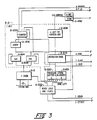
- Figure 1 shows a block diagram of a cycle production pipeline data processing system 1. Included are a central processing unit (CPU) 2, a virtual memory management unit (VMMU) 4, a cache unit 6, a memory subsystem 8, and input/output peripheral unit 10.
- the cache unit 6, memory subsystem 8, and input/output peripheral unit 10 are all coupled in common to a system bus 12.
- the memory 8 stores instructions and operands. Those operands and instructions, having the highest probability of being executed immediately, are transferred to cache unit 6 from the memory subsystem 8.
- the CPU 2 receives instructions from the cache unit 6 and in the execution of these instructions sends the virtual address portion of the instruction to VMMU 4.
- the VMMU 4 translates the virtual address into a physical address which is applied to cache unit 6 for fetching the necessary operands to allow the CPU 2 to execute the instructions.
- the input/output unit 10 represents typically any number of peripheral controllers with their devices, or an input/output processor which controls peripheral controllers and devices, or it may represent typically a communications subsystem.
- FIG. 2 shows in block diagram form the major elements that make up the CPU 2 and the cache unit 6.
- the CPU 2 includes an instruction (I) unit 2-2, an A unit 2-4, and a number of execution (E) units 2-6.
- the execution units 2-6 could be a scientific instruction processor or a commercial instruction processor. However, for simplicity of description, only the operation of one of the execution units 2-6 is described which is sufficient to understand the invention.
- the cache unit 6 includes an I-cache 6-2 and an E-cache 6-4.
- the I-cache 6-2 stores the instructions that are to be executed and the E-cache 6-4 stores the operands upon which the instructions operate.
- the I-unit 2-2 performs essentially two functions. It prefetches instructions from I-cache 6-2 and then cracks those instructions to determine how the other units, namely the A unit 2-4 and the E unit 2-6, will further process the instruction.
- the A unit 2-4 receives the instruction from the I-unit 2-2 and executes the instruction if it is a register-to-register instruction or a branch instruction.
- the A unit 2-4 sends a virtual address to the VMMU 4 which translates it into a physical address for the E-cache unit 6-4.
- E-cache 6-4 sends the operands to the E unit 2-6 for the completion of the execution of the instruction originally received by the instruction unit 2-2 from the I-cache unit 6-2.
- the A unit 2-4 will also complete the execution of branch instruction and send the branch address back to the instruction unit 2-2 so that it may request the next instruction at the location in I-cache 6-2 specified by the branch address.
- Both the A unit 2-4 and the E unit 2-6 include register files which store the contents of the registers which are accessible to the programmers, that is, so called software visible registers.
- Both the I-cache 6-2 and the E-cache 6-4 are coupled to system bus 12 and their contents are updated with instructions and operands received from memory 8.
- Instructions are executed in a production pipeline fashion by the elements of CPU 2. That is, the I unit 2-2 receives an instruction from I-cache 6-2, cracks it, and then sends the instruction to the A unit 2-4. The A unit 2-4 either executes the instruction or sends the virtual address to the VMMU 4 for translation in order to address the E-cache 6-4. E-cache 6-4 sends the designated operands to the E unit 2-6.
- the I unit 2-2 While the A unit 2-4 is executing its portion of the first instruction from the I unit 2-2, the I unit 2-2 is fetching the second instruction and subsequent instructions from I-cache 6-2.
- the I unit 2-2 sends the second instruction to the A unit 2-4.
- the VMMU 4 addresses the E-cache 6-4 while the A unit 2-4 is processing the second instruction in the pipeline.
- the VMMU 4 may be addressing E-cache 6-4 to fetch the operands of the second instruction while the A unit 2-4 is generating a virtual address of the third instruction.
- the I unit 2-2 is cracking the fourth instruction and fetching one of the subsequent instructions. Therefore, in this typical example, there could be five instructions progressing down the production line.
- the A unit 2-4 can execute certain software visible register instructions, they are removed from the production line as soon as the execution of those instructions is completed by the A unit. Similarly, when the A unit 2-4 is processing a branch instruction and the conditions of the branch are met, the A unit 2-4 immediately sends the branch address to the I unit 2-2 and that branch instruction will be removed from the production line. This mode and method of operation results in increased throughput as compared to the prior art.
- FIG. 3 shows in greater detail the elements of the instruction unit 2-2, the A unit 2-4, the execution unit 2-6 and their respective interconnections.
- the P-counter 2-200 of the instruction unit 2-2 is loaded by the A unit 2-4 with a virtual address.
- This virtual address is the address in I-cache 6-2 of the location of the next instruction that is to be placed into the pipeline.
- the virtual address is transferred to I-cache 6-2 via an adder 2-202 and either a register VA0 2-204 or a register VA1 2-206.
- Either register VA0 2-204 or register VA1 2-206 is used until a branch instruction is fetched. Then, if register VA0 2-204 is active, the address called for by the branch instruction would be stored in register VA1 2-206.
- the reason the branch address is held separately in the VA0 2-204 and VA1 2-206 registers is because if it is a conditional branch, the condition may or may not be met. If the condition is not met, then no branch will result. This gives the system the choice of either using or not using the address called for by the branch.
- the P counter 2-200 under firmware control, is incremented by one for a one word instruction, incremented by two for a double word instruction, or replaced by a branch address.
- the instruction is read out of I-cache 6-2 into either string buffers A 2-220 or string buffers B 2-221.
- one set of string buffers receives successive instructions from I-cache 6-2 until there is a branch instruction.
- the instruction following the branch instruction is stored in buffers in the other string. For example, if the string buffers A 2-220 were being used then the instruction following the branch instructions would be stored in the string buffers B 2-221.
- the throughput is improved by storing both sets of instructions in case the branch conditions are met and the I unit 2-4 fetches the branch string from string buffers B 2-221.
- the instruction is then sent to the instruction crack and resource control unit 2-210 which determines the kind of instruction it is. That is, if this is a software visible register to register instruction, then it will be executed by the A unit 2-4 if it is a memory instruction that will be executed by the E unit 2-6.
- the instruction is sent from the crack unit 2-210 to an A-unit firmware address generator 2-208 which addresses an A-unit control store 2-430.
- the contents of the addressed location is stored in an RDR (A) register 2-406 in the A unit 2-4.
- the instruction signals I INSTR 0-31 from the string buffers 2-220 or 2-221 are transferred to the instruction (RINSTR) register 2-400 in the A-unit 2-4.
- the instruction is to be executed by the E unit 2-6 it is also stored in an instruction first in a first out register (FIFO) 2-600 in the E unit 2-6.
- the instruction is also stored in an OP-CODE register 2-402 in the A unit 2-4 under control of a signal I-BEGIN from the I unit 2-4.
- Both the RINSTR register 2-400 and the OP CODE register 2-402 store double words of 32 bits each. If an instruction requires 2 or 3 double words, then the OP CODE for that instruction remains in the OP CODE register 2-402 while each of the double words of the instruction in turn are stored in the instruction register 2-400.
- the output of the OP CODE register 2-402 is used primarily for addressing a register file 2-404 under control of OP CODE and firmware bits stored in the OP CODE register 2-402 and the register RDR (A) 2-406 respectively.
- the register file 2-404 includes the software visible registers. If the instruction being executed is a memory instruction, then a virtual address is generated and sent to the VMMU 4 via an arithmetic logic unit (ALU) 2-412. Depending upon the instruction being executed by the A unit 2-6, the input to the ALU 2-412 may be applied to the A side, by the RINSTR register 2-400, the OP CODE register 2-402, the register file 2-404 or a program counter 2-416.
- ALU arithmetic logic unit
- ALU 2-412 B side inputs are provided by an index shifter 2-410 for index or offset operations, via an adder 2-408 or from register file 2-404. If this is a register instruction, for example, a shift operation of the contents of a software visible register in the register file 2-404, then the output of the register file 2-404 may be applied to the shifter 2-414, be shifted the number of bits specified by the instruction and stored back in the register file 2-404 in the same register from which it was read.
- signals from RINSTR 2-400 and from the ALU 2-412 are applied to branch logic 2-401.
- the output, load signal A-P-LD enables the P counter 2-200 to accept the branch address signals A-BRANCH which are sent to I-CACHE 6-2.
- an A-DONE signal is sent to the crack unit 2-210 of the I unit 2-2. This informs the I unit 2-2 to send the next instruction stored in the string buffers 2-220 or 2-221 to the A unit 2-4 and if required, to the E unit 2-6. If an instruction calls for execution by the E unit 2-6, then the I unit 2-2 sends that instruction to the instruction FIFO 2-600 under control of signal I-E-LAST and signal I-E-FIRST. These signals control the loading of the instruction FIFO 2-600.
- the boolean expressions describing the signals appear in the appendix and should be referenced to where appropriate.
- the I-BEGIN signal is received by the A unit 2-4 when the CRACK signal is generated, the system is not in a hold mode and no logic block including the clock logic is in a stall mode.
- the CRACK signal is generated when the ready logic and flops 2-222 is ready to crack the instruction, the string buffers A 2-220 or string buffers B 2-221 store at least one instruction, and the A unit 2-4 had generated the ADONE signal indicating that the A unit is available for processing the next instruction.
- the I unit 2-2 generates the I-EFIRST and the I-ELAST signals by the ready logic and flops 2-222 if the instruction being cracked is to be executed by the E unit 2-6. Both signals are applied to the I FIFO 2-600.
- the I-EFIRST signal enables the I-FIFO 2-600 to store a double word instruction.
- the I-ELAST signal enables the I-FIFO 2-600 to store a single word instruction.
- the I unit 2-2 sends the instruction to be executed in the A unit 2-4, and only to FIFO 2-600 if the instruction is to be executed in the E unit 2-6.
- the next instruction the FIFO 2-600 will execute is applied to the next address generator 2-602 which generates the E unit control store 2-604 address location.
- the firmware word is stored in a register RDR (E) 2-606.
- the instruction FIFO 2-600 stores up to four instructions.
- the VMMU 4 When the A unit 2-4 sends its virtual address to the VMMU 4, the VMMU 4 generates the physical address which addresses the E-cache 6-4.
- the contents of the addressed location is stored in a data FIFO 2-630 in the E unit 2-6 by signal LD-DAT-0015 for a single word transfer or signal LD-DAT 1631 for a double word transfer.
- Signal LD-DAT-0015 also increments by one the FIFO 2-630 write address to accept the second word of the transfer if the first word was not at an E-CACHE 6-4 word boundary.
- This data is the operands on which the instruction will operate.
- the E-unit 2-6 executes instructions whose operands are stored in software visible registers of register file 2-630.
- a typical instruction is the multiply instruction.
- the A unit 2-4 For this instruction, the A unit 2-4 generates a dummy cycle by sending the virtual address hexadecimal 40 to the VMMU 4. This results in the E-CACHE 6-4 generating a dummy cycle by sending signal LD-DAT 1631 to the FIFO 2-630 with a "dummy" operand.
- the displacement from the crack unit 2-210 is applied to the adder 2-202 to be added to the contents of the P counter 2-200 and stored in either register VA0 2-204 or register VA1 2-206 and applied to the I-cache 6-2.
- a multiplier 2-616 is coupled to the A & B ports of register file 2-610 to generate and store partial products in conjunction with the shifter 2-618 and the Q-register 2-620.
- the partial products are applied to a result multiplexer (MUX) 2-622 and stored in accumulator location in register file 2-610.
- MUX result multiplexer
- a swapper logic 2-612 receives operands from the B side of register file 2-610 for swapping words within double words and swapping bytes within single words.
- a 16-bit word is made up of two 8-bit bytes.
- a double word is made up of two 16-bit single words or four 8-bit bytes.
- a sign extender 2-614 repeats the sign of all the high order positions of a double word to the left of the first significant bit of the double word.
- the CT1 and CT2 counters 2-624 are used in the calculation of the exponent of a floating point resultant.
- a mantissa of a floating point operand is processed through the ALU 2-608 and a shifter 2-618 in a conventional manner.
- the software visible registers in both the register files 2-404 with A unit 2-4 and 2-610 in the E unit 2-6 are updated on successive cycles so that they both contain the same information. This is accomplished by firmware signals from register RDR (A) 2-406 which are applied to logic 2-420 to generate an update signal A-UPDT which enables the register file 2-610 and six A-ADR signals which are applied to the address terminals of register file 2-610 to store the data from the D terminal of the register file 2-404 to the D terminal of register file 2-610.
- the E-UPDT signal from register RDR (E) 2-606 enable register file 2-404 to store the data at the address specified by signals E-ADR from logic 2-601.
- Logic 2-601 signals E-ADR as a result of instruction signals from the instruction FIFO 2-600 and firmware signals from RDR (E) 2-606.
- the A unit 2-4 program counter 2-416 stores the address of the next instruction.
- P counter 2-200 in the I unit 2-2 also stores the address of the next instruction.
- the reason for the two registers is that, in case of a conditional branch, P counter 2-200 in the I unit 2-2 stores the branch address in case it is to be used, whereas the program counter 2-416 will not store the branch address but stores the next address in the sequence presently being executed.
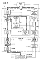
- a virtual address is applied to the virtual address register 4-101 from address unit and commands signals are entered in the VMMU command register 4-106, both from address registers.
- the contents of the virtual address register 4-101 is applied to the arithmetic logic unit 4-103, to the VMMU associative memory unit 4-102, to the VMMU security monitor unit 4-105 and to the VMMU control logic unit 4-107.
- the output signals from the arithmetic logic unit 4-103 are applied to the plus one register 4-104.
- the output signals from the plus one register 4-104 are applied to the VMMU associative memory unit 4-102 and to the security monitor unit 4-105.
- Output signals from the security monitor unit 4-105 are applied to the VMMU control logic unit 4-107.
- Output signals from the VMMU associative memory unit 4-102 are applied to the VMMU output register 4-108, while the output signals from the VMMU control logic unit 4-107 are applied to the VMMU command output register 4-109.
- the output signals from the E-cache output register 6-405 of the E-cache unit 6-4 are applied to register 2-601 of the execution unit 2-6.
- the output signals of the E-cache control logic unit 6-404 are applied to the execution unit and control the flow of operands between the E-cache unit and the execution unit.
- the operation of the present invention can be understood by reference to Fig. 5 as interpreted in view of Fig. 6.
- the V-RDY signal controls the transfer of the virtual addresses from the address unit 2-4 to the virtual address register 4-101. During the periods (i.e., machine cycles) 1-3, the current virtual address is stored in the virtual address register 4-101. During period 4, the processing of the virtual address will be complete and the V-RDY signal is applied to the address unit 2-4 to insure that the next virtual address will be stored in the virtual address register during the next period.
- the V-RDY signal also causes command signals to be read into the VMMU command register so that these signals will be available during period 1 and during period 5.
- the command signals in the VMMU command input register 4-106 indicate that an operand is to be read from the E-cache unit.
- the state of bit position 31 in the virtual address register 4-101 is applied to the VMMU control logic unit 4-107.
- the read command signals in conjunction with a logic "1" in bit position 31 results in the procedure for reading an operand that crosses the double word boundary.
- the contents of the virtual address register are applied to arithmetic logic unit 4-103 wherein a "1" is addressed to the least significant bit position from the virtual address register 4-101 in response to the PLUS ONE signal.
- the result from the arithmetic logic unit 4-103 is stored in the plus one register 4-104.
- the contents of the plus one register 4-104 are forwarded in the presence of the SCND signal while the contents of the virtual address register 4-101 are forwarded in the presence of the SCND NOT signal.
- the SCND NOT signal of period 1 indicates that the contents of virtual address register 4-101 are applied to the input terminals of the VMMU associative memory unit 4-102 and to the security monitor unit 4-105.
- the TRANSLATE signal causes the security monitor unit 4-105 to determine the attributes associated with the segment number, e.g., via a look-up table, and to compare the segment number attributes with the ring number of the virtual address. The result of this comparison is applied to the VMMU control logic unit 4-107. When the comparison is negative, the program is not permitted access to the segment and a special routine must be entered to determine how to respond to the lack of access. When the comparison is positive the signals of the period 2 are imposed by the VMMU control logic unit 4-107.
- the SCND signal causes the contents of the plus one register 4-104 to be applied to the VMMU associative memory unit 4-102 and to the security monitor unit 4-105.
- the TRANSLATE signal causes the security monitor unit 4-105 to compare the attributes associated with the segment number with the ring number. When this comparison is positive, then the two double word operands having the required two words can be accessed by the program and the procedure is allowed to continue. As part of the security checking procedure, a determination can be made whether the page (or pages) including the two words of the required double word are currently stored in the memory unit 8.
- the SCND NOT signal permits the contents of the virtual address register to be applied to the VMMU associative memory unit 4-102.
- the presence of the ECTL signal causes the associated real address to be retrieved from the VMMU associative memory unit 4-102 and applied to VMMU output register 4-108.
- the presence of the V-VAL signal causes the E-cache read address register 6-401 to have the contents of the VMMU output register 4-108 applied thereto.
- the V-VAL signals have permitted signals for the VMMU control logic unit 4-107 to be applied to the E-cache control logic unit 6-404 via the VMMU command output register 4-109 and the E-cache command register 6-403.
- the E-cache control logic unit 6-404 applies the READ RAM signal and, during period 3, applies the LOAD OUTPUT signal to the E-cache output register 6-405, and applies the LD-DATA 16-31 to the execution unit 2-6.
- the LD-DATA 16-31 causes the second word of the double word operand stored in E-cache output register 6-405 to become the first word of the resulting operand stored in register 2-601.
- the V-RDY signal causes the next virtual address to be entered in the virtual address register 4-101.
- the contents of the E-cache real address register 6-401 are applied to the E-cache associative memory unit 6-402 as a result of the READ RAM signal and the LOAD OUTPUT signal from the E-cache control logic unit 6-404.
- the LD-DATA 0-15 signal for the E-cache control logic unit to the execution unit 2-6 causes the first 16 bits of the double word stored in the E-cache output register 6-405 to become the second 16 bit word in the double word stored in register 2-601 of the execution unit 2-6.
Landscapes
- Engineering & Computer Science (AREA)
- Theoretical Computer Science (AREA)
- Physics & Mathematics (AREA)
- General Engineering & Computer Science (AREA)
- General Physics & Mathematics (AREA)
- Memory System Of A Hierarchy Structure (AREA)
- Executing Machine-Instructions (AREA)
- Advance Control (AREA)
Abstract
Description
- This invention relates generally to data processing systems and, more particularly, to data processing systems in which a data processing unit identifies a data group by a first (virtual) address while the same data group is identified in the memory unit by a second (real) address.
- In the multiprocessor, multiprogramming data processing systems, the allocation of memory locations for each program, formerly under the control of the programmer, has now become the province of the operating system. The program identifies data groups by virtual addresses, the virtual addresses only indirectly related to a physical location in the memory space of the data processing system. The use of the virtual addressing technique permits the data processing unit to have access to a large data storage facility even though only a small fraction of the available data groups will be resident in the memory unit at any one time. On the other hand, the real address of a data group relates to a physical memory location. The operating system has the responsibility for establishing the correspondence of the virtual addresses used by the executing program and the real addresses having significance for the data processing system. In the data processing system, a translation unit, typically referred to as the virtual memory management unit, provides an address in the memory unit in response to a virtual address used by the executing program. The virtual memory management unit includes apparatus for insuring that a data processing system program does not access inappropriate data groups.
- In the modern data processing system, the data groups are typically organized into consecutive blocks. Because data groups which are potentially capable of being processed in close temporal proximity are stored in neighboring memory locations, a high probability exists that a data group of a neighboring memory location will be required relatively soon after the originally required data group is processed. The transfer of blocks of consecutive data groups to a data processing system for each memory read operation can reduce the number of memory accesses required to execute a program sequence. In the preferred embodiment, a block of data includes two double words, or 32 bits. Each word is addressed by a 32 bit address of the form illustrated in Fig. 4. The
bits Bits 2 through 11 identify the segment number, the coursest granularity for the identification of storage addresses.Bits 12 through 21 relate to a page number, the page being the unit of storage in the memory unit.Bits 22 through 31 identify the address offset, the offset address defining the relative location of the data group within the page. - The execution unit is implemented to process properly aligned double word operands. When the double word boundary is strictly enforced in a data processing system, then
bit 31 of the virtual address would be redundant. As a practical matter, a double word can begin with the second word of the double word, or whenbit 31 is a logic "1" signal. Whenbit 31 is a logic "1", then the second word is across the normal double word boundary and is the first word of the next double word. As a practical matter, this boundary crossing can cause problems with respect to the access of the second word. First, the addition of a logic "1" to the logic "1" ofbit 31 can result in a memory address that is currently stored in the memory unit. Second, when the address offset consists of all logic "1"s inbit positions 22 through 31, the addition of a logic "1" to determine the second word of the double word will fall in a next page, a page that may not be present in the main memory. In this situation, the operating system be invoked to move the missing page into main memory. Finally, if the page number and the address offset, i.e.,bits 12 through 31 are all logic "1"s, then the addition of a logic "1" to the 31 bit position results in a new segment being identified. Each segment can have different privileges associated therewith so that the second word of the double word may not be accessible to the currently executing instruction. - Therefore, a need has been felt for a virtual memory management unit in a data processing system that can provide the two words of a double word that cross a double word boundary or, in the alternative indicate why the double word can not be provided.
- It is an object of the present invention to provide an improved data processing system.
- It is a feature of the present invention to provide an improved data processing unit in which virtual addresses are used to identify data groups.
- It is another feature of the present invention to provide apparatus for aligning a double word operand that is stored across a double word boundary.
- It is yet another feature of the present invention to compare attributes of two double word operands, each operand containing a word of a required operand stored across a double word boundary.
- The aforementioned and other features are accomplished, according to the present invention, by providing apparatus for identifying when an operand to be read from the E-cache memory unit crosses a double word boundary. When the boundary crossing operand is identified, the VMMU unit compares the attributes associated with the virtual addresses of each word of the required double word with the ring number associated with the virtual address. When the comparison indicates that the required double word operand is available to the program, then each virtual address is translated in a real address of a double word which includes one word of the required double word. The two words of the required double word are stored in a register in the correct order and the required double word is available to the execution unit for processing.
- These and other features of the invention will be understood upon reading of the following description along with the drawings.
-
- Figure 1 is a block diagram of the overall system which includes the apparatus of the present invention.
- Figure 2 is a more detailed block diagram of the overall system of Figure 1.
- Figure 3 is a logic block diagram of major elements of the production pipeline cycles.
- Figure 4 illustrates the portions of a virtual address according to the preferred embodiment.
- Figure 5 is a block diagram of the components for performing the virtual address translation according to the present invention.
- Figure 6 shows the process of performing the virtual to real address translation as a function of consecutive machine cycles according to the present invention.
- The present invention is adapted to function in a data processing unit in which certain types of instructions are executed by an earlier unit and dropped out of the production line while other types of instructions are executed at the end of the production line. The address unit of the data processing unit invention includes means for executing the instruction if it is a "non memory" instruction. The "non-memory" instruction by having been executed during the third cycle of operation is effectively dropped or removed from the production line and therefore requires no further cycles in the production line thereby improving the system throughput.
- Figure 1 shows a block diagram of a cycle production pipeline
data processing system 1. Included are a central processing unit (CPU) 2, a virtual memory management unit (VMMU) 4, acache unit 6, amemory subsystem 8, and input/outputperipheral unit 10. Thecache unit 6,memory subsystem 8, and input/outputperipheral unit 10 are all coupled in common to asystem bus 12. Thememory 8 stores instructions and operands. Those operands and instructions, having the highest probability of being executed immediately, are transferred tocache unit 6 from thememory subsystem 8. - The
CPU 2 receives instructions from thecache unit 6 and in the execution of these instructions sends the virtual address portion of the instruction to VMMU 4. The VMMU 4 translates the virtual address into a physical address which is applied tocache unit 6 for fetching the necessary operands to allow theCPU 2 to execute the instructions. - The input/
output unit 10 represents typically any number of peripheral controllers with their devices, or an input/output processor which controls peripheral controllers and devices, or it may represent typically a communications subsystem. - Figure 2 shows in block diagram form the major elements that make up the
CPU 2 and thecache unit 6. TheCPU 2 includes an instruction (I) unit 2-2, an A unit 2-4, and a number of execution (E) units 2-6. The execution units 2-6 could be a scientific instruction processor or a commercial instruction processor. However, for simplicity of description, only the operation of one of the execution units 2-6 is described which is sufficient to understand the invention. - The
cache unit 6 includes an I-cache 6-2 and an E-cache 6-4. The I-cache 6-2 stores the instructions that are to be executed and the E-cache 6-4 stores the operands upon which the instructions operate. The I-unit 2-2 performs essentially two functions. It prefetches instructions from I-cache 6-2 and then cracks those instructions to determine how the other units, namely the A unit 2-4 and the E unit 2-6, will further process the instruction. - The A unit 2-4 receives the instruction from the I-unit 2-2 and executes the instruction if it is a register-to-register instruction or a branch instruction. When the instruction is to be executed by the E unit 2-6, the A unit 2-4 sends a virtual address to the VMMU 4 which translates it into a physical address for the E-cache unit 6-4. E-cache 6-4 sends the operands to the E unit 2-6 for the completion of the execution of the instruction originally received by the instruction unit 2-2 from the I-cache unit 6-2.
- The A unit 2-4 will also complete the execution of branch instruction and send the branch address back to the instruction unit 2-2 so that it may request the next instruction at the location in I-cache 6-2 specified by the branch address. Both the A unit 2-4 and the E unit 2-6 include register files which store the contents of the registers which are accessible to the programmers, that is, so called software visible registers. Both the I-cache 6-2 and the E-cache 6-4 are coupled to
system bus 12 and their contents are updated with instructions and operands received frommemory 8. - Instructions are executed in a production pipeline fashion by the elements of
CPU 2. That is, the I unit 2-2 receives an instruction from I-cache 6-2, cracks it, and then sends the instruction to the A unit 2-4. The A unit 2-4 either executes the instruction or sends the virtual address to the VMMU 4 for translation in order to address the E-cache 6-4. E-cache 6-4 sends the designated operands to the E unit 2-6. - While the A unit 2-4 is executing its portion of the first instruction from the I unit 2-2, the I unit 2-2 is fetching the second instruction and subsequent instructions from I-cache 6-2. When the A unit 2-4 sends the virtual address specified by the first instruction to the VMMU 4 and notifies the I unit 2-2 of that event, the I unit 2-2 sends the second instruction to the A unit 2-4. The VMMU 4 addresses the E-cache 6-4 while the A unit 2-4 is processing the second instruction in the pipeline. When the E unit 2-6 is executing the first instruction, the VMMU 4 may be addressing E-cache 6-4 to fetch the operands of the second instruction while the A unit 2-4 is generating a virtual address of the third instruction. Meanwhile, the I unit 2-2 is cracking the fourth instruction and fetching one of the subsequent instructions. Therefore, in this typical example, there could be five instructions progressing down the production line.
- However, since the A unit 2-4 can execute certain software visible register instructions, they are removed from the production line as soon as the execution of those instructions is completed by the A unit. Similarly, when the A unit 2-4 is processing a branch instruction and the conditions of the branch are met, the A unit 2-4 immediately sends the branch address to the I unit 2-2 and that branch instruction will be removed from the production line. This mode and method of operation results in increased throughput as compared to the prior art.
- Figure 3 shows in greater detail the elements of the instruction unit 2-2, the A unit 2-4, the execution unit 2-6 and their respective interconnections. The P-counter 2-200 of the instruction unit 2-2 is loaded by the A unit 2-4 with a virtual address. This virtual address is the address in I-cache 6-2 of the location of the next instruction that is to be placed into the pipeline. During the I-FETCH cycle, the virtual address is transferred to I-cache 6-2 via an adder 2-202 and either a register VA0 2-204 or a register VA1 2-206. Either register VA0 2-204 or register VA1 2-206 is used until a branch instruction is fetched. Then, if register VA0 2-204 is active, the address called for by the branch instruction would be stored in register VA1 2-206.
- The reason the branch address is held separately in the VA0 2-204 and VA1 2-206 registers is because if it is a conditional branch, the condition may or may not be met. If the condition is not met, then no branch will result. This gives the system the choice of either using or not using the address called for by the branch. The P counter 2-200, under firmware control, is incremented by one for a one word instruction, incremented by two for a double word instruction, or replaced by a branch address.
- The instruction is read out of I-cache 6-2 into either string buffers A 2-220 or string buffers B 2-221. Here again, one set of string buffers receives successive instructions from I-cache 6-2 until there is a branch instruction. Then the instruction following the branch instruction is stored in buffers in the other string. For example, if the string buffers A 2-220 were being used then the instruction following the branch instructions would be stored in the string buffers B 2-221. The throughput is improved by storing both sets of instructions in case the branch conditions are met and the I unit 2-4 fetches the branch string from string buffers B 2-221.
- The instruction is read out of I-cache 6-2 into either string buffers A 2-220 or string buffers B 2-221. Here again, one set of string buffers receives successive instructions from I-cache 6-2 until there is a branch instruction. Then the instruction following the branch instruction is stored in buffers in the other string. For example, if the string buffers A 2-220 were being used then the instruction following the branch instructions would be stored in the string buffers B 2-221. The throughput is improved by storing both sets of instructions in case the branch conditions are met and the I unit 2-4 fetches the branch string from string buffers B 2-221.
- The instruction is then sent to the instruction crack and resource control unit 2-210 which determines the kind of instruction it is. That is, if this is a software visible register to register instruction, then it will be executed by the A unit 2-4 if it is a memory instruction that will be executed by the E unit 2-6.
- The instruction is sent from the crack unit 2-210 to an A-unit firmware address generator 2-208 which addresses an A-unit control store 2-430. The contents of the addressed location is stored in an RDR (A) register 2-406 in the A unit 2-4. The instruction signals I INSTR 0-31 from the string buffers 2-220 or 2-221 are transferred to the instruction (RINSTR) register 2-400 in the A-unit 2-4. If the instruction is to be executed by the E unit 2-6 it is also stored in an instruction first in a first out register (FIFO) 2-600 in the E unit 2-6. The instruction is also stored in an OP-CODE register 2-402 in the A unit 2-4 under control of a signal I-BEGIN from the I unit 2-4. Both the RINSTR register 2-400 and the OP CODE register 2-402 store double words of 32 bits each. If an instruction requires 2 or 3 double words, then the OP CODE for that instruction remains in the OP CODE register 2-402 while each of the double words of the instruction in turn are stored in the instruction register 2-400.
- The output of the OP CODE register 2-402 is used primarily for addressing a register file 2-404 under control of OP CODE and firmware bits stored in the OP CODE register 2-402 and the register RDR (A) 2-406 respectively. The register file 2-404 includes the software visible registers. If the instruction being executed is a memory instruction, then a virtual address is generated and sent to the VMMU 4 via an arithmetic logic unit (ALU) 2-412. Depending upon the instruction being executed by the A unit 2-6, the input to the ALU 2-412 may be applied to the A side, by the RINSTR register 2-400, the OP CODE register 2-402, the register file 2-404 or a program counter 2-416. ALU 2-412 B side inputs are provided by an index shifter 2-410 for index or offset operations, via an adder 2-408 or from register file 2-404. If this is a register instruction, for example, a shift operation of the contents of a software visible register in the register file 2-404, then the output of the register file 2-404 may be applied to the shifter 2-414, be shifted the number of bits specified by the instruction and stored back in the register file 2-404 in the same register from which it was read.
- For the conditional branch instruction, signals from RINSTR 2-400 and from the ALU 2-412 are applied to branch logic 2-401. The output, load signal A-P-LD, enables the P counter 2-200 to accept the branch address signals A-BRANCH which are sent to I-CACHE 6-2.
- When the A unit 2-4 has completed the execution of the instruction, an A-DONE signal is sent to the crack unit 2-210 of the I unit 2-2. This informs the I unit 2-2 to send the next instruction stored in the string buffers 2-220 or 2-221 to the A unit 2-4 and if required, to the E unit 2-6. If an instruction calls for execution by the E unit 2-6, then the I unit 2-2 sends that instruction to the instruction FIFO 2-600 under control of signal I-E-LAST and signal I-E-FIRST. These signals control the loading of the instruction FIFO 2-600.
- The boolean expressions describing the signals appear in the appendix and should be referenced to where appropriate. The I-BEGIN signal is received by the A unit 2-4 when the CRACK signal is generated, the system is not in a hold mode and no logic block including the clock logic is in a stall mode.
- The CRACK signal is generated when the ready logic and flops 2-222 is ready to crack the instruction, the string buffers A 2-220 or string buffers B 2-221 store at least one instruction, and the A unit 2-4 had generated the ADONE signal indicating that the A unit is available for processing the next instruction.
- The I unit 2-2 generates the I-EFIRST and the I-ELAST signals by the ready logic and flops 2-222 if the instruction being cracked is to be executed by the E unit 2-6. Both signals are applied to the I FIFO 2-600. The I-EFIRST signal enables the I-FIFO 2-600 to store a double word instruction. The I-ELAST signal enables the I-FIFO 2-600 to store a single word instruction.
- Note that the I unit 2-2 sends the instruction to be executed in the A unit 2-4, and only to FIFO 2-600 if the instruction is to be executed in the E unit 2-6. In the E unit 2-6, the next instruction the FIFO 2-600 will execute is applied to the next address generator 2-602 which generates the E unit control store 2-604 address location. The firmware word is stored in a register RDR (E) 2-606. The instruction FIFO 2-600 stores up to four instructions.
- When the A unit 2-4 sends its virtual address to the VMMU 4, the VMMU 4 generates the physical address which addresses the E-cache 6-4. The contents of the addressed location is stored in a data FIFO 2-630 in the E unit 2-6 by signal LD-DAT-0015 for a single word transfer or signal LD-DAT 1631 for a double word transfer. Signal LD-DAT-0015 also increments by one the FIFO 2-630 write address to accept the second word of the transfer if the first word was not at an E-CACHE 6-4 word boundary. This data is the operands on which the instruction will operate. The E-unit 2-6 executes instructions whose operands are stored in software visible registers of register file 2-630. A typical instruction is the multiply instruction.
- For this instruction, the A unit 2-4 generates a dummy cycle by sending the virtual address hexadecimal 40 to the VMMU 4. This results in the E-CACHE 6-4 generating a dummy cycle by sending signal LD-DAT 1631 to the FIFO 2-630 with a "dummy" operand.
- If in the I unit 2-2, the instruction calls for a branch and has a displacement, then the displacement from the crack unit 2-210 is applied to the adder 2-202 to be added to the contents of the P counter 2-200 and stored in either register VA0 2-204 or register VA1 2-206 and applied to the I-cache 6-2.
- A multiplier 2-616 is coupled to the A & B ports of register file 2-610 to generate and store partial products in conjunction with the shifter 2-618 and the Q-register 2-620. The partial products are applied to a result multiplexer (MUX) 2-622 and stored in accumulator location in register file 2-610. When the multiplication is completed the final result is stored in one of the software visible registers of register file 2-610.
- A swapper logic 2-612 receives operands from the B side of register file 2-610 for swapping words within double words and swapping bytes within single words. A 16-bit word is made up of two 8-bit bytes. A double word is made up of two 16-bit single words or four 8-bit bytes. A sign extender 2-614 repeats the sign of all the high order positions of a double word to the left of the first significant bit of the double word.
- The CT1 and CT2 counters 2-624 are used in the calculation of the exponent of a floating point resultant. A mantissa of a floating point operand is processed through the ALU 2-608 and a shifter 2-618 in a conventional manner.
- The software visible registers in both the register files 2-404 with A unit 2-4 and 2-610 in the E unit 2-6 are updated on successive cycles so that they both contain the same information. This is accomplished by firmware signals from register RDR (A) 2-406 which are applied to logic 2-420 to generate an update signal A-UPDT which enables the register file 2-610 and six A-ADR signals which are applied to the address terminals of register file 2-610 to store the data from the D terminal of the register file 2-404 to the D terminal of register file 2-610. Similarly, the E-UPDT signal from register RDR (E) 2-606 enable register file 2-404 to store the data at the address specified by signals E-ADR from logic 2-601. Logic 2-601 signals E-ADR as a result of instruction signals from the instruction FIFO 2-600 and firmware signals from RDR (E) 2-606.
- The A unit 2-4 program counter 2-416 stores the address of the next instruction. P counter 2-200 in the I unit 2-2 also stores the address of the next instruction. The reason for the two registers is that, in case of a conditional branch, P counter 2-200 in the I unit 2-2 stores the branch address in case it is to be used, whereas the program counter 2-416 will not store the branch address but stores the next address in the sequence presently being executed.
- Referring next to Fig. 4, the composition of the virtual address according to the preferred embodiment has been described above.
- Referring now to Fig. 5, a block diagram of the data processing unit components in the virtual address translation process according to the present invention is shown. In response to a V-RDY signal from VMMU control logic unit 4-107, a virtual address is applied to the virtual address register 4-101 from address unit and commands signals are entered in the VMMU command register 4-106, both from address registers. The contents of the virtual address register 4-101 is applied to the arithmetic logic unit 4-103, to the VMMU associative memory unit 4-102, to the VMMU security monitor unit 4-105 and to the VMMU control logic unit 4-107. The output signals from the arithmetic logic unit 4-103 are applied to the plus one register 4-104. The output signals from the plus one register 4-104 are applied to the VMMU associative memory unit 4-102 and to the security monitor unit 4-105. Output signals from the security monitor unit 4-105 are applied to the VMMU control logic unit 4-107. Output signals from the VMMU associative memory unit 4-102 are applied to the VMMU output register 4-108, while the output signals from the VMMU control logic unit 4-107 are applied to the VMMU command output register 4-109.
- The output signals from the VMMU output register 4-108 of the VMMU unit 4 are applied to the data FIFO address register 2-630 of the E-cache unit 6-4. The command signals from the VMMU command output register 4-109 are applied to the E-cache command register 6-403 of the E-cache unit 6-4. The output signals from the E-cache read address register 6-401 are applied to the E-cache associative memory unit 6-402. The output signals from the E-cache associative memory unit 6-402 are applied to the E-cache output register 6-405. The output signals from the E-cache command register 6-403 are applied to the E-cache control logic unit 6-404.
- The output signals from the E-cache output register 6-405 of the E-cache unit 6-4 are applied to register 2-601 of the execution unit 2-6. The output signals of the E-cache control logic unit 6-404 are applied to the execution unit and control the flow of operands between the E-cache unit and the execution unit.
- The operation of the present invention can be understood by reference to Fig. 5 as interpreted in view of Fig. 6. The V-RDY signal controls the transfer of the virtual addresses from the address unit 2-4 to the virtual address register 4-101. During the periods (i.e., machine cycles) 1-3, the current virtual address is stored in the virtual address register 4-101. During period 4, the processing of the virtual address will be complete and the V-RDY signal is applied to the address unit 2-4 to insure that the next virtual address will be stored in the virtual address register during the next period. The V-RDY signal also causes command signals to be read into the VMMU command register so that these signals will be available during
period 1 and during period 5. For the present invention, the command signals in the VMMU command input register 4-106 indicate that an operand is to be read from the E-cache unit. In addition, the state ofbit position 31 in the virtual address register 4-101 is applied to the VMMU control logic unit 4-107. The read command signals in conjunction with a logic "1" inbit position 31 results in the procedure for reading an operand that crosses the double word boundary. The contents of the virtual address register are applied to arithmetic logic unit 4-103 wherein a "1" is addressed to the least significant bit position from the virtual address register 4-101 in response to the PLUS ONE signal. The result from the arithmetic logic unit 4-103 is stored in the plus one register 4-104. The contents of the plus one register 4-104 are forwarded in the presence of the SCND signal while the contents of the virtual address register 4-101 are forwarded in the presence of the SCND NOT signal. The SCND NOT signal ofperiod 1 indicates that the contents of virtual address register 4-101 are applied to the input terminals of the VMMU associative memory unit 4-102 and to the security monitor unit 4-105. The TRANSLATE signal causes the security monitor unit 4-105 to determine the attributes associated with the segment number, e.g., via a look-up table, and to compare the segment number attributes with the ring number of the virtual address. The result of this comparison is applied to the VMMU control logic unit 4-107. When the comparison is negative, the program is not permitted access to the segment and a special routine must be entered to determine how to respond to the lack of access. When the comparison is positive the signals of theperiod 2 are imposed by the VMMU control logic unit 4-107. - In
period 2, the SCND signal causes the contents of the plus one register 4-104 to be applied to the VMMU associative memory unit 4-102 and to the security monitor unit 4-105. The TRANSLATE signal causes the security monitor unit 4-105 to compare the attributes associated with the segment number with the ring number. When this comparison is positive, then the two double word operands having the required two words can be accessed by the program and the procedure is allowed to continue. As part of the security checking procedure, a determination can be made whether the page (or pages) including the two words of the required double word are currently stored in thememory unit 8. - In period 3, the reading of the two words of the double word having been determined not to be prohibited, the SCND NOT signal permits the contents of the virtual address register to be applied to the VMMU associative memory unit 4-102. The presence of the ECTL signal causes the associated real address to be retrieved from the VMMU associative memory unit 4-102 and applied to VMMU output register 4-108. The presence of the V-VAL signal causes the E-cache read address register 6-401 to have the contents of the VMMU output register 4-108 applied thereto.
- With respect to the access to the VMMU associative memory unit 4-102, it will be clear to those skilled in art of virtual memory management techniques that a portion of the address from the virtual address unit is not translated and can be applied directly to the VMMU output register. These data paths have not been illustrated to focus on the operation of the present invention.
- In period 4, the SCND signal causes the contents of the plus one register 4-104 to be applied to the VMMU associative memory unit 4-102 while the EO signal caused the output signals of the VMMU associative memory unit 4-102 to be applied to the VMMU output register 4-108. The V-VAL signal causes the contents of the VMMU output register to be applied to the E-cache read address register. The current contents of the E-cache read address register 6-401 is applied to the E-cache associative memory unit 6-402 and, in the presence of the READ RAM signal, the output signals from the E-cache associative memory unit 6-402 are applied to the E-cache output register 6-405. The V-VAL signals have permitted signals for the VMMU control logic unit 4-107 to be applied to the E-cache control logic unit 6-404 via the VMMU command output register 4-109 and the E-cache command register 6-403. The E-cache control logic unit 6-404 applies the READ RAM signal and, during period 3, applies the LOAD OUTPUT signal to the E-cache output register 6-405, and applies the LD-DATA 16-31 to the execution unit 2-6. The LD-DATA 16-31 causes the second word of the double word operand stored in E-cache output register 6-405 to become the first word of the resulting operand stored in register 2-601. In period 4, the V-RDY signal causes the next virtual address to be entered in the virtual address register 4-101.
- In period 5, the contents of the E-cache real address register 6-401 are applied to the E-cache associative memory unit 6-402 as a result of the READ RAM signal and the LOAD OUTPUT signal from the E-cache control logic unit 6-404. The LD-DATA 0-15 signal for the E-cache control logic unit to the execution unit 2-6 causes the first 16 bits of the double word stored in the E-cache output register 6-405 to become the second 16 bit word in the double word stored in register 2-601 of the execution unit 2-6.
- The description of the operation of the preferred embodiment requires four period (machine cycles in the pipelined data processing unit) to complete. It will be clear that with appropriate logic apparatus and control signals, the access of the VMMU associative memory can be performed concurrently with the operation of the security monitor unit and the resulting real address or resulting operand word stored pending the results of the attribute/ring number comparison. Because the crossing of a double word boundary is relatively rare in the preferred embodiment, the increased efficiency data processing unit instruction execution does not warrant the additional apparatus.
- Although the present invention is adapted to operate with a data processing unit described in relation to Figures 1-3, it will be clear to those skilled in the art that the technique of translation of a virtual address that crosses a boundary of a group of words is applicable to other data processing unit configurations.
- It will be further clear to those skilled in the art that the performance of the present invention can be increased by placing a buffer storage unit in the position of the VMMU output register 4-108 so that the access to the VMMU associative memory unit 4-102 can function simultaneously with the testing by the security monitor.
- The foregoing description is provided to illustrate the operation of the preferred embodiment and is not meant to limit the scope of the invention. The scope of the invention is to be limited only by the following claims. From the foregoing description, many variations will be apparent to those skilled in the art that would yet be encompassed by the spirit and scope of the invention.
Claims (18)
a execution unit for processing aligned double word operands;
a cache memory unit for storing double operands, wherein two cache memory locations can store a word of a non-aligned double word operand; and
a virtual memory unit including:
identification means for identifying a non-aligned double word operand;
address generation means for generating a second virtual address of a double word operand having a second word of said non-aligned double word operand in response to a first virtual address of a double word operand having a first word of said non-aligned double word operand;
security means for comparing attributes of said first virtual address and said second virtual address with a ring number of said first virtual address; and
memory means responsive to said first virtual address for providing a real address of said double word operand having said first word when said comparing is positive, said memory means responsive to said second virtual address for providing second real address of said double word having said second word when said comparing is positive;
cache means storing operands at real addresses for retrieving said double word operand having said first word in response to said first real address, said cache means for retrieving said double word operand having said second word in response to said second real address; and
alignment means responsive to said double operands retrieved from cache means for aligning said first and said second word.
identifying a boundary crossing double word from first virtual address and an associated command;
generating a second virtual address from said first virtual address;
comparing attributes associated with said first virtual address and attributes associated with said second virtual address with a ring number associated with said first virtual address;
when said comparisons have first value, retrieving a first real address from a local memory unit in response to said first virtual address and retrieving a second real address from said local memory unit in response to said second virtual address;
retrieving a first double word operand from a cache memory unit in response to said first real address;
positioning a preselected portion of said first double operand in a first word position in a register;
retrieving a second double word operand from said cache memory unit in response to said second real address; and
positioning a preselected portion of said second double word in a second word position of a double word register.
identification unit for determining when said an applied virtual address word group crosses a word group boundary;
security monitor means responsive to a first portion of said virtual address and to a second portion said virtual address for determining when an operand word group identified by said applied virtual address can be processed, wherein said virtual address identifies an operand word group having a first portion of said operand word group stored therewith;
address means for providing a second virtual address, said second virtual address identifying a location of a second operand word group having a second portion of said operand word group stored therewith, wherein said security monitor means is responsive to said first portion of said virtual address and to a second portion of said second virtual address for determining when said second operand word group can be processed;
associative memory means for providing a first real address in response to said virtual address and for providing a second real address in response to said second virtual address in response to a signal from said security monitor means indicating that said first operand word group and said second operand word group can be processed; and
cache associative memory means responsive to said first real address for providing a first operand and to said second real address for providing a second operand word group, a first portion of said first operand word group and a second portion of said second operand word group being said operand word group.
Applications Claiming Priority (2)
| Application Number | Priority Date | Filing Date | Title |
|---|---|---|---|
| US07/294,528 US5051894A (en) | 1989-01-05 | 1989-01-05 | Apparatus and method for address translation of non-aligned double word virtual addresses |
| US294528 | 1989-01-05 |
Publications (3)
| Publication Number | Publication Date |
|---|---|
| EP0377431A2 true EP0377431A2 (en) | 1990-07-11 |
| EP0377431A3 EP0377431A3 (en) | 1992-01-22 |
| EP0377431B1 EP0377431B1 (en) | 1999-05-26 |
Family
ID=23133834
Family Applications (1)
| Application Number | Title | Priority Date | Filing Date |
|---|---|---|---|
| EP90100011A Expired - Lifetime EP0377431B1 (en) | 1989-01-05 | 1990-01-02 | Apparatus and method for address translation of non-aligned double word virtual addresses |
Country Status (4)
| Country | Link |
|---|---|
| US (1) | US5051894A (en) |
| EP (1) | EP0377431B1 (en) |
| AU (1) | AU628458B2 (en) |
| DE (1) | DE69033122T2 (en) |
Cited By (1)
| Publication number | Priority date | Publication date | Assignee | Title |
|---|---|---|---|---|
| US5752273A (en) * | 1995-05-26 | 1998-05-12 | National Semiconductor Corporation | Apparatus and method for efficiently determining addresses for misaligned data stored in memory |
Families Citing this family (9)
| Publication number | Priority date | Publication date | Assignee | Title |
|---|---|---|---|---|
| US5123097A (en) * | 1989-01-05 | 1992-06-16 | Bull Hn Information Systems Inc. | Apparatus and method for simultaneous execution of a write instruction and a succeeding read instruction in a data processing system with a store through cache strategy |
| US5201043A (en) * | 1989-04-05 | 1993-04-06 | Intel Corporation | System using both a supervisor level control bit and a user level control bit to enable/disable memory reference alignment checking |
| US5168561A (en) * | 1990-02-16 | 1992-12-01 | Ncr Corporation | Pipe-line method and apparatus for byte alignment of data words during direct memory access transfers |
| CA2045705A1 (en) * | 1990-06-29 | 1991-12-30 | Richard Lee Sites | In-register data manipulation in reduced instruction set processor |
| JPH0756815A (en) * | 1993-07-28 | 1995-03-03 | Internatl Business Mach Corp <Ibm> | Cache operating method and cache |
| US5668984A (en) * | 1995-02-27 | 1997-09-16 | International Business Machines Corporation | Variable stage load path and method of operation |
| US5931940A (en) * | 1997-01-23 | 1999-08-03 | Unisys Corporation | Testing and string instructions for data stored on memory byte boundaries in a word oriented machine |
| US20070106883A1 (en) * | 2005-11-07 | 2007-05-10 | Choquette Jack H | Efficient Streaming of Un-Aligned Load/Store Instructions that Save Unused Non-Aligned Data in a Scratch Register for the Next Instruction |
| EP3286640A4 (en) | 2015-04-24 | 2019-07-10 | Optimum Semiconductor Technologies, Inc. | Computer processor with separate registers for addressing memory |
Citations (3)
| Publication number | Priority date | Publication date | Assignee | Title |
|---|---|---|---|---|
| EP0076155A2 (en) * | 1981-09-29 | 1983-04-06 | Honeywell Bull Inc. | Memory system |
| US4381541A (en) * | 1980-08-28 | 1983-04-26 | Sperry Corporation | Buffer memory referencing system for two data words |
| EP0150522A2 (en) * | 1980-04-25 | 1985-08-07 | Data General Corporation | Data processing system with hierarchical memory protection |
Family Cites Families (18)
| Publication number | Priority date | Publication date | Assignee | Title |
|---|---|---|---|---|
| FR2230258A5 (en) * | 1973-05-16 | 1974-12-13 | Honeywell Bull Soc Ind | |
| FR2258112A5 (en) * | 1973-11-30 | 1975-08-08 | Honeywell Bull Soc Ind | |
| US3916385A (en) * | 1973-12-12 | 1975-10-28 | Honeywell Inf Systems | Ring checking hardware |
| US4104718A (en) * | 1974-12-16 | 1978-08-01 | Compagnie Honeywell Bull (Societe Anonyme) | System for protecting shared files in a multiprogrammed computer |
| US4376972A (en) * | 1980-01-08 | 1983-03-15 | Honeywell Information Systems Inc. | Sequential word aligned address apparatus |
| US4361869A (en) * | 1980-01-08 | 1982-11-30 | Honeywell Information Systems Inc. | Multimode memory system using a multiword common bus for double word and single word transfer |
| US4319324A (en) * | 1980-01-08 | 1982-03-09 | Honeywell Information Systems Inc. | Double word fetch system |
| US4378591A (en) * | 1980-12-31 | 1983-03-29 | Honeywell Information Systems Inc. | Memory management unit for developing multiple physical addresses in parallel for use in a cache memory |
| US4438493A (en) * | 1981-07-06 | 1984-03-20 | Honeywell Information Systems Inc. | Multiwork memory data storage and addressing technique and apparatus |
| US4475194A (en) * | 1982-03-30 | 1984-10-02 | International Business Machines Corporation | Dynamic replacement of defective memory words |
| US4597044A (en) * | 1982-10-14 | 1986-06-24 | Honeywell Information Systems, Inc. | Apparatus and method for providing a composite descriptor in a data processing system |
| US4597041A (en) * | 1982-11-15 | 1986-06-24 | Data General Corp. | Method and apparatus for enhancing the operation of a data processing system |
| WO1984003970A1 (en) * | 1983-03-30 | 1984-10-11 | Siemens Ag | Hybrid associative memory and method for the retrieval and sorting of data contained therein |
| US4787031A (en) * | 1985-01-04 | 1988-11-22 | Digital Equipment Corporation | Computer with virtual machine mode and multiple protection rings |
| US4866599A (en) * | 1985-06-27 | 1989-09-12 | Bull Hn Information Systems Inc. | Call instruction, return instruction and trap procedure for ring crossing architecture |
| US4851993A (en) * | 1987-04-20 | 1989-07-25 | Amdahl Corporation | Cache move-in bypass |
| US5123097A (en) * | 1989-01-05 | 1992-06-16 | Bull Hn Information Systems Inc. | Apparatus and method for simultaneous execution of a write instruction and a succeeding read instruction in a data processing system with a store through cache strategy |
| US4961162A (en) * | 1989-01-13 | 1990-10-02 | International Business Machines Corporation | Multiprocessing system for performing floating point arithmetic operations |
-
1989
- 1989-01-05 US US07/294,528 patent/US5051894A/en not_active Expired - Lifetime
-
1990
- 1990-01-02 DE DE69033122T patent/DE69033122T2/en not_active Expired - Fee Related
- 1990-01-02 EP EP90100011A patent/EP0377431B1/en not_active Expired - Lifetime
- 1990-01-04 AU AU47647/90A patent/AU628458B2/en not_active Ceased
Patent Citations (3)
| Publication number | Priority date | Publication date | Assignee | Title |
|---|---|---|---|---|
| EP0150522A2 (en) * | 1980-04-25 | 1985-08-07 | Data General Corporation | Data processing system with hierarchical memory protection |
| US4381541A (en) * | 1980-08-28 | 1983-04-26 | Sperry Corporation | Buffer memory referencing system for two data words |
| EP0076155A2 (en) * | 1981-09-29 | 1983-04-06 | Honeywell Bull Inc. | Memory system |
Non-Patent Citations (1)
| Title |
|---|
| IBM TECHNICAL DISCLOSURE BULLETIN vol. 30, no. 11, April 1988, pages 146-147, Armonk, NY, US; ANONYMOUS: "Unaligned Double Word Fetch" * |
Cited By (1)
| Publication number | Priority date | Publication date | Assignee | Title |
|---|---|---|---|---|
| US5752273A (en) * | 1995-05-26 | 1998-05-12 | National Semiconductor Corporation | Apparatus and method for efficiently determining addresses for misaligned data stored in memory |
Also Published As
| Publication number | Publication date |
|---|---|
| AU4764790A (en) | 1990-07-12 |
| AU628458B2 (en) | 1992-09-17 |
| DE69033122T2 (en) | 2000-01-20 |
| EP0377431B1 (en) | 1999-05-26 |
| DE69033122D1 (en) | 1999-07-01 |
| EP0377431A3 (en) | 1992-01-22 |
| US5051894A (en) | 1991-09-24 |
Similar Documents
| Publication | Publication Date | Title |
|---|---|---|
| US5148533A (en) | Apparatus and method for data group coherency in a tightly coupled data processing system with plural execution and data cache units | |
| US5819063A (en) | Method and data processing system for emulating a program | |
| US7464198B2 (en) | System on a chip and a method for programming a DMA controller in a system on a chip | |
| US4831520A (en) | Bus interface circuit for digital data processor | |
| EP0375950B1 (en) | Method and hardware implementation of complex data transfer instructions | |
| US6920521B2 (en) | Method and system of managing virtualized physical memory in a data processing system | |
| US4851991A (en) | Central processor unit for digital data processing system including write buffer management mechanism | |
| US7581039B2 (en) | Procedure and device for programming a DMA controller in which a translated physical address is stored in a buffer register of the address processing unit and then applied to the data bus and stored in a register of the DMA controller | |
| US5555395A (en) | System for memory table cache reloads in a reduced number of cycles using a memory controller to set status bits in the main memory table | |
| EP0303648B1 (en) | Central processor unit for digital data processing system including cache management mechanism | |
| US5091845A (en) | System for controlling the storage of information in a cache memory | |
| US5119484A (en) | Selections between alternate control word and current instruction generated control word for alu in respond to alu output and current instruction | |
| KR950000549B1 (en) | Device for and method of improving operand utilization rate in data processing system | |
| US5226170A (en) | Interface between processor and special instruction processor in digital data processing system | |
| US5051894A (en) | Apparatus and method for address translation of non-aligned double word virtual addresses | |
| EP0378816A2 (en) | Production line method and apparatus for instruction execution | |
| US5197133A (en) | Control store addressing from multiple sources | |
| JP3045959B2 (en) | Method and apparatus for selectively supporting non-architected instructions in a superscalar processor device | |
| US4737908A (en) | Buffer memory control system | |
| US5276892A (en) | Destination control logic for arithmetic and logic unit for digital data processor | |
| EP0302926B1 (en) | Control signal generation circuit for arithmetic and logic unit for digital processor | |
| JP3078293B2 (en) | Storage controller | |
| EP0418220B1 (en) | Destination control logic for arithmetic and logic unit for digital data processor | |
| WO1988006763A1 (en) | Central processor unit for digital data processing system including virtual to physical address translation circuit | |
| JPS6126151A (en) | Buffer control system |
Legal Events
| Date | Code | Title | Description |
|---|---|---|---|
| PUAI | Public reference made under article 153(3) epc to a published international application that has entered the european phase |
Free format text: ORIGINAL CODE: 0009012 |
|
| AK | Designated contracting states |
Kind code of ref document: A2 Designated state(s): DE FR GB |
|
| PUAL | Search report despatched |
Free format text: ORIGINAL CODE: 0009013 |
|
| AK | Designated contracting states |
Kind code of ref document: A3 Designated state(s): DE FR GB |
|
| 17P | Request for examination filed |
Effective date: 19920630 |
|
| RAP1 | Party data changed (applicant data changed or rights of an application transferred) |
Owner name: BULL HN INFORMATION SYSTEMS INC. |
|
| RAP1 | Party data changed (applicant data changed or rights of an application transferred) |
Owner name: BULL HN INFORMATION SYSTEMS INC. |
|
| 17Q | First examination report despatched |
Effective date: 19950725 |
|
| GRAG | Despatch of communication of intention to grant |
Free format text: ORIGINAL CODE: EPIDOS AGRA |
|
| GRAG | Despatch of communication of intention to grant |
Free format text: ORIGINAL CODE: EPIDOS AGRA |
|
| GRAH | Despatch of communication of intention to grant a patent |
Free format text: ORIGINAL CODE: EPIDOS IGRA |
|
| GRAH | Despatch of communication of intention to grant a patent |
Free format text: ORIGINAL CODE: EPIDOS IGRA |
|
| GRAA | (expected) grant |
Free format text: ORIGINAL CODE: 0009210 |
|
| AK | Designated contracting states |
Kind code of ref document: B1 Designated state(s): DE FR GB |
|
| REF | Corresponds to: |
Ref document number: 69033122 Country of ref document: DE Date of ref document: 19990701 |
|
| ET | Fr: translation filed | ||
| PGFP | Annual fee paid to national office [announced via postgrant information from national office to epo] |
Ref country code: GB Payment date: 19991217 Year of fee payment: 11 Ref country code: FR Payment date: 19991217 Year of fee payment: 11 |
|
| PGFP | Annual fee paid to national office [announced via postgrant information from national office to epo] |
Ref country code: DE Payment date: 19991220 Year of fee payment: 11 |
|
| PLBE | No opposition filed within time limit |
Free format text: ORIGINAL CODE: 0009261 |
|
| STAA | Information on the status of an ep patent application or granted ep patent |
Free format text: STATUS: NO OPPOSITION FILED WITHIN TIME LIMIT |
|
| 26N | No opposition filed | ||
| PG25 | Lapsed in a contracting state [announced via postgrant information from national office to epo] |
Ref country code: GB Free format text: LAPSE BECAUSE OF NON-PAYMENT OF DUE FEES Effective date: 20010102 |
|
| GBPC | Gb: european patent ceased through non-payment of renewal fee |
Effective date: 20010102 |
|
| PG25 | Lapsed in a contracting state [announced via postgrant information from national office to epo] |
Ref country code: FR Free format text: LAPSE BECAUSE OF NON-PAYMENT OF DUE FEES Effective date: 20010928 |
|
| PG25 | Lapsed in a contracting state [announced via postgrant information from national office to epo] |
Ref country code: DE Free format text: LAPSE BECAUSE OF NON-PAYMENT OF DUE FEES Effective date: 20011101 |
|
| REG | Reference to a national code |
Ref country code: FR Ref legal event code: ST |